EP4095903A1 - Method for manufacturing test piece for adhesion evaluation test, and adhesion evaluation method - Google Patents
Method for manufacturing test piece for adhesion evaluation test, and adhesion evaluation method Download PDFInfo
- Publication number
- EP4095903A1 EP4095903A1 EP21744347.2A EP21744347A EP4095903A1 EP 4095903 A1 EP4095903 A1 EP 4095903A1 EP 21744347 A EP21744347 A EP 21744347A EP 4095903 A1 EP4095903 A1 EP 4095903A1
- Authority
- EP
- European Patent Office
- Prior art keywords
- test piece
- test
- adhesion evaluation
- sealing resin
- manufacturing
- Prior art date
- Legal status (The legal status is an assumption and is not a legal conclusion. Google has not performed a legal analysis and makes no representation as to the accuracy of the status listed.)
- Granted
Links
Images













Classifications
-
- G—PHYSICS
- G01—MEASURING; TESTING
- G01N—INVESTIGATING OR ANALYSING MATERIALS BY DETERMINING THEIR CHEMICAL OR PHYSICAL PROPERTIES
- G01N3/00—Investigating strength properties of solid materials by application of mechanical stress
- G01N3/24—Investigating strength properties of solid materials by application of mechanical stress by applying steady shearing forces
-
- G—PHYSICS
- G01—MEASURING; TESTING
- G01N—INVESTIGATING OR ANALYSING MATERIALS BY DETERMINING THEIR CHEMICAL OR PHYSICAL PROPERTIES
- G01N1/00—Sampling; Preparing specimens for investigation
- G01N1/28—Preparing specimens for investigation including physical details of (bio-)chemical methods covered elsewhere, e.g. G01N33/50, C12Q
- G01N1/286—Preparing specimens for investigation including physical details of (bio-)chemical methods covered elsewhere, e.g. G01N33/50, C12Q involving mechanical work, e.g. chopping, disintegrating, compacting, homogenising
-
- G—PHYSICS
- G01—MEASURING; TESTING
- G01N—INVESTIGATING OR ANALYSING MATERIALS BY DETERMINING THEIR CHEMICAL OR PHYSICAL PROPERTIES
- G01N19/00—Investigating materials by mechanical methods
- G01N19/04—Measuring adhesive force between materials, e.g. of sealing tape, of coating
-
- H—ELECTRICITY
- H10—SEMICONDUCTOR DEVICES; ELECTRIC SOLID-STATE DEVICES NOT OTHERWISE PROVIDED FOR
- H10W—GENERIC PACKAGES, INTERCONNECTIONS, CONNECTORS OR OTHER CONSTRUCTIONAL DETAILS OF DEVICES COVERED BY CLASS H10
- H10W70/00—Package substrates; Interposers; Redistribution layers [RDL]
- H10W70/60—Insulating or insulated package substrates; Interposers; Redistribution layers
- H10W70/62—Insulating or insulated package substrates; Interposers; Redistribution layers characterised by their interconnections
- H10W70/65—Shapes or dispositions of interconnections
- H10W70/652—Cross-sectional shapes
- H10W70/6525—Cross-sectional shapes for securing the interconnections to the substrate, e.g. to prevent peeling
-
- G—PHYSICS
- G01—MEASURING; TESTING
- G01N—INVESTIGATING OR ANALYSING MATERIALS BY DETERMINING THEIR CHEMICAL OR PHYSICAL PROPERTIES
- G01N2203/00—Investigating strength properties of solid materials by application of mechanical stress
- G01N2203/0058—Kind of property studied
- G01N2203/0091—Peeling or tearing
-
- H—ELECTRICITY
- H10—SEMICONDUCTOR DEVICES; ELECTRIC SOLID-STATE DEVICES NOT OTHERWISE PROVIDED FOR
- H10W—GENERIC PACKAGES, INTERCONNECTIONS, CONNECTORS OR OTHER CONSTRUCTIONAL DETAILS OF DEVICES COVERED BY CLASS H10
- H10W40/00—Arrangements for thermal protection or thermal control
- H10W40/20—Arrangements for cooling
- H10W40/25—Arrangements for cooling characterised by their materials
- H10W40/255—Arrangements for cooling characterised by their materials having a laminate or multilayered structure, e.g. direct bond copper [DBC] ceramic substrates
-
- H—ELECTRICITY
- H10—SEMICONDUCTOR DEVICES; ELECTRIC SOLID-STATE DEVICES NOT OTHERWISE PROVIDED FOR
- H10W—GENERIC PACKAGES, INTERCONNECTIONS, CONNECTORS OR OTHER CONSTRUCTIONAL DETAILS OF DEVICES COVERED BY CLASS H10
- H10W70/00—Package substrates; Interposers; Redistribution layers [RDL]
- H10W70/40—Leadframes
- H10W70/421—Shapes or dispositions
- H10W70/424—Cross-sectional shapes
-
- H—ELECTRICITY
- H10—SEMICONDUCTOR DEVICES; ELECTRIC SOLID-STATE DEVICES NOT OTHERWISE PROVIDED FOR
- H10W—GENERIC PACKAGES, INTERCONNECTIONS, CONNECTORS OR OTHER CONSTRUCTIONAL DETAILS OF DEVICES COVERED BY CLASS H10
- H10W72/00—Interconnections or connectors in packages
- H10W72/50—Bond wires
- H10W72/531—Shapes of wire connectors
- H10W72/5363—Shapes of wire connectors the connected ends being wedge-shaped
-
- H—ELECTRICITY
- H10—SEMICONDUCTOR DEVICES; ELECTRIC SOLID-STATE DEVICES NOT OTHERWISE PROVIDED FOR
- H10W—GENERIC PACKAGES, INTERCONNECTIONS, CONNECTORS OR OTHER CONSTRUCTIONAL DETAILS OF DEVICES COVERED BY CLASS H10
- H10W72/00—Interconnections or connectors in packages
- H10W72/50—Bond wires
- H10W72/541—Dispositions of bond wires
- H10W72/5438—Dispositions of bond wires the bond wires having multiple connections on the same bond pad
-
- H—ELECTRICITY
- H10—SEMICONDUCTOR DEVICES; ELECTRIC SOLID-STATE DEVICES NOT OTHERWISE PROVIDED FOR
- H10W—GENERIC PACKAGES, INTERCONNECTIONS, CONNECTORS OR OTHER CONSTRUCTIONAL DETAILS OF DEVICES COVERED BY CLASS H10
- H10W72/00—Interconnections or connectors in packages
- H10W72/851—Dispositions of multiple connectors or interconnections
- H10W72/874—On different surfaces
- H10W72/884—Die-attach connectors and bond wires
-
- H—ELECTRICITY
- H10—SEMICONDUCTOR DEVICES; ELECTRIC SOLID-STATE DEVICES NOT OTHERWISE PROVIDED FOR
- H10W—GENERIC PACKAGES, INTERCONNECTIONS, CONNECTORS OR OTHER CONSTRUCTIONAL DETAILS OF DEVICES COVERED BY CLASS H10
- H10W74/00—Encapsulations, e.g. protective coatings
-
- H—ELECTRICITY
- H10—SEMICONDUCTOR DEVICES; ELECTRIC SOLID-STATE DEVICES NOT OTHERWISE PROVIDED FOR
- H10W—GENERIC PACKAGES, INTERCONNECTIONS, CONNECTORS OR OTHER CONSTRUCTIONAL DETAILS OF DEVICES COVERED BY CLASS H10
- H10W74/00—Encapsulations, e.g. protective coatings
- H10W74/01—Manufacture or treatment
-
- H—ELECTRICITY
- H10—SEMICONDUCTOR DEVICES; ELECTRIC SOLID-STATE DEVICES NOT OTHERWISE PROVIDED FOR
- H10W—GENERIC PACKAGES, INTERCONNECTIONS, CONNECTORS OR OTHER CONSTRUCTIONAL DETAILS OF DEVICES COVERED BY CLASS H10
- H10W74/00—Encapsulations, e.g. protective coatings
- H10W74/10—Encapsulations, e.g. protective coatings characterised by their shape or disposition
-
- H—ELECTRICITY
- H10—SEMICONDUCTOR DEVICES; ELECTRIC SOLID-STATE DEVICES NOT OTHERWISE PROVIDED FOR
- H10W—GENERIC PACKAGES, INTERCONNECTIONS, CONNECTORS OR OTHER CONSTRUCTIONAL DETAILS OF DEVICES COVERED BY CLASS H10
- H10W74/00—Encapsulations, e.g. protective coatings
- H10W74/10—Encapsulations, e.g. protective coatings characterised by their shape or disposition
- H10W74/111—Encapsulations, e.g. protective coatings characterised by their shape or disposition the semiconductor body being completely enclosed
-
- H—ELECTRICITY
- H10—SEMICONDUCTOR DEVICES; ELECTRIC SOLID-STATE DEVICES NOT OTHERWISE PROVIDED FOR
- H10W—GENERIC PACKAGES, INTERCONNECTIONS, CONNECTORS OR OTHER CONSTRUCTIONAL DETAILS OF DEVICES COVERED BY CLASS H10
- H10W90/00—Package configurations
- H10W90/701—Package configurations characterised by the relative positions of pads or connectors relative to package parts
- H10W90/731—Package configurations characterised by the relative positions of pads or connectors relative to package parts of die-attach connectors
- H10W90/734—Package configurations characterised by the relative positions of pads or connectors relative to package parts of die-attach connectors between a chip and a stacked insulating package substrate, interposer or RDL
-
- H—ELECTRICITY
- H10—SEMICONDUCTOR DEVICES; ELECTRIC SOLID-STATE DEVICES NOT OTHERWISE PROVIDED FOR
- H10W—GENERIC PACKAGES, INTERCONNECTIONS, CONNECTORS OR OTHER CONSTRUCTIONAL DETAILS OF DEVICES COVERED BY CLASS H10
- H10W90/00—Package configurations
- H10W90/701—Package configurations characterised by the relative positions of pads or connectors relative to package parts
- H10W90/751—Package configurations characterised by the relative positions of pads or connectors relative to package parts of bond wires
- H10W90/753—Package configurations characterised by the relative positions of pads or connectors relative to package parts of bond wires between laterally-adjacent chips
-
- H—ELECTRICITY
- H10—SEMICONDUCTOR DEVICES; ELECTRIC SOLID-STATE DEVICES NOT OTHERWISE PROVIDED FOR
- H10W—GENERIC PACKAGES, INTERCONNECTIONS, CONNECTORS OR OTHER CONSTRUCTIONAL DETAILS OF DEVICES COVERED BY CLASS H10
- H10W90/00—Package configurations
- H10W90/701—Package configurations characterised by the relative positions of pads or connectors relative to package parts
- H10W90/751—Package configurations characterised by the relative positions of pads or connectors relative to package parts of bond wires
- H10W90/754—Package configurations characterised by the relative positions of pads or connectors relative to package parts of bond wires between a chip and a stacked insulating package substrate, interposer or RDL
-
- H—ELECTRICITY
- H10—SEMICONDUCTOR DEVICES; ELECTRIC SOLID-STATE DEVICES NOT OTHERWISE PROVIDED FOR
- H10W—GENERIC PACKAGES, INTERCONNECTIONS, CONNECTORS OR OTHER CONSTRUCTIONAL DETAILS OF DEVICES COVERED BY CLASS H10
- H10W90/00—Package configurations
- H10W90/701—Package configurations characterised by the relative positions of pads or connectors relative to package parts
- H10W90/751—Package configurations characterised by the relative positions of pads or connectors relative to package parts of bond wires
- H10W90/756—Package configurations characterised by the relative positions of pads or connectors relative to package parts of bond wires between a chip and a stacked lead frame, conducting package substrate or heat sink
-
- H—ELECTRICITY
- H10—SEMICONDUCTOR DEVICES; ELECTRIC SOLID-STATE DEVICES NOT OTHERWISE PROVIDED FOR
- H10W—GENERIC PACKAGES, INTERCONNECTIONS, CONNECTORS OR OTHER CONSTRUCTIONAL DETAILS OF DEVICES COVERED BY CLASS H10
- H10W90/00—Package configurations
- H10W90/811—Multiple chips on leadframes
Definitions
- the present disclosure relates to a method for manufacturing a test piece for an adhesion evaluation test and an adhesion evaluation method.
- Semiconductor devices such as power modules are used in products such as industrial equipment, household electrical equipment, and information terminals.
- a semiconductor element, a lead frame, an insulating substrate, and the like are sealed by a sealing resin for the purpose of protecting and insulating the semiconductor element, the lead frame, the insulating substrate, and the like.
- the sealing resin is required to have long-term reliability, reflow heat resistance, high reliability for a temperature cycle, and the like. For this reason, adhesion of the sealing resin to the lead frame, the insulating substrate, and the like are required to be quantitatively evaluated.
- a pudding cup test is used as a method for evaluating the adhesion of the sealing resin.
- a truncated cone-shaped test piece made of the same resin as the sealing resin is formed on the surface of a base member.
- a load is applied to the test piece along the surface of the base member, and the load during destruction of a bonding portion of the sealing resin is measured.
- PTL 1 Japanese Patent Laying-Open No. 2014-146704 describes the pudding cup test.
- the pudding cup test is also described in a semiconductor equipment and materials international (SEMI) standard G69-0996.
- the SEMI standard G69-0996 does not describe a method for manufacturing the test piece for the pudding cup test.
- the present disclosure has been made in view of the above problems, and an object of the present disclosure is to provide a method for manufacturing the test piece for the adhesion test in which the phenomenon generated in the actual mass production mold is directly reflected, and an adhesion evaluation method.
- a method for manufacturing a test piece for an adhesion evaluation test of the present disclosure includes preparing a semiconductor device and forming a test piece for the adhesion evaluation test.
- the semiconductor device includes a base member, a semiconductor element mounted on the base member, and a sealing resin to seal the base member and the semiconductor element.
- the test piece for the adhesion evaluation test is formed on the base member from the sealing resin of the semiconductor device.
- the test piece for the adhesion evaluation test is formed on the base member from the sealing resin of the semiconductor device.
- the test piece for the adhesion evaluation test can be formed on the base member from the sealing resin of the semiconductor device formed in the actual mass production mold. Consequently, it is possible to provide the method for manufacturing the test piece for the adhesion test and the adhesion evaluation method in which the phenomenon generated in the actual mass production mold is directly reflected.
- the method for manufacturing the test piece for the adhesion evaluation test of the first embodiment includes a process S100 of preparing a semiconductor device 1 and a process S200 of forming a test piece 72 for the adhesion evaluation test.
- FIG. 2 is a perspective view illustrating semiconductor device 1 in the method for manufacturing the test piece for the adhesion evaluation test of the first embodiment.
- a sealing resin is not illustrated for easy viewing of an internal structure.
- Fig. 3 is a sectional view taken along a line III-III of Fig. 2 .
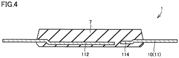
- Fig. 4 is a sectional view taken along a line IV-IV of Fig. 2 .
- Fig. 4 illustrates a section of a central portion of a lead frame.
- Semiconductor device 1 includes a base member 10, a semiconductor element 20, solder 30, wires 40, 41, and a sealing resin 7.
- semiconductor device 1 is a power module for power.
- base member 10 is a lead frame 11.
- a material for lead frame 11 is copper.
- dimensions of lead frame 11 are 120 mm in length, 75 mm in width, and 0.6 mm in thickness.
- Lead frame 11 includes a die pad 112, a main electrode terminal 113, and a signal terminal 114 such as a gate electrode terminal.
- semiconductor element 20 is mounted on base member 10.
- semiconductor element 20 is a power semiconductor element for power.
- semiconductor element 20 includes a diode 21 and an insulated gate bipolar transistor (IGBT) 22.
- IGBT 22 insulated gate bipolar transistor
- dimensions of diode 21 are 15 mm in length, 13 mm in width, and 0.2 mm in thickness.
- IGBT 22 are 15 mm in length, 15 mm in width, and 0.2 mm in thickness.
- Diode 21 and IGBT 22 are die-bonded to die pad 112 of lead frame 11 with solder 30.
- MOSFET metal oxide semiconductor field effect transistor
- Semiconductor element 20 may be a power semiconductor element using silicon (Si).
- semiconductor element 20 may be a wide band gap compound semiconductor using silicon carbide (SiC), gallium nitride (GaN), gallium arsenide (GaAs), or the like.
- solder 30 On die pad 112 of lead frame 11, two diodes 21 and two IGBTs 22 are die-bonded by solder 30.
- a composition ratio of solder 30 is 96.5 mass% of tin (Sn), 3 mass% of silver (Ag), and 0.5 mass% of copper (Cu).
- a melting point of solder 30 is 217 °C.
- the composition ratio of solder 30 may be 98.5 mass% of tin (Sn), 1 mass% of silver (Ag), and 0.5 mass% of copper (Cu).
- the composition ratio of solder 30 may be 96 mass% of tin (Sn), 3 mass% of antimony (Sb), and 1 mass% of silver (Ag).
- solder 30 a copper (Cu)-tin (Sn) paste in which a copper powder is dispersed to obtain high heat resistance by isothermal solidification, or a nano-silver paste joined using low temperature firing of nano-silver particles may be used instead of solder 30.
- a main electrode 211 of diode 21 and a main electrode 221 of IGBT 22 are electrically connected to lead frame 11 using wire 40.
- the material of wire 40 is aluminum.
- the diameter of wire 40 is 0.3 mm.
- a signal electrode 222 such as a gate electrode of IGBT 22 is electrically connected to lead frame 11 using wire 41.
- the material of wire 41 is aluminum.
- the diameter of wire 41 is 0.15 mm.
- wires 40, 41 may be copper (Cu), gold (Au), or Ag (silver).
- wires 40, 41 may be aluminum (Al)-coated copper (Cu) wires.
- ribbon bonding may be used, or the semiconductor element may be directly soldered to a plate-shaped electrode plate.
- Sealing resin 7 seals base member 10, semiconductor element 20, solder 30, and wires 40, 41. Heated sealing resin 7 is pressure-injected and then heat-cured while lead frame 11, semiconductor element 20, solder 30, and wires 40, 41 are sandwiched between molds (not illustrated), whereby resin sealing is completed.
- the mold (not illustrated) is heated to 170 °C.
- sealing resin 7 is heated to 170 °C.
- sealing resin 7 is an epoxy transfer mold resin containing a silica filler.
- sealing resin 7 is, pressure-injected and then heat-cured in an oven at 170 °C for 4 hours.
- FIGs. 5 and 6 are sectional views at sectional positions corresponding to Fig. 4 .
- test piece 72 for the adhesion evaluation test is formed on base member 10 from sealing resin 7 of semiconductor device 1.
- test piece 72 is formed from sealing resin 7 by processing using a laser beam 6.
- Laser beam 6 is a laser for opening the sealing resin.
- sealing resin 7 is removed in a circular shape using laser beam 6 to form a recess 71.
- an outermost surface diameter of recess 71 is 5.0 mm.
- an irradiation device of laser beam 6 is F/Alit manufactured by Shinohara Japan Co., Ltd.
- a wavelength of laser beam 6 is 1064 nm.
- maximum output of the laser beam 6 is 20 W.
- sealing resin 7 is further removed, and an outer peripheral portion is removed while the central portion of test piece 72 is left at a point of time when the remaining height of sealing resin 7 becomes, for example, 1.5 mm.
- the diameter of the central portion of test piece 72 is 1.5 mm. In this way, test piece 72 is manufactured.
- test piece 72 is formed in a pudding cup shape. That is, test piece 72 is formed in a truncated cone shape.
- a diameter D1 of the lead frame interface of test piece 72 is 1.94 mm.
- a diameter D2 of the surface of test piece 72 is 1.5 mm.
- a height H of test piece 72 is 1.5 mm.
- FIG. 8 is a top view illustrating semiconductor device 1 in which test piece 72 is formed in the method for manufacturing the test piece for the adhesion evaluation test of the first embodiment.
- a part of sealing resin 7 is indicated by a broken line
- lead frame 11 inside sealing resin 7 is indicated by a solid line
- semiconductor element 20 and the like are not illustrated.
- the adhesion evaluation method of the first embodiment is evaluated using the test piece manufactured by the method for manufacturing the test piece for the adhesion evaluation test.
- the adhesion evaluation method of the first embodiment includes process S100 of preparing semiconductor device 1, process S200 of forming test piece 72 for the adhesion evaluation test, and a process S300 of measuring the shear peeling strength.
- process S100 of preparing semiconductor device 1 and process S200 of forming test piece 72 for the adhesion evaluation test are the same as the method of manufacturing the test piece for the adhesion evaluation test described above, the description thereof will not be repeated.
- the shear peeling strength of the first embodiment is measured using test piece 72 for the adhesion evaluation test.
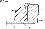
- Semiconductor device 1 in which test piece 72 is provided is fixed to a mounting table 80. In this state, test piece 72 is pushed by tool 90 until test piece 72 is broken.
- a device used for evaluating the shear peeling strength is bond tester DAGE4000 manufactured by DAGE.
- the shear peeling strength test is performed at normal temperature.
- the height of the tip end of tool 90 is set to the height of 0.04 mm from lead frame 11.
- the shear rate pressing tool 90 is 0.3 mm/s.
- An adhesive area of each sample is calculated after break of test piece 72, and a value obtained by dividing a breaking load by the adhesive area is defined as the shear peeling strength (Kg/mm).
- the shear peeling strength test is not limited to room temperature.
- the shear peeling strength test is performed at a high temperature such as 50 °C or 100 °C as necessary, whereby the adhesion in an actual use environment can be evaluated.
- test piece 72 for the adhesion evaluation test is formed on base member 10 from sealing resin 7 of semiconductor device 1.
- test piece 72 for the adhesion evaluation test can be formed on base member 10 from sealing resin 7 of semiconductor device 1 formed in the actual mass production mold. Consequently, it is possible to provide the method for manufacturing test piece 72 for the adhesion test in which the phenomenon generated in the actual mass production mold is directly reflected.
- test piece 72 is formed from sealing resin 7 by processing using laser beam 6. Consequently, test piece 72 can be formed from sealing resin 7 by processing using the laser beam. In addition, because test piece 72 is formed of sealing resin 7 by processing using the laser beam, dimensional accuracy of test piece 72 can be improved.
- test piece 72 for the adhesion evaluation test is formed on base member 10 from sealing resin 7 of semiconductor device 1.
- the shear peeling strength is measured using test piece 72 for the adhesion evaluation test. Consequently, the adhesion evaluation method in which the phenomenon generated in the actual mass production mold is directly reflected can be provided.
- test piece 72 may be manufactured on not only die pad 112 but also signal terminal 114. According to the first embodiment, test piece 72 can be manufactured at an arbitrary position on the lead frame 11, and the adhesion can be evaluated at a pinpoint of a place where the peeling between sealing resin 7 and lead frame 11 is easily generated in tests of long-term reliability and reflow heat resistance.
- Lead frame 11 may be plated with silver (Ag), gold (Au), nickel (Ni), tin (Sn), or the like. Generally, it is known that the adhesion to sealing resin 7 on these plating members is lower than that of copper (Cu). According to the first embodiment, in combination with a plating member, the adhesion can be evaluated at the pinpoint of the place where the peeling between sealing resin 7 and lead frame 11 is easily generated in the tests of the long-term reliability and reflow heat resistance.
- the adhesion at the position where the product is easily peeled off or the adhesion at the position where the adhesion of the product is low can be evaluated.
- the process condition during transfer molding is changed to use the first embodiment, so that the difference in adhesion due to the process condition that cannot be conventionally evaluated can be evaluated.
- an appropriate process condition can be determined before reliability is input, so that a development period can be shortened.
- Figs. 11 and 12 are sectional views at sectional positions corresponding to Fig. 5 .
- the outer peripheral portion of test piece 72 is removed from the beginning.
- sealing resin 7 is further removed to manufacture test piece 72.
- test piece 72 may be manufactured by removing only the outer peripheral portion of test piece 72 from the beginning.
- FIG. 13 is a top view illustrating semiconductor device 1 in the second modification of the method for manufacturing the test piece for the adhesion evaluation test of the first embodiment.
- a part of sealing resin 7 is indicated by the broken line
- lead frame 11 inside sealing resin 7 is indicated by the solid line
- semiconductor element 20 and the like are not illustrated.
- test piece 72 is formed in an elliptical truncated cone shape.
- the bottom surface and the top surface of test piece 72 may be formed in an oval or rounded rectangular shape.
- sealing resin 7 hardly remains or die pad 112 is exposed from sealing resin 7.
- the dimension (major axis) in a longitudinal direction is 1.5 times the dimension (minor axis) in a lateral direction.
- test piece 72 is formed in an elliptical truncated cone shape.
- the shear peeling strength is measured in the longitudinal direction of test piece 72, so that the evaluation in which an increase in strength due to deflection is removed can be performed when the adhesion of the minute region is evaluated.
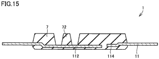
- Figs. 14 to 15 are sectional views at sectional positions corresponding to Fig. 5 .
- test piece 72 is formed from sealing resin 7 by processing using etching solution 110.
- a mask 100 is formed on sealing resin 7.
- Mask 100 is formed so as not to cover the periphery of test piece 72.
- Etching solution 110 dissolves sealing resin 7.
- Sealing resin 7 is etched into a truncated cone shape by etching solution 110.
- etching solution 110 As illustrated in Fig. 15 , after sealing resin 7 is etched into a truncated cone shape by etching solution 110, mask 100 is removed. Thus, the truncated cone-shaped test piece 72 is formed.
- test piece 72 is formed from sealing resin 7 by processing using an etching solution.
- test piece 72 can be manufactured in a larger amount at one time than the case where test piece 72 is formed of sealing resin 7 by processing using a laser.
- a second embodiment has the same configuration, operation, and effect as those of the first embodiment described above unless otherwise specified. Consequently, in the second embodiment, the same component as that in the first embodiment is denoted by the same reference numeral, and the description thereof will not be repeated.
- An adhesion evaluation method of the second embodiment is the same as the adhesion evaluation method of the first embodiment unless otherwise specified.
- FIG. 16 is a sectional view illustrating semiconductor device 1 in the method for manufacturing the test piece for the adhesion evaluation test of the second embodiment.
- Semiconductor device 1 includes base member 10, a base plate 14, semiconductor element 20, solder 30, wires 40, 41, sealing resin 7, a case 60, a signal terminal 61, and a main electrode terminal 62.
- base member 10 is a ceramic substrate 15.
- Ceramic substrate 15 includes a main body 15a and conductor layers 15b, 15c. Conductor layers 15b, 15c are attached to both surfaces of main body 15a, respectively.
- the material of main body 15a is aluminum nitride ceramic.
- the outer dimensions of main body 15a are 35 mm in length, 65 mm in width, and 0.64 mm in thickness.
- the material of conductor layers 15b, 15c is copper.
- the outer dimensions of conductor layers 15b, 15c are 31 mm in length, 61 mm in width, and 0.4 mm in thickness.
- Ceramic substrate 15 is bonded onto base plate 14 with solder 30. Specifically, conductor layer 15b of ceramic substrate 15 is bonded to base plate 14 with solder 30.
- the material of base plate 14 is copper.
- semiconductor element 20 includes diode 21 and IGBT 22.
- the dimensions of the diode 21 are 13 mm in length, 10 mm in width, and 0.2 mm in thickness.
- the dimensions of IGBT 22 are 13 mm in length, 13 mm in width, and 0.2 mm in thickness.
- Diode 21 and IGBT 22 are bonded onto conductor layer 15c of ceramic substrate 15 with solder 30.
- Semiconductor element 20 may be a power semiconductor element using silicon (Si).
- semiconductor element 20 may be a wide band gap compound semiconductor using silicon carbide (SiC), gallium nitride (GaN), gallium arsenide (GaAs), or the like.
- a composition ratio of solder 30 is 96 mass% of tin (Sn), 3.5 mass% of silver (Ag), and 0.5 mass% of copper (Cu).
- the composition ratio of solder 30 may be 98.5 mass% of tin (Sn), 1 mass% of silver (Ag), and 0.5 mass% of copper (Cu).
- the composition ratio of solder 30 may be 96 mass% of tin (Sn), 3 mass% of antimony (Sb), and 1 mass% of silver (Ag).
- solder 30 a copper (Cu)-tin (Sn) paste in which a copper powder is dispersed to obtain high heat resistance by isothermal solidification, or a nano-silver paste joined using low temperature firing of nano-silver particles may be used instead of solder 30.
- Main electrode 211 of diode 21 and main electrode of IGBT 22 are electrically connected to main electrode terminal 62 using wire 40.
- the material of wire 40 is aluminum.
- the diameter of the wire is 0.3 mm.
- the signal electrode such as the gate electrode of IGBT 22 is electrically connected to signal terminal 61 using wire 41.
- the material of wire 41 is aluminum.
- the diameter of the wire is 0.15 mm.
- wires 40, 41 may be copper (Cu) or gold (Au).
- wires 40, 41 may be aluminum (Al)-coated copper (Cu) wires.
- ribbon bonding may be used, or the semiconductor element may be directly soldered to a plate-shaped electrode plate.
- Signal terminal 61 and main electrode terminal 62 are insert-formed in case 60.
- the outer dimensions of case 60 are 75 mm in length, 75 mm in width, and 8 mm in thickness.
- Base plate 14 ceramic substrate 15, diode 21, IGBT 22, solder 30, wires 40, 41, sealing resin 7, signal terminal 61, and main electrode terminal 62 are disposed inside case 60.
- sealing resin 7 is formed by heating and curing a liquid sealing agent filled in case 60.
- the liquid seal agent includes an epoxy resin in which a silica filler is dispersed, a softening agent, an antifoaming agent, and a flame retardant.
- the liquid seal agent is cured by being heated at 100 °C for 1.5 hours and further heated at 140 °C for 1.5 hours using, for example, the oven.
- Fig. 17 illustrates a section of a portion of semiconductor device 1 where semiconductor element 20 does not exist.
- Test piece 72 is formed from sealing resin 7 by processing using laser beam 6.
- Laser beam 6 is a laser for opening the sealing resin.
- sealing resin 7 is removed in a circular shape using laser beam 6 to form a recess 71.
- an outermost surface diameter of recess 71 is 5.0 mm.
- an irradiation device of laser beam 6 is F/Alit manufactured by Shinohara Japan Co., Ltd.
- a wavelength of laser beam 6 is 1064 nm.
- maximum output of the laser beam 6 is 20 W.
- Sealing resin 7 is further removed, and an outer peripheral portion is removed while the central portion of test piece 72 is left at a point of time when the remaining height of sealing resin 7 becomes, for example, 1.5 mm.
- the diameter of the central portion of test piece 72 is 1.5 mm. In this way, test piece 72 is manufactured.
- Test piece 72 is formed in a pudding cup shape. That is, test piece 72 is formed in a truncated cone shape.
- the diameter of the lead frame interface of test piece 72 is 1.94 mm.
- the diameter of the surface of test piece 72 is 1.5 mm.
- the height of test piece 72 is 1.5 mm.
- the method for manufacturing test piece 72 for the adhesion evaluation test of the second embodiment the method for manufacturing test piece 72 for the adhesion test in which the phenomenon generated in the actual mass production mold is directly reflected can be provided similarly to the first embodiment.
- test piece 72 for the adhesion evaluation test is formed on base member 10 from sealing resin 7 of semiconductor device 1.
- the shear peeling strength is measured using test piece 72 for the adhesion evaluation test. Consequently, the adhesion evaluation method in which the phenomenon generated in the actual mass production mold is directly reflected can be provided similarly to the first embodiment.
- semiconductor device 1 is prepared.
- semiconductor device 1 includes lead frame 11, diode 21, IGBT 22, solder 30, wires 40, 41, and sealing resin 7.
- lead frame 11 The material of lead frame 11 is copper.
- the dimensions of lead frame 11 are 120 mm in length, 75 mm in width, and 0.6 mm in thickness.
- diode 21 The dimensions of diode 21 are 15 mm in length, 13 mm in width, and 0.2 mm in thickness.
- IGBT 22 are 15 mm in length, 15 mm in width, and 0.2 mm in thickness.
- Diode 21 and IGBT 22 are die-bonded to die pad 112 of lead frame 11 with solder 30.
- the composition ratio of solder 30 is 96.5 mass% of tin (Sn), 3 mass% of silver (Ag), and 0.5 mass% of copper (Cu).
- the melting point of solder 30 is 217 °C.
- a main electrode 211 of diode 21 and a main electrode 221 of IGBT 22 are electrically connected to lead frame 11 using wire 40.
- the material of wire 40 is aluminum.
- the diameter of wire 40 is 0.3 mm.
- a signal electrode 222 such as a gate electrode of IGBT 22 is electrically connected to lead frame 11 using wire 41.
- the material of wire 41 is aluminum.
- the diameter of wire 41 is 0.15 mm.
- Heated sealing resin 7 is pressure-injected and then heat-cured while lead frame 11, semiconductor element 20, solder 30, and wires 40, 41 are sandwiched between molds (not illustrated), whereby resin sealing is completed.
- the mold (not illustrated) is heated to 170 °C.
- Sealing resin 7 is heated to 170 °C.
- Sealing resin 7 is an epoxy transfer mold resin containing a silica filler. Sealing resin 7 is pressure-injected and then heat-cured in the oven at 170 °C for 4 hours.
- test piece 72 for the adhesion evaluation test is formed.
- Recess 71 is formed by removing sealing resin 7 in a circular shape using laser beam 6.
- the outermost surface diameter of recess 71 is 5.0 mm.
- the irradiation device of laser beam 6 is F/Alit manufactured by Shinohara Japan Co., Ltd.
- the wavelength of laser beam 6 is 1064 nm.
- the maximum output of laser beam 6 is 20 W.
- Sealing resin 7 is further removed, and an outer peripheral portion is removed while the central portion of test piece 72 is left at a point of time when the remaining height of sealing resin 7 becomes 1.5 mm.
- the diameter of the central portion of test piece 72 is 1.5 mm.
- Test piece 72 is formed in a pudding cup shape. That is, test piece 72 is formed in a truncated cone shape. Diameter D1 of the lead frame interface of test piece 72 is 1.94 mm. Diameter D2 of the surface of test piece 72 is 1.5 mm. Height H of test piece 72 is 1.5 mm.
- the adhesion evaluation method of the example is evaluated using the test piece manufactured by the method for manufacturing the test piece for the adhesion evaluation test.
- the shear peeling strength is measured using the test piece for the adhesion evaluation test.
- test piece 72 is fixed to a mounting table 80. In this state, test piece 72 is pushed by tool 90 until test piece 72 is broken.
- the device used for evaluating the shear peeling strength is bond tester DAGE4000 manufactured by DAGE.
- the shear peeling strength test is performed at normal temperature.
- the height of the tip end of tool 90 is set to the height of 0.04 mm from lead frame 11.
- the shear rate pressing tool 90 is 0.3 mm/s.
- Fig. 18 is a graph illustrating the relationship between the laser irradiation condition (a resin remaining amount around the test piece) and the shear peeling strength.
- the shear peeling strength of test piece 72 was examined by changing the laser irradiation time.
- the height of test piece 72 is 1.5 mm.
- the diameter of the interface of lead frame 11 of test piece 72 is 1.94 mm.
- the laser irradiation conditions are the following conditions (a), (b), (c).
- condition (a) the sealing resin remaining thickness around the test piece is greater than or equal to 0 mm and less than or equal to 0.07 mm.
- condition (b) the copper lead frame is exposed from the sealing resin around the test piece.
- condition (c) the periphery of the test piece is irradiated with the excessive laser beam.
- the standard deviation ⁇ 0.16
- the periphery of the test piece is irradiated with the laser beam twice after the copper lead frame is exposed at the intensity of the laser beam capable of removing the sealing resin having the thickness of about 0.5 mm by one-time irradiation.
- Fig. 19 illustrates the appearance of prepared test piece 72 and the appearance of the adhesive portion after the shear peeling test.
- condition (c) a burnt mark of the copper lead frame was observed around test piece 72.
- the copper lead frame was not cut into a concave shape, and the overall shape was not different from the condition (b).
- Fig. 21 is a graph illustrating the relationship between the diameter of the test piece and the shear peeling strength.
- Five specifications of test pieces were prepared. In each of the five specifications, diameter D1 of the interface of lead frame 11 of test piece 72 is 1.94 mm, 1.74 mm, 1.43 mm, 1.24 mm, 0.9 mm. Seven test pieces of five specifications were prepared. Each test piece was subjected to the shear peeling test. The average value of the shear peeling strength was calculated for each of the five specifications. As a result, the shear peeling strength was larger as diameter D1 of the interface of lead frame 11 of test piece 72 was smaller. That is, the shear peeling strength tended to increase as the adhesion area was smaller.
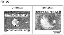
- Fig. 22 illustrates the appearance after the shear peeling test when diameter D1 is 1.94 mm and 0.90 mm.
- the mode was almost interfacial peeling when diameter D1 was 1.94 mm, whereas the mode was cohesive peeling when diameter D1 was 0.90 mm.
- the pudding cup of the test piece is thin, the deflection is generated against the load applied from the tool to apply the stress to the inside of the pudding cup separately from the interface.
- the interfacial peeling the peeling is generated at the interface, and the copper lead frame is completely exposed.
- the cohesive peeling the destruction is generated in a bulk portion of the resin.
- Fig. 23 is a sectional view illustrating the method of measuring the shear peeling strength of test piece 72. It is considered that when the diameter of test piece 72 decreases, the deflection of test piece 72 is easily generated up to the height that tool 90 hits test piece 72 and the shear peeling strength is measured to be large. It has been found that the shear peeling strength tends to increase as the height actually hit by tool 90 is increased.
- Figs. 24 and 25 the relationship between the direction pressed by the tool and the shear peeling strength was compared when the upper surface and the bottom surface of test piece 72 had a round corner rectangular shape.
- Fig. 24 compares the relationship between the direction in which the test piece is pushed by the tool and the shear peeling strength.
- Fig. 25 illustrates the shape of test piece 72 and the direction in which the test piece is pushed by the tool. The shear peeling strength was larger when test piece 72 was pushed in the lateral direction than when the test piece was pushed in the longitudinal direction.
- test piece 72 is formed in the elliptical truncated cone shape, specifically, the upper surface and the bottom surface are formed in the rounded rectangular shape, the influence of the deflection can be excluded by pushing test piece 72 with the tool from the longitudinal direction even when the bottom area of test piece 72 is small.
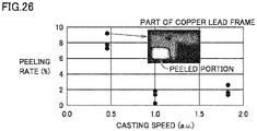
- Fig. 26 illustrates the relationship between the casting speed and the peeling rate when a package in which the resin casting speed is changed is prepared and when a reflow heat resistance test is performed.
- Fig. 26 illustrates a scanning acoustic tomograph (SAT) image of a part of the copper lead frame.
- the peeling rate is defined as a ratio of the peeling area to the entire area of the copper lead frame.
- the casting speed indicates a numerical value when the median value is 1.0. A clear correlation between the casting speed and the peeling rate cannot be obtained, but there is a possibility that the physical property of the material such as a gelation time of the resin is affected.
- the shear peeling strength before the reflow heat resistance test of the package in which the casting speed of the resin was changed was evaluated.
- the pudding cup was prepared at a position where a peeling generation rate was high in the reflow heat resistance test. Diameter D1 of the pudding cup was set to 0.9 mm due to the restriction of the area of the copper lead frame.
- Fig. 27 illustrates the relationship between the casting speed of the resin and the shear peeling strength. It was found that the shear peeling strength was changed with respect to the resin casting speed.
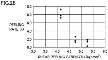
- Fig. 28 illustrates correlation between the shear peeling strength and the peeling rate in the reflow heat resistance test by combining the results in Figs. 26 and 27 . A negative correlation between the shear peeling strength and the peeling rate was found. The peeling rate in the reflow heat resistance test can be predicted by measuring the shear peeling strength using this technique.
- a third embodiment has the same configuration, operation, and effect as those of the first embodiment described above unless otherwise specified. Consequently, in the third embodiment, the same component as that in the first embodiment is denoted by the same reference numeral, and the description thereof will not be repeated.
- Fig. 29 is a sectional view illustrating semiconductor device 1 in the method for manufacturing the test piece for the adhesion evaluation test of the third embodiment.
- an insulating sheet 18 including insulating member 16 and metal member 17 is disposed under die pad 112.
- Insulating member 16 is an epoxy resin.
- Insulating member 16 is formed in a sheet shape. Insulating member 16 has an insulating property.
- the material of metal member 17 is copper or aluminum.
- Fig. 30 illustrates a section of a portion of semiconductor device 1 where semiconductor element 20 does not exist.
- test piece 72 is formed by laser beam 6 so as to include sealing resin 7 and insulating member 16 in a portion where die pad 112 is not disposed. In this way, test piece 72 for the adhesion evaluation test is formed on insulating member 16 under base member 10 from sealing resin 7 of semiconductor device 1.
- test piece 72 is pushed by tool 90.
- a height 120 of tool 90 is lower than a thickness 130 of insulating member 16.
- Height 120 of tool 90 is lower than thickness 130 of insulating member 16 by, for example, 0.1 mm.
- the adhesion between insulating member 16 and metal member 17 is required to be secured after insulating sheet 18 is sealed with the sealing resin 7.
- the checking of the presence or absence of the peeling by an ultrasonic test or the like after the reliability test is a general method, and the presence or absence of the degradation is hardly quantitatively checked as the evaluation of the adhesion.
- the influence of the injection process condition of sealing resin 7 on the adhesion strength of the interface between insulating member 16 and metal member 17 can be checked by the shear test method of the third embodiment.
- the appropriate process condition can be determined, so that the material development period of insulating member 16 can be shortened.
Landscapes
- Physics & Mathematics (AREA)
- Health & Medical Sciences (AREA)
- Life Sciences & Earth Sciences (AREA)
- Chemical & Material Sciences (AREA)
- Analytical Chemistry (AREA)
- Biochemistry (AREA)
- General Health & Medical Sciences (AREA)
- General Physics & Mathematics (AREA)
- Immunology (AREA)
- Pathology (AREA)
- Encapsulation Of And Coatings For Semiconductor Or Solid State Devices (AREA)
Abstract
Description
- The present disclosure relates to a method for manufacturing a test piece for an adhesion evaluation test and an adhesion evaluation method.
- Semiconductor devices such as power modules are used in products such as industrial equipment, household electrical equipment, and information terminals. Generally, in the semiconductor device, a semiconductor element, a lead frame, an insulating substrate, and the like are sealed by a sealing resin for the purpose of protecting and insulating the semiconductor element, the lead frame, the insulating substrate, and the like. The sealing resin is required to have long-term reliability, reflow heat resistance, high reliability for a temperature cycle, and the like. For this reason, adhesion of the sealing resin to the lead frame, the insulating substrate, and the like are required to be quantitatively evaluated.
- Generally, a pudding cup test is used as a method for evaluating the adhesion of the sealing resin. In the pudding cup test, a truncated cone-shaped test piece made of the same resin as the sealing resin is formed on the surface of a base member. A load is applied to the test piece along the surface of the base member, and the load during destruction of a bonding portion of the sealing resin is measured.
- PTL 1 (
Japanese Patent Laying-Open No. 2014-146704 - The pudding cup test is also described in a semiconductor equipment and materials international (SEMI) standard G69-0996.
- PTL 1:
Japanese Patent Laying-Open No. 2014-146704 - In the pudding cup test described in
PTL 1, because a dedicated mold preparing the test piece for the pudding cup test is used, it is difficult to reproduce process conditions such as an injection condition in an actual mass production mold. Consequently, it is difficult to produce a test piece for an adhesion test in which a phenomenon generated in the actual mass production mold is directly reflected. - The SEMI standard G69-0996 does not describe a method for manufacturing the test piece for the pudding cup test.
- The present disclosure has been made in view of the above problems, and an object of the present disclosure is to provide a method for manufacturing the test piece for the adhesion test in which the phenomenon generated in the actual mass production mold is directly reflected, and an adhesion evaluation method.
- A method for manufacturing a test piece for an adhesion evaluation test of the present disclosure includes preparing a semiconductor device and forming a test piece for the adhesion evaluation test. In preparing the semiconductor device, the semiconductor device includes a base member, a semiconductor element mounted on the base member, and a sealing resin to seal the base member and the semiconductor element. In forming the test piece for the adhesion evaluation test, the test piece for the adhesion evaluation test is formed on the base member from the sealing resin of the semiconductor device.
- According to the method for manufacturing the test piece for the adhesion evaluation test of the present disclosure, the test piece for the adhesion evaluation test is formed on the base member from the sealing resin of the semiconductor device. Thus, the test piece for the adhesion evaluation test can be formed on the base member from the sealing resin of the semiconductor device formed in the actual mass production mold. Consequently, it is possible to provide the method for manufacturing the test piece for the adhesion test and the adhesion evaluation method in which the phenomenon generated in the actual mass production mold is directly reflected.
-
-
Fig. 1 is a flowchart illustrating a method for manufacturing a test piece for an adhesion evaluation test according to a first embodiment. -
Fig. 2 is a perspective view illustrating a process of preparing a semiconductor device in the method for manufacturing the test piece for the adhesion evaluation test of the first embodiment. -
Fig. 3 is a sectional view taken along a line III-III inFig. 2 . -
Fig. 4 is a sectional view taken along a line IV-IV ofFig. 2 . -
Fig. 5 is a sectional view illustrating a process of forming the test piece for the adhesion evaluation test in the method for manufacturing the test piece for the adhesion evaluation test of the first embodiment. -
Fig. 6 is a sectional view illustrating a state in which a sealing resin is further removed fromFig. 5 to form the test piece. -
Fig. 7 is a perspective view illustrating the test piece for the adhesion evaluation test of the first embodiment. -
Fig. 8 is a plan view illustrating a semiconductor device on which the test piece for the adhesion evaluation test of the first embodiment is formed. -
Fig. 9 is a flowchart illustrating an adhesion evaluation method of the first embodiment. -
Fig. 10 is a sectional view illustrating a process of measuring shear peeling strength in the adhesion evaluation method of the first embodiment. -
Fig. 11 is a sectional view illustrating a first modification of the method for manufacturing the test piece for the adhesion evaluation test of the first embodiment. -
Fig. 12 is a sectional view illustrating a state in which the sealing resin is further removed fromFig. 11 to form the test piece. -
Fig. 13 is a plan view illustrating a second modification of the method for manufacturing the test piece for the adhesion evaluation test of the first embodiment. -
Fig. 14 is a sectional view illustrating a third modification of the method for manufacturing the test piece for the adhesion evaluation test of the first embodiment. -
Fig. 15 is a sectional view illustrating a state in which a mask is removed fromFig. 14 to form the test piece. -
Fig. 16 is a sectional view illustrating a process of preparing a semiconductor device in a method for manufacturing a test piece for an adhesion evaluation test according to a second embodiment. -
Fig. 17 is a sectional view illustrating a process of forming the test piece for the adhesion evaluation test in the method for manufacturing the test piece for the adhesion evaluation test of the second embodiment. -
Fig. 18 is a graph illustrating a relationship between a laser irradiation time and the shear peeling strength in an example. -
Fig. 19 is a photograph illustrating an appearance of the test piece and an appearance of an adhesive portion after a shear test. -
Fig. 20 is a sectional view illustrating a state in which unevenness of the sealing resin exists around the test piece of the example. -
Fig. 21 is a graph illustrating the relationship between a diameter of the test piece and the shear peeling strength in the example. -
Fig. 22 is a photograph illustrating an appearance after a shear peeling test when the diameters of the test pieces are 1.94 mm and 0.9 mm. -
Fig. 23 is a sectional view illustrating a method for measuring the shear peeling strength of the test piece in the example. -
Fig. 24 is a graph illustrating the relationship between a direction in which the test piece is pushed by a tool and the shear peeling strength. -
Fig. 25 is a perspective view illustrating a shape of the test piece and the direction in which the test piece is pushed by the tool. -
Fig. 26 is a graph illustrating a relationship between a casting speed and a peeling rate. -
Fig. 27 is a graph illustrating a relationship between the casting speed and the shear peeling strength. -
Fig. 28 is a graph illustrating a relationship between the peeling rate and the shear peeling strength. -
Fig. 29 is a sectional view illustrating a process of preparing a semiconductor device in a method for manufacturing a test piece for an adhesion evaluation test according to a third embodiment. -
Fig. 30 is a sectional view illustrating a process of forming the test piece for the adhesion evaluation test in the method for manufacturing the test piece for the adhesion evaluation test of the third embodiment. -
Fig. 31 is a sectional view illustrating a process of measuring shear peeling strength in the adhesion evaluation method of the third embodiment. - Hereinafter, embodiments will be described with reference to the drawings. In the following description, the same or corresponding parts are denoted by the same reference numerals, and overlapping description will not be repeated.
- With reference to
Figs. 1 to 10 , a method for manufacturing a test piece for an adhesion evaluation test and an adhesion evaluation method according to a first embodiment will be described. - With reference to
Figs. 1 to 7 , the method for manufacturing the test piece for the adhesion evaluation test of the first embodiment will be described below. With reference toFig. 1 , the method for manufacturing the test piece for the adhesion evaluation test of the first embodiment includes a process S100 of preparing asemiconductor device 1 and a process S200 of forming atest piece 72 for the adhesion evaluation test. - With reference to
Figs. 2 to 4 , a process of preparing a semiconductor device in the method for manufacturing the test piece for the adhesion evaluation test of the first embodiment will be described.Fig. 2 is a perspective view illustratingsemiconductor device 1 in the method for manufacturing the test piece for the adhesion evaluation test of the first embodiment. InFig. 2 , a sealing resin is not illustrated for easy viewing of an internal structure.Fig. 3 is a sectional view taken along a line III-III ofFig. 2 .Fig. 4 is a sectional view taken along a line IV-IV ofFig. 2 .Fig. 4 illustrates a section of a central portion of a lead frame. -
Semiconductor device 1 includes abase member 10, asemiconductor element 20,solder 30,wires resin 7. For example,semiconductor device 1 is a power module for power. - In the first embodiment,
base member 10 is alead frame 11. For example, a material forlead frame 11 is copper. For example, dimensions oflead frame 11 are 120 mm in length, 75 mm in width, and 0.6 mm in thickness.Lead frame 11 includes adie pad 112, amain electrode terminal 113, and asignal terminal 114 such as a gate electrode terminal. -
Semiconductor element 20 is mounted onbase member 10. For example,semiconductor element 20 is a power semiconductor element for power. In the first embodiment,semiconductor element 20 includes adiode 21 and an insulated gate bipolar transistor (IGBT) 22. For example, dimensions ofdiode 21 are 15 mm in length, 13 mm in width, and 0.2 mm in thickness. For example, dimensions ofIGBT 22 are 15 mm in length, 15 mm in width, and 0.2 mm in thickness.Diode 21 andIGBT 22 are die-bonded to diepad 112 oflead frame 11 withsolder 30. - A metal oxide semiconductor field effect transistor (MOSFET) or the like can be used as
semiconductor element 20. -
Semiconductor element 20 may be a power semiconductor element using silicon (Si). In addition,semiconductor element 20 may be a wide band gap compound semiconductor using silicon carbide (SiC), gallium nitride (GaN), gallium arsenide (GaAs), or the like. - On
die pad 112 oflead frame 11, twodiodes 21 and twoIGBTs 22 are die-bonded bysolder 30. For example, a composition ratio ofsolder 30 is 96.5 mass% of tin (Sn), 3 mass% of silver (Ag), and 0.5 mass% of copper (Cu). For example, a melting point ofsolder 30 is 217 °C. - For example, the composition ratio of
solder 30 may be 98.5 mass% of tin (Sn), 1 mass% of silver (Ag), and 0.5 mass% of copper (Cu). For example, the composition ratio ofsolder 30 may be 96 mass% of tin (Sn), 3 mass% of antimony (Sb), and 1 mass% of silver (Ag). - In addition, a copper (Cu)-tin (Sn) paste in which a copper powder is dispersed to obtain high heat resistance by isothermal solidification, or a nano-silver paste joined using low temperature firing of nano-silver particles may be used instead of
solder 30. - A
main electrode 211 ofdiode 21 and amain electrode 221 ofIGBT 22 are electrically connected to leadframe 11 usingwire 40. For example, the material ofwire 40 is aluminum. For example, the diameter ofwire 40 is 0.3 mm. - A
signal electrode 222 such as a gate electrode ofIGBT 22 is electrically connected to leadframe 11 usingwire 41. For example, the material ofwire 41 is aluminum. For example, the diameter ofwire 41 is 0.15 mm. - For example, the material of
wires wires - Instead of using wire bonding for circuit formation, ribbon bonding may be used, or the semiconductor element may be directly soldered to a plate-shaped electrode plate.
- Sealing
resin 7seals base member 10,semiconductor element 20,solder 30, andwires resin 7 is pressure-injected and then heat-cured whilelead frame 11,semiconductor element 20,solder 30, andwires resin 7 is heated to 170 °C. For example, sealingresin 7 is an epoxy transfer mold resin containing a silica filler. For example, sealingresin 7 is, pressure-injected and then heat-cured in an oven at 170 °C for 4 hours. - With reference to
Figs. 5 and6 , a process of forming the test piece for the adhesion evaluation test of the first embodiment will be described.Figs. 5 and6 are sectional views at sectional positions corresponding toFig. 4 . - As illustrated in
Figs. 5 and6 , in the process of forming the test piece for the adhesion evaluation test of the first embodiment,test piece 72 for the adhesion evaluation test is formed onbase member 10 from sealingresin 7 ofsemiconductor device 1. - As illustrated in
Fig. 5 ,test piece 72 is formed from sealingresin 7 by processing using alaser beam 6.Laser beam 6 is a laser for opening the sealing resin. First, sealingresin 7 is removed in a circular shape usinglaser beam 6 to form arecess 71. For example, an outermost surface diameter ofrecess 71 is 5.0 mm. - For example, an irradiation device of
laser beam 6 is F/Alit manufactured by Shinohara Japan Co., Ltd. For example, a wavelength oflaser beam 6 is 1064 nm. For example, maximum output of thelaser beam 6 is 20 W. - As illustrated in
Fig. 6 , sealingresin 7 is further removed, and an outer peripheral portion is removed while the central portion oftest piece 72 is left at a point of time when the remaining height of sealingresin 7 becomes, for example, 1.5 mm. For example, the diameter of the central portion oftest piece 72 is 1.5 mm. In this way,test piece 72 is manufactured. - With reference to
Figs. 6 and7 ,test piece 72 is formed in a pudding cup shape. That is,test piece 72 is formed in a truncated cone shape. For example, a diameter D1 of the lead frame interface oftest piece 72 is 1.94 mm. For example, a diameter D2 of the surface oftest piece 72 is 1.5 mm. For example, a height H oftest piece 72 is 1.5 mm. - With reference to
Fig. 8 ,semiconductor device 1 on whichtest piece 72 is formed will be described. Sealingresin 7 hardly remains around truncated cone-shapedtest piece 72. Alternatively, diepad 112 is exposed from sealingresin 7 around truncated cone-shapedtest piece 72.Fig. 8 is a top view illustratingsemiconductor device 1 in whichtest piece 72 is formed in the method for manufacturing the test piece for the adhesion evaluation test of the first embodiment. InFig. 8 , for easy viewing, a part of sealingresin 7 is indicated by a broken line,lead frame 11 inside sealingresin 7 is indicated by a solid line, andsemiconductor element 20 and the like are not illustrated. - An adhesion evaluation method of the first embodiment will be described below.
- In the adhesion evaluation method of the first embodiment, the adhesion is evaluated using the test piece manufactured by the method for manufacturing the test piece for the adhesion evaluation test.
- With reference to
Fig. 9 , the adhesion evaluation method of the first embodiment includes process S100 of preparingsemiconductor device 1, process S200 of formingtest piece 72 for the adhesion evaluation test, and a process S300 of measuring the shear peeling strength. - Because process S100 of preparing
semiconductor device 1 and process S200 of formingtest piece 72 for the adhesion evaluation test are the same as the method of manufacturing the test piece for the adhesion evaluation test described above, the description thereof will not be repeated. - With reference to
Fig. 10 , the process of measuring the shear peeling strength of the first embodiment will be described. In the process of measuring the shear peeling strength of the first embodiment, the shear peeling strength is measured usingtest piece 72 for the adhesion evaluation test.Semiconductor device 1 in whichtest piece 72 is provided is fixed to a mounting table 80. In this state,test piece 72 is pushed bytool 90 untiltest piece 72 is broken. - For example, a device used for evaluating the shear peeling strength is bond tester DAGE4000 manufactured by DAGE. For example, the shear peeling strength test is performed at normal temperature. For example, the height of the tip end of
tool 90 is set to the height of 0.04 mm fromlead frame 11. For example, the shearrate pressing tool 90 is 0.3 mm/s. An adhesive area of each sample is calculated after break oftest piece 72, and a value obtained by dividing a breaking load by the adhesive area is defined as the shear peeling strength (Kg/mm). - The shear peeling strength test is not limited to room temperature. The shear peeling strength test is performed at a high temperature such as 50 °C or 100 °C as necessary, whereby the adhesion in an actual use environment can be evaluated.
- An advantageous effect of the first embodiment will be described below.
- According to the method for
manufacturing test piece 72 for the adhesion evaluation test of the first embodiment,test piece 72 for the adhesion evaluation test is formed onbase member 10 from sealingresin 7 ofsemiconductor device 1. Thus,test piece 72 for the adhesion evaluation test can be formed onbase member 10 from sealingresin 7 ofsemiconductor device 1 formed in the actual mass production mold. Consequently, it is possible to provide the method formanufacturing test piece 72 for the adhesion test in which the phenomenon generated in the actual mass production mold is directly reflected. - In the method for
manufacturing test piece 72 for the adhesion evaluation test of the first embodiment,test piece 72 is formed from sealingresin 7 by processing usinglaser beam 6. Consequently,test piece 72 can be formed from sealingresin 7 by processing using the laser beam. In addition, becausetest piece 72 is formed of sealingresin 7 by processing using the laser beam, dimensional accuracy oftest piece 72 can be improved. - According to the adhesion evaluation method of the first embodiment,
test piece 72 for the adhesion evaluation test is formed onbase member 10 from sealingresin 7 ofsemiconductor device 1. The shear peeling strength is measured usingtest piece 72 for the adhesion evaluation test. Consequently, the adhesion evaluation method in which the phenomenon generated in the actual mass production mold is directly reflected can be provided. - In the first embodiment,
test piece 72 may be manufactured on not only diepad 112 but also signal terminal 114. According to the first embodiment,test piece 72 can be manufactured at an arbitrary position on thelead frame 11, and the adhesion can be evaluated at a pinpoint of a place where the peeling between sealingresin 7 and leadframe 11 is easily generated in tests of long-term reliability and reflow heat resistance. -
Lead frame 11 may be plated with silver (Ag), gold (Au), nickel (Ni), tin (Sn), or the like. Generally, it is known that the adhesion to sealingresin 7 on these plating members is lower than that of copper (Cu). According to the first embodiment, in combination with a plating member, the adhesion can be evaluated at the pinpoint of the place where the peeling between sealingresin 7 and leadframe 11 is easily generated in the tests of the long-term reliability and reflow heat resistance. - In the first embodiment, the adhesion at the position where the product is easily peeled off or the adhesion at the position where the adhesion of the product is low can be evaluated.
- Furthermore, the process condition during transfer molding is changed to use the first embodiment, so that the difference in adhesion due to the process condition that cannot be conventionally evaluated can be evaluated. Thus, an appropriate process condition can be determined before reliability is input, so that a development period can be shortened.
- Modification of the method for manufacturing the test piece for the adhesion evaluation test of the first embodiment will be described.
- With reference to
Figs. 11 to 12 , a first modification of the method for manufacturing the test piece for the adhesion evaluation test of the first embodiment will be described.Figs. 11 and12 are sectional views at sectional positions corresponding toFig. 5 . In the first modification of the method for manufacturing the test piece for the adhesion evaluation test of the first embodiment, as illustrated inFig. 11 , the outer peripheral portion oftest piece 72 is removed from the beginning. As illustrated inFig. 12 , sealingresin 7 is further removed to manufacturetest piece 72. In this way,test piece 72 may be manufactured by removing only the outer peripheral portion oftest piece 72 from the beginning. - With reference to
Fig. 13 , a second modification of the method for manufacturing the test piece for the adhesion evaluation test of the first embodiment will be described.Fig. 13 is a top view illustratingsemiconductor device 1 in the second modification of the method for manufacturing the test piece for the adhesion evaluation test of the first embodiment. InFig. 13 , for easy viewing, a part of sealingresin 7 is indicated by the broken line,lead frame 11 inside sealingresin 7 is indicated by the solid line, andsemiconductor element 20 and the like are not illustrated. - In the second modification of the method for manufacturing the test piece for the adhesion evaluation test of the first embodiment,
test piece 72 is formed in an elliptical truncated cone shape. The bottom surface and the top surface oftest piece 72 may be formed in an oval or rounded rectangular shape. Around elliptical truncated cone-shapedtest piece 72, sealingresin 7 hardly remains or diepad 112 is exposed from sealingresin 7. - In elliptical truncated cone-shaped
test piece 72, for example, the dimension (major axis) in a longitudinal direction is 1.5 times the dimension (minor axis) in a lateral direction. - In the second modification of the method for manufacturing the test piece for the adhesion evaluation test of the first embodiment,
test piece 72 is formed in an elliptical truncated cone shape. The shear peeling strength is measured in the longitudinal direction oftest piece 72, so that the evaluation in which an increase in strength due to deflection is removed can be performed when the adhesion of the minute region is evaluated. - With reference to
Figs. 14 to 15 , a third modification of the method for manufacturing the test piece for the adhesion evaluation test of the first embodiment will be described.Figs. 14 and15 are sectional views at sectional positions corresponding toFig. 5 . In the third modification of the method for manufacturing the test piece for the adhesion evaluation test of the first embodiment,test piece 72 is formed from sealingresin 7 by processing usingetching solution 110. - As illustrated in
Fig. 14 , first, amask 100 is formed on sealingresin 7.Mask 100 is formed so as not to cover the periphery oftest piece 72.Etching solution 110dissolves sealing resin 7. Sealingresin 7 is etched into a truncated cone shape by etchingsolution 110. - As illustrated in
Fig. 15 , after sealingresin 7 is etched into a truncated cone shape by etchingsolution 110,mask 100 is removed. Thus, the truncated cone-shapedtest piece 72 is formed. - According to the third modification of the method for manufacturing the test piece for the adhesion evaluation test of the first embodiment,
test piece 72 is formed from sealingresin 7 by processing using an etching solution. Thus,test piece 72 can be manufactured in a larger amount at one time than the case wheretest piece 72 is formed of sealingresin 7 by processing using a laser. - A second embodiment has the same configuration, operation, and effect as those of the first embodiment described above unless otherwise specified. Consequently, in the second embodiment, the same component as that in the first embodiment is denoted by the same reference numeral, and the description thereof will not be repeated.
- With reference to
Figs. 16 and17 , a method for manufacturing the test piece for the adhesion evaluation test of the second embodiment will be described. An adhesion evaluation method of the second embodiment is the same as the adhesion evaluation method of the first embodiment unless otherwise specified. - With reference to
Fig. 16 , a process of preparing the semiconductor device in the method for manufacturing the test piece for the adhesion evaluation test according to the second embodiment will be described.Fig. 16 is a sectional view illustratingsemiconductor device 1 in the method for manufacturing the test piece for the adhesion evaluation test of the second embodiment. -
Semiconductor device 1 includesbase member 10, abase plate 14,semiconductor element 20,solder 30,wires resin 7, acase 60, asignal terminal 61, and amain electrode terminal 62. - In the second embodiment,
base member 10 is aceramic substrate 15.Ceramic substrate 15 includes amain body 15a andconductor layers main body 15a, respectively. For example, the material ofmain body 15a is aluminum nitride ceramic. The outer dimensions ofmain body 15a are 35 mm in length, 65 mm in width, and 0.64 mm in thickness. For example, the material of conductor layers 15b, 15c is copper. The outer dimensions of conductor layers 15b, 15c are 31 mm in length, 61 mm in width, and 0.4 mm in thickness. -
Ceramic substrate 15 is bonded ontobase plate 14 withsolder 30. Specifically,conductor layer 15b ofceramic substrate 15 is bonded tobase plate 14 withsolder 30. For example, the material ofbase plate 14 is copper. - In the second embodiment,
semiconductor element 20 includesdiode 21 andIGBT 22. For example, the dimensions of thediode 21 are 13 mm in length, 10 mm in width, and 0.2 mm in thickness. For example, the dimensions ofIGBT 22 are 13 mm in length, 13 mm in width, and 0.2 mm in thickness.Diode 21 andIGBT 22 are bonded ontoconductor layer 15c ofceramic substrate 15 withsolder 30. -
Semiconductor element 20 may be a power semiconductor element using silicon (Si). In addition,semiconductor element 20 may be a wide band gap compound semiconductor using silicon carbide (SiC), gallium nitride (GaN), gallium arsenide (GaAs), or the like. - For example, a composition ratio of
solder 30 is 96 mass% of tin (Sn), 3.5 mass% of silver (Ag), and 0.5 mass% of copper (Cu). - For example, the composition ratio of
solder 30 may be 98.5 mass% of tin (Sn), 1 mass% of silver (Ag), and 0.5 mass% of copper (Cu). For example, the composition ratio ofsolder 30 may be 96 mass% of tin (Sn), 3 mass% of antimony (Sb), and 1 mass% of silver (Ag). - In addition, a copper (Cu)-tin (Sn) paste in which a copper powder is dispersed to obtain high heat resistance by isothermal solidification, or a nano-silver paste joined using low temperature firing of nano-silver particles may be used instead of
solder 30. -
Main electrode 211 ofdiode 21 and main electrode ofIGBT 22 are electrically connected tomain electrode terminal 62 usingwire 40. For example, the material ofwire 40 is aluminum. For example, the diameter of the wire is 0.3 mm. - The signal electrode such as the gate electrode of
IGBT 22 is electrically connected to signal terminal 61 usingwire 41. For example, the material ofwire 41 is aluminum. For example, the diameter of the wire is 0.15 mm. - For example, the material of
wires wires - Instead of using wire bonding for circuit formation, ribbon bonding may be used, or the semiconductor element may be directly soldered to a plate-shaped electrode plate.
-
Signal terminal 61 andmain electrode terminal 62 are insert-formed incase 60. For example, the outer dimensions ofcase 60 are 75 mm in length, 75 mm in width, and 8 mm in thickness. -
Base plate 14,ceramic substrate 15,diode 21,IGBT 22,solder 30,wires resin 7, signal terminal 61, andmain electrode terminal 62 are disposed insidecase 60. - In order to insulate and seal the inside of
case 60, the inside ofcase 60 is sealed with sealingresin 7. Sealingresin 7 is formed by heating and curing a liquid sealing agent filled incase 60. For example, the liquid seal agent includes an epoxy resin in which a silica filler is dispersed, a softening agent, an antifoaming agent, and a flame retardant. The liquid seal agent is cured by being heated at 100 °C for 1.5 hours and further heated at 140 °C for 1.5 hours using, for example, the oven. - With reference to
Fig. 17 , a process of forming the test piece for the adhesion evaluation test of the second embodiment will be described.Fig. 17 illustrates a section of a portion ofsemiconductor device 1 wheresemiconductor element 20 does not exist. -
Test piece 72 is formed from sealingresin 7 by processing usinglaser beam 6.Laser beam 6 is a laser for opening the sealing resin. First, sealingresin 7 is removed in a circular shape usinglaser beam 6 to form arecess 71. For example, an outermost surface diameter ofrecess 71 is 5.0 mm. - For example, an irradiation device of
laser beam 6 is F/Alit manufactured by Shinohara Japan Co., Ltd. For example, a wavelength oflaser beam 6 is 1064 nm. For example, maximum output of thelaser beam 6 is 20 W. - Sealing
resin 7 is further removed, and an outer peripheral portion is removed while the central portion oftest piece 72 is left at a point of time when the remaining height of sealingresin 7 becomes, for example, 1.5 mm. For example, the diameter of the central portion oftest piece 72 is 1.5 mm. In this way,test piece 72 is manufactured. -
Test piece 72 is formed in a pudding cup shape. That is,test piece 72 is formed in a truncated cone shape. For example, the diameter of the lead frame interface oftest piece 72 is 1.94 mm. For example, the diameter of the surface oftest piece 72 is 1.5 mm. For example, the height oftest piece 72 is 1.5 mm. - An advantageous effect of the second embodiment will be described below.
- According to the method for
manufacturing test piece 72 for the adhesion evaluation test of the second embodiment, the method formanufacturing test piece 72 for the adhesion test in which the phenomenon generated in the actual mass production mold is directly reflected can be provided similarly to the first embodiment. - According to the adhesion evaluation method of the second embodiment,
test piece 72 for the adhesion evaluation test is formed onbase member 10 from sealingresin 7 ofsemiconductor device 1. The shear peeling strength is measured usingtest piece 72 for the adhesion evaluation test. Consequently, the adhesion evaluation method in which the phenomenon generated in the actual mass production mold is directly reflected can be provided similarly to the first embodiment. - An example will be described below. The example has the same configuration, operation, and effect as those of the first embodiment described above unless otherwise specified. Consequently, in the example, the same component as that in the first embodiment is denoted by the same reference numeral, and the description thereof will not be repeated.
- The method for producing the test piece for the adhesion evaluation test in the example will be described.
- First,
semiconductor device 1 is prepared. In the example,semiconductor device 1 includeslead frame 11,diode 21,IGBT 22,solder 30,wires resin 7. - The material of
lead frame 11 is copper. The dimensions oflead frame 11 are 120 mm in length, 75 mm in width, and 0.6 mm in thickness. - The dimensions of
diode 21 are 15 mm in length, 13 mm in width, and 0.2 mm in thickness. For example, the dimensions ofIGBT 22 are 15 mm in length, 15 mm in width, and 0.2 mm in thickness.Diode 21 andIGBT 22 are die-bonded to diepad 112 oflead frame 11 withsolder 30. - The composition ratio of
solder 30 is 96.5 mass% of tin (Sn), 3 mass% of silver (Ag), and 0.5 mass% of copper (Cu). The melting point ofsolder 30 is 217 °C. - A
main electrode 211 ofdiode 21 and amain electrode 221 ofIGBT 22 are electrically connected to leadframe 11 usingwire 40. The material ofwire 40 is aluminum. The diameter ofwire 40 is 0.3 mm. - A
signal electrode 222 such as a gate electrode ofIGBT 22 is electrically connected to leadframe 11 usingwire 41. The material ofwire 41 is aluminum. The diameter ofwire 41 is 0.15 mm. - Heated sealing
resin 7 is pressure-injected and then heat-cured whilelead frame 11,semiconductor element 20,solder 30, andwires C. Sealing resin 7 is heated to 170 °C. Sealing resin 7 is an epoxy transfer mold resin containing a silica filler. Sealingresin 7 is pressure-injected and then heat-cured in the oven at 170 °C for 4 hours. - Subsequently,
test piece 72 for the adhesion evaluation test is formed.Recess 71 is formed by removing sealingresin 7 in a circular shape usinglaser beam 6. The outermost surface diameter ofrecess 71 is 5.0 mm. - The irradiation device of
laser beam 6 is F/Alit manufactured by Shinohara Japan Co., Ltd. The wavelength oflaser beam 6 is 1064 nm. The maximum output oflaser beam 6 is 20 W. - Sealing
resin 7 is further removed, and an outer peripheral portion is removed while the central portion oftest piece 72 is left at a point of time when the remaining height of sealingresin 7 becomes 1.5 mm. The diameter of the central portion oftest piece 72 is 1.5 mm. -
Test piece 72 is formed in a pudding cup shape. That is,test piece 72 is formed in a truncated cone shape. Diameter D1 of the lead frame interface oftest piece 72 is 1.94 mm. Diameter D2 of the surface oftest piece 72 is 1.5 mm. Height H oftest piece 72 is 1.5 mm. - The adhesion evaluation method in the example will be described below.
- In the adhesion evaluation method of the example, the adhesion is evaluated using the test piece manufactured by the method for manufacturing the test piece for the adhesion evaluation test.
- In the adhesion evaluation method of the example, the shear peeling strength is measured using the test piece for the adhesion evaluation test.
-
Semiconductor device 1 in whichtest piece 72 is provided is fixed to a mounting table 80. In this state,test piece 72 is pushed bytool 90 untiltest piece 72 is broken. - The device used for evaluating the shear peeling strength is bond tester DAGE4000 manufactured by DAGE. The shear peeling strength test is performed at normal temperature. The height of the tip end of
tool 90 is set to the height of 0.04 mm fromlead frame 11. The shearrate pressing tool 90 is 0.3 mm/s. - With reference to
Fig. 18 , the relationship between the laser irradiation condition and the shear peeling strength was examined.Fig. 18 is a graph illustrating the relationship between the laser irradiation condition (a resin remaining amount around the test piece) and the shear peeling strength. The shear peeling strength oftest piece 72 was examined by changing the laser irradiation time. The height oftest piece 72 is 1.5 mm. The diameter of the interface oflead frame 11 oftest piece 72 is 1.94 mm. - The laser irradiation conditions are the following conditions (a), (b), (c). In the condition (a), the sealing resin remaining thickness around the test piece is greater than or equal to 0 mm and less than or equal to 0.07 mm. In the condition (b), the copper lead frame is exposed from the sealing resin around the test piece. In the condition (c), the periphery of the test piece is irradiated with the excessive laser beam. An average value and a standard deviation σ were calculated from seven (n = 7) measured values for each condition. In the condition (a), the standard deviation σ is 0.15 (σ = 0.15). In the condition (b), the standard deviation σ is 0.16 (σ = 0.16). In the condition (c), the standard deviation σ is 0.45 (σ = 0.45). However, in the condition (c), the periphery of the test piece is irradiated with the laser beam twice after the copper lead frame is exposed at the intensity of the laser beam capable of removing the sealing resin having the thickness of about 0.5 mm by one-time irradiation.
-
Fig. 19 illustrates the appearance ofprepared test piece 72 and the appearance of the adhesive portion after the shear peeling test. In the condition (c), a burnt mark of the copper lead frame was observed aroundtest piece 72. However, the copper lead frame was not cut into a concave shape, and the overall shape was not different from the condition (b). - The average value was not almost changed under each condition, but a variation of the measured value became large under the condition (c). From this, there is a possibility that heat is generated at the interface between the sealing resin and the lead frame due to the continuous irradiation of the laser beam even after the copper lead frame is exposed and the adhesion is reduced.
- It was found that a measurement result of the small variation can be obtained by setting the thickness of the sealing resin left around the test piece to greater than or equal to 0 mm and less than or equal to 0.07 mm. However, the fact that the thickness of the sealing resin remaining around the test piece is 0.07 mm indicates that the irregularity of the sealing resin exists around the test piece and that the maximum value of a protrusion portion is 0.07 mm as illustrated in
Fig. 20 . - With reference to
Fig. 21 , the relationship between the diameter of the test piece and the shear peeling strength was examined.Fig. 21 is a graph illustrating the relationship between the diameter of the test piece and the shear peeling strength. Five specifications of test pieces were prepared. In each of the five specifications, diameter D1 of the interface oflead frame 11 oftest piece 72 is 1.94 mm, 1.74 mm, 1.43 mm, 1.24 mm, 0.9 mm. Seven test pieces of five specifications were prepared. Each test piece was subjected to the shear peeling test. The average value of the shear peeling strength was calculated for each of the five specifications. As a result, the shear peeling strength was larger as diameter D1 of the interface oflead frame 11 oftest piece 72 was smaller. That is, the shear peeling strength tended to increase as the adhesion area was smaller. -
Fig. 22 illustrates the appearance after the shear peeling test when diameter D1 is 1.94 mm and 0.90 mm. When the appearances after the shear peeling test was compared when diameter D1 was 1.94 mm and 0.90 mm, the mode was almost interfacial peeling when diameter D1 was 1.94 mm, whereas the mode was cohesive peeling when diameter D1 was 0.90 mm. Thus, it is presumed that when the pudding cup of the test piece is thin, the deflection is generated against the load applied from the tool to apply the stress to the inside of the pudding cup separately from the interface. In the interfacial peeling, the peeling is generated at the interface, and the copper lead frame is completely exposed. In the cohesive peeling, the destruction is generated in a bulk portion of the resin. -
Fig. 23 is a sectional view illustrating the method of measuring the shear peeling strength oftest piece 72. It is considered that when the diameter oftest piece 72 decreases, the deflection oftest piece 72 is easily generated up to the height thattool 90hits test piece 72 and the shear peeling strength is measured to be large. It has been found that the shear peeling strength tends to increase as the height actually hit bytool 90 is increased. - With reference to
Figs. 24 and25 , the relationship between the direction pressed by the tool and the shear peeling strength was compared when the upper surface and the bottom surface oftest piece 72 had a round corner rectangular shape.Fig. 24 compares the relationship between the direction in which the test piece is pushed by the tool and the shear peeling strength.Fig. 25 illustrates the shape oftest piece 72 and the direction in which the test piece is pushed by the tool. The shear peeling strength was larger whentest piece 72 was pushed in the lateral direction than when the test piece was pushed in the longitudinal direction. Whentest piece 72 is formed in the elliptical truncated cone shape, specifically, the upper surface and the bottom surface are formed in the rounded rectangular shape, the influence of the deflection can be excluded by pushingtest piece 72 with the tool from the longitudinal direction even when the bottom area oftest piece 72 is small. -
Fig. 26 illustrates the relationship between the casting speed and the peeling rate when a package in which the resin casting speed is changed is prepared and when a reflow heat resistance test is performed.Fig. 26 illustrates a scanning acoustic tomograph (SAT) image of a part of the copper lead frame. The peeling rate is defined as a ratio of the peeling area to the entire area of the copper lead frame. The casting speed indicates a numerical value when the median value is 1.0. A clear correlation between the casting speed and the peeling rate cannot be obtained, but there is a possibility that the physical property of the material such as a gelation time of the resin is affected. - The shear peeling strength before the reflow heat resistance test of the package in which the casting speed of the resin was changed was evaluated. The pudding cup was prepared at a position where a peeling generation rate was high in the reflow heat resistance test. Diameter D1 of the pudding cup was set to 0.9 mm due to the restriction of the area of the copper lead frame.
-
Fig. 27 illustrates the relationship between the casting speed of the resin and the shear peeling strength. It was found that the shear peeling strength was changed with respect to the resin casting speed. -
Fig. 28 illustrates correlation between the shear peeling strength and the peeling rate in the reflow heat resistance test by combining the results inFigs. 26 and27 . A negative correlation between the shear peeling strength and the peeling rate was found. The peeling rate in the reflow heat resistance test can be predicted by measuring the shear peeling strength using this technique. - A third embodiment has the same configuration, operation, and effect as those of the first embodiment described above unless otherwise specified. Consequently, in the third embodiment, the same component as that in the first embodiment is denoted by the same reference numeral, and the description thereof will not be repeated.
- With reference to
Figs. 29 to 31 , a method for manufacturing the test piece for the adhesion evaluation test and an adhesion evaluation method according to the third embodiment will be described. - With reference to
Figs. 29 and30 , a method for manufacturing the test piece for the adhesion evaluation test of the third embodiment will be described. With reference toFig. 29 , a process of preparing the semiconductor device in the method for manufacturing the test piece for the adhesion evaluation test according to the third embodiment will be described.Fig. 29 is a sectional view illustratingsemiconductor device 1 in the method for manufacturing the test piece for the adhesion evaluation test of the third embodiment. As illustrated inFig. 29 , insemiconductor device 1, an insulatingsheet 18 including insulatingmember 16 andmetal member 17 is disposed underdie pad 112. Insulatingmember 16 is an epoxy resin. Insulatingmember 16 is formed in a sheet shape. Insulatingmember 16 has an insulating property. For example, the material ofmetal member 17 is copper or aluminum. - With reference to
Fig. 30 , a process of forming the test piece for the adhesion evaluation test of the third embodiment will be described.Fig. 30 illustrates a section of a portion ofsemiconductor device 1 wheresemiconductor element 20 does not exist. As illustrated inFig. 30 ,test piece 72 is formed bylaser beam 6 so as to include sealingresin 7 and insulatingmember 16 in a portion wheredie pad 112 is not disposed. In this way,test piece 72 for the adhesion evaluation test is formed on insulatingmember 16 underbase member 10 from sealingresin 7 ofsemiconductor device 1. - With reference to
Fig. 31 , a process of measuring the shear peeling strength in the adhesion evaluation method of the third embodiment will be described. Similarly to the first and second embodiments, as illustrated inFig. 31 ,test piece 72 is pushed bytool 90. At this point, aheight 120 oftool 90 is lower than athickness 130 of insulatingmember 16.Height 120 oftool 90 is lower thanthickness 130 of insulatingmember 16 by, for example, 0.1 mm. Thus, the shear strength at which the interface between insulatingmember 16 andmetal member 17 is broken can be checked. - The adhesion between insulating
member 16 andmetal member 17 is required to be secured after insulatingsheet 18 is sealed with the sealingresin 7. However, when the adhesion between insulatingmember 16 andmetal member 17 is evaluated after sealing, the checking of the presence or absence of the peeling by an ultrasonic test or the like after the reliability test is a general method, and the presence or absence of the degradation is hardly quantitatively checked as the evaluation of the adhesion. - The influence of the injection process condition of sealing
resin 7 on the adhesion strength of the interface between insulatingmember 16 andmetal member 17 can be checked by the shear test method of the third embodiment. Thus, the appropriate process condition can be determined, so that the material development period of insulatingmember 16 can be shortened. - The above-described embodiments can be appropriately combined.
- It should be considered that the disclosed embodiments and example are an example in all respects and not restrictive. The scope of the present disclosure is defined by not the description above, but the claims, and it is intended that all modifications within the meaning and scope of the claims and their equivalents are included in the present invention.
- 1: semiconductor device, 6: laser beam, 7: sealing resin, 10: base member, 11: lead frame, 14: base plate, 15: ceramic substrate, 16: insulating member, 17: metal member, 18: insulating sheet, 20: semiconductor element, 21: diode, 30: solder, 40, 41: wire, 60: case, 72: test piece, 80: mounting table, 90: tool, 100: mask, 110: etching solution, 120: height, 130: thickness
Claims (6)
- A method for manufacturing a test piece for an adhesion evaluation test, the method comprising:preparing a semiconductor device including a base member, a semiconductor element mounted on the base member, and a sealing resin to seal the base member and the semiconductor element; andforming the test piece for the adhesion evaluation test on the base member or on an insulating member under the base member from the sealing resin of the semiconductor device.
- The method for manufacturing the test piece for the adhesion evaluation test according to claim 1, whereinthe insulating member is a sheet-like epoxy resin,the semiconductor device further includes a metal member, andthe metal member is disposed under the insulating member.
- The method for manufacturing the test piece for the adhesion evaluation test according to claim 1, wherein the test piece is formed in an elliptical truncated cone shape.
- The method for manufacturing the test piece for the adhesion evaluation test according to claim 1 or 3, wherein the test piece is formed from the sealing resin by processing using a laser beam.
- The method for manufacturing the test piece for the adhesion evaluation test according to claim 1 or 3, wherein the test piece is formed from the sealing resin by processing using an etching solution.
- An adhesion evaluation method comprising:preparing a semiconductor device including a base member, a semiconductor element mounted on the base member, and a sealing resin to seal the base member and the semiconductor element;forming a test piece for an adhesion evaluation test on the base member or on an insulating member under the base member from the sealing resin of the semiconductor device; andmeasuring shear peeling strength using the test piece for the adhesion evaluation test.
Applications Claiming Priority (2)
| Application Number | Priority Date | Filing Date | Title |
|---|---|---|---|
| JP2020009659 | 2020-01-24 | ||
| PCT/JP2021/001869 WO2021149728A1 (en) | 2020-01-24 | 2021-01-20 | Method for manufacturing test piece for adhesion evaluation test, and adhesion evaluation method |
Publications (3)
| Publication Number | Publication Date |
|---|---|
| EP4095903A1 true EP4095903A1 (en) | 2022-11-30 |
| EP4095903A4 EP4095903A4 (en) | 2023-07-19 |
| EP4095903B1 EP4095903B1 (en) | 2026-01-28 |
Family
ID=76991774
Family Applications (1)
| Application Number | Title | Priority Date | Filing Date |
|---|---|---|---|
| EP21744347.2A Active EP4095903B1 (en) | 2020-01-24 | 2021-01-20 | Method for manufacturing test piece for adhesion evaluation test, and adhesion evaluation method |
Country Status (4)
| Country | Link |
|---|---|
| EP (1) | EP4095903B1 (en) |
| JP (1) | JP7383057B2 (en) |
| CN (1) | CN114946015B (en) |
| WO (1) | WO2021149728A1 (en) |
Family Cites Families (11)
| Publication number | Priority date | Publication date | Assignee | Title |
|---|---|---|---|---|
| JP3562565B2 (en) * | 1998-01-12 | 2004-09-08 | 信越化学工業株式会社 | Epoxy resin composition for semiconductor encapsulation and semiconductor device |
| JP2001007275A (en) * | 1999-06-25 | 2001-01-12 | Toshiba Corp | Semiconductor device and test method thereof |
| JP3715843B2 (en) * | 1999-08-16 | 2005-11-16 | キヤノン株式会社 | Resin sealing body unsealing apparatus and unsealing method |
| WO2007005636A2 (en) * | 2005-06-30 | 2007-01-11 | Controlled Semiconductor, Inc. | Semiconductor failure analysis tool |
| JPWO2007061112A1 (en) * | 2005-11-28 | 2009-05-07 | 大日本印刷株式会社 | Circuit member, method of manufacturing circuit member, and semiconductor device including circuit member |
| JP2012227441A (en) * | 2011-04-21 | 2012-11-15 | Sumitomo Bakelite Co Ltd | Semiconductor device manufacturing method and semiconductor device |
| US8796049B2 (en) * | 2012-07-30 | 2014-08-05 | International Business Machines Corporation | Underfill adhesion measurements at a microscopic scale |
| JP2014146704A (en) | 2013-01-29 | 2014-08-14 | Fuji Electric Co Ltd | Semiconductor device |
| WO2014196378A1 (en) * | 2013-06-03 | 2014-12-11 | 東洋紡株式会社 | Polyester resin, and polyester resin composition for surface-mount-type led reflective plate which comprises same |
| CN108140635A (en) * | 2015-09-30 | 2018-06-08 | 三星Sdi株式会社 | Semiconductor package and manufacturing method thereof |
| FR3065318B1 (en) * | 2017-04-18 | 2021-09-10 | E2V Semiconductors | HERMETIC ELECTRONIC COMPONENT BOX, ESPECIALLY FOR IMAGE SENSOR |
-
2021
- 2021-01-20 CN CN202180009105.1A patent/CN114946015B/en active Active
- 2021-01-20 WO PCT/JP2021/001869 patent/WO2021149728A1/en not_active Ceased
- 2021-01-20 EP EP21744347.2A patent/EP4095903B1/en active Active
- 2021-01-20 JP JP2021572769A patent/JP7383057B2/en active Active
Also Published As
| Publication number | Publication date |
|---|---|
| WO2021149728A1 (en) | 2021-07-29 |
| EP4095903A4 (en) | 2023-07-19 |
| EP4095903B1 (en) | 2026-01-28 |
| JPWO2021149728A1 (en) | 2021-07-29 |
| JP7383057B2 (en) | 2023-11-17 |
| CN114946015B (en) | 2025-07-22 |
| CN114946015A (en) | 2022-08-26 |
Similar Documents
| Publication | Publication Date | Title |
|---|---|---|
| JP3718181B2 (en) | Semiconductor integrated circuit device and manufacturing method thereof | |
| JP5089184B2 (en) | Resin-sealed semiconductor device and manufacturing method thereof | |
| JPH02342A (en) | Attachment of integrated circuit chip and package assembly | |
| US20230187223A1 (en) | Semiconductor package with flip chip solder joint capsules | |
| JPS62149157A (en) | Sealing structure of semiconductor element | |
| JP3702877B2 (en) | Resin-sealed semiconductor device, die-bonding material and sealing material used therefor | |
| US5229646A (en) | Semiconductor device with a copper wires ball bonded to aluminum electrodes | |
| JPS60167454A (en) | Semiconductor device | |
| EP4095903B1 (en) | Method for manufacturing test piece for adhesion evaluation test, and adhesion evaluation method | |
| JPH08213425A (en) | Semiconductor device and manufacturing method thereof | |
| US11631627B2 (en) | Method of manufacturing semiconductor having double-sided substrate | |
| JP2003133329A (en) | Semiconductor device | |
| JP7625097B2 (en) | Semiconductor device and method for manufacturing the same | |
| JP3303162B2 (en) | Semiconductor device and manufacturing method thereof | |
| JP2522039B2 (en) | Film carrier type semiconductor device | |
| US20250246577A1 (en) | Double-sided heat dissipation semiconductor package and method of manufacturing the same | |
| KR0168841B1 (en) | Metal electronic package and the manufacture method | |
| JPH05183076A (en) | Semiconductor package | |
| KR100503277B1 (en) | Method for manufacturing flip-chip package | |
| JP3826776B2 (en) | Semiconductor device | |
| JPS63310149A (en) | Package for highly integrated ic and its manufacture | |
| JP4123719B2 (en) | Tape carrier and semiconductor device using the same | |
| JPS5835950A (en) | Semiconductor device | |
| JP2002164497A (en) | Semiconductor device and manufacturing method thereof | |
| JPS638129Y2 (en) |
Legal Events
| Date | Code | Title | Description |
|---|---|---|---|
| STAA | Information on the status of an ep patent application or granted ep patent |
Free format text: STATUS: THE INTERNATIONAL PUBLICATION HAS BEEN MADE |
|
| PUAI | Public reference made under article 153(3) epc to a published international application that has entered the european phase |
Free format text: ORIGINAL CODE: 0009012 |
|
| STAA | Information on the status of an ep patent application or granted ep patent |
Free format text: STATUS: REQUEST FOR EXAMINATION WAS MADE |
|
| 17P | Request for examination filed |
Effective date: 20220622 |
|
| AK | Designated contracting states |
Kind code of ref document: A1 Designated state(s): AL AT BE BG CH CY CZ DE DK EE ES FI FR GB GR HR HU IE IS IT LI LT LU LV MC MK MT NL NO PL PT RO RS SE SI SK SM TR |
|
| DAV | Request for validation of the european patent (deleted) | ||
| DAX | Request for extension of the european patent (deleted) | ||
| A4 | Supplementary search report drawn up and despatched |
Effective date: 20230616 |
|
| RIC1 | Information provided on ipc code assigned before grant |
Ipc: H01L 23/495 20060101ALI20230612BHEP Ipc: H01L 23/373 20060101ALI20230612BHEP Ipc: H01L 23/31 20060101ALI20230612BHEP Ipc: G01N 1/28 20060101ALI20230612BHEP Ipc: G01N 19/04 20060101ALI20230612BHEP Ipc: H01L 21/56 20060101ALI20230612BHEP Ipc: G01N 3/24 20060101ALI20230612BHEP Ipc: H01L 23/50 20060101AFI20230612BHEP |
|
| STAA | Information on the status of an ep patent application or granted ep patent |
Free format text: STATUS: EXAMINATION IS IN PROGRESS |
|
| 17Q | First examination report despatched |
Effective date: 20240311 |
|
| GRAP | Despatch of communication of intention to grant a patent |
Free format text: ORIGINAL CODE: EPIDOSNIGR1 |
|
| STAA | Information on the status of an ep patent application or granted ep patent |
Free format text: STATUS: GRANT OF PATENT IS INTENDED |
|
| INTG | Intention to grant announced |
Effective date: 20251009 |
|
| GRAS | Grant fee paid |
Free format text: ORIGINAL CODE: EPIDOSNIGR3 |
|
| GRAA | (expected) grant |
Free format text: ORIGINAL CODE: 0009210 |
|
| STAA | Information on the status of an ep patent application or granted ep patent |
Free format text: STATUS: THE PATENT HAS BEEN GRANTED |
|
| AK | Designated contracting states |
Kind code of ref document: B1 Designated state(s): AL AT BE BG CH CY CZ DE DK EE ES FI FR GB GR HR HU IE IS IT LI LT LU LV MC MK MT NL NO PL PT RO RS SE SI SK SM TR |
|
| REG | Reference to a national code |
Ref country code: CH Ref legal event code: F10 Free format text: ST27 STATUS EVENT CODE: U-0-0-F10-F00 (AS PROVIDED BY THE NATIONAL OFFICE) Effective date: 20260128 Ref country code: GB Ref legal event code: FG4D |
|
| REG | Reference to a national code |
Ref country code: DE Ref legal event code: R096 Ref document number: 602021046898 Country of ref document: DE |
|
| REG | Reference to a national code |
Ref country code: IE Ref legal event code: FG4D |