EP3982424A1 - Dispositif de conversion photoélectrique pour la génération photovoltaïque solaire - Google Patents
Dispositif de conversion photoélectrique pour la génération photovoltaïque solaire Download PDFInfo
- Publication number
- EP3982424A1 EP3982424A1 EP21191634.1A EP21191634A EP3982424A1 EP 3982424 A1 EP3982424 A1 EP 3982424A1 EP 21191634 A EP21191634 A EP 21191634A EP 3982424 A1 EP3982424 A1 EP 3982424A1
- Authority
- EP
- European Patent Office
- Prior art keywords
- fluorescent light
- guide plate
- light guide
- fluorescent
- sunlight
- Prior art date
- Legal status (The legal status is an assumption and is not a legal conclusion. Google has not performed a legal analysis and makes no representation as to the accuracy of the status listed.)
- Granted
Links
- 238000006243 chemical reaction Methods 0.000 title claims abstract description 50
- 239000000126 substance Substances 0.000 claims abstract description 64
- 239000000463 material Substances 0.000 claims abstract description 25
- 239000010410 layer Substances 0.000 claims description 90
- 239000012790 adhesive layer Substances 0.000 claims description 19
- 230000002093 peripheral effect Effects 0.000 claims description 2
- 238000010248 power generation Methods 0.000 description 21
- 239000000758 substrate Substances 0.000 description 21
- 230000007246 mechanism Effects 0.000 description 13
- 239000012141 concentrate Substances 0.000 description 12
- 238000010521 absorption reaction Methods 0.000 description 8
- 230000003068 static effect Effects 0.000 description 7
- 230000008859 change Effects 0.000 description 6
- 230000009471 action Effects 0.000 description 4
- 229910021417 amorphous silicon Inorganic materials 0.000 description 4
- 229910021419 crystalline silicon Inorganic materials 0.000 description 4
- 230000000694 effects Effects 0.000 description 4
- 230000009102 absorption Effects 0.000 description 3
- 239000010408 film Substances 0.000 description 3
- 239000011347 resin Substances 0.000 description 3
- 229920005989 resin Polymers 0.000 description 3
- 239000004925 Acrylic resin Substances 0.000 description 2
- 229920000178 Acrylic resin Polymers 0.000 description 2
- XUIMIQQOPSSXEZ-UHFFFAOYSA-N Silicon Chemical compound [Si] XUIMIQQOPSSXEZ-UHFFFAOYSA-N 0.000 description 2
- 230000007423 decrease Effects 0.000 description 2
- 230000003247 decreasing effect Effects 0.000 description 2
- 230000005284 excitation Effects 0.000 description 2
- 239000007850 fluorescent dye Substances 0.000 description 2
- 239000011521 glass Substances 0.000 description 2
- 230000006872 improvement Effects 0.000 description 2
- 230000003287 optical effect Effects 0.000 description 2
- 229920003229 poly(methyl methacrylate) Polymers 0.000 description 2
- 239000004926 polymethyl methacrylate Substances 0.000 description 2
- 230000000644 propagated effect Effects 0.000 description 2
- 239000002096 quantum dot Substances 0.000 description 2
- 229910052710 silicon Inorganic materials 0.000 description 2
- 239000010703 silicon Substances 0.000 description 2
- 238000004088 simulation Methods 0.000 description 2
- 229920001651 Cyanoacrylate Polymers 0.000 description 1
- 229910000737 Duralumin Inorganic materials 0.000 description 1
- 239000004593 Epoxy Substances 0.000 description 1
- MWCLLHOVUTZFKS-UHFFFAOYSA-N Methyl cyanoacrylate Chemical compound COC(=O)C(=C)C#N MWCLLHOVUTZFKS-UHFFFAOYSA-N 0.000 description 1
- VYPSYNLAJGMNEJ-UHFFFAOYSA-N Silicium dioxide Chemical compound O=[Si]=O VYPSYNLAJGMNEJ-UHFFFAOYSA-N 0.000 description 1
- BQCADISMDOOEFD-UHFFFAOYSA-N Silver Chemical compound [Ag] BQCADISMDOOEFD-UHFFFAOYSA-N 0.000 description 1
- CDBYLPFSWZWCQE-UHFFFAOYSA-L Sodium Carbonate Chemical compound [Na+].[Na+].[O-]C([O-])=O CDBYLPFSWZWCQE-UHFFFAOYSA-L 0.000 description 1
- 239000003522 acrylic cement Substances 0.000 description 1
- 239000000853 adhesive Substances 0.000 description 1
- 230000001070 adhesive effect Effects 0.000 description 1
- XAGFODPZIPBFFR-UHFFFAOYSA-N aluminium Chemical compound [Al] XAGFODPZIPBFFR-UHFFFAOYSA-N 0.000 description 1
- 229910052782 aluminium Inorganic materials 0.000 description 1
- 230000005540 biological transmission Effects 0.000 description 1
- 239000008264 cloud Substances 0.000 description 1
- 238000012937 correction Methods 0.000 description 1
- 239000000428 dust Substances 0.000 description 1
- 230000002349 favourable effect Effects 0.000 description 1
- 238000012423 maintenance Methods 0.000 description 1
- 230000004048 modification Effects 0.000 description 1
- 238000012986 modification Methods 0.000 description 1
- 229920003217 poly(methylsilsesquioxane) Polymers 0.000 description 1
- 229920005668 polycarbonate resin Polymers 0.000 description 1
- 239000004431 polycarbonate resin Substances 0.000 description 1
- 229920001225 polyester resin Polymers 0.000 description 1
- 239000004645 polyester resin Substances 0.000 description 1
- 238000006862 quantum yield reaction Methods 0.000 description 1
- 230000009103 reabsorption Effects 0.000 description 1
- 230000009467 reduction Effects 0.000 description 1
- 229910052709 silver Inorganic materials 0.000 description 1
- 239000004332 silver Substances 0.000 description 1
- 239000010409 thin film Substances 0.000 description 1
- XLYOFNOQVPJJNP-UHFFFAOYSA-N water Substances O XLYOFNOQVPJJNP-UHFFFAOYSA-N 0.000 description 1
Images


Classifications
-
- H—ELECTRICITY
- H01—ELECTRIC ELEMENTS
- H01L—SEMICONDUCTOR DEVICES NOT COVERED BY CLASS H10
- H01L31/00—Semiconductor devices sensitive to infrared radiation, light, electromagnetic radiation of shorter wavelength or corpuscular radiation and specially adapted either for the conversion of the energy of such radiation into electrical energy or for the control of electrical energy by such radiation; Processes or apparatus specially adapted for the manufacture or treatment thereof or of parts thereof; Details thereof
- H01L31/04—Semiconductor devices sensitive to infrared radiation, light, electromagnetic radiation of shorter wavelength or corpuscular radiation and specially adapted either for the conversion of the energy of such radiation into electrical energy or for the control of electrical energy by such radiation; Processes or apparatus specially adapted for the manufacture or treatment thereof or of parts thereof; Details thereof adapted as photovoltaic [PV] conversion devices
- H01L31/054—Optical elements directly associated or integrated with the PV cell, e.g. light-reflecting means or light-concentrating means
- H01L31/055—Optical elements directly associated or integrated with the PV cell, e.g. light-reflecting means or light-concentrating means where light is absorbed and re-emitted at a different wavelength by the optical element directly associated or integrated with the PV cell, e.g. by using luminescent material, fluorescent concentrators or up-conversion arrangements
-
- H—ELECTRICITY
- H01—ELECTRIC ELEMENTS
- H01L—SEMICONDUCTOR DEVICES NOT COVERED BY CLASS H10
- H01L31/00—Semiconductor devices sensitive to infrared radiation, light, electromagnetic radiation of shorter wavelength or corpuscular radiation and specially adapted either for the conversion of the energy of such radiation into electrical energy or for the control of electrical energy by such radiation; Processes or apparatus specially adapted for the manufacture or treatment thereof or of parts thereof; Details thereof
- H01L31/04—Semiconductor devices sensitive to infrared radiation, light, electromagnetic radiation of shorter wavelength or corpuscular radiation and specially adapted either for the conversion of the energy of such radiation into electrical energy or for the control of electrical energy by such radiation; Processes or apparatus specially adapted for the manufacture or treatment thereof or of parts thereof; Details thereof adapted as photovoltaic [PV] conversion devices
- H01L31/042—PV modules or arrays of single PV cells
- H01L31/0445—PV modules or arrays of single PV cells including thin film solar cells, e.g. single thin film a-Si, CIS or CdTe solar cells
- H01L31/046—PV modules composed of a plurality of thin film solar cells deposited on the same substrate
-
- H—ELECTRICITY
- H01—ELECTRIC ELEMENTS
- H01L—SEMICONDUCTOR DEVICES NOT COVERED BY CLASS H10
- H01L31/00—Semiconductor devices sensitive to infrared radiation, light, electromagnetic radiation of shorter wavelength or corpuscular radiation and specially adapted either for the conversion of the energy of such radiation into electrical energy or for the control of electrical energy by such radiation; Processes or apparatus specially adapted for the manufacture or treatment thereof or of parts thereof; Details thereof
- H01L31/04—Semiconductor devices sensitive to infrared radiation, light, electromagnetic radiation of shorter wavelength or corpuscular radiation and specially adapted either for the conversion of the energy of such radiation into electrical energy or for the control of electrical energy by such radiation; Processes or apparatus specially adapted for the manufacture or treatment thereof or of parts thereof; Details thereof adapted as photovoltaic [PV] conversion devices
- H01L31/054—Optical elements directly associated or integrated with the PV cell, e.g. light-reflecting means or light-concentrating means
- H01L31/0543—Optical elements directly associated or integrated with the PV cell, e.g. light-reflecting means or light-concentrating means comprising light concentrating means of the refractive type, e.g. lenses
-
- H—ELECTRICITY
- H01—ELECTRIC ELEMENTS
- H01L—SEMICONDUCTOR DEVICES NOT COVERED BY CLASS H10
- H01L31/00—Semiconductor devices sensitive to infrared radiation, light, electromagnetic radiation of shorter wavelength or corpuscular radiation and specially adapted either for the conversion of the energy of such radiation into electrical energy or for the control of electrical energy by such radiation; Processes or apparatus specially adapted for the manufacture or treatment thereof or of parts thereof; Details thereof
- H01L31/04—Semiconductor devices sensitive to infrared radiation, light, electromagnetic radiation of shorter wavelength or corpuscular radiation and specially adapted either for the conversion of the energy of such radiation into electrical energy or for the control of electrical energy by such radiation; Processes or apparatus specially adapted for the manufacture or treatment thereof or of parts thereof; Details thereof adapted as photovoltaic [PV] conversion devices
- H01L31/054—Optical elements directly associated or integrated with the PV cell, e.g. light-reflecting means or light-concentrating means
- H01L31/0547—Optical elements directly associated or integrated with the PV cell, e.g. light-reflecting means or light-concentrating means comprising light concentrating means of the reflecting type, e.g. parabolic mirrors, concentrators using total internal reflection
-
- Y—GENERAL TAGGING OF NEW TECHNOLOGICAL DEVELOPMENTS; GENERAL TAGGING OF CROSS-SECTIONAL TECHNOLOGIES SPANNING OVER SEVERAL SECTIONS OF THE IPC; TECHNICAL SUBJECTS COVERED BY FORMER USPC CROSS-REFERENCE ART COLLECTIONS [XRACs] AND DIGESTS
- Y02—TECHNOLOGIES OR APPLICATIONS FOR MITIGATION OR ADAPTATION AGAINST CLIMATE CHANGE
- Y02E—REDUCTION OF GREENHOUSE GAS [GHG] EMISSIONS, RELATED TO ENERGY GENERATION, TRANSMISSION OR DISTRIBUTION
- Y02E10/00—Energy generation through renewable energy sources
- Y02E10/50—Photovoltaic [PV] energy
- Y02E10/52—PV systems with concentrators
Definitions
- the present invention relates to a photoelectric conversion device in which a photoelectric cell is supported on a substrate, and more specifically, relates to a photoelectric conversion device configured to concentrate sunlight and irradiate a photoelectric cell with the concentrated sunlight.
- JP 2014-010251 A providing a secondary lens between a condenser lens and a solar cell in a light concentration type solar photovoltaic generation device that is configured such that the condenser lens is disposed on a light receiving surface side of the solar cell and concentrates sunlight has been proposed, the secondary lens being shaped like a flat surface and being configured to efficiently concentrate sunlight onto the light receiving surface of the solar cell and suppress excessive concentration of light.
- JP 2020-513159 A a configuration in which a front substrate is disposed to be separated from a sunlight incidence surface of a solar cell disposed on a substrate (rear substrate) and light is confined by being reflected on each substrate between the front substrate and the rear substrate so that the amount of light with which a light receiving surface of the solar cell is irradiated is increased and a configuration in which a lens that concentrates sunlight and irradiates a solar cell with the concentrated sunlight is formed on a front substrate have been proposed.
- JP 58-049860 JP 58-049860 A
- a configuration has been proposed in which a structure, in which a solar cell is in close contact with an edge of a glass or acrylic resin light-transmitting substrate that contains a fluorescent substance, is formed, a part of wavelength components of sunlight entering the light-transmitting substrate is totally reflected at a surface of the light-transmitting substrate as it is and is concentrated onto the edge of the light-transmitting substrate, another part of the wavelength components is absorbed by the fluorescent substance, becomes fluorescent light emitted from the fluorescent substance, is totally reflected at the surface of the light-transmitting substrate, and is concentrated onto the edge of the light-transmitting substrate, and the solar cell is irradiated with the fluorescent light.
- the position or range of irradiation performed by light concentrated by the lens changes when the angle of incidence of the sunlight with respect to the lens is changed.
- a sun-tracking mechanism that changes the orientations of the lens and the photoelectric cell at a high precision in accordance with a change in orientation of the sunlight needs to be provided (as will be described later in embodiment, in case where orientations of lens and cell are fixed, amount of light with which photoelectric cell is irradiated is decreased when angle of incidence (angle between direction in which sunlight is incident and optical axis of lens) of sunlight with respect to lens is increased and solar cell is not irradiated with light when angle of incidence exceeds certain angle ( FIG. 5 )).
- Masuda et.al., Solar Energy 146 (2017) 523-531 indicates that it is possible to concentrate, onto photoelectric cell, light incident at certain range of angles (within approximately 60 degrees) without using sun-tracking mechanism when an asymmetric-aspherical lens is used but it is difficult to cause light, of which angle of incidence is larger, to reach photoelectric cell).
- fluorescent light guide plate in which fluorescent light that is converted from sunlight by fluorescent substances is concentrated to an edge of a light-transmitting substrate (hereinafter, will be referred to as "fluorescent light guide plate") in which the fluorescent substances are dispersed (for example, JP 58-049860 A ), it is possible to concentrate light to a photoelectric cell at an edge surface of the substrate without using a sun-tracking mechanism.
- energy applied to the photoelectric cell is fluorescent light energy obtained when sunlight energy is converted by the fluorescent substances, energy loss may occur in a conversion step thereof depending on the quantum yield of the fluorescent substances or a difference between an absorption wavelength and a light emission wavelength of light. Therefore, in the viewpoint of increasing sunlight energy use efficiency, it is preferable that sunlight is absorbed by the photoelectric cell as it is without undergoing a step of being converted into fluorescent light as far as possible.
- the present invention provides a configuration of a photoelectric conversion device configured such that sunlight (or sunlight energy) is concentrated and a photoelectric cell is irradiated with the concentrated sunlight and solar photovoltaic generation is performed at the photoelectric cell, with which it is possible to improve sunlight energy use efficiency even when a high-precision sun-tracking mechanism is not used or to reduce energy loss occurring when power is obtained from sunlight as much as possible.
- a first aspect of the invention relates to a photoelectric conversion device including a fluorescent light guide plate, a first photoelectric cell, a lens layer, a second photoelectric cell, and power output units.
- the fluorescent light guide plate includes a first surface, a second surface, and an edge surface that connects peripheral edges of the first surface and the second surface to each other and has a plate-shaped structure in which fluorescent substances that absorb at least a portion of components of sunlight and emit fluorescent light are dispersed in the fluorescent light guide plate or on the first surface or the second surface and which is formed of a material having a refractive index different from a refractive index of an outside, the fluorescent light guide plate being configured such that the fluorescent light emitted from the fluorescent substances are concentrated onto the edge surface to be emitted when the sunlight is incident from the first surface.
- the first photoelectric cell is configured to generate power by being irradiated with the sunlight, the first photoelectric cell being mounted on the first surface of the fluorescent light guide plate.
- the lens layer is configured such that light incident from an outer surface that is on a side opposite to a surface facing the first surface of the fluorescent light guide plate is concentrated onto the first photoelectric cell, the lens layer overlapping the first surface and the first photoelectric cell.
- the second photoelectric cell is configured to generate power by being irradiated with the fluorescent light emitted from the edge surface, the second photoelectric cell being mounted on the edge surface of the fluorescent light guide plate.
- the power output units is configured to extract power obtained in each of the first photoelectric cell and the second photoelectric cell.
- the "fluorescent light guide plate” is a plate-shaped member configured such that the fluorescent substances dispersed in the fluorescent light guide plate or on the first surface or the second surface are excited and emit the fluorescent light and the fluorescent light is guided to an edge surface of the plate-shaped structure to be concentrated and emitted when light is incident from a wide surface (first surface) of the plate-shaped structure.
- the fluorescent light emitted from the fluorescent substances is emitted in radial directions.
- the "fluorescent substances" dispersed in a material forming the fluorescent light guide plate may be any substance, such as a fluorescent dye or a quantum dot which absorbs excitation light and emits fluorescent light when the substance is irradiated with the excitation light. Note that, for example, a configuration in which the fluorescent substances are dispersed on the first surface or the second surface may be achieved by sticking or forming a thin film, in which the fluorescent substances are dispersed, on the first surface or the second surface in an embodiment.
- the "first photoelectric cell” is any type of photoelectric cell or photoelectric conversion element that absorbs light components included in the sunlight to generate power.
- the first photoelectric cell preferably, it is advantageous that a III-V multijunction solar cell having excellent power generation efficiency is used as the first photoelectric cell.
- the first photoelectric cell may be any other type of solar cell, such as a CIS solar cell, a crystalline silicon solar cell, an amorphous silicon solar cell, and a perovskite solar cell.
- the "lens layer” is a light-transmitting layer overlapping the first surface of the fluorescent light guide plate and the first photoelectric cell and is a layer on which a lens portion is formed, the lens portion being configured to concentrate light incident from the outer surface thereof (surface that is on side opposite to surface facing first surface of fluorescent light guide plate) onto the first photoelectric cell interposed between the first surface of the fluorescent light guide plate and the lens layer.
- the lens portion formed on the lens layer may have any shape as long as incident light can be concentrated and may be any of a spherical lens, an aspherical lens, and an asymmetric-aspherical lens.
- the "second photoelectric cell” is any type of photoelectric cell or photoelectric conversion element that absorbs fluorescent light components emitted from the fluorescent substances in the fluorescent light guide plate to generate power.
- the second photoelectric cell may be an element that absorbs light components included in the sunlight as well to generate power.
- the second photoelectric cell may be a solar cell, such as a CIS solar cell, a crystalline silicon solar cell, an amorphous silicon solar cell, and a perovskite solar cell.
- the first photoelectric cell when sunlight is incident from the outer surface of the lens layer of the device, the first photoelectric cell is irradiated with as many components as possible of the sunlight due to the light concentration action of the lens portion of the lens layer and the components are converted into power at the first photoelectric cell. Meanwhile, components of the sunlight that miss the lens portion or components of the sunlight that do not hit the first photoelectric cell since the angle of incidence is large enter the fluorescent light guide plate, are absorbed by the fluorescent substances in the fluorescent light guide plate, emitted in the form of fluorescent light, and concentrated onto the edge surface of the fluorescent light guide plate.
- the second photoelectric cell is irradiated with the components and the components are converted into power at the second photoelectric cell.
- the sunlight incident onto the lens layer and concentrated is absorbed as it is to be converted into power and thus high-efficiency photoelectric conversion is achieved. Therefore, it is expected that power generation in which sunlight energy loss is suppressed as much as possible is performed when the first photoelectric cell is irradiated with as many sunlight components as possible.
- the first photoelectric cell is not irradiated with components of the sunlight that miss the lens portion or components of the sunlight of which the angle of incidence with respect to the lens portion is large and it is difficult to irradiate, by means of the light concentration action of the lens layer, the first photoelectric cell with all of the sunlight with which the lens layer is irradiated.
- the device of the present invention a structure in which the above-described fluorescent light guide plate is adopted as a substrate for the first photoelectric cell, the second photoelectric cell is disposed on the edge surface of the fluorescent light guide plate, sunlight components that are incident onto the lens layer but do not hit the first photoelectric cell are guided into the fluorescent light guide plate, and the energy thereof can be collected by the second photoelectric cell and can be used for power generation is configured. Accordingly, it is possible to collect a larger amount of sunlight energy as power in the device.
- photoelectric conversion can be achieved at a higher efficiency with the configurations of the lens layer and the first photoelectric cell and with the configurations of the fluorescent light guide plate and the second photoelectric cell, sunlight energy can be collected as power even when the angle of incidence of the sunlight with respect to the lens layer is changed variously and thus the robustness (performance of suppressing decrease in power generation efficiency caused by change in angle of incidence of sunlight) as a photoelectric conversion device is improved.
- the lens layer can concentrate as many components as possible of incident light onto the first photoelectric cell.
- the shape of the lens portion of the lens layer and the disposition of the first photoelectric cell with respect to the lens portion may be adjusted such that the maximum value of a ratio (hereinafter, will be referred to as "light concentration ratio") of the area of a surface (incidence surface) of the lens portion onto which light to be concentrated is incident to the area of a region irradiated with light concentrated by the lens portion above the first photoelectric cell is two or more, preferably, four or more.
- the lens layer may be configured such that the light receiving surface of the first photoelectric cell is irradiated with light concentrated by the lens layer when the angle of incidence of light incident onto the outer surface of the lens layer is lower than a predetermined angle.
- the lens layer may be configured such that the light receiving surface of the first photoelectric cell is irradiated with all of the light concentrated by the lens portion of the lens layer when light is incident in a direction perpendicular to the outer surface.
- the present invention is not limited thereto.
- the ratio of a surface occupied by the lens portion to the entire surface of the lens layer on which the light is incident is, the more preferable it is.
- the ratio may be 70% or more.
- a geometrical configuration of the lens layer and the first photoelectric cell a configuration in which an asymmetric-aspherical lens described in Static concentrator photovoltaics for automotive applications ( T. Masuda et.al., Solar Energy 146 (2017) 523-531 ) is advantageously adopted (refer to FIG. 5 ).
- the present invention is not limited thereto.
- the first photoelectric cells in a case where a plurality of the first photoelectric cells is mounted on a substrate (fluorescent light guide plate), it is favorable that the first photoelectric cells are disposed at portions to which the sunlight is concentrated since the sunlight incident on the lens layer is concentrated by the lens layer. Therefore, the plurality of first photoelectric cells may be arranged to be separated from each other on the first surface of the fluorescent light guide plate.
- various configurations may be applied such that light entering the fluorescent light guide plate and fluorescent light emitted from the fluorescent light guide plate are confined in the fluorescent light guide plate as much as possible and are concentrated onto the edge surface of the fluorescent light guide plate.
- the refractive index of the fluorescent light guide plate is higher than the refractive index of the lens layer
- each material may be selected such that the refractive index of the fluorescent light guide plate is higher than the refractive index of the lens layer.
- each material may be selected such that the refractive index of a first adhesive layer bonding the fluorescent light guide plate and the lens layer to each other is lower than the refractive index of the fluorescent light guide plate and higher than the refractive index of the lens layer so that emission of light from the inside of the fluorescent light guide plate to the outside of the first surface is suppressed as much as possible.
- the refractive index of an adhesive layer at the portion may be lower than the refractive index of the lens layer and actually, the lower the refractive index of the portion is, the stronger the effect of confining the light in the fluorescent light guide plate is. Therefore, the materials may be selected such that the refractive index of a second adhesive layer bonding the fluorescent light guide plate and the first photoelectric cell is lower than the refractive index of the first adhesive layer.
- the second adhesive layer may be a cavity if possible.
- the second surface (opposite to first surface) of the fluorescent light guide plate may be covered with a reflection mirror layer that reflects light without allowing the light to be transmitted through the reflection mirror layer (in present specification, "not allowing light to be transmitted” means not allowing significant amount of sunlight or fluorescent light to be transmitted) such that light in the fluorescent light guide plate is not emitted from the second surface of the fluorescent light guide plate.
- the portion may be covered with a reflection mirror layer that reflects light without allowing the light to be transmitted through the reflection mirror layer so that emission of light from the portion is prevented.
- the distribution of the fluorescent substances in the fluorescent light guide plate may be adjusted such that the density of the fluorescent substances in a region where light incident from the first surface does not reach is lower than the density of the fluorescent substances in a region where the light incident from the first surface reaches in the fluorescent light guide plate. Accordingly, the amount of re-absorption of the fluorescent light is reduced, the amount of unnecessary fluorescent substances is reduced, and the amount of use of the fluorescent substances can also be reduced.
- the device of the present invention is expected to improve photoelectric conversion efficiency robustness with respect to the angle of incidence of sunlight and thus is expected to be able to be applied onto objects having various shapes, such as a roof of a moving object.
- the device can be deformed to some extent in accordance with the shape of an object. Therefore, in the above-described device of the present invention, the fluorescent light guide plate and the lens layer may be formed of a flexible material.
- the photoelectric cells are irradiated with the concentrated sunlight, and solar photovoltaic generation is performed at the photoelectric cells, a majority of light concentrated by the lens layer is absorbed by the first photoelectric cell and light that does not reach the first photoelectric cell is absorbed by the second photoelectric cell via the fluorescent light guide plate so that power generation is performed by means of photoelectric conversion for each light. Therefore, it is possible to improve power generation efficiency robustness with respect to the angle of incidence of sunlight. Therefore, it is expected that both of efficiency maximization and maintenance of robustness can be achieved when the efficiency of the first photoelectric cell, which absorbs the sunlight as it is to generate power, is maximized.
- the present invention robustness against a change in angle of incidence of the sunlight at the lens portion of the photoelectric conversion device is improved and thus a range of allowable angles of incidence of sunlight at the lens portion is widened. Therefore, it is expected that a power generation efficiency requirement can be achieved in many cases without a sun-tracking mechanism and it is possible to advantageously reduce a tracking precision to be satisfied even in a case where a sun-tracking mechanism is used.
- the basic configuration of a photoelectric conversion device 1 of the present embodiment includes a fluorescent light guide plate 2 having a plate-shaped structure, photoelectric cells (first photoelectric cells) 3 mounted on a first surface (upper surface in drawings) 2a of the fluorescent light guide plate 2, a lens layer 4 overlapping the upper surface 2a of the fluorescent light guide plate 2 and the photoelectric cells 3, and a photoelectric cell (second photoelectric cell) 5 disposed on edge surfaces 2e of the fluorescent light guide plate 2.
- power generated by the photoelectric cells 3 and 5 may be extracted through power lines 10a and 10b.
- the fluorescent light guide plate 2 is used as a substrate on which the photoelectric cells 3 that absorb sunlight to generate power are disposed and is configured to have a function of receiving light with which the photoelectric cells 3 are not irradiated, converting the light into fluorescent light by means of fluorescent substances dispersed therein, and concentrating the fluorescent light to the edge surfaces.
- the base material of the fluorescent light guide plate 2 is a transparent or light-transmitting material having a refractive index higher than that of air and examples thereof include high-refractive-index poly methyl methacrylate resin (refractive index 1.60), polycarbonate resin (refractive index 1.59), polyester resin (refractive index 1.60), acrylic resin (1.49 to 1.53), silicon resin (1.43), and quartz glass (1.54 to 1.55).
- a flexible material may be selected as the base material of the fluorescent light guide plate 2.
- the fluorescent substances dispersed in the fluorescent light guide plate 2 may be any substance that absorbs sunlight and emits fluorescent light. With regard to this, since the wavelength band of sunlight is wide, it is preferable that the absorption wavelength band of the fluorescent substances is as wide as possible.
- fluorescent dyes such as Lumogen (registered trademark) F Dyes Yellow 083, Yellow 170, Orange 240, and Red 305 and quantum dots (CsPbBr x I 3-x ) that absorb the wavelength components of sunlight may be selected, for example.
- the fluorescent substances may be stuck on the upper surface 2a of the fluorescent light guide plate 2 in the form of a fluorescent substance layer 2d as shown in FIG. 1C .
- the fluorescent substances may be stuck on a lower surface (second surface) 2b of the fluorescent light guide plate 2 in the form of the fluorescent substance layer 2d as shown in FIG. 1D (in these cases, inside of fluorescent light guide plate 2 may be transparent).
- the photoelectric cells 3 mounted on the upper surface 2a of the fluorescent light guide plate 2 may be any type of solar cell or photoelectric conversion element that absorbs the light components of sunlight to generate power. As described above, the wavelength band of the sunlight is wide. In addition, in the present embodiment, as will be described later, sunlight SL is concentrated by lens portions 4a and the photoelectric cells 3 are irradiated with the concentrated sunlight SL. Therefore, it is advantageous that a photoelectric cell that can absorb light over a wide range of wavelengths and that exhibits a high power generation efficiency even in a case of being irradiated with light having a relatively high intensity is used. Specifically, as the photoelectric cells 3, III-V multijunction solar cells may be selected. Note that, other types of photoelectric cells, such as CIS solar cells, crystalline silicon solar cells, amorphous silicon solar cells, and perovskite solar cells, may also be adopted as the photoelectric cells 3.
- the lens layer 4 overlapping the upper surface 2a of the fluorescent light guide plate 2 and the photoelectric cells 3 may have a layer structure including the lens portions 4a that are formed to concentrate sunlight onto the photoelectric cells 3 respectively and irradiate the photoelectric cells 3 with the concentrated sunlight and a connection portion 4b that connects the lens portions 4a to each other.
- the lens layer 4 may be formed of a transparent or light-transmitting material having a refractive index higher than that of air. Specifically, silicon resin (refractive index 1.43), low-refractive-index poly methyl methacrylate (refractive index 1.40), or soda glass (refractive index 1.51) may be adopted as the material thereof.
- a material having a refractive index lower than the refractive index of the fluorescent light guide plate 2 is selected as the material of the lens layer 4 so that light entering the fluorescent light guide plate 2 and fluorescent light emitted from the fluorescent light guide plate 2 are confined in the fluorescent light guide plate 2.
- the lens portions 4a of the lens layer 4 are formed to concentrate light that reaches outer surfaces thereof (surfaces opposite to surfaces that face fluorescent light guide plate 2 or are close to fluorescent light guide plate 2 (upper surfaces in drawings)) onto the photoelectric cells 3.
- the lens portions 4a may be spherical lenses. However, preferably, as described in Static concentrator photovoltaics for automotive applications ( T.
- the lens portions 4a may be asymmetric-aspherical lenses that are adjusted to be able to concentrate light components that are incident on a lens surface at various angles of incidence onto the photoelectric cells 3 as much as possible, the light components including sunlight scattered in cloud or air or sunlight reflected or scattered at a building or the like in addition to direct light reaching the lens as parallel light from sunlight. More specifically, the lens portions 4a may be formed above light receiving surfaces of the photoelectric cells 3 (on side opposite to surfaces facing fluorescent light guide plate 2) such that a ratio (light concentration ratio) of the area of light reception of the lens portions 4a to the area of light reception of the photoelectric cells 3 is at least two, preferably four or more.
- the thickness of the lens layer may be, for example, 5 mm or less.
- the present invention is not limited thereto.
- an area occupied by the lens portions 4a in the entire light receiving surface of the lens layer 4 is maintained to be at least 70%.
- the present invention is not limited thereto.
- the sunlight is concentrated by the lens portions 4a and the photoelectric cells 3 are irradiated with the sunlight after light intensity is locally increased.
- the photoelectric cells 3 may not be dispersed over a wide area below the lens layer 4 as long as the photoelectric cells 3 are disposed to be separated from each other at parts where the concentrated light reaches. Therefore, the number of the photoelectric cells 3 to be used per unit area irradiated with sunlight can be reduced.
- the photoelectric cell (second photoelectric cell) 5) that absorbs fluorescent light (and sunlight) emitted from the edge surfaces to generate power is disposed.
- the photoelectric cell 5 any type of solar cell or photoelectric conversion element that mainly absorbs light components in a fluorescent light wavelength band may be adopted.
- a CIS solar cell, a crystalline silicon solar cell, an amorphous silicon solar cell, or a perovskite solar cell may be selected as the photoelectric cell 5 (III-V multijunction solar cell which is more expensive than those described above may also be used).
- III-V multijunction solar cell which is more expensive than those described above may also be used.
- the photoelectric cell 5 is disposed over all of the edge surfaces 2e of the fluorescent light guide plate 2. However, as will be described later (refer to FIG. 3C ), the photoelectric cell 5 may be disposed at a portion of the edge surfaces 2e of the fluorescent light guide plate 2 (in this case, reflection mirror 9 or like is disposed at portion where no photoelectric cell 5 is disposed).
- the above-described device of the present embodiment is expected to improve photoelectric conversion efficiency robustness with respect to the angle of incidence of sunlight and thus is expected to be able to be applied onto objects having various shapes, such as a roof of a moving object. Therefore, it is preferable that the device can be deformed to some extent in accordance with the shape of an object onto which the device is installed. Therefore, the fluorescent light guide plate and the lens layer may be formed of a flexible material so that the entire device can be curved.
- each lens portion 4a is formed such that a light ray (sunlight) SL incident onto the lens portion 4a along the optical axis (direction perpendicular to surface of central part of lens portion 4a) thereof (that is, light ray incident at angle of approximately 0°) is refracted toward a light receiving surface (upper surface in drawing) of the photoelectric cell 3.
- a light ray (sunlight) SL incident onto the lens portion 4a along the optical axis (direction perpendicular to surface of central part of lens portion 4a) thereof that is, light ray incident at angle of approximately 0°
- ⁇ of light rays incident onto the lens portions 4a increase, the amount of light that passes through the lens portions 4a but misses the light receiving surfaces of the photoelectric cells 3 increases.
- the direction of incidence of sunlight changes depending on the orientation and altitude of the sun and as described in Static concentrator photovoltaics for automotive applications ( T. Masuda et.al., Solar Energy 146 (2017) 523-531 ), the sunlight reaching the power generation device includes scattered light scattered by cloud, water or dust in air, a building, or the like at a high ratio in addition to direct light (parallel light) from the sun.
- the range of angles of incidence of light, with which the photoelectric cells can be irradiated is as wide as possible.
- a change in amount of irradiation of a photoelectric cell with respect to a change in angle of incidence of light incident onto the lens can be suppressed in comparison with a case where a spherical lens, which is normally used, is used.
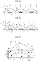
- the result of a simulation indicates that, when the angle of incidence of light with which a spherical lens and an asymmetric-aspherical lens are irradiated is changed with photoelectric cells respectively disposed below the lenses as shown in FIGS. 2A and 2B , the output of the photoelectric cell gradually decreases as the angle of incidence increases in the case of the spherical lens and in the case of the asymmetric-aspherical lens, the output of the photoelectric cell is approximately maintained until the angle of incidence reaches a certain degree (approximately 60° in illustrated example) even when the angle of incidence increases, as shown in FIG. 5 . Therefore, when the asymmetric-aspherical lens is used as a lens for light concentration in the photoelectric conversion device, it is possible to use light over a relatively wide range of angles for power generation of the photoelectric cells.
- the fluorescent light guide plate 2 carrying a fluorescent substance is used as a substrate on which the photoelectric cells 3 are mounted in order that light components missing the photoelectric cells can also be used for power generation and light with which the photoelectric cells 3 are not irradiated is concentrated by being converted into fluorescent light and can be used for power generation. Therefore, the power generation efficiency of the photoelectric conversion device can be improved.
- fluorescent substances 6 are dispersed inside the fluorescent light guide plate 2, on the upper surface of the fluorescent light guide plate 2, or on the lower surface of the fluorescent light guide plate 2 as described above and the fluorescent substances 6 are excited by the sunlight SL entering the fluorescent light guide plate 2 after missing the photoelectric cells 3 and emits fluorescent light FL.
- the fluorescent light FL from the fluorescent substances 6 is emitted from the fluorescent substances 6 in radial directions.
- the refractive index of the fluorescent light guide plate 2 is higher than the outside thereof, a part of the fluorescent light FL (FLxt, FLxb) is transmitted through the surfaces 2a, 2b of the fluorescent light guide plate 2 but a majority of components of the fluorescent light FL are confined inside the fluorescent light guide plate 2 due to reflection or total reflection, propagated to the edge surfaces 2e, and emitted by being concentrated to the edge surfaces 2e. Therefore, the photoelectric cell 5 is disposed on the edge surfaces 2e, and the photoelectric cell 5 is configured to absorb fluorescent light emitted from the edge surfaces 2e to generate power. A portion of sunlight entering the fluorescent light guide plate 2 may be concentrated to the edge surfaces 2e and absorbed by the photoelectric cell 5 to be converted into power as it is without being converted into fluorescent light.
- the photoelectric conversion device of the present embodiment when the photoelectric conversion device is disposed under the sunlight SL, first, the photoelectric cells 3 are irradiated with light concentrated at the lens portions 4a of the lens layer 4 and the light is converted into power at the photoelectric cells 3 and extracted to the outside through the power line 10a. Then, light components after incidence onto the lens layer 4 with which the photoelectric cells 3 are not irradiated are incident onto the fluorescent light guide plate 2 and converted into the fluorescent light FL by the fluorescent substances 6 at the fluorescent light guide plate 2.
- the fluorescent light FL is concentrated to the edge surfaces 2e of the fluorescent light guide plate 2, the photoelectric cell 5 is irradiated with the fluorescent light FL, and the fluorescent light FL is converted into power at the photoelectric cell 5 and extracted to the outside through the power line 10b.
- the device in the present embodiment improves robustness with respect to the angle of incidence of sunlight incident onto the lens layer 4.
- connection portion 4b is present between the lens portions 4a of the lens layer 4 that are adjacent to each other, the energy of sunlight entering the connection portion 4b is also converted into power and thus energy conversion efficiency is further improved. Therefore, with the device of the present embodiment, it is possible to extract, as power, sunlight components that reach the ground in the form of scattered light in addition to sunlight components that reach the ground in the form of direct light.
- the following improved configuration may be applied to the fluorescent light guide plate 2.
- a reflection mirror 8 that reflects light may be provided at the lower surface 2b of the fluorescent light guide plate 2 so that fluorescent light (or sunlight) is prevented from being emitted from the lower surface 2b of the fluorescent light guide plate 2.
- the reflection mirror for example, an aluminum film (refractive index 1.48), a silver film (refractive index 0.17), or a duralumin film (refractive index 1.48) may be adopted.
- a material having a refractive index lower than the refractive index of the fluorescent light guide plate 2 may be selected as the material of the reflection mirror 8 in order to reduce transmission of light through an interface between the fluorescent light guide plate 2 and the reflection mirror 8 as much as possible.
- a material having a refractive index lower than the refractive index of the fluorescent light guide plate 2 may be selected as the material of the lens layer 4 in order to prevent fluorescent light (or sunlight) from being emitted from the upper surface 2a of the fluorescent light guide plate 2.
- a material having a refractive index lower than the refractive index of the fluorescent light guide plate 2 and higher than the refractive index of the lens layer 4 may be selected as the material of the adhesive layer 7.
- the effect of confining light in the fluorescent light guide plate 2 is improved.
- the material of the adhesive layer 7 low-refractive-index epoxy (refractive index 1.50), cyanoacrylate (refractive index 1.43), acrylic adhesive (refractive index 1.49), or the like may be used.
- a layer having a refractive index lower than the refractive index of the lens layer 4 may be formed in a case where an adhesive layer 7a is applied between the photoelectric cells 3 and the fluorescent light guide plate 2.
- a reflection mirror 9 similar to the reflection mirror 8 may be disposed to prevent light from being emitted from a portion where no photoelectric cell 5 is installed. In this case, it is possible to reduce light that is emitted without being used for power generation at the edge surfaces of the fluorescent light guide plate 2.
- the fluorescent light wavelength and the absorption wavelength overlap with each other at least partially and in this case, fluorescent light emitted from the fluorescent substance 6 that has absorbed sunlight absorbed again by another fluorescent substance in some cases and energy loss due to the re-absorption occurs (energy of light converted into power is reduced).
- the fluorescent substance 6 needs to be provided at a portion in the fluorescent light guide plate 2 where the sunlight can reach and even in a case where the fluorescent substance 6 is present at a portion where the sunlight does not reach, the fluorescent substance 6 does not absorb the sunlight and merely absorbs fluorescent light emitted from other fluorescent substances 6, which is wasteful.
- the density or the amount of dispersal of the fluorescent substances in a portion where the sunlight does not reach may be lower than that in a portion where the sunlight can reach.
- a density L of the fluorescent substances in the above-described regions may be lower than a density H at other regions. Accordingly, the amount of re-absorption of fluorescent light performed by fluorescent substances that do not absorb sunlight is reduced and thus energy loss can be suppressed.
- reflection mirrors 8a may be locally disposed such that leakage of light from the surface 2b is suppressed as schematically illustrated in FIG. 4 .
Applications Claiming Priority (1)
| Application Number | Priority Date | Filing Date | Title |
|---|---|---|---|
| JP2020170813A JP7306359B2 (ja) | 2020-10-08 | 2020-10-08 | 太陽光発電のための光電変換装置 |
Publications (2)
| Publication Number | Publication Date |
|---|---|
| EP3982424A1 true EP3982424A1 (fr) | 2022-04-13 |
| EP3982424B1 EP3982424B1 (fr) | 2023-03-01 |
Family
ID=77367308
Family Applications (1)
| Application Number | Title | Priority Date | Filing Date |
|---|---|---|---|
| EP21191634.1A Active EP3982424B1 (fr) | 2020-10-08 | 2021-08-17 | Dispositif de conversion photoélectrique pour la génération photovoltaïque solaire |
Country Status (4)
| Country | Link |
|---|---|
| US (1) | US11456396B2 (fr) |
| EP (1) | EP3982424B1 (fr) |
| JP (1) | JP7306359B2 (fr) |
| CN (1) | CN114400265B (fr) |
Families Citing this family (1)
| Publication number | Priority date | Publication date | Assignee | Title |
|---|---|---|---|---|
| JP2023152536A (ja) | 2022-04-04 | 2023-10-17 | トヨタ自動車株式会社 | 車両の運転支援システム |
Citations (7)
| Publication number | Priority date | Publication date | Assignee | Title |
|---|---|---|---|---|
| JPS5849860A (ja) | 1981-09-18 | 1983-03-24 | Sanyo Electric Co Ltd | 太陽光エネルギ−変換器 |
| JP2014010251A (ja) | 2012-06-28 | 2014-01-20 | Sharp Corp | 二次レンズ、太陽電池実装体、集光型太陽光発電装置、および集光型太陽光発電モジュール |
| US8969715B2 (en) * | 2009-07-31 | 2015-03-03 | Peer+ B.V. | Luminescent optical device and solar cell system with such luminescent optical device |
| US20150214407A1 (en) * | 2013-06-13 | 2015-07-30 | Panasonic Intellectual Property Management Co., Ltd. | Condensing photoelectric conversion apparatus and system |
| KR20180001827A (ko) * | 2016-06-28 | 2018-01-05 | 엘지전자 주식회사 | 센싱장치 |
| US20190067505A1 (en) * | 2017-08-30 | 2019-02-28 | Korea Institute Of Science And Technology | Solar cell panel and the window comprising the same |
| JP2020513159A (ja) | 2017-04-06 | 2020-04-30 | エルジー エレクトロニクス インコーポレイティド | 太陽電池モジュール |
Family Cites Families (24)
| Publication number | Priority date | Publication date | Assignee | Title |
|---|---|---|---|---|
| JPH065783B2 (ja) * | 1986-06-26 | 1994-01-19 | 孝 堀米 | 蛍光型集光板を用いた高効率太陽光発電方法及びデバイス |
| JPH1079527A (ja) * | 1996-09-04 | 1998-03-24 | Toyota Motor Corp | 集光型太陽電池装置 |
| JP2003078156A (ja) * | 2001-09-06 | 2003-03-14 | Sharp Corp | 薄膜太陽電池及び集光反射素子 |
| JP2003101059A (ja) * | 2001-09-27 | 2003-04-04 | Sharp Corp | 薄膜太陽電池 |
| WO2006085397A1 (fr) * | 2005-02-09 | 2006-08-17 | Citizen Holdings Co., Ltd. | Plaque d’affichage pour appareil à cellule solaire et procédé de fabrication de plaque d’affichage pour appareil à cellule solaire |
| US20110308611A1 (en) * | 2010-03-19 | 2011-12-22 | Morgan Solar Inc. | Solar-light concentration apparatus |
| IL193701A (en) * | 2008-08-26 | 2015-01-29 | Renata Reisfeld | Glowing sun rays center |
| US9274266B2 (en) * | 2008-09-19 | 2016-03-01 | The Regents Of The University Of California | System and method for solar energy capture and related method of manufacturing |
| US20120240979A1 (en) * | 2010-01-13 | 2012-09-27 | Sharp Kabushiki Kaisha | Solar cell module and solar energy generating device |
| US20110253197A1 (en) * | 2010-02-17 | 2011-10-20 | Massachusetts Institute Of Technology | Tuned solar concentrators and devices and methods using them |
| JP2011233649A (ja) * | 2010-04-26 | 2011-11-17 | Sumitomo Electric Ind Ltd | 太陽電池モジュール、太陽光発電装置、および太陽光発電システム |
| CN102986036A (zh) * | 2010-06-15 | 2013-03-20 | 夏普株式会社 | 太阳能电池单元 |
| CN102947731B (zh) * | 2010-06-18 | 2016-01-20 | 株式会社尼康 | 聚光光学元件、聚光装置、光发电装置和光热转换装置 |
| US9306089B2 (en) * | 2010-11-11 | 2016-04-05 | Sharp Kabushiki Kaisha | Solar cell module and solar generator |
| WO2012141091A1 (fr) * | 2011-04-11 | 2012-10-18 | シャープ株式会社 | Dispositif de culture de plantes, dispositif de commande de culture, procédé de commande de culture et programme pour ceux-ci, et dispositif pour concevoir un dispositif de génération d'énergie solaire, procédé pour concevoir un dispositif de génération d'énergie solaire et programme pour ceux-ci |
| JP6053178B2 (ja) * | 2011-04-22 | 2016-12-27 | シャープ株式会社 | 太陽電池モジュールおよび太陽光発電装置 |
| JP2014139958A (ja) * | 2011-05-09 | 2014-07-31 | Sharp Corp | 太陽電池モジュールおよび太陽光発電装置 |
| JP2014232738A (ja) * | 2011-09-22 | 2014-12-11 | シャープ株式会社 | 太陽電池モジュールおよび太陽光発電装置 |
| CN104205620A (zh) | 2012-03-30 | 2014-12-10 | 夏普株式会社 | 二次透镜、太阳能电池安装体、聚光型太阳能发电单元、聚光型太阳能发电装置以及聚光型太阳能发电模块 |
| JP2014040380A (ja) * | 2012-08-21 | 2014-03-06 | Sharp Corp | 化合物、太陽電池モジュール及び太陽光発電装置 |
| JP2016062931A (ja) * | 2014-09-15 | 2016-04-25 | 国立大学法人長岡技術科学大学 | 集光型太陽電池モジュール及び集光型太陽光発電システム |
| CN106449844B (zh) * | 2016-10-20 | 2017-12-29 | 北京交通大学 | 太阳能光伏发电系统和制备方法 |
| KR101791130B1 (ko) * | 2016-11-18 | 2017-10-27 | 엘지전자 주식회사 | 태양전지 모듈 |
| US11011657B2 (en) * | 2017-10-11 | 2021-05-18 | Toyota Motor Engineering & Manufacturing North America, Inc. | Colored solar panels and structures comprising the same |
-
2020
- 2020-10-08 JP JP2020170813A patent/JP7306359B2/ja active Active
-
2021
- 2021-08-06 CN CN202110901238.1A patent/CN114400265B/zh active Active
- 2021-08-11 US US17/399,491 patent/US11456396B2/en active Active
- 2021-08-17 EP EP21191634.1A patent/EP3982424B1/fr active Active
Patent Citations (7)
| Publication number | Priority date | Publication date | Assignee | Title |
|---|---|---|---|---|
| JPS5849860A (ja) | 1981-09-18 | 1983-03-24 | Sanyo Electric Co Ltd | 太陽光エネルギ−変換器 |
| US8969715B2 (en) * | 2009-07-31 | 2015-03-03 | Peer+ B.V. | Luminescent optical device and solar cell system with such luminescent optical device |
| JP2014010251A (ja) | 2012-06-28 | 2014-01-20 | Sharp Corp | 二次レンズ、太陽電池実装体、集光型太陽光発電装置、および集光型太陽光発電モジュール |
| US20150214407A1 (en) * | 2013-06-13 | 2015-07-30 | Panasonic Intellectual Property Management Co., Ltd. | Condensing photoelectric conversion apparatus and system |
| KR20180001827A (ko) * | 2016-06-28 | 2018-01-05 | 엘지전자 주식회사 | 센싱장치 |
| JP2020513159A (ja) | 2017-04-06 | 2020-04-30 | エルジー エレクトロニクス インコーポレイティド | 太陽電池モジュール |
| US20190067505A1 (en) * | 2017-08-30 | 2019-02-28 | Korea Institute Of Science And Technology | Solar cell panel and the window comprising the same |
Non-Patent Citations (1)
| Title |
|---|
| T. MASUDA, SOLAR ENERGY, vol. 146, 2017, pages 523 - 531 |
Also Published As
| Publication number | Publication date |
|---|---|
| CN114400265A (zh) | 2022-04-26 |
| JP2022062642A (ja) | 2022-04-20 |
| EP3982424B1 (fr) | 2023-03-01 |
| US11456396B2 (en) | 2022-09-27 |
| US20220115550A1 (en) | 2022-04-14 |
| CN114400265B (zh) | 2023-12-15 |
| JP7306359B2 (ja) | 2023-07-11 |
Similar Documents
| Publication | Publication Date | Title |
|---|---|---|
| US8039731B2 (en) | Photovoltaic concentrator for solar energy system | |
| US4227939A (en) | Luminescent solar energy concentrator devices | |
| US4357486A (en) | Luminescent solar collector | |
| JP6416333B2 (ja) | 太陽電池モジュール | |
| JP2006313810A (ja) | 集光型太陽光発電装置 | |
| US20070227582A1 (en) | Low aspect ratio concentrator photovoltaic module with improved light transmission and reflective properties | |
| US8674281B2 (en) | Solar energy harvesting system using luminescent solar concentrator with distributed outcoupling structures and microoptical elements | |
| JP5624064B2 (ja) | 誘導放出ルミネッセンス光導波路太陽光集光器 | |
| KR101021587B1 (ko) | 건물 일체형 태양광 모듈 | |
| JPH0661519A (ja) | 反射鏡付き光電池モジュール | |
| US8354628B2 (en) | Luminescent solar concentrator with distributed outcoupling structures and microoptical elements | |
| US20130240037A1 (en) | Solar cell module and solar generator | |
| JP2006332113A (ja) | 集光型太陽光発電モジュール及び集光型太陽光発電装置 | |
| KR101762795B1 (ko) | 양면태양전지셀을 이용한 양면유리 태양전지 모듈과 입체형 반사체를 접목한 고효율 태양전지 시스템 | |
| EP3982424B1 (fr) | Dispositif de conversion photoélectrique pour la génération photovoltaïque solaire | |
| WO2013002093A1 (fr) | Dispositif de génération d'énergie photovoltaïque | |
| JP5929578B2 (ja) | 太陽電池モジュール及び太陽電池モジュール集合体 | |
| JP2007073774A (ja) | 太陽電池 | |
| WO2012128339A1 (fr) | Module de cellules solaires, dispositif de génération de puissance photovoltaïque et procédé d'installation de module de cellules solaires | |
| CN102709376A (zh) | 集有荧光平面光波导结构的太阳能电池组件用背板及应用 | |
| KR101898593B1 (ko) | 태양전지 모듈 | |
| JP2008311408A (ja) | 集光型太陽電池モジュール | |
| US8878050B2 (en) | Composite photovoltaic device with parabolic collector and different solar cells | |
| US20160284912A1 (en) | Photovoltaic cell | |
| KR101351249B1 (ko) | 광 분산렌즈를 구비하는 태양전지모듈 |
Legal Events
| Date | Code | Title | Description |
|---|---|---|---|
| PUAI | Public reference made under article 153(3) epc to a published international application that has entered the european phase |
Free format text: ORIGINAL CODE: 0009012 |
|
| STAA | Information on the status of an ep patent application or granted ep patent |
Free format text: STATUS: REQUEST FOR EXAMINATION WAS MADE |
|
| 17P | Request for examination filed |
Effective date: 20210902 |
|
| AK | Designated contracting states |
Kind code of ref document: A1 Designated state(s): AL AT BE BG CH CY CZ DE DK EE ES FI FR GB GR HR HU IE IS IT LI LT LU LV MC MK MT NL NO PL PT RO RS SE SI SK SM TR |
|
| GRAP | Despatch of communication of intention to grant a patent |
Free format text: ORIGINAL CODE: EPIDOSNIGR1 |
|
| STAA | Information on the status of an ep patent application or granted ep patent |
Free format text: STATUS: GRANT OF PATENT IS INTENDED |
|
| INTG | Intention to grant announced |
Effective date: 20220923 |
|
| GRAS | Grant fee paid |
Free format text: ORIGINAL CODE: EPIDOSNIGR3 |
|
| GRAA | (expected) grant |
Free format text: ORIGINAL CODE: 0009210 |
|
| STAA | Information on the status of an ep patent application or granted ep patent |
Free format text: STATUS: THE PATENT HAS BEEN GRANTED |
|
| AK | Designated contracting states |
Kind code of ref document: B1 Designated state(s): AL AT BE BG CH CY CZ DE DK EE ES FI FR GB GR HR HU IE IS IT LI LT LU LV MC MK MT NL NO PL PT RO RS SE SI SK SM TR |
|
| REG | Reference to a national code |
Ref country code: GB Ref legal event code: FG4D |
|
| REG | Reference to a national code |
Ref country code: CH Ref legal event code: EP Ref country code: AT Ref legal event code: REF Ref document number: 1551599 Country of ref document: AT Kind code of ref document: T Effective date: 20230315 |
|
| REG | Reference to a national code |
Ref country code: DE Ref legal event code: R096 Ref document number: 602021001514 Country of ref document: DE |
|
| REG | Reference to a national code |
Ref country code: IE Ref legal event code: FG4D |
|
| REG | Reference to a national code |
Ref country code: LT Ref legal event code: MG9D |
|
| REG | Reference to a national code |
Ref country code: NL Ref legal event code: MP Effective date: 20230301 |
|
| PG25 | Lapsed in a contracting state [announced via postgrant information from national office to epo] |
Ref country code: RS Free format text: LAPSE BECAUSE OF FAILURE TO SUBMIT A TRANSLATION OF THE DESCRIPTION OR TO PAY THE FEE WITHIN THE PRESCRIBED TIME-LIMIT Effective date: 20230301 Ref country code: NO Free format text: LAPSE BECAUSE OF FAILURE TO SUBMIT A TRANSLATION OF THE DESCRIPTION OR TO PAY THE FEE WITHIN THE PRESCRIBED TIME-LIMIT Effective date: 20230601 Ref country code: LV Free format text: LAPSE BECAUSE OF FAILURE TO SUBMIT A TRANSLATION OF THE DESCRIPTION OR TO PAY THE FEE WITHIN THE PRESCRIBED TIME-LIMIT Effective date: 20230301 Ref country code: LT Free format text: LAPSE BECAUSE OF FAILURE TO SUBMIT A TRANSLATION OF THE DESCRIPTION OR TO PAY THE FEE WITHIN THE PRESCRIBED TIME-LIMIT Effective date: 20230301 Ref country code: HR Free format text: LAPSE BECAUSE OF FAILURE TO SUBMIT A TRANSLATION OF THE DESCRIPTION OR TO PAY THE FEE WITHIN THE PRESCRIBED TIME-LIMIT Effective date: 20230301 Ref country code: ES Free format text: LAPSE BECAUSE OF FAILURE TO SUBMIT A TRANSLATION OF THE DESCRIPTION OR TO PAY THE FEE WITHIN THE PRESCRIBED TIME-LIMIT Effective date: 20230301 |
|
| REG | Reference to a national code |
Ref country code: AT Ref legal event code: MK05 Ref document number: 1551599 Country of ref document: AT Kind code of ref document: T Effective date: 20230301 |
|
| REG | Reference to a national code |
Ref country code: DE Ref legal event code: R084 Ref document number: 602021001514 Country of ref document: DE |
|
| PG25 | Lapsed in a contracting state [announced via postgrant information from national office to epo] |
Ref country code: SE Free format text: LAPSE BECAUSE OF FAILURE TO SUBMIT A TRANSLATION OF THE DESCRIPTION OR TO PAY THE FEE WITHIN THE PRESCRIBED TIME-LIMIT Effective date: 20230301 Ref country code: PL Free format text: LAPSE BECAUSE OF FAILURE TO SUBMIT A TRANSLATION OF THE DESCRIPTION OR TO PAY THE FEE WITHIN THE PRESCRIBED TIME-LIMIT Effective date: 20230301 Ref country code: NL Free format text: LAPSE BECAUSE OF FAILURE TO SUBMIT A TRANSLATION OF THE DESCRIPTION OR TO PAY THE FEE WITHIN THE PRESCRIBED TIME-LIMIT Effective date: 20230301 Ref country code: GR Free format text: LAPSE BECAUSE OF FAILURE TO SUBMIT A TRANSLATION OF THE DESCRIPTION OR TO PAY THE FEE WITHIN THE PRESCRIBED TIME-LIMIT Effective date: 20230602 Ref country code: FI Free format text: LAPSE BECAUSE OF FAILURE TO SUBMIT A TRANSLATION OF THE DESCRIPTION OR TO PAY THE FEE WITHIN THE PRESCRIBED TIME-LIMIT Effective date: 20230301 |
|
| REG | Reference to a national code |
Ref country code: GB Ref legal event code: 746 Effective date: 20230922 |
|
| PG25 | Lapsed in a contracting state [announced via postgrant information from national office to epo] |
Ref country code: SM Free format text: LAPSE BECAUSE OF FAILURE TO SUBMIT A TRANSLATION OF THE DESCRIPTION OR TO PAY THE FEE WITHIN THE PRESCRIBED TIME-LIMIT Effective date: 20230301 Ref country code: RO Free format text: LAPSE BECAUSE OF FAILURE TO SUBMIT A TRANSLATION OF THE DESCRIPTION OR TO PAY THE FEE WITHIN THE PRESCRIBED TIME-LIMIT Effective date: 20230301 Ref country code: PT Free format text: LAPSE BECAUSE OF FAILURE TO SUBMIT A TRANSLATION OF THE DESCRIPTION OR TO PAY THE FEE WITHIN THE PRESCRIBED TIME-LIMIT Effective date: 20230703 Ref country code: EE Free format text: LAPSE BECAUSE OF FAILURE TO SUBMIT A TRANSLATION OF THE DESCRIPTION OR TO PAY THE FEE WITHIN THE PRESCRIBED TIME-LIMIT Effective date: 20230301 Ref country code: CZ Free format text: LAPSE BECAUSE OF FAILURE TO SUBMIT A TRANSLATION OF THE DESCRIPTION OR TO PAY THE FEE WITHIN THE PRESCRIBED TIME-LIMIT Effective date: 20230301 Ref country code: AT Free format text: LAPSE BECAUSE OF FAILURE TO SUBMIT A TRANSLATION OF THE DESCRIPTION OR TO PAY THE FEE WITHIN THE PRESCRIBED TIME-LIMIT Effective date: 20230301 |
|
| P01 | Opt-out of the competence of the unified patent court (upc) registered |
Effective date: 20231024 |
|
| PG25 | Lapsed in a contracting state [announced via postgrant information from national office to epo] |
Ref country code: SK Free format text: LAPSE BECAUSE OF FAILURE TO SUBMIT A TRANSLATION OF THE DESCRIPTION OR TO PAY THE FEE WITHIN THE PRESCRIBED TIME-LIMIT Effective date: 20230301 Ref country code: IS Free format text: LAPSE BECAUSE OF FAILURE TO SUBMIT A TRANSLATION OF THE DESCRIPTION OR TO PAY THE FEE WITHIN THE PRESCRIBED TIME-LIMIT Effective date: 20230701 |
|
| PGFP | Annual fee paid to national office [announced via postgrant information from national office to epo] |
Ref country code: FR Payment date: 20230703 Year of fee payment: 3 Ref country code: DE Payment date: 20230627 Year of fee payment: 3 |
|
| REG | Reference to a national code |
Ref country code: DE Ref legal event code: R097 Ref document number: 602021001514 Country of ref document: DE |
|
| PLBE | No opposition filed within time limit |
Free format text: ORIGINAL CODE: 0009261 |
|
| STAA | Information on the status of an ep patent application or granted ep patent |
Free format text: STATUS: NO OPPOSITION FILED WITHIN TIME LIMIT |
|
| PG25 | Lapsed in a contracting state [announced via postgrant information from national office to epo] |
Ref country code: SI Free format text: LAPSE BECAUSE OF FAILURE TO SUBMIT A TRANSLATION OF THE DESCRIPTION OR TO PAY THE FEE WITHIN THE PRESCRIBED TIME-LIMIT Effective date: 20230301 Ref country code: DK Free format text: LAPSE BECAUSE OF FAILURE TO SUBMIT A TRANSLATION OF THE DESCRIPTION OR TO PAY THE FEE WITHIN THE PRESCRIBED TIME-LIMIT Effective date: 20230301 |
|
| 26N | No opposition filed |
Effective date: 20231204 |
|
| PG25 | Lapsed in a contracting state [announced via postgrant information from national office to epo] |
Ref country code: MC Free format text: LAPSE BECAUSE OF FAILURE TO SUBMIT A TRANSLATION OF THE DESCRIPTION OR TO PAY THE FEE WITHIN THE PRESCRIBED TIME-LIMIT Effective date: 20230301 |
|
| PG25 | Lapsed in a contracting state [announced via postgrant information from national office to epo] |
Ref country code: MC Free format text: LAPSE BECAUSE OF FAILURE TO SUBMIT A TRANSLATION OF THE DESCRIPTION OR TO PAY THE FEE WITHIN THE PRESCRIBED TIME-LIMIT Effective date: 20230301 |
|
| PG25 | Lapsed in a contracting state [announced via postgrant information from national office to epo] |
Ref country code: LU Free format text: LAPSE BECAUSE OF NON-PAYMENT OF DUE FEES Effective date: 20230817 |