EP3979274A1 - Induktives gerüst, induktive vorrichtung und lampe - Google Patents
Induktives gerüst, induktive vorrichtung und lampe Download PDFInfo
- Publication number
- EP3979274A1 EP3979274A1 EP20867268.3A EP20867268A EP3979274A1 EP 3979274 A1 EP3979274 A1 EP 3979274A1 EP 20867268 A EP20867268 A EP 20867268A EP 3979274 A1 EP3979274 A1 EP 3979274A1
- Authority
- EP
- European Patent Office
- Prior art keywords
- end plate
- conductive welding
- connection surface
- main winding
- welding components
- Prior art date
- Legal status (The legal status is an assumption and is not a legal conclusion. Google has not performed a legal analysis and makes no representation as to the accuracy of the status listed.)
- Granted
Links
Images


Classifications
-
- H—ELECTRICITY
- H01—ELECTRIC ELEMENTS
- H01F—MAGNETS; INDUCTANCES; TRANSFORMERS; SELECTION OF MATERIALS FOR THEIR MAGNETIC PROPERTIES
- H01F27/00—Details of transformers or inductances, in general
- H01F27/28—Coils; Windings; Conductive connections
- H01F27/30—Fastening or clamping coils, windings, or parts thereof together; Fastening or mounting coils or windings on core, casing, or other support
- H01F27/306—Fastening or mounting coils or windings on core, casing or other support
-
- H—ELECTRICITY
- H01—ELECTRIC ELEMENTS
- H01F—MAGNETS; INDUCTANCES; TRANSFORMERS; SELECTION OF MATERIALS FOR THEIR MAGNETIC PROPERTIES
- H01F17/00—Fixed inductances of the signal type
- H01F17/04—Fixed inductances of the signal type with magnetic core
- H01F17/06—Fixed inductances of the signal type with magnetic core with core substantially closed in itself, e.g. toroid
- H01F17/062—Toroidal core with turns of coil around it
-
- H—ELECTRICITY
- H01—ELECTRIC ELEMENTS
- H01F—MAGNETS; INDUCTANCES; TRANSFORMERS; SELECTION OF MATERIALS FOR THEIR MAGNETIC PROPERTIES
- H01F27/00—Details of transformers or inductances, in general
- H01F27/06—Mounting, supporting or suspending transformers, reactors or choke coils not being of the signal type
-
- H—ELECTRICITY
- H01—ELECTRIC ELEMENTS
- H01F—MAGNETS; INDUCTANCES; TRANSFORMERS; SELECTION OF MATERIALS FOR THEIR MAGNETIC PROPERTIES
- H01F27/00—Details of transformers or inductances, in general
- H01F27/24—Magnetic cores
-
- H—ELECTRICITY
- H01—ELECTRIC ELEMENTS
- H01F—MAGNETS; INDUCTANCES; TRANSFORMERS; SELECTION OF MATERIALS FOR THEIR MAGNETIC PROPERTIES
- H01F27/00—Details of transformers or inductances, in general
- H01F27/24—Magnetic cores
- H01F27/26—Fastening parts of the core together; Fastening or mounting the core on casing or support
- H01F27/263—Fastening parts of the core together
-
- H—ELECTRICITY
- H01—ELECTRIC ELEMENTS
- H01F—MAGNETS; INDUCTANCES; TRANSFORMERS; SELECTION OF MATERIALS FOR THEIR MAGNETIC PROPERTIES
- H01F27/00—Details of transformers or inductances, in general
- H01F27/28—Coils; Windings; Conductive connections
- H01F27/2823—Wires
-
- H—ELECTRICITY
- H01—ELECTRIC ELEMENTS
- H01F—MAGNETS; INDUCTANCES; TRANSFORMERS; SELECTION OF MATERIALS FOR THEIR MAGNETIC PROPERTIES
- H01F27/00—Details of transformers or inductances, in general
- H01F27/28—Coils; Windings; Conductive connections
- H01F27/2823—Wires
- H01F27/2828—Construction of conductive connections, of leads
-
- H—ELECTRICITY
- H01—ELECTRIC ELEMENTS
- H01F—MAGNETS; INDUCTANCES; TRANSFORMERS; SELECTION OF MATERIALS FOR THEIR MAGNETIC PROPERTIES
- H01F27/00—Details of transformers or inductances, in general
- H01F27/06—Mounting, supporting or suspending transformers, reactors or choke coils not being of the signal type
- H01F2027/065—Mounting on printed circuit boards
Definitions
- the present disclosure relates to the technical field of inductor manufacture, especially to an inductor framework, an inductor device and a lamp.
- An inductor is an element able to convert electric energy into magnetic energy to store the magnetic energy, and is widely applied in various electronic products in many fields such as aerospace, signal communication and household electric appliances, etc.
- the inductor consists generally of a framework, windings, a shielding case, packaging materials, magnetic cores, iron cores, etc.
- inductor devices applicable to patch assembly technology usually use a winding post protruding from sides of an inductor framework and a wire head of the inductor is wound on the winding post to form a welding winding.
- the welding winding can be directly bonded and welded with a bonding pad on a circuit board, so as to complete the fixation and electrical connection between the inductor device and the circuit board.
- the patch type assembly of the inductor device and the circuit board can be achieved by the above methods, but in order to further enhance the product competitiveness, it is necessary to make a further miniaturized improvement of the inductor device.
- At least one embodiment of the present disclosure provides an inductor framework, an inductor device and a lamp to solve the above problem.
- At least one embodiment of the present disclosure adopts the following technical schemes.
- At least one embodiment of the present disclosure provides an inductor framework, the inductor framework comprises a main winding part and at least two conductive welding components; the main winding is configured to fix a winding and has a connection surface facing downward, the conductive welding components are under the connection surface and at least partly cover the connection surface, and the conductive welding components are in fixed connection with the main winding part and the at least two conductive welding components are insulated from each other; and side surface of the conductive welding components away from the connection surface is a welding bonding surface, and the conductive welding components have a wire accommodation region, and the wire accommodation region is configured that a wire of the winding do not extend beyond the welding bonding surface in a case where the wire of the winding is accommodated in the wire accommodation region.
- connection surface is separated into two portions by a separation band, and the conductive welding components are divided into two parts corresponding to the two portions of the connection surface, the two parts of the conductive welding components are respectively provided on the two portions of the connection surface, and the different two parts of the conductive welding components are insulated from each other.
- connection surface is separated into a plurality of portions by a plurality of separation bands intersecting each other, and the conductive welding components are divided correspondingly into a plurality of parts corresponding to the plurality of portions of the connection surface, plurality of parts of the conductive welding components are respectively provided on the plurality of portions of the connection surface in a one-to-one correspondence manner, and different parts of the plurality of parts of the conductive welding components are insulated from each other.
- the main winding part has a main winding post, a first end plate and a second end plate, the main winding part is between the first end plate and the second end plate, both an edge of the first end plate and an edge of the second end plate extend beyond the main winding post, and the first end plate and the second end plate together with the main winding post constitute a main winding groove.
- an axis of the main winding post is vertical to a horizontal plane, and a downward side surface of the fist end plate is the connection surface.
- the first end plate is provided with a separation boss which protrudes downward from a middle portion of the connection surface and separates the connection surface into two portions, each portion of the connection surface is provided with one part of the conductive welding components, and the welding bonding surface extend beyond the separation boss or is flush with the separation boss.
- the first end plate is provided with a first embedding part configured to be embedded into a first magnetic core, and the conductive welding components are divided into two parts which are respectively provided on two sides of the first embedding part.
- an axis of the main winding post is parallel to a horizontal plane, and both a downward side surface of the first end plate and a downward side surface of the second end plate are the connection surface, one part of the conductive welding components is under the first end plate, and other part of the conductive welding components is under of the second end plate.
- the first end plate is provided with a first embedding part configured to be embedded into a first magnetic core
- the second end plate is provided with a second embedding configured to be embedded into a second magnetic core
- the first embedding part separates a part of the connection surface of the first end plate into two opposite portions
- the second embedding part separates a part of the connection surface of the second end plate into two opposite portions
- each part of the connection surface is covered with a part of the conductive welding components and the part of the conductive welding components is under the each part of the connection surface.
- the wire accommodation region is a wire groove provided on the welding bonding surface.
- the main winding part has a receiving cavity which is recessed inwardly from the connection surface and is configured to fix the winding, and the conductive welding components surround the receiving cavity.
- the wire accommodation region is a wire groove provided on the welding bonding surface.
- the wire groove is a gradually widening structure which is gradually widen from a bottom of the groove to an opening of the groove.
- the wire groove passes across two opposite sides of the conductive welding components.
- the main winding part is further provided with a limit groove, an end of the limit groove extends into the wire groove.
- the conductive welding components cover an entirety of the connection surface, and the conductive welding components are further provided with a wire passage channel interconnecting the wire groove and the limit groove.
- the wire passage channel is a wire passage hole or a wire passage notch.
- each of the conductive welding components is a sheet structure.
- the conductive welding components is attached to the connecting surface or is hot-melt connected with the connection surface.
- a bottom of the main winding part is provided with an area extension part, and the connection surface is a downward surface of the area extension part.
- At least one embodiment of the present disclosure provides an inductor device, the inductor device comprises a winding and the above-mentioned inductor framework; and the winding is constituted by winding a wire with an insulating sheath, has an input wire and an output wire, and the winding is fixed on the main winding part, and the input wire and the output wire are respectively accommodated in the wire accommodation region of two of the at least two conductive welding components insulated from each other.
- the main winding part in a case where the main winding part has a main winding post, a first end plate and a second end plate, the main winding part is between the first end plate and the second end plate, both an edge of the first end plate and an edge of the second end plate extend beyond the main winding post, and the first end plate and the second end plate together with the main winding post constitute a main winding groove, the winding is wound in the main winding groove.
- the main winding part is made of a magnetic material.
- the main winding part is made of a nonmagnetic material
- the inductor device further comprises a first magnetic core and a second magnetic core, with the first magnetic core is buckled on the first end plate and the second magnetic core is buckled on the second end plate.
- a through insertion hole is provided in the main winding post, the first end plate is provided with a first embedding part configured to be embedded into a magnetic core, and the second end plate is provided with a second embedding part configured to be embedded into a magnetic core, with the insertion hole communicating with the first embedding part and the second embedding part; and the first magnetic core is embedded into the first embedding part and a part of the first magnetic core extends into the insertion hole, and a part of the second magnetic core is embedded into the second embedding part and a part of the second magnetic core extends into the insertion hole.
- both the first magnetic core and the second magnetic core are in a shape of E
- a middle extension portion of the shape of E is a center column
- the center column of the first magnetic core and the center column of the first magnetic core both extend into the insertion hole.
- the wire with an insulation sheath is any one selected from a group consisting of a flat wire, an enameled wire, a multi-strand wire, a three-layer wire and a silk-covered wire.
- the inductor device in a case where the main winding part has a receiving cavity which is recessed inwardly from the connection surface and is configured to fix the winding, and the conductive welding components surround the receiving cavity, the inductor device further comprises an annular magnetic core, the winding is wound on the annular magnetic core, and the annular magnetic core and the winding are both fixed in the receiving cavity.
- At least one embodiment of the present disclosure provides a lamp, the lamp comprises a lamp body, a light source module and a driver module; the light source module and the driver module are both provided on the lamp body and electrically connected to each other, the driver module comprises a circuit board, and the and which is provided with the above-mentioned inductor device.
- the inductor framework, the inductor device and the lamp provided in the embodiments of the present disclosure can reduce significantly the area occupied by the inductor device, by the connection surface of the main winding part being covered with the conductive welding components, accommodating the wires and being bonded with the circuit board.
- an inductor device which can be applied in various lighting lamp products, such as LED lighting products, for example, downlights, bulbs, lighting modules, ceiling lamps, street lamps, and mining lamps, etc.
- the inductor device can be applied in other products in the electronic field.
- a lamp product usually includes a lamp body, a light source module and a driver module, the light source module and the driver module are both provided on the lamp body and electrically connected to each other.
- the light source module is configured to emit illumination light
- the driver module is configured to drive the light source module
- the driver module includes a circuit board
- the inductor device is provided on the circuit board.
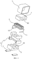
- the inductor device may include a first magnetic core 4, a second magnetic core 5 and a reinforcement tape 5.
- the inductor framework 1 in the embodiment includes a main winding part 10 and at least two conductive welding components 11, and specifically, the main winding part 10 may be made of an insulation material.
- the main winding part 10 is configured to fix the winding 2, and the winding 2 may be formed by winding a wire with an insulation sheath such as a flat wire, enameled wire, multi-strand wire, three-layer wire or silk-covered wire.
- the main winding part 10 further has a downward connection surface 106.
- the connection surface 106 is originally a surface for connecting a PCB board so that it should be located at the lowest position of the main winding part 10.
- the conductive welding components 11 are under the connection surface 106 and partly cover the connection surface 106, and are fixedly connected with the main winding part 10.
- the conductive welding components 11 may be directly connected with the connection surface 106 by means of pasting, hot melting, etc., or may cover (or referred to as "be fixed to") the surface 106 and under the surface 106 by fixedly connecting with other parts of the main winding part 10. Namely, the conductive welding components 11 replace the position of the original connection surface 106 to be connected with the PCB board. All the conductive welding components 11 may be under the connection surface 106.
- connection surface 106 it may be necessary for the conductive welding components 11 to extend partly beyond a range of projections of the connection surface 106 and the main winding 10 due to a small area of the connection surface 106, but not to usually extend too much beyond the range of the projections of the connection surface 106 and the main winding 10 because some regions under the connection surface 106 can be used.
- an area extension parts 105 ( FIG.5 , 8 and 14 ) with a larger area can be formed on a bottom of the main winding part 10 to expand the area of the connection surface 106, so that it can be ensured that all the conductive welding components 11 can still be under the connection surface 106, which will be exemplified below.
- a side of the conductive welding components 11 away from the connection surface 106 is a welding bonding surface 110, that is, the surface for bonding and welding with the PCB board.
- a welding bonding surface 110 that is, the surface for bonding and welding with the PCB board.
- at least one of the conductive welding components 11 is provided with a wire accommodation region 111, there is a certain requirement for the accommodation region 111 in size in the embodiment, namely, the size of the accommodation region 111 is required that a wire of the winding 2 do not extend beyond the welding bonding surface 110 when the wire of the winding 2 is accommodated within the wire accommodation region 111.
- the wire accommodation region 111 in the embodiment is a through hole or other structures without extending to the welding bonding surface 110, and in this case the wire accommodation region 111 can adopt any form of structure able to accommodate the wires, which will not cause the wires to extend beyond the welding bonding surface 110.
- the wire accommodation region 111 in the embodiment may be a wire groove provided on the welding bonding surface 110.
- the wire groove 111 (for ease of description, the reference numeral of the wire accommodation region is used below) has a depth at least equal to a diameter of the wire.
- the wire groove 111 is more convenient for the wire to enter because the wire groove 111 is an open structure, and the wire groove 111 may accommodate tin solder in addition to the wire, thus obtaining a better welding effect.
- the wire groove 111 can be designed to have a gradual widening structure which is gradual widen from a bottom 111b of the groove 111 to an opening 111a of the groove 111, for example, a cross section of the wire groove 111 is gradual widening structures in various possible shapes, such as Semicircle, trapezoid, triangle, trumpet shape, etc.
- this type of gradual widening structure can lead the wire to the bottom of the groove with a smaller width to position the wire, and on the other hand, can accommodate more tin solder and have a larger solder contact surface to facilitate improving the welding effect.
- the wire groove 111 may pass across two opposite sides of the corresponding conductive welding component 11, and an extension direction of the wire groove 111 may be designed according to a direction in which the wire of the winding 2 is led out or may be oriented at any direction.
- the wire passes through the wire groove 11 in cooperation with the extension direction of the wire groove 11.
- the main winding part 10 may be provided with a limit groove 104 which extend from the main winding part 10 to the wire groove 111.
- the wire can extend along the limit groove 104 from the main winding part 10 to the wire groove 111 of the corresponding conductive welding component 11. After the winding operation is completed, this segment of the wire is limited in the limit groove 104 and cannot move freely, thus avoiding the relaxation of the winding 2.
- the conductive welding components 11 usually cover the entire region of the connection surface.
- the wires need to pass over the upper parts of the conductive welding component 11 through a relatively rapid bend to reach the wire groove 111 located on the welding bonding surface 110.
- the wire has a particularly large bending amplitude, which is inconvenient to assembling the wire. Therefore, as shown in FIG. 2 and FIG.
- each conductive welding components 11 is further provided with a wire passage channel 112 which interconnect the wire groove 111 and the limit groove 104, and the wire passage channel 112 may be a wire passage hole or a notch provided on the corresponding conductive welding component 11.
- the entire inductor device can be welded on the PCB board through the conductive welding components 11 and at the same time the winding 2 can also be connected to a circuit of the PCB board through the conductive welding components 11. It is necessary for a positive terminal and a negative terminal of the winding 2 to be simultaneously connected to the circuit, so that it is required that the positive and negative terminals are respectively connected to the circuit through different conductive welding components 11 in order to prevent a short circuit. Therefore, in the embodiment, at least two of the conductive welding components 11 are insulated from each other when they are provided. The two conductive welding components 11 are respectively used for electrically connecting the input wire 20 and the output wire 21 of the winding 2 so as to smoothly connect the winding 2 to the circuit.
- an area occupied by the inductor device is that occupied by the conductive welding components 11, and the conductive welding components 11 can use a part of the area or space under the connection surface 106, so that the area occupied by the inductor device is reduced significantly. Therefore, the area of the occupied circuit board is saved, so that the circuit board has a more compact structure or other necessary components are arranged to reduce costs.
- connection surface 106 may be separated into two portions by a separation band, and at the same time the conductive welding components 11 are also divided into two parts corresponding to the two portions of the connection surface.
- Each portion of the connection surface 106 is provided with a part of conductive welding components 11, and the conductive welding components 11 located on different portions of the connection surface 106 may be spaced by a long distance to be insulated from each other.
- the input wire 20 of the winding 2 and the output wire 21 of the winding 2 are respectively electrically connected with the conductive welding components 11 on different sides from two opposite sides, which can be easily performed.
- the separation band may be an entity, and for example, the connection surface 106 may be truly separated into two portions through a structure such as a groove, a hole or a boss on the connection surface 106.
- the separation band may be fictional, and the actual connection surface 106 is still an integral structure.
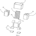
- the main winding part 10 can have a main winding post 101, a first end plate 102 and a second end plate 103, the main winding post 101 is between the first end plate 102 and the second end plate 103.
- An edge of the first end plate 102 and an edge of the second end plate 103 are both extend beyond the main winding post 101, and the first end plate 102 and the second end plate 103 together with the main winding post 101 constitute a main winding groove 100, the winding 2 is wound in the main winding groove 100.
- the main winding part 10 may be made of a nonmagnetic material, and in order to reduce costs, it is recommended to use phenolic plastic as the material of the main winding part 10.
- the first end plate 102 may be provided with a first embedding part 102a configured to be embedded into a first magnetic core 3
- the second end plate 103 can be provided with a second embedding part 103a configured to be embedded into a second magnetic core 4.
- the main winding post 101 can further be provided with a through insertion hole 101a which passes through the main winding post 101, and the through insertion hole 101a communicates with the first embedding part 102a and the second embedding part 103a.
- the first magnetic core 3 is embedded into the first embedding part 102a, a part of the first magnetic core 3 extends into the insertion hole 101a.
- the first magnetic core 3 is in a shape of E
- a middle extension portion of the shape of E is a center column 30, and the center column 30 extends into the insertion hole 101a.
- a part of the second magnetic core 4 is embedded into the second embedding part 103a, and another part of the second magnetic core 4 also extends into the insertion hole 101a.
- the second magnetic core 4 also in a shape of E, a middle extension portion of the shape of E is a center column 40, and the center column 40 extends into the insertion hole 101a.
- Extension portions on two sides of the first magnetic core 3 and the second magnetic core 4 are aligned to cover the periphery of the windings 2.
- the reinforcement tape 5 can be wound around peripheries of the first magnetic core 3 and the second magnetic core 4 to fix them.
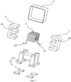
- the inductor device can be classified into a vertical inductor device or a horizontal device in accordance with different axis directions of the main winding post 101.
- an axis of the main winding post 101 of the inductor framework 1 is vertical to a horizontal plane, the first end plate 102 is located on a bottom of the main winding post 101, and the second end plate 103 is located on a top of the main winding post 103, with a downward side of the first end plate 102 being the connection surface 106.
- two parts of conductive welding components 11 are respectively provided on two opposite sides under the first end plate 102. As shown in FIG. 2 and FIG.
- the first embedding part 102a may be just used as a marker, so that the connection surface 106 can be separated into two portions using the first embedding part 102a as the separation band, and the two parts of conductive welding components 11 can be respectively provided on two sides of the first embedding part 102a.
- the first embedding part 102a can be a structure such as a groove to partially separate the connection surface 106 or even completely separate the connection surface 106 into two independent portions.
- a size of the first end plate 102 may be larger as a whole, so that the first end plate 102 has a larger area than the second end plate 103 to bear the conductive welding components 11.
- an axis of the main winding post 101 is parallel to the horizontal plane, and the first end plate 102 and the second end plate 103 are respectively located on a left side of the main winding post 101 and a right side of the main winding post 101, with a downward side surface of the first end plate 102 and a downward side surface of the second end plate 103 both used as the connection surface 106.
- the first end plate 102 and the second end plate 103 are separated by the main winding post 101, so that the two portions of the connection surface 106 located respectively on the first end plate 102 and the second end plate 103 themselves are regarded as two independent portions separated by a first separation band.
- the two parts of conductive welding components 11 can be accordingly insulated from each other.
- the bottom of the first end plate 102 and the bottom of the second end plate 103 are respectively provided with an area extension part 105 to increase the size of the connection surface in the axis direction of the main winding post 101, thus increasing the area of the connection surface.
- the inductor framework 1 it is necessary for the inductor framework 1 to adapt to different types of windings 2, the input wire 20 and the output wire 21 of each type of winding 2 that are led out have different led out locations, and therefore, for the input wire 20 and the output wire 21 not to need excessively long conveying paths, the conductive welding components 11 are provided at a plurality of angles in the inductor framework 1.
- connection surface 106 can be separated into a plurality of portions by a plurality of intersection separation bands, and at the same time, the conductive welding components 11 are also correspondingly divided into a plurality of parts corresponding to the plurality of portions of the connection surface.
- Each portion of the connection surface 106A is provided respectively with one part of conductive welding components 11, and different parts of the plurality of parts of the conductive welding components 11 are insulated from each other. In this way, there are conductive welding components 11 available in sufficient quantity and orientation, so that the inductor framework 1 has a better versatility.
- the first magnetic core 3 and the second magnetic core 4 because there are two ways to buckle the first magnetic core 3 and the second magnetic core 4. One way is to buckle them along the horizontal plane (see FIGS. 4-6 ), without the magnetic cores to pass across the bottom of the main winding part 10. The other way is to buckle them along a vertical plane (see FIGS. 7-9 ), by which the magnetic cores still need to pass across the bottom of the main winding part 10, so that it is necessary that the first embedding part 102a and the second embedding part 103a respectively extend to the bottom of the first end plate 102 and the bottom of the second end plate 103. On this basis, the first embedding part 102a and the second embedding part 103a can be used as a second separation band intersecting the first separation band.
- the first embedding part 102a is one portion of the second separation band and is used to separate the portion of the connection surface 106 on the first end plate 102 into two opposite portions again, and at the same time, the second embedding part 103a is the other portion of the second separation band and is used to separate the portion of the connection surface 106 on the second end plate 103 into two opposite portions again.
- the connection surface 106 is separated into four portions in total, and each portion of the connection surface 106 is covered with the conductive welding component 11 and the conductive welding component 11 is under the respective portion of the connection surface 106.
- each portion of the connection surface 106 is provided with an area extension part 105 which extends beyond the first end plate 102 and the second end plate 103 along both the axis direction of the main winding post 101 and a direction vertical to the axis, so that a larger connection surface can be obtained to bear the conductive welding components 11.
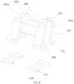
- the main winding post 10 in the embodiment may be made of a magnetic material, with an additional magnetic core omitted from the whole inductor device.
- the first end plate 102 may be provided with a separation boss 107 protruding downward from a middle portion of the connection surface 106.
- the separation boss 107 can separate the connection surface 106 into two portions, each portion of the connection surface 106 is provided respectively with one part of conductive welding components 11, so that the conductive welding components 11 located on different portions of the connection surface 106 can be separated accordingly to be insulated from each other.
- the separation boss 107 cannot protrude from the connection surface 106 too much, in order to ensure that the welding bonding surface 110 extends beyond the separation boss 107 or is flush with the separation boss 107 to meet the welding requirements.
- the main winding part 10 may have a receiving cavity 108 which is which is recessed inwardly from the connection surface 106 and is configured to fix the winding 2.
- the conductive welding components 11 are provided on the connection surface 106 around the receiving cavity 108.
- the inductor device further includes an annular magnetic core 6, the winding 2 is wound on the annular magnetic core 6, and the annular magnetic core 6 and the winding 2 are then fixed in the receiving cavity 106 together.
- annular magnetic core 6 On same annular magnetic core 6 can be wound one winding 2 or can also be simultaneously wound a plurality of windings 2.
- the annular magnetic core 6 and the winding 2 can be fixed in the receiving cavity 108 by means of clamping, gluing, etc.
- the receiving cavity 108 has a circular contour
- the main winding part 10 may have an overall outer contour which is a regular quadrangular prism structure, a regular octagonal prism structure or other prismatic structures that use the connection surface 106 as the bottom.
- connection surface 106 is usually a narrow circle surrounding the receiving cavity 108 and has a limited area, so that the area extension part 105 may be provided at different positions around the receiving cavity 108 to expand the area of the connection surface 106 by referring to the above embodiments.
- the main winding part 10 may be made of not only a non-magnetic material but also a magnetic shielding material. In the case where the main winding part 10 is made of the magnetic shielding material, a good magnetic shielding effect can be achieved, thus reducing the magnetic interference of the inductor device on other surrounding components.
- the inductor framework, the inductor device, and the lamp provided in the embodiments of the present disclosure can greatly reduce the area occupied by the inductor device.
Landscapes
- Engineering & Computer Science (AREA)
- Power Engineering (AREA)
- Microelectronics & Electronic Packaging (AREA)
- Coils Or Transformers For Communication (AREA)
Applications Claiming Priority (3)
| Application Number | Priority Date | Filing Date | Title |
|---|---|---|---|
| CN201910906703.3A CN110517868B (zh) | 2019-09-24 | 2019-09-24 | 电感骨架、电感装置及灯具 |
| CN201921599871.4U CN210272031U (zh) | 2019-09-24 | 2019-09-24 | 电感骨架、电感装置及灯具 |
| PCT/CN2020/115510 WO2021057566A1 (zh) | 2019-09-24 | 2020-09-16 | 电感骨架、电感装置及灯具 |
Publications (3)
| Publication Number | Publication Date |
|---|---|
| EP3979274A1 true EP3979274A1 (de) | 2022-04-06 |
| EP3979274A4 EP3979274A4 (de) | 2022-10-26 |
| EP3979274B1 EP3979274B1 (de) | 2024-03-20 |
Family
ID=75165605
Family Applications (1)
| Application Number | Title | Priority Date | Filing Date |
|---|---|---|---|
| EP20867268.3A Active EP3979274B1 (de) | 2019-09-24 | 2020-09-16 | Induktives gerüst, induktive vorrichtung und lampe |
Country Status (3)
| Country | Link |
|---|---|
| US (1) | US12347609B2 (de) |
| EP (1) | EP3979274B1 (de) |
| WO (1) | WO2021057566A1 (de) |
Families Citing this family (3)
| Publication number | Priority date | Publication date | Assignee | Title |
|---|---|---|---|---|
| KR20230005462A (ko) * | 2021-07-01 | 2023-01-10 | 엘지이노텍 주식회사 | 안정적인 내전압 특성을 갖는 슬림형 자기 결합 장치 |
| CN114914068B (zh) * | 2022-05-30 | 2026-02-17 | 英飞特电子(杭州)股份有限公司 | 一种磁性装置 |
| CN119049842B (zh) * | 2024-09-14 | 2025-11-25 | 东莞顺络功率器件有限公司 | 磁性器件及其制备方法 |
Family Cites Families (24)
| Publication number | Priority date | Publication date | Assignee | Title |
|---|---|---|---|---|
| DE3232533A1 (de) * | 1981-09-04 | 1983-05-05 | Toko, Inc., Tokyo | Chip-spule |
| JPH09148148A (ja) * | 1995-11-17 | 1997-06-06 | Toko Inc | インダクタンス素子 |
| JP3554209B2 (ja) * | 1997-12-17 | 2004-08-18 | 太陽誘電株式会社 | 面実装型コイル部品 |
| US6157283A (en) | 1998-11-24 | 2000-12-05 | Taiyo Yuden Co., Ltd. | Surface-mounting-type coil component |
| JP2001274023A (ja) * | 2000-03-24 | 2001-10-05 | Densei Lambda Kk | 面実装インダクタンス素子 |
| JP3947522B2 (ja) * | 2004-02-10 | 2007-07-25 | Tdk株式会社 | 面実装型コイル部品およびその製造方法 |
| JP4777100B2 (ja) * | 2006-02-08 | 2011-09-21 | 太陽誘電株式会社 | 巻線型コイル部品 |
| JP4783183B2 (ja) * | 2006-03-16 | 2011-09-28 | スミダコーポレーション株式会社 | インダクタ |
| JP4791270B2 (ja) * | 2006-06-28 | 2011-10-12 | スミダコーポレーション株式会社 | 磁性素子 |
| TWI322438B (en) * | 2006-07-28 | 2010-03-21 | Delta Electronics Inc | Wave-filtering inductor |
| US7378932B1 (en) * | 2007-05-11 | 2008-05-27 | Ice Components, Inc. | Reduced size high-frequency surface-mount current sense transformer |
| JP5491886B2 (ja) * | 2010-02-04 | 2014-05-14 | コーア株式会社 | 巻線型コイル部品の製造方法 |
| JP5395852B2 (ja) * | 2011-08-02 | 2014-01-22 | 太陽誘電株式会社 | 巻線部品用コア及びその製造方法,巻線部品 |
| US20130099884A1 (en) * | 2011-10-20 | 2013-04-25 | Kuo-Wang Liang | Low-profile large current inductor |
| JP6086018B2 (ja) * | 2013-04-22 | 2017-03-01 | Tdk株式会社 | コイル部品 |
| CN103310947A (zh) * | 2013-06-26 | 2013-09-18 | 华为技术有限公司 | 磁性器件 |
| US9396865B1 (en) * | 2013-11-07 | 2016-07-19 | Universal Lighting Technologies, Inc. | Magnetic component with auxiliary winding circuit board |
| WO2017035548A1 (de) * | 2015-08-31 | 2017-03-09 | Tridonic Gmbh & Co Kg | Anordnung mit einem betriebsgerät für leuchtmittel |
| WO2017148228A1 (zh) * | 2016-02-29 | 2017-09-08 | 欧普照明股份有限公司 | 一种照明装置 |
| CN108511168A (zh) * | 2018-02-02 | 2018-09-07 | 桐乡市耀润电子有限公司 | 电感骨架 |
| JP7193968B2 (ja) * | 2018-09-28 | 2022-12-21 | 太陽誘電株式会社 | コイル部品及び電子機器 |
| CN109346288A (zh) * | 2018-11-21 | 2019-02-15 | 广州金升阳科技有限公司 | 一种片式磁心以及使用该磁心的片式变压器 |
| CN110517868B (zh) * | 2019-09-24 | 2024-05-31 | 苏州欧普照明有限公司 | 电感骨架、电感装置及灯具 |
| CN210272031U (zh) * | 2019-09-24 | 2020-04-07 | 苏州欧普照明有限公司 | 电感骨架、电感装置及灯具 |
-
2020
- 2020-09-16 WO PCT/CN2020/115510 patent/WO2021057566A1/zh not_active Ceased
- 2020-09-16 EP EP20867268.3A patent/EP3979274B1/de active Active
-
2021
- 2021-12-29 US US17/565,308 patent/US12347609B2/en active Active
Also Published As
| Publication number | Publication date |
|---|---|
| US12347609B2 (en) | 2025-07-01 |
| WO2021057566A1 (zh) | 2021-04-01 |
| EP3979274B1 (de) | 2024-03-20 |
| US20220122764A1 (en) | 2022-04-21 |
| EP3979274A4 (de) | 2022-10-26 |
Similar Documents
| Publication | Publication Date | Title |
|---|---|---|
| US12347609B2 (en) | Inductor framework, inductor device and lamp | |
| JP5934213B2 (ja) | 無線電源システム及び多層シムアセンブリ | |
| CN106409483B (zh) | 变压器和板状线圈模制主体 | |
| US20220122763A1 (en) | Inductor framework, inductance device and luminaire | |
| CN108735459B (zh) | 噪声滤波器和降噪单元 | |
| US12451285B2 (en) | Inductor skeleton structure, inductance device and luminaire | |
| JPS61503063A (ja) | 1方の巻線が第2巻線の支持体として用いられる低プロフィル型磁気構造 | |
| EP3798504A1 (de) | Schienenleuchte | |
| CN107808756A (zh) | 一种平板变压器及开关电源适配器 | |
| CN108831715A (zh) | 电感骨架及电感装置 | |
| KR20040054586A (ko) | 전자부품, 트랜스, 인덕터 및 전자부품의 제조방법 | |
| CN110517868B (zh) | 电感骨架、电感装置及灯具 | |
| CN210272031U (zh) | 电感骨架、电感装置及灯具 | |
| JP2019054156A (ja) | コイル装置 | |
| CN210668053U (zh) | 电感骨架、电感装置及灯具 | |
| KR102227360B1 (ko) | 변압기용 평판형 2차 코일소자 | |
| CN110517870A (zh) | 电感骨架、电感装置及灯具 | |
| KR20160042560A (ko) | 코일 부품 및 그 제조 방법 | |
| US20030201860A1 (en) | Ferrite sleeve base with drum core for SMT inductors | |
| CN113327743A (zh) | 电感骨架、电感装置和灯具 | |
| CN104599821A (zh) | 线圈部件及其制造方法 | |
| CN210865846U (zh) | 多路开关电源变压器 | |
| KR102558498B1 (ko) | 클립 결합식 트랜스포머 | |
| KR102352174B1 (ko) | 코일 부품 | |
| CN205846312U (zh) | 一种斜板带变压器网络连接器 |
Legal Events
| Date | Code | Title | Description |
|---|---|---|---|
| STAA | Information on the status of an ep patent application or granted ep patent |
Free format text: STATUS: THE INTERNATIONAL PUBLICATION HAS BEEN MADE |
|
| PUAI | Public reference made under article 153(3) epc to a published international application that has entered the european phase |
Free format text: ORIGINAL CODE: 0009012 |
|
| STAA | Information on the status of an ep patent application or granted ep patent |
Free format text: STATUS: REQUEST FOR EXAMINATION WAS MADE |
|
| 17P | Request for examination filed |
Effective date: 20211227 |
|
| AK | Designated contracting states |
Kind code of ref document: A1 Designated state(s): AL AT BE BG CH CY CZ DE DK EE ES FI FR GB GR HR HU IE IS IT LI LT LU LV MC MK MT NL NO PL PT RO RS SE SI SK SM TR |
|
| REG | Reference to a national code |
Ref country code: DE Ref legal event code: R079 Ipc: H01F0027280000 Ref country code: DE Ref legal event code: R079 Ref document number: 602020027689 Country of ref document: DE Free format text: PREVIOUS MAIN CLASS: H01F0027290000 Ipc: H01F0027280000 |
|
| A4 | Supplementary search report drawn up and despatched |
Effective date: 20220923 |
|
| RIC1 | Information provided on ipc code assigned before grant |
Ipc: H01F 17/06 20060101ALI20220919BHEP Ipc: H01F 27/30 20060101ALI20220919BHEP Ipc: H01F 27/26 20060101ALI20220919BHEP Ipc: H01F 27/06 20060101ALI20220919BHEP Ipc: H01F 27/28 20060101AFI20220919BHEP |
|
| DAV | Request for validation of the european patent (deleted) | ||
| DAX | Request for extension of the european patent (deleted) | ||
| GRAP | Despatch of communication of intention to grant a patent |
Free format text: ORIGINAL CODE: EPIDOSNIGR1 |
|
| STAA | Information on the status of an ep patent application or granted ep patent |
Free format text: STATUS: GRANT OF PATENT IS INTENDED |
|
| INTG | Intention to grant announced |
Effective date: 20231002 |
|
| GRAS | Grant fee paid |
Free format text: ORIGINAL CODE: EPIDOSNIGR3 |
|
| GRAA | (expected) grant |
Free format text: ORIGINAL CODE: 0009210 |
|
| STAA | Information on the status of an ep patent application or granted ep patent |
Free format text: STATUS: THE PATENT HAS BEEN GRANTED |
|
| AK | Designated contracting states |
Kind code of ref document: B1 Designated state(s): AL AT BE BG CH CY CZ DE DK EE ES FI FR GB GR HR HU IE IS IT LI LT LU LV MC MK MT NL NO PL PT RO RS SE SI SK SM TR |
|
| REG | Reference to a national code |
Ref country code: GB Ref legal event code: FG4D |
|
| REG | Reference to a national code |
Ref country code: CH Ref legal event code: EP |
|
| REG | Reference to a national code |
Ref country code: IE Ref legal event code: FG4D |
|
| REG | Reference to a national code |
Ref country code: DE Ref legal event code: R096 Ref document number: 602020027689 Country of ref document: DE |
|
| REG | Reference to a national code |
Ref country code: NL Ref legal event code: FP |
|
| PG25 | Lapsed in a contracting state [announced via postgrant information from national office to epo] |
Ref country code: LT Free format text: LAPSE BECAUSE OF FAILURE TO SUBMIT A TRANSLATION OF THE DESCRIPTION OR TO PAY THE FEE WITHIN THE PRESCRIBED TIME-LIMIT Effective date: 20240320 |
|
| REG | Reference to a national code |
Ref country code: LT Ref legal event code: MG9D |
|
| PG25 | Lapsed in a contracting state [announced via postgrant information from national office to epo] |
Ref country code: GR Free format text: LAPSE BECAUSE OF FAILURE TO SUBMIT A TRANSLATION OF THE DESCRIPTION OR TO PAY THE FEE WITHIN THE PRESCRIBED TIME-LIMIT Effective date: 20240621 |
|
| PG25 | Lapsed in a contracting state [announced via postgrant information from national office to epo] |
Ref country code: HR Free format text: LAPSE BECAUSE OF FAILURE TO SUBMIT A TRANSLATION OF THE DESCRIPTION OR TO PAY THE FEE WITHIN THE PRESCRIBED TIME-LIMIT Effective date: 20240320 Ref country code: RS Free format text: LAPSE BECAUSE OF FAILURE TO SUBMIT A TRANSLATION OF THE DESCRIPTION OR TO PAY THE FEE WITHIN THE PRESCRIBED TIME-LIMIT Effective date: 20240620 |
|
| PG25 | Lapsed in a contracting state [announced via postgrant information from national office to epo] |
Ref country code: RS Free format text: LAPSE BECAUSE OF FAILURE TO SUBMIT A TRANSLATION OF THE DESCRIPTION OR TO PAY THE FEE WITHIN THE PRESCRIBED TIME-LIMIT Effective date: 20240620 Ref country code: NO Free format text: LAPSE BECAUSE OF FAILURE TO SUBMIT A TRANSLATION OF THE DESCRIPTION OR TO PAY THE FEE WITHIN THE PRESCRIBED TIME-LIMIT Effective date: 20240620 Ref country code: LT Free format text: LAPSE BECAUSE OF FAILURE TO SUBMIT A TRANSLATION OF THE DESCRIPTION OR TO PAY THE FEE WITHIN THE PRESCRIBED TIME-LIMIT Effective date: 20240320 Ref country code: HR Free format text: LAPSE BECAUSE OF FAILURE TO SUBMIT A TRANSLATION OF THE DESCRIPTION OR TO PAY THE FEE WITHIN THE PRESCRIBED TIME-LIMIT Effective date: 20240320 Ref country code: GR Free format text: LAPSE BECAUSE OF FAILURE TO SUBMIT A TRANSLATION OF THE DESCRIPTION OR TO PAY THE FEE WITHIN THE PRESCRIBED TIME-LIMIT Effective date: 20240621 Ref country code: FI Free format text: LAPSE BECAUSE OF FAILURE TO SUBMIT A TRANSLATION OF THE DESCRIPTION OR TO PAY THE FEE WITHIN THE PRESCRIBED TIME-LIMIT Effective date: 20240320 Ref country code: BG Free format text: LAPSE BECAUSE OF FAILURE TO SUBMIT A TRANSLATION OF THE DESCRIPTION OR TO PAY THE FEE WITHIN THE PRESCRIBED TIME-LIMIT Effective date: 20240320 |
|
| REG | Reference to a national code |
Ref country code: AT Ref legal event code: MK05 Ref document number: 1668577 Country of ref document: AT Kind code of ref document: T Effective date: 20240320 |
|
| PG25 | Lapsed in a contracting state [announced via postgrant information from national office to epo] |
Ref country code: SE Free format text: LAPSE BECAUSE OF FAILURE TO SUBMIT A TRANSLATION OF THE DESCRIPTION OR TO PAY THE FEE WITHIN THE PRESCRIBED TIME-LIMIT Effective date: 20240320 Ref country code: LV Free format text: LAPSE BECAUSE OF FAILURE TO SUBMIT A TRANSLATION OF THE DESCRIPTION OR TO PAY THE FEE WITHIN THE PRESCRIBED TIME-LIMIT Effective date: 20240320 |
|
| PG25 | Lapsed in a contracting state [announced via postgrant information from national office to epo] |
Ref country code: IS Free format text: LAPSE BECAUSE OF FAILURE TO SUBMIT A TRANSLATION OF THE DESCRIPTION OR TO PAY THE FEE WITHIN THE PRESCRIBED TIME-LIMIT Effective date: 20240720 |
|
| PG25 | Lapsed in a contracting state [announced via postgrant information from national office to epo] |
Ref country code: SM Free format text: LAPSE BECAUSE OF FAILURE TO SUBMIT A TRANSLATION OF THE DESCRIPTION OR TO PAY THE FEE WITHIN THE PRESCRIBED TIME-LIMIT Effective date: 20240320 Ref country code: PT Free format text: LAPSE BECAUSE OF FAILURE TO SUBMIT A TRANSLATION OF THE DESCRIPTION OR TO PAY THE FEE WITHIN THE PRESCRIBED TIME-LIMIT Effective date: 20240722 |
|
| PGFP | Annual fee paid to national office [announced via postgrant information from national office to epo] |
Ref country code: BE Payment date: 20240916 Year of fee payment: 5 |
|
| PGFP | Annual fee paid to national office [announced via postgrant information from national office to epo] |
Ref country code: FR Payment date: 20240925 Year of fee payment: 5 |
|
| PG25 | Lapsed in a contracting state [announced via postgrant information from national office to epo] |
Ref country code: ES Free format text: LAPSE BECAUSE OF FAILURE TO SUBMIT A TRANSLATION OF THE DESCRIPTION OR TO PAY THE FEE WITHIN THE PRESCRIBED TIME-LIMIT Effective date: 20240320 |
|
| PG25 | Lapsed in a contracting state [announced via postgrant information from national office to epo] |
Ref country code: EE Free format text: LAPSE BECAUSE OF FAILURE TO SUBMIT A TRANSLATION OF THE DESCRIPTION OR TO PAY THE FEE WITHIN THE PRESCRIBED TIME-LIMIT Effective date: 20240320 Ref country code: CZ Free format text: LAPSE BECAUSE OF FAILURE TO SUBMIT A TRANSLATION OF THE DESCRIPTION OR TO PAY THE FEE WITHIN THE PRESCRIBED TIME-LIMIT Effective date: 20240320 |
|
| PG25 | Lapsed in a contracting state [announced via postgrant information from national office to epo] |
Ref country code: AT Free format text: LAPSE BECAUSE OF FAILURE TO SUBMIT A TRANSLATION OF THE DESCRIPTION OR TO PAY THE FEE WITHIN THE PRESCRIBED TIME-LIMIT Effective date: 20240320 |
|
| PG25 | Lapsed in a contracting state [announced via postgrant information from national office to epo] |
Ref country code: PL Free format text: LAPSE BECAUSE OF FAILURE TO SUBMIT A TRANSLATION OF THE DESCRIPTION OR TO PAY THE FEE WITHIN THE PRESCRIBED TIME-LIMIT Effective date: 20240320 |
|
| PG25 | Lapsed in a contracting state [announced via postgrant information from national office to epo] |
Ref country code: SK Free format text: LAPSE BECAUSE OF FAILURE TO SUBMIT A TRANSLATION OF THE DESCRIPTION OR TO PAY THE FEE WITHIN THE PRESCRIBED TIME-LIMIT Effective date: 20240320 |
|
| PG25 | Lapsed in a contracting state [announced via postgrant information from national office to epo] |
Ref country code: SM Free format text: LAPSE BECAUSE OF FAILURE TO SUBMIT A TRANSLATION OF THE DESCRIPTION OR TO PAY THE FEE WITHIN THE PRESCRIBED TIME-LIMIT Effective date: 20240320 Ref country code: SK Free format text: LAPSE BECAUSE OF FAILURE TO SUBMIT A TRANSLATION OF THE DESCRIPTION OR TO PAY THE FEE WITHIN THE PRESCRIBED TIME-LIMIT Effective date: 20240320 Ref country code: RO Free format text: LAPSE BECAUSE OF FAILURE TO SUBMIT A TRANSLATION OF THE DESCRIPTION OR TO PAY THE FEE WITHIN THE PRESCRIBED TIME-LIMIT Effective date: 20240320 Ref country code: PT Free format text: LAPSE BECAUSE OF FAILURE TO SUBMIT A TRANSLATION OF THE DESCRIPTION OR TO PAY THE FEE WITHIN THE PRESCRIBED TIME-LIMIT Effective date: 20240722 Ref country code: PL Free format text: LAPSE BECAUSE OF FAILURE TO SUBMIT A TRANSLATION OF THE DESCRIPTION OR TO PAY THE FEE WITHIN THE PRESCRIBED TIME-LIMIT Effective date: 20240320 Ref country code: IS Free format text: LAPSE BECAUSE OF FAILURE TO SUBMIT A TRANSLATION OF THE DESCRIPTION OR TO PAY THE FEE WITHIN THE PRESCRIBED TIME-LIMIT Effective date: 20240720 Ref country code: ES Free format text: LAPSE BECAUSE OF FAILURE TO SUBMIT A TRANSLATION OF THE DESCRIPTION OR TO PAY THE FEE WITHIN THE PRESCRIBED TIME-LIMIT Effective date: 20240320 Ref country code: EE Free format text: LAPSE BECAUSE OF FAILURE TO SUBMIT A TRANSLATION OF THE DESCRIPTION OR TO PAY THE FEE WITHIN THE PRESCRIBED TIME-LIMIT Effective date: 20240320 Ref country code: CZ Free format text: LAPSE BECAUSE OF FAILURE TO SUBMIT A TRANSLATION OF THE DESCRIPTION OR TO PAY THE FEE WITHIN THE PRESCRIBED TIME-LIMIT Effective date: 20240320 Ref country code: AT Free format text: LAPSE BECAUSE OF FAILURE TO SUBMIT A TRANSLATION OF THE DESCRIPTION OR TO PAY THE FEE WITHIN THE PRESCRIBED TIME-LIMIT Effective date: 20240320 |
|
| PG25 | Lapsed in a contracting state [announced via postgrant information from national office to epo] |
Ref country code: IT Free format text: LAPSE BECAUSE OF FAILURE TO SUBMIT A TRANSLATION OF THE DESCRIPTION OR TO PAY THE FEE WITHIN THE PRESCRIBED TIME-LIMIT Effective date: 20240320 |
|
| REG | Reference to a national code |
Ref country code: DE Ref legal event code: R097 Ref document number: 602020027689 Country of ref document: DE |
|
| PG25 | Lapsed in a contracting state [announced via postgrant information from national office to epo] |
Ref country code: IT Free format text: LAPSE BECAUSE OF FAILURE TO SUBMIT A TRANSLATION OF THE DESCRIPTION OR TO PAY THE FEE WITHIN THE PRESCRIBED TIME-LIMIT Effective date: 20240320 |
|
| PG25 | Lapsed in a contracting state [announced via postgrant information from national office to epo] |
Ref country code: DK Free format text: LAPSE BECAUSE OF FAILURE TO SUBMIT A TRANSLATION OF THE DESCRIPTION OR TO PAY THE FEE WITHIN THE PRESCRIBED TIME-LIMIT Effective date: 20240320 |
|
| PLBE | No opposition filed within time limit |
Free format text: ORIGINAL CODE: 0009261 |
|
| STAA | Information on the status of an ep patent application or granted ep patent |
Free format text: STATUS: NO OPPOSITION FILED WITHIN TIME LIMIT |
|
| PG25 | Lapsed in a contracting state [announced via postgrant information from national office to epo] |
Ref country code: DK Free format text: LAPSE BECAUSE OF FAILURE TO SUBMIT A TRANSLATION OF THE DESCRIPTION OR TO PAY THE FEE WITHIN THE PRESCRIBED TIME-LIMIT Effective date: 20240320 |
|
| 26N | No opposition filed |
Effective date: 20241223 |
|
| PG25 | Lapsed in a contracting state [announced via postgrant information from national office to epo] |
Ref country code: SI Free format text: LAPSE BECAUSE OF FAILURE TO SUBMIT A TRANSLATION OF THE DESCRIPTION OR TO PAY THE FEE WITHIN THE PRESCRIBED TIME-LIMIT Effective date: 20240320 Ref country code: MC Free format text: LAPSE BECAUSE OF FAILURE TO SUBMIT A TRANSLATION OF THE DESCRIPTION OR TO PAY THE FEE WITHIN THE PRESCRIBED TIME-LIMIT Effective date: 20240320 |
|
| REG | Reference to a national code |
Ref country code: CH Ref legal event code: PL |
|
| PG25 | Lapsed in a contracting state [announced via postgrant information from national office to epo] |
Ref country code: LU Free format text: LAPSE BECAUSE OF NON-PAYMENT OF DUE FEES Effective date: 20240916 |
|
| PG25 | Lapsed in a contracting state [announced via postgrant information from national office to epo] |
Ref country code: CH Free format text: LAPSE BECAUSE OF NON-PAYMENT OF DUE FEES Effective date: 20240930 |
|
| PG25 | Lapsed in a contracting state [announced via postgrant information from national office to epo] |
Ref country code: IE Free format text: LAPSE BECAUSE OF NON-PAYMENT OF DUE FEES Effective date: 20240916 |
|
| PGFP | Annual fee paid to national office [announced via postgrant information from national office to epo] |
Ref country code: DE Payment date: 20250916 Year of fee payment: 6 |
|
| PGFP | Annual fee paid to national office [announced via postgrant information from national office to epo] |
Ref country code: NL Payment date: 20250909 Year of fee payment: 6 |
|
| PGFP | Annual fee paid to national office [announced via postgrant information from national office to epo] |
Ref country code: GB Payment date: 20250919 Year of fee payment: 6 |
|
| PG25 | Lapsed in a contracting state [announced via postgrant information from national office to epo] |
Ref country code: CY Free format text: LAPSE BECAUSE OF FAILURE TO SUBMIT A TRANSLATION OF THE DESCRIPTION OR TO PAY THE FEE WITHIN THE PRESCRIBED TIME-LIMIT; INVALID AB INITIO Effective date: 20200916 |
|
| PG25 | Lapsed in a contracting state [announced via postgrant information from national office to epo] |
Ref country code: HU Free format text: LAPSE BECAUSE OF FAILURE TO SUBMIT A TRANSLATION OF THE DESCRIPTION OR TO PAY THE FEE WITHIN THE PRESCRIBED TIME-LIMIT; INVALID AB INITIO Effective date: 20200916 |