EP3966585B1 - Calibration system and method - Google Patents
Calibration system and method Download PDFInfo
- Publication number
- EP3966585B1 EP3966585B1 EP20727551.2A EP20727551A EP3966585B1 EP 3966585 B1 EP3966585 B1 EP 3966585B1 EP 20727551 A EP20727551 A EP 20727551A EP 3966585 B1 EP3966585 B1 EP 3966585B1
- Authority
- EP
- European Patent Office
- Prior art keywords
- periodic waveform
- electronic device
- calibration
- control circuit
- voltage levels
- Prior art date
- Legal status (The legal status is an assumption and is not a legal conclusion. Google has not performed a legal analysis and makes no representation as to the accuracy of the status listed.)
- Active
Links
Images

Classifications
-
- G—PHYSICS
- G05—CONTROLLING; REGULATING
- G05B—CONTROL OR REGULATING SYSTEMS IN GENERAL; FUNCTIONAL ELEMENTS OF SUCH SYSTEMS; MONITORING OR TESTING ARRANGEMENTS FOR SUCH SYSTEMS OR ELEMENTS
- G05B23/00—Testing or monitoring of control systems or parts thereof
- G05B23/02—Electric testing or monitoring
- G05B23/0205—Electric testing or monitoring by means of a monitoring system capable of detecting and responding to faults
- G05B23/0208—Electric testing or monitoring by means of a monitoring system capable of detecting and responding to faults characterized by the configuration of the monitoring system
- G05B23/0213—Modular or universal configuration of the monitoring system, e.g. monitoring system having modules that may be combined to build monitoring program; monitoring system that can be applied to legacy systems; adaptable monitoring system; using different communication protocols
-
- G—PHYSICS
- G01—MEASURING; TESTING
- G01R—MEASURING ELECTRIC VARIABLES; MEASURING MAGNETIC VARIABLES
- G01R19/00—Arrangements for measuring currents or voltages or for indicating presence or sign thereof
- G01R19/25—Arrangements for measuring currents or voltages or for indicating presence or sign thereof using digital measurement techniques
-
- G—PHYSICS
- G01—MEASURING; TESTING
- G01R—MEASURING ELECTRIC VARIABLES; MEASURING MAGNETIC VARIABLES
- G01R31/00—Arrangements for testing electric properties; Arrangements for locating electric faults; Arrangements for electrical testing characterised by what is being tested not provided for elsewhere
- G01R31/28—Testing of electronic circuits, e.g. by signal tracer
- G01R31/317—Testing of digital circuits
- G01R31/3181—Functional testing
- G01R31/3185—Reconfiguring for testing, e.g. LSSD, partitioning
- G01R31/318516—Test of programmable logic devices [PLDs]
- G01R31/318519—Test of field programmable gate arrays [FPGA]
-
- G—PHYSICS
- G01—MEASURING; TESTING
- G01R—MEASURING ELECTRIC VARIABLES; MEASURING MAGNETIC VARIABLES
- G01R35/00—Testing or calibrating of apparatus covered by the other groups of this subclass
- G01R35/005—Calibrating; Standards or reference devices, e.g. voltage or resistance standards, "golden" references
-
- G—PHYSICS
- G01—MEASURING; TESTING
- G01R—MEASURING ELECTRIC VARIABLES; MEASURING MAGNETIC VARIABLES
- G01R35/00—Testing or calibrating of apparatus covered by the other groups of this subclass
- G01R35/02—Testing or calibrating of apparatus covered by the other groups of this subclass of auxiliary devices, e.g. of instrument transformers according to prescribed transformation ratio, phase angle, or wattage rating
-
- G—PHYSICS
- G05—CONTROLLING; REGULATING
- G05B—CONTROL OR REGULATING SYSTEMS IN GENERAL; FUNCTIONAL ELEMENTS OF SUCH SYSTEMS; MONITORING OR TESTING ARRANGEMENTS FOR SUCH SYSTEMS OR ELEMENTS
- G05B2219/00—Program-control systems
- G05B2219/20—Pc systems
- G05B2219/24—Pc safety
- G05B2219/24065—Real time diagnostics
Definitions
- This application discloses an invention which is related, generally and in various aspects, to systems and methods of calibrating devices, circuits and/or systems.
- control circuits also include other devices/components such as, for example, sensors, input/outputs cards, analog-to digital converters and processors to monitor and/or control the operation of the nuclear power plant.
- output signals generated by the sensors which are indicative of a sensed or measured parameter, are input to input/output cards, which are connected to an FPGA, which in turn can be connected to a processor.
- an analog-to-digital converter is utilized to convert the analog signal to a corresponding digital signal.
- the analog-to-digital conversion can be performed by the input/output card, by an analog-to-digital converter connected to the input/output card, or by the FPGA.
- an electronic device such as, for example, the CompactRIO (cRIO) controller manufactured National Instruments.
- cRIO CompactRIO
- a digital value output by the FPGA of the electronic device may be input to a computer system or other processing device that aggregates the outputs of multiple FPGAs.
- the electronic device may perform a control function based on the output signal of one or more of the sensors (or on other conditions).
- the calibration of the control circuit can be verified.
- the calibration of the timing of the control circuit and the calibration of the analog voltages present within the control circuit can be verified. If the calibrations of either the timing or the analog voltages are not verified, the calibrations can be adjusted so that the control circuit is in proper calibration going forward.
- Known processes for verification and calibration are time consuming processes. For example, one known process includes verifying the timing of the control circuit and then individually injecting multiple different voltage levels to verify the analog voltages present within the control circuit Similar processes are currently utilized to verify calibrations of devices and/or systems.
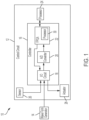
- FIG. 1 illustrates a calibration system 10, in accordance with at least one aspect of the present disclosure.
- the calibration system 10 will be described in the context of its use to calibrate a control circuit 12 of a nuclear power plant. However, it will be appreciated that the calibration system 10 can be utilized to calibrate any number of different devices (an FPGA, a computer, a programmable logic controller, an input/output circuit, etc.), circuits and/or systems.
- the calibration system 10 includes a waveform generator 14 and a controller 16.
- the controller 16 includes an input/output circuit 18, an analog-to-digital (A/D) converter 20 and an FPGA 22.
- the calibration system 10 may also include a processor 24 connected to the FPGA 22.
- the waveform generator 14 is configured to generate one or more waveforms.
- the waveform generator 14 may be configured to generate one or more waveforms such as triangular waves, sine waves, square waves, sawtooth waves, etc. of different amplitudes over a wide range of frequencies.
- An exemplary triangular wave generated by the waveform generator 14 is shown in FIG. 2 , where the triangular wave is a 1 Hx, 0-10 V triangular wave.
- An exemplary sine wave generated by the waveform generator 14 is shown in FIG. 3 . where the sine wave is a 0.5 Hz, 0-10 V sine wave.
- the waveform generator 14 is connected to (in signal communication with) the control circuit 12. More specifically, the waveform generator 14 is connected to (in signal communication with) the input/output circuit 18 of the controller 16.
- the input/output circuit 18 is configured to receive analog signals at its input terminals (not shown for purposes of clarity).
- the input/output circuit 18 may receive analog signals from a sensor 26.
- a sensor 26 Although only one sensor 26 is shown in FIG. 1 , it will be appreciated that the input/output circuit 18 may receive analog signals from a plurality of sensors 26 such as, for example, flow sensors, position sensors, pressure sensors, temperature sensors, etc.
- the input/output circuit 18 may include any number of input/output cards (analog I/O cards, digital I/O cards and/or mixed I/O cards) and may be configured to accommodate both analog and digital inputs/outputs.
- the input/output circuit 18 is further configured to output a control signal to an actuator 28.
- an actuator 28 is shown in FIG. 1 , it will be appreciated that the input/output circuit 18 may output control signals to a plurality of actuators 28 to control a valve, a motor, a pump, etc.
- the A/D converter 20 is connected to (in signal communication with) the input/output circuit 18, and is configured to convert the analog signals received from the input/output circuit 18 into corresponding digital signals or digital values which are representative of the analog signals. Although only one A/D converter 20 is shown in FIG. 1 for purposes of clarity, it will be appreciated that the controller 16 may include any number of A/D converters 20. For example, according to various aspects, the controller 16 includes a separate A/D converter 20 for each analog input/output card in the input/output circuit 18. According to various aspects, the A/D converter 20 forms a part of the input/output circuit 18.
- the FPGA 22 is connected to (in signal communication with) the A/D converter 20, and is configured to process the digital signals and/or digital values received from the A/D converter 20.
- the A/D converter 20 forms a part of the FPGA 22.
- the FPGA 22 may also be utilized for control, filtering, timing and/or other logic functions.
- the FPGA 22 also includes a processor 30 which is in signal communication with the FPGA 22.
- the processor 30 may be utilized for communication, signal processing and/or executing algorithms or routines which are stored in a memory associated with the processor 30.
- the processor 30 can execute one or more such algorithms or routines to implement and control the functionality of the FPGA 22.
- the processor 30 interprets the digital signals or digital values output by the A/D converter 20 and responsively causes the FPGA 22 to output one or more digital signals.
- Such signals may be control signals to control one or more components of the control circuit 12 and/or informational signals to provide information such as a characteristic sensed by an analog sensor 26.
- the FPGA 22, or the combination of the FPGA 22 and the processor 30, may be considered a processing circuit.
- the processor 24 can be in signal communication with the processor 30, and may be utilized, for example, to format information provided by the processor 30 (e.g., information associated with an analog sensor 26 connected to the input/output circuit 18) so that the information can be displayed on a monitor (not shown) connected to the processor 24.
- format information provided by the processor 30 e.g., information associated with an analog sensor 26 connected to the input/output circuit 18
- monitor not shown
- the calibration of the control circuit can be verified by a calibration algorithm or routine executed by the processor 30 of the FPGA 22.
- the processor 30 can verify the timing and voltage levels of the control circuit 12 based on a waveform generated by the waveform generator 14. For example, the sampling rate of the analog signals received by the input/output circuit 18 can be utilized to verify the timing of the control circuit 12 and the voltage levels of the analog signals received by the input/output circuit 18 can be utilized to verify the voltage levels of the control circuit 12. If the calibrations of either the timing or the analog voltages are not verified, the calibrations can be adjusted so that the control circuit 12 is in proper calibration going forward. For example, with respect to the timing of the control circuit 12, loop times utilized by the FPGA 22 can be adjusted to bring the timing into proper calibration. According to other aspects, the calibration or routine can be executed by a processing circuit other than the FPGA 22 and the processor 30.
- a periodic waveform generated by the waveform generator 14 is input to the input/output circuit 18.
- the waveform may be input to a test terminal block (not shown) of the input/output circuit 18.
- the processor 30 initiates the execution of the calibration algorithm or routine.
- the calibration algorithm or routine may be initiated automatically, such as in response to receiving the periodic waveform at a particular input of the input/output circuit 18 (e.g. a test terminal block), or manually in response to an input or command from a user or device.
- Information indicating the type of periodic waveform, the frequency of the periodic waveform and various voltage test points on the periodic waveform may be stored in a memory accessible by the processor 30. According to various aspects, information indicating threshold tolerances for the timing and for each of the voltage test points may also be stored in the memory accessible by the processor 30. The information may be stored in the memory when the FPGA 22 is programmed, such as at time of manufacture. However, it will be appreciated that the FPGA 22 programming can be subsequently updated.
- the processor 30 is configured to verify that the timing of the control circuit 12 is within a predetermined threshold tolerance.
- the analog signal of the periodic waveform is sampled, and the sampled analog values are converted to digital signals or digital values by the A/D converter 20.
- the digital signals or digital values are provided to the FPGA 22 and in turn to the processor 30.
- the processor 30 utilizes the digital signals or digital values to determine the frequency of the periodic waveform.
- the processor 30 can then compare the determined frequency of the periodic waveform with the known frequency of the periodic waveform stored in the memory. If the determined frequency is within the predetermined threshold tolerance of the known frequency, the timing calibration of the control circuit 12 is considered to be verified. For example, if the periodic waveform has a known frequency of 1 Hz and the predetermined threshold tolerance is 1 %, the timing calibration of the control circuit 12 will be considered to be verified if the determined frequency is within 1% of the known frequency of 1 Hz.
- the FPGA 22 (or the processor 30 of the FPGA 22) can be utilized to adjust the calibration of the timing (e.g., by adjusting loop times utilized by the FPGA 22) to bring the timing into proper calibration (i.e., within the predetermined threshold tolerance).
- the processor 30 is also configured to verify that each of the sampled voltage levels along the periodic waveform is within a predetermined threshold tolerance. Once the timing of the control circuit 12 has been verified or brought into proper calibration, the processor 30 can utilize the verified timing to verify each of the sampled voltage levels along the periodic waveform is within the predetermined threshold tolerance. For example, voltage levels associated with a 0-10V periodic waveform such as the triangular wave of FIG. 2 include 0V, 2.5V, 5V, 7.5V, and 10V. Because the timing of the control circuit 12 and the frequency of the periodic waveform are known, the calibration algorithm or routine knows when these voltage levels should occur in the periodic waveform. For the 1Hz, 0-10V triangular wave of FIG.
- the amplitude of the periodic waveform should be 5V at 0.25s and at 0.75s after the start of a period of the waveform, as is shown for example in FIG. 2 . Since the timing has been verified or brought into proper calibration as described above, the processor 30 can utilize the digital signals or digital values corresponding to each of the sampled voltage levels at specific times to compare the sampled voltage values with the expected voltage values. If the sampled voltage values are each within the predetermined threshold tolerance of the expected voltage values, the voltage value calibration of the control circuit 12 is considered to be verified.
- the FPGA 22 (or the processor 30 of the FPGA 22) can be utilized to adjust the calibration of the voltage values (e.g., by adjusting the amplitude of analog signals at the input/output circuit 18) to bring the voltage values into proper calibration (i.e., within the predetermined threshold tolerance).
- the predetermined threshold tolerance e.g., 0.25%, 0.5%, 1%, etc.
- a given predetermined threshold tolerance will be set on a case-by-case basis.
- the timing and voltage levels it utilizes to make control decisions are accurate to the extent they are within the predetermined threshold tolerances of the known/expected timing and voltage levels. If the predetermined threshold tolerance for a given application is 1% and the control circuit 12 interprets an actual 2.5V analog signal as being a 2.8Y analog signal, the control circuit 12 is not properly calibrated and a control operation based on the interpreted voltage level could be unintended, improper and/or unsafe. For these and other reasons, verifying proper calibration and/or adjusting calibration have calibration become part of ongoing maintenance in nuclear plants or other applications. By utilizing the calibration algorithm or routine as described above, the time taken to verify and/or adjust the calibrations are significantly reduced.
- control circuit 12 can use as little as one period of a periodic waveform received from the waveform generator 14 to calibrate itself or verify its own calibration, greatly increasing the speed of the calibration process.
- a facility such as a nuclear plant may include numerous control circuits 12 that need calibrated, increasing the speed of calibration significantly reduces maintenance time.
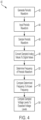
- FIG. 4 illustrates a method 40 of calibrating a control circuit, in accordance with at least one aspect of the present disclosure.
- the method 40 is described in the context of calibrating the control circuit 12, it will be appreciated that the method 40 may be utilized to calibrate any number of different devices (an FPGA, a computer, a programmable logic controller, an input/output circuit, etc.), circuits and/or systems.
- the method 40 may be implemented using the calibration system 10 or other similar systems. For purposes of simplicity, the implementation of the method 40 will be described in the context of the control circuit 12.
- a periodic waveform is generated 42 by, for example, the waveform generator 14.
- the periodic waveform is input 44 to an analog input of the input/output circuit 18.
- the analog signal of the periodic waveform is sampled 46 by the FPGA 22, and the sampled analog values are converted 48 to digital signals or digital values by the A/D converter 20.
- the digital signals or digital values are utilized by the processor 30 to determine 50 the frequency of the periodic waveform.
- the processor 30 compares 52 the determined frequency to the known frequency of the periodic waveform. If the determined frequency is within a predetermined threshold tolerance of the known frequency, the timing of the control circuit 12 is considered to be properly calibrated. If the determined frequency is not within the predetermined threshold tolerance of the known frequency, the timing of the control circuit 12 is adjusted to bring the timing into proper calibration.
- the digital signals or digital values corresponding to the various sampled voltage levels along the periodic waveform and the known frequency of the periodic waveform are utilized by the processor 30 to compare 54 each of the sampled voltage levels along the periodic waveform with the expected voltage levels (the calibration algorithm or routine knows when the expected voltage levels should occur in the periodic waveform). If each of the various sampled voltage levels is within a predetermined threshold tolerance of the expected voltage levels, the voltage levels of the control circuit 12 are considered to be properly calibrated. If each of the various sampled voltage levels is not within a predetermined threshold tolerance of the expected voltage levels, the voltage levels of the control circuit 12 are adjusted to bring the voltage levels into proper calibration. The plurality of voltage levels can be compared to the expected voltage levels sequentially or in parallel.
- the above-described method 40 may be repeated periodically or continuously, and may be repeated any number of times.
Landscapes
- Physics & Mathematics (AREA)
- General Physics & Mathematics (AREA)
- Engineering & Computer Science (AREA)
- General Engineering & Computer Science (AREA)
- Power Engineering (AREA)
- Automation & Control Theory (AREA)
- Analogue/Digital Conversion (AREA)
- Programmable Controllers (AREA)
- Testing Or Calibration Of Command Recording Devices (AREA)
- Tests Of Electronic Circuits (AREA)
- Testing And Monitoring For Control Systems (AREA)
Priority Applications (1)
| Application Number | Priority Date | Filing Date | Title |
|---|---|---|---|
| SI202030555T SI3966585T1 (sl) | 2019-05-10 | 2020-05-07 | Sistem in metoda za umerjanje |
Applications Claiming Priority (2)
| Application Number | Priority Date | Filing Date | Title |
|---|---|---|---|
| US201962845980P | 2019-05-10 | 2019-05-10 | |
| PCT/US2020/031758 WO2020231717A1 (en) | 2019-05-10 | 2020-05-07 | Calibration system and method |
Publications (2)
| Publication Number | Publication Date |
|---|---|
| EP3966585A1 EP3966585A1 (en) | 2022-03-16 |
| EP3966585B1 true EP3966585B1 (en) | 2024-10-02 |
Family
ID=70779982
Family Applications (1)
| Application Number | Title | Priority Date | Filing Date |
|---|---|---|---|
| EP20727551.2A Active EP3966585B1 (en) | 2019-05-10 | 2020-05-07 | Calibration system and method |
Country Status (14)
| Country | Link |
|---|---|
| US (1) | US12013435B2 (enExample) |
| EP (1) | EP3966585B1 (enExample) |
| JP (1) | JP7661239B2 (enExample) |
| KR (1) | KR102870209B1 (enExample) |
| CN (1) | CN114008550B (enExample) |
| BR (1) | BR112021022496A2 (enExample) |
| CA (1) | CA3139887A1 (enExample) |
| ES (1) | ES3006258T3 (enExample) |
| FI (1) | FI3966585T3 (enExample) |
| PL (1) | PL3966585T4 (enExample) |
| SI (1) | SI3966585T1 (enExample) |
| TW (1) | TWI755728B (enExample) |
| UA (1) | UA129058C2 (enExample) |
| WO (1) | WO2020231717A1 (enExample) |
Families Citing this family (2)
| Publication number | Priority date | Publication date | Assignee | Title |
|---|---|---|---|---|
| ES3006258T3 (en) | 2019-05-10 | 2025-03-18 | Westinghouse Electric Co Llc | Calibration system and method |
| TWI832409B (zh) * | 2022-09-02 | 2024-02-11 | 廣達電腦股份有限公司 | 用於校正電池相對電荷狀態的電子裝置及其方法 |
Family Cites Families (29)
| Publication number | Priority date | Publication date | Assignee | Title |
|---|---|---|---|---|
| US4581585A (en) * | 1983-02-07 | 1986-04-08 | Tektronix, Inc. | Apparatus and method for automatically calibrating a sweep waveform generator |
| JPH0310419A (ja) * | 1989-06-07 | 1991-01-18 | Fujitsu Ltd | 周波数特性補正方式 |
| US5412481A (en) * | 1992-02-24 | 1995-05-02 | Samsung Electronics Co., Ltd. | Time-base correction in a video recording/playback system |
| US6988232B2 (en) * | 2001-07-05 | 2006-01-17 | Intellitech Corporation | Method and apparatus for optimized parallel testing and access of electronic circuits |
| US7148828B2 (en) * | 2005-05-03 | 2006-12-12 | Agilent Technologies, Inc. | System and method for timing calibration of time-interleaved data converters |
| US7348914B1 (en) * | 2006-06-29 | 2008-03-25 | Lattice Semiconductor Corporation | Method and systems to align outputs signals of an analog-to-digital converter |
| CN101484819B (zh) * | 2006-06-30 | 2012-05-09 | 泰瑞达公司 | 自动测试装置及与其配套使用的校准设备和校准方法 |
| US7933942B2 (en) * | 2006-09-29 | 2011-04-26 | Teradyne, Inc. | Low cost, high purity sign wave generator |
| JP2008295016A (ja) * | 2007-04-25 | 2008-12-04 | Yokogawa Electric Corp | Ad変換器の校正システム |
| EP2081285A2 (en) * | 2008-01-18 | 2009-07-22 | Power Integrations, Inc. | Cascaded PFC and resonant mode power converters |
| US8102289B2 (en) * | 2009-02-19 | 2012-01-24 | Hitachi, Ltd. | Analog/digital converter and semiconductor integrated circuit device |
| TWI409683B (zh) * | 2010-02-04 | 2013-09-21 | Chunghwa Picture Tubes Ltd | 觸控面板偵測電路 |
| US20110268239A1 (en) * | 2010-04-30 | 2011-11-03 | David Jerome Krieg | Method of calibrating excore detectors in a nuclear reactor |
| JP5785611B2 (ja) * | 2010-05-17 | 2015-09-30 | コーニンクレッカ フィリップス エヌ ヴェ | 不適当な調光器動作を検出し修正するための方法及び装置 |
| US8437974B2 (en) * | 2010-10-08 | 2013-05-07 | Westinghouse Electric Company Llc | Calibration detection system and method |
| US9014813B2 (en) * | 2010-11-03 | 2015-04-21 | Cleveland Clinic Foundation | Apparatus for energy efficient stimulation |
| US8756029B2 (en) | 2011-01-21 | 2014-06-17 | Schneider Electric USA, Inc. | Non-linearity calibration using an internal source in an intelligent electronic device |
| DE102013220157B4 (de) | 2012-10-05 | 2017-05-24 | Infineon Technologies Ag | Signalerzeugungsschaltung |
| US20150341158A1 (en) | 2014-05-23 | 2015-11-26 | Mediatek Inc. | Loop gain calibration apparatus for controlling loop gain of timing recovery loop and related loop gain calibration method |
| US9413344B2 (en) | 2014-09-08 | 2016-08-09 | Qualcomm Incorporated | Automatic calibration circuits for operational calibration of critical-path time delays in adaptive clock distribution systems, and related methods and systems |
| US9270291B1 (en) * | 2015-01-13 | 2016-02-23 | Broadcom Corporation | High speed time-interleaved ADC gain offset and skew mitigation |
| CN104808056B (zh) * | 2015-04-19 | 2018-12-11 | 华南理工大学 | 一种基于比较器转换的频率特性测试方法与装置 |
| CN106300576B (zh) * | 2015-05-11 | 2021-04-20 | 恩智浦美国有限公司 | 用于无线充电系统的双向通信解调方法 |
| US10345418B2 (en) * | 2015-11-20 | 2019-07-09 | Teradyne, Inc. | Calibration device for automatic test equipment |
| US10056914B2 (en) * | 2015-12-18 | 2018-08-21 | Analog Devices Global | Frequency-domain ADC flash calibration |
| US9667407B1 (en) | 2016-05-13 | 2017-05-30 | Credo Technology Group Limited | Integrated multi-channel receiver having independent clock recovery modules with enhanced inductors |
| US10502807B2 (en) | 2017-09-05 | 2019-12-10 | Fluke Corporation | Calibration system for voltage measurement devices |
| CN107861089A (zh) * | 2017-09-26 | 2018-03-30 | 国网江西省电力公司电力科学研究院 | 一种适应于特殊运行工况的智能电能表测试方法 |
| ES3006258T3 (en) | 2019-05-10 | 2025-03-18 | Westinghouse Electric Co Llc | Calibration system and method |
-
2020
- 2020-05-07 ES ES20727551T patent/ES3006258T3/es active Active
- 2020-05-07 BR BR112021022496A patent/BR112021022496A2/pt not_active Application Discontinuation
- 2020-05-07 CN CN202080042778.2A patent/CN114008550B/zh active Active
- 2020-05-07 PL PL20727551.2T patent/PL3966585T4/pl unknown
- 2020-05-07 UA UAA202107061A patent/UA129058C2/uk unknown
- 2020-05-07 SI SI202030555T patent/SI3966585T1/sl unknown
- 2020-05-07 EP EP20727551.2A patent/EP3966585B1/en active Active
- 2020-05-07 JP JP2021566599A patent/JP7661239B2/ja active Active
- 2020-05-07 CA CA3139887A patent/CA3139887A1/en active Pending
- 2020-05-07 FI FIEP20727551.2T patent/FI3966585T3/fi active
- 2020-05-07 KR KR1020217040068A patent/KR102870209B1/ko active Active
- 2020-05-07 WO PCT/US2020/031758 patent/WO2020231717A1/en not_active Ceased
- 2020-05-07 US US17/595,118 patent/US12013435B2/en active Active
- 2020-05-08 TW TW109115447A patent/TWI755728B/zh active
Also Published As
| Publication number | Publication date |
|---|---|
| FI3966585T3 (fi) | 2025-01-03 |
| BR112021022496A2 (pt) | 2022-01-11 |
| WO2020231717A1 (en) | 2020-11-19 |
| TWI755728B (zh) | 2022-02-21 |
| SI3966585T1 (sl) | 2025-04-30 |
| US20220229111A1 (en) | 2022-07-21 |
| PL3966585T3 (pl) | 2025-06-09 |
| JP2022533576A (ja) | 2022-07-25 |
| CA3139887A1 (en) | 2020-11-19 |
| PL3966585T4 (pl) | 2026-03-02 |
| KR20220007639A (ko) | 2022-01-18 |
| ES3006258T3 (en) | 2025-03-18 |
| JP7661239B2 (ja) | 2025-04-14 |
| KR102870209B1 (ko) | 2025-10-14 |
| UA129058C2 (uk) | 2025-01-01 |
| CN114008550B (zh) | 2025-03-14 |
| US12013435B2 (en) | 2024-06-18 |
| CN114008550A (zh) | 2022-02-01 |
| EP3966585A1 (en) | 2022-03-16 |
| TW202111347A (zh) | 2021-03-16 |
Similar Documents
| Publication | Publication Date | Title |
|---|---|---|
| EP3966585B1 (en) | Calibration system and method | |
| US10591585B2 (en) | Electronic control unit for radar sensors | |
| US6653963B1 (en) | Method and apparatus for the A/D conversion of analog signals and corresponding A/D converter arrangement | |
| US9310412B2 (en) | Field device with self-testing of a piezoelectric transducer | |
| US10309804B2 (en) | Encoder signal processor having automatic adjustment function | |
| CN103069711A (zh) | 具有电压谐波整形的电机控制 | |
| US20120086474A1 (en) | Field Device for Process Automation | |
| US20230297814A1 (en) | Method and Device for Calibrating and Operating a Sensor Component with the Aid of Machine Learning Methods | |
| JP2019124596A (ja) | 測定値予測モジュール、測定値予測プログラム及び測定値予測方法 | |
| US20230349954A1 (en) | Current measurement apparatus for measurement value acquisition, current sensor, and current measurement transducer | |
| US8049650B2 (en) | Method for testing a high-speed digital to analog converter based on an undersampling technique | |
| CN111201450B (zh) | 可自测试的测量系统和用于运行可自测试测量系统的方法 | |
| RU2814611C2 (ru) | Способ и система калибровки | |
| EP3349074B1 (en) | Control device, control method, and control program for tuning an amount of operation of a device | |
| RU106768U1 (ru) | Блок управления нагревателями | |
| CN110174607A (zh) | 二进制信号发生器 | |
| Antonyuk et al. | Control Device for Low-Active Parameters in Adaptive Systems with Time Division of Channels | |
| CN109883701A (zh) | 自测试电路和检查信号通过信号路径的完整性的方法 | |
| US6640264B1 (en) | Incremental state logic methodology and apparatus for logic based program control | |
| Pawliczek | Modernization of the fatigue test stand control system using the idea of a virtual instrument | |
| Czaja | A method of self-testing of an analog circuit terminated by an ADC in electronic embedded systems controlled by microcontrollers | |
| EP3754921A1 (en) | Pwm signaling and encoding multiple statuses | |
| EP3759556B1 (en) | Output module, control system and method for testing an output module connected to a complex load | |
| US20160102980A1 (en) | Sensor Element and Method for Capturing a First and a Second Component of a Physical Variable | |
| CN106788801A (zh) | 一种信号校准方法及电子设备 |
Legal Events
| Date | Code | Title | Description |
|---|---|---|---|
| STAA | Information on the status of an ep patent application or granted ep patent |
Free format text: STATUS: UNKNOWN |
|
| STAA | Information on the status of an ep patent application or granted ep patent |
Free format text: STATUS: THE INTERNATIONAL PUBLICATION HAS BEEN MADE |
|
| PUAI | Public reference made under article 153(3) epc to a published international application that has entered the european phase |
Free format text: ORIGINAL CODE: 0009012 |
|
| STAA | Information on the status of an ep patent application or granted ep patent |
Free format text: STATUS: REQUEST FOR EXAMINATION WAS MADE |
|
| 17P | Request for examination filed |
Effective date: 20211110 |
|
| AK | Designated contracting states |
Kind code of ref document: A1 Designated state(s): AL AT BE BG CH CY CZ DE DK EE ES FI FR GB GR HR HU IE IS IT LI LT LU LV MC MK MT NL NO PL PT RO RS SE SI SK SM TR |
|
| DAV | Request for validation of the european patent (deleted) | ||
| DAX | Request for extension of the european patent (deleted) | ||
| GRAP | Despatch of communication of intention to grant a patent |
Free format text: ORIGINAL CODE: EPIDOSNIGR1 |
|
| STAA | Information on the status of an ep patent application or granted ep patent |
Free format text: STATUS: GRANT OF PATENT IS INTENDED |
|
| INTG | Intention to grant announced |
Effective date: 20240425 |
|
| GRAS | Grant fee paid |
Free format text: ORIGINAL CODE: EPIDOSNIGR3 |
|
| GRAA | (expected) grant |
Free format text: ORIGINAL CODE: 0009210 |
|
| STAA | Information on the status of an ep patent application or granted ep patent |
Free format text: STATUS: THE PATENT HAS BEEN GRANTED |
|
| AK | Designated contracting states |
Kind code of ref document: B1 Designated state(s): AL AT BE BG CH CY CZ DE DK EE ES FI FR GB GR HR HU IE IS IT LI LT LU LV MC MK MT NL NO PL PT RO RS SE SI SK SM TR |
|
| REG | Reference to a national code |
Ref country code: GB Ref legal event code: FG4D |
|
| REG | Reference to a national code |
Ref country code: CH Ref legal event code: EP |
|
| REG | Reference to a national code |
Ref country code: DE Ref legal event code: R096 Ref document number: 602020038676 Country of ref document: DE |
|
| REG | Reference to a national code |
Ref country code: IE Ref legal event code: FG4D |
|
| REG | Reference to a national code |
Ref country code: FI Ref legal event code: FGE |
|
| REG | Reference to a national code |
Ref country code: LT Ref legal event code: MG9D |
|
| REG | Reference to a national code |
Ref country code: SE Ref legal event code: TRGR |
|
| REG | Reference to a national code |
Ref country code: NL Ref legal event code: MP Effective date: 20241002 |
|
| REG | Reference to a national code |
Ref country code: AT Ref legal event code: MK05 Ref document number: 1728876 Country of ref document: AT Kind code of ref document: T Effective date: 20241002 |
|
| PG25 | Lapsed in a contracting state [announced via postgrant information from national office to epo] |
Ref country code: NL Free format text: LAPSE BECAUSE OF FAILURE TO SUBMIT A TRANSLATION OF THE DESCRIPTION OR TO PAY THE FEE WITHIN THE PRESCRIBED TIME-LIMIT Effective date: 20241002 |
|
| REG | Reference to a national code |
Ref country code: ES Ref legal event code: FG2A Ref document number: 3006258 Country of ref document: ES Kind code of ref document: T3 Effective date: 20250318 |
|
| PG25 | Lapsed in a contracting state [announced via postgrant information from national office to epo] |
Ref country code: NL Free format text: LAPSE BECAUSE OF FAILURE TO SUBMIT A TRANSLATION OF THE DESCRIPTION OR TO PAY THE FEE WITHIN THE PRESCRIBED TIME-LIMIT Effective date: 20241002 |
|
| PG25 | Lapsed in a contracting state [announced via postgrant information from national office to epo] |
Ref country code: IS Free format text: LAPSE BECAUSE OF FAILURE TO SUBMIT A TRANSLATION OF THE DESCRIPTION OR TO PAY THE FEE WITHIN THE PRESCRIBED TIME-LIMIT Effective date: 20250202 Ref country code: PT Free format text: LAPSE BECAUSE OF FAILURE TO SUBMIT A TRANSLATION OF THE DESCRIPTION OR TO PAY THE FEE WITHIN THE PRESCRIBED TIME-LIMIT Effective date: 20250203 Ref country code: HR Free format text: LAPSE BECAUSE OF FAILURE TO SUBMIT A TRANSLATION OF THE DESCRIPTION OR TO PAY THE FEE WITHIN THE PRESCRIBED TIME-LIMIT Effective date: 20241002 |
|
| PG25 | Lapsed in a contracting state [announced via postgrant information from national office to epo] |
Ref country code: BG Free format text: LAPSE BECAUSE OF FAILURE TO SUBMIT A TRANSLATION OF THE DESCRIPTION OR TO PAY THE FEE WITHIN THE PRESCRIBED TIME-LIMIT Effective date: 20241002 |
|
| PG25 | Lapsed in a contracting state [announced via postgrant information from national office to epo] |
Ref country code: NO Free format text: LAPSE BECAUSE OF FAILURE TO SUBMIT A TRANSLATION OF THE DESCRIPTION OR TO PAY THE FEE WITHIN THE PRESCRIBED TIME-LIMIT Effective date: 20250102 |
|
| PG25 | Lapsed in a contracting state [announced via postgrant information from national office to epo] |
Ref country code: GR Free format text: LAPSE BECAUSE OF FAILURE TO SUBMIT A TRANSLATION OF THE DESCRIPTION OR TO PAY THE FEE WITHIN THE PRESCRIBED TIME-LIMIT Effective date: 20250103 Ref country code: LV Free format text: LAPSE BECAUSE OF FAILURE TO SUBMIT A TRANSLATION OF THE DESCRIPTION OR TO PAY THE FEE WITHIN THE PRESCRIBED TIME-LIMIT Effective date: 20241002 Ref country code: AT Free format text: LAPSE BECAUSE OF FAILURE TO SUBMIT A TRANSLATION OF THE DESCRIPTION OR TO PAY THE FEE WITHIN THE PRESCRIBED TIME-LIMIT Effective date: 20241002 |
|
| PG25 | Lapsed in a contracting state [announced via postgrant information from national office to epo] |
Ref country code: RS Free format text: LAPSE BECAUSE OF FAILURE TO SUBMIT A TRANSLATION OF THE DESCRIPTION OR TO PAY THE FEE WITHIN THE PRESCRIBED TIME-LIMIT Effective date: 20250102 |
|
| PG25 | Lapsed in a contracting state [announced via postgrant information from national office to epo] |
Ref country code: SM Free format text: LAPSE BECAUSE OF FAILURE TO SUBMIT A TRANSLATION OF THE DESCRIPTION OR TO PAY THE FEE WITHIN THE PRESCRIBED TIME-LIMIT Effective date: 20241002 |
|
| REG | Reference to a national code |
Ref country code: DE Ref legal event code: R097 Ref document number: 602020038676 Country of ref document: DE |
|
| PGFP | Annual fee paid to national office [announced via postgrant information from national office to epo] |
Ref country code: FI Payment date: 20250529 Year of fee payment: 6 |
|
| PGFP | Annual fee paid to national office [announced via postgrant information from national office to epo] |
Ref country code: PL Payment date: 20250501 Year of fee payment: 6 |
|
| PG25 | Lapsed in a contracting state [announced via postgrant information from national office to epo] |
Ref country code: DK Free format text: LAPSE BECAUSE OF FAILURE TO SUBMIT A TRANSLATION OF THE DESCRIPTION OR TO PAY THE FEE WITHIN THE PRESCRIBED TIME-LIMIT Effective date: 20241002 |
|
| PGFP | Annual fee paid to national office [announced via postgrant information from national office to epo] |
Ref country code: GB Payment date: 20250523 Year of fee payment: 6 Ref country code: ES Payment date: 20250611 Year of fee payment: 6 |
|
| PGFP | Annual fee paid to national office [announced via postgrant information from national office to epo] |
Ref country code: BE Payment date: 20250527 Year of fee payment: 6 |
|
| PG25 | Lapsed in a contracting state [announced via postgrant information from national office to epo] |
Ref country code: EE Free format text: LAPSE BECAUSE OF FAILURE TO SUBMIT A TRANSLATION OF THE DESCRIPTION OR TO PAY THE FEE WITHIN THE PRESCRIBED TIME-LIMIT Effective date: 20241002 |
|
| PGFP | Annual fee paid to national office [announced via postgrant information from national office to epo] |
Ref country code: FR Payment date: 20250526 Year of fee payment: 6 |
|
| PGFP | Annual fee paid to national office [announced via postgrant information from national office to epo] |
Ref country code: CH Payment date: 20250601 Year of fee payment: 6 |
|
| PG25 | Lapsed in a contracting state [announced via postgrant information from national office to epo] |
Ref country code: RO Free format text: LAPSE BECAUSE OF FAILURE TO SUBMIT A TRANSLATION OF THE DESCRIPTION OR TO PAY THE FEE WITHIN THE PRESCRIBED TIME-LIMIT Effective date: 20241002 |
|
| PG25 | Lapsed in a contracting state [announced via postgrant information from national office to epo] |
Ref country code: SK Free format text: LAPSE BECAUSE OF FAILURE TO SUBMIT A TRANSLATION OF THE DESCRIPTION OR TO PAY THE FEE WITHIN THE PRESCRIBED TIME-LIMIT Effective date: 20241002 |
|
| PGFP | Annual fee paid to national office [announced via postgrant information from national office to epo] |
Ref country code: CZ Payment date: 20250430 Year of fee payment: 6 |
|
| PG25 | Lapsed in a contracting state [announced via postgrant information from national office to epo] |
Ref country code: IT Free format text: LAPSE BECAUSE OF FAILURE TO SUBMIT A TRANSLATION OF THE DESCRIPTION OR TO PAY THE FEE WITHIN THE PRESCRIBED TIME-LIMIT Effective date: 20241002 |
|
| PGFP | Annual fee paid to national office [announced via postgrant information from national office to epo] |
Ref country code: SE Payment date: 20250529 Year of fee payment: 6 Ref country code: SI Payment date: 20250508 Year of fee payment: 6 |
|
| PLBE | No opposition filed within time limit |
Free format text: ORIGINAL CODE: 0009261 |
|
| STAA | Information on the status of an ep patent application or granted ep patent |
Free format text: STATUS: NO OPPOSITION FILED WITHIN TIME LIMIT |
|
| 26N | No opposition filed |
Effective date: 20250703 |
|
| REG | Reference to a national code |
Ref country code: DE Ref legal event code: R119 Ref document number: 602020038676 Country of ref document: DE |
|
| PG25 | Lapsed in a contracting state [announced via postgrant information from national office to epo] |
Ref country code: LU Free format text: LAPSE BECAUSE OF NON-PAYMENT OF DUE FEES Effective date: 20250507 |
|
| PG25 | Lapsed in a contracting state [announced via postgrant information from national office to epo] |
Ref country code: MC Free format text: LAPSE BECAUSE OF FAILURE TO SUBMIT A TRANSLATION OF THE DESCRIPTION OR TO PAY THE FEE WITHIN THE PRESCRIBED TIME-LIMIT Effective date: 20241002 |
|
| PG25 | Lapsed in a contracting state [announced via postgrant information from national office to epo] |
Ref country code: IE Free format text: LAPSE BECAUSE OF NON-PAYMENT OF DUE FEES Effective date: 20250507 Ref country code: DE Free format text: LAPSE BECAUSE OF NON-PAYMENT OF DUE FEES Effective date: 20251202 |