EP3923346A1 - Verfahren zur herstellung eines trench-mosfet - Google Patents
Verfahren zur herstellung eines trench-mosfet Download PDFInfo
- Publication number
- EP3923346A1 EP3923346A1 EP21173797.8A EP21173797A EP3923346A1 EP 3923346 A1 EP3923346 A1 EP 3923346A1 EP 21173797 A EP21173797 A EP 21173797A EP 3923346 A1 EP3923346 A1 EP 3923346A1
- Authority
- EP
- European Patent Office
- Prior art keywords
- trenches
- layer
- polysilicon
- ion implantation
- implantation
- Prior art date
- Legal status (The legal status is an assumption and is not a legal conclusion. Google has not performed a legal analysis and makes no representation as to the accuracy of the status listed.)
- Pending
Links
Images



Classifications
-
- H—ELECTRICITY
- H10—SEMICONDUCTOR DEVICES; ELECTRIC SOLID-STATE DEVICES NOT OTHERWISE PROVIDED FOR
- H10D—INORGANIC ELECTRIC SEMICONDUCTOR DEVICES
- H10D62/00—Semiconductor bodies, or regions thereof, of devices having potential barriers
- H10D62/80—Semiconductor bodies, or regions thereof, of devices having potential barriers characterised by the materials
- H10D62/83—Semiconductor bodies, or regions thereof, of devices having potential barriers characterised by the materials being Group IV materials, e.g. B-doped Si or undoped Ge
- H10D62/832—Semiconductor bodies, or regions thereof, of devices having potential barriers characterised by the materials being Group IV materials, e.g. B-doped Si or undoped Ge being Group IV materials comprising two or more elements, e.g. SiGe
- H10D62/8325—Silicon carbide
-
- H—ELECTRICITY
- H10—SEMICONDUCTOR DEVICES; ELECTRIC SOLID-STATE DEVICES NOT OTHERWISE PROVIDED FOR
- H10D—INORGANIC ELECTRIC SEMICONDUCTOR DEVICES
- H10D30/00—Field-effect transistors [FET]
- H10D30/01—Manufacture or treatment
- H10D30/021—Manufacture or treatment of FETs having insulated gates [IGFET]
- H10D30/028—Manufacture or treatment of FETs having insulated gates [IGFET] of double-diffused metal oxide semiconductor [DMOS] FETs
- H10D30/0291—Manufacture or treatment of FETs having insulated gates [IGFET] of double-diffused metal oxide semiconductor [DMOS] FETs of vertical DMOS [VDMOS] FETs
- H10D30/0295—Manufacture or treatment of FETs having insulated gates [IGFET] of double-diffused metal oxide semiconductor [DMOS] FETs of vertical DMOS [VDMOS] FETs using recessing of the source electrodes
-
- H—ELECTRICITY
- H10—SEMICONDUCTOR DEVICES; ELECTRIC SOLID-STATE DEVICES NOT OTHERWISE PROVIDED FOR
- H10D—INORGANIC ELECTRIC SEMICONDUCTOR DEVICES
- H10D30/00—Field-effect transistors [FET]
- H10D30/01—Manufacture or treatment
- H10D30/021—Manufacture or treatment of FETs having insulated gates [IGFET]
- H10D30/028—Manufacture or treatment of FETs having insulated gates [IGFET] of double-diffused metal oxide semiconductor [DMOS] FETs
- H10D30/0291—Manufacture or treatment of FETs having insulated gates [IGFET] of double-diffused metal oxide semiconductor [DMOS] FETs of vertical DMOS [VDMOS] FETs
- H10D30/0297—Manufacture or treatment of FETs having insulated gates [IGFET] of double-diffused metal oxide semiconductor [DMOS] FETs of vertical DMOS [VDMOS] FETs using recessing of the gate electrodes, e.g. to form trench gate electrodes
-
- H—ELECTRICITY
- H10—SEMICONDUCTOR DEVICES; ELECTRIC SOLID-STATE DEVICES NOT OTHERWISE PROVIDED FOR
- H10D—INORGANIC ELECTRIC SEMICONDUCTOR DEVICES
- H10D30/00—Field-effect transistors [FET]
- H10D30/60—Insulated-gate field-effect transistors [IGFET]
- H10D30/64—Double-diffused metal-oxide semiconductor [DMOS] FETs
- H10D30/66—Vertical DMOS [VDMOS] FETs
- H10D30/668—Vertical DMOS [VDMOS] FETs having trench gate electrodes, e.g. UMOS transistors
-
- H—ELECTRICITY
- H10—SEMICONDUCTOR DEVICES; ELECTRIC SOLID-STATE DEVICES NOT OTHERWISE PROVIDED FOR
- H10D—INORGANIC ELECTRIC SEMICONDUCTOR DEVICES
- H10D64/00—Electrodes of devices having potential barriers
- H10D64/01—Manufacture or treatment
- H10D64/013—Manufacture or treatment of electrodes having a conductor capacitively coupled to a semiconductor by an insulator
- H10D64/01366—Manufacture or treatment of electrodes having a conductor capacitively coupled to a semiconductor by an insulator the semiconductor being silicon carbide
-
- H—ELECTRICITY
- H10—SEMICONDUCTOR DEVICES; ELECTRIC SOLID-STATE DEVICES NOT OTHERWISE PROVIDED FOR
- H10D—INORGANIC ELECTRIC SEMICONDUCTOR DEVICES
- H10D64/00—Electrodes of devices having potential barriers
- H10D64/20—Electrodes characterised by their shapes, relative sizes or dispositions
- H10D64/27—Electrodes not carrying the current to be rectified, amplified, oscillated or switched, e.g. gates
- H10D64/311—Gate electrodes for field-effect devices
- H10D64/411—Gate electrodes for field-effect devices for FETs
- H10D64/511—Gate electrodes for field-effect devices for FETs for IGFETs
- H10D64/512—Disposition of the gate electrodes, e.g. buried gates
- H10D64/513—Disposition of the gate electrodes, e.g. buried gates within recesses in the substrate, e.g. trench gates, groove gates or buried gates
-
- H—ELECTRICITY
- H10—SEMICONDUCTOR DEVICES; ELECTRIC SOLID-STATE DEVICES NOT OTHERWISE PROVIDED FOR
- H10D—INORGANIC ELECTRIC SEMICONDUCTOR DEVICES
- H10D64/00—Electrodes of devices having potential barriers
- H10D64/20—Electrodes characterised by their shapes, relative sizes or dispositions
- H10D64/23—Electrodes carrying the current to be rectified, amplified, oscillated or switched, e.g. sources, drains, anodes or cathodes
- H10D64/251—Source or drain electrodes for field-effect devices
- H10D64/252—Source or drain electrodes for field-effect devices for vertical or pseudo-vertical devices
- H10D64/2527—Source or drain electrodes for field-effect devices for vertical or pseudo-vertical devices for vertical devices wherein the source or drain electrodes are recessed in semiconductor bodies
-
- H—ELECTRICITY
- H10—SEMICONDUCTOR DEVICES; ELECTRIC SOLID-STATE DEVICES NOT OTHERWISE PROVIDED FOR
- H10D—INORGANIC ELECTRIC SEMICONDUCTOR DEVICES
- H10D64/00—Electrodes of devices having potential barriers
- H10D64/20—Electrodes characterised by their shapes, relative sizes or dispositions
- H10D64/27—Electrodes not carrying the current to be rectified, amplified, oscillated or switched, e.g. gates
- H10D64/311—Gate electrodes for field-effect devices
- H10D64/411—Gate electrodes for field-effect devices for FETs
- H10D64/511—Gate electrodes for field-effect devices for FETs for IGFETs
- H10D64/517—Gate electrodes for field-effect devices for FETs for IGFETs characterised by the conducting layers
- H10D64/518—Gate electrodes for field-effect devices for FETs for IGFETs characterised by the conducting layers characterised by their lengths or sectional shapes
-
- H—ELECTRICITY
- H10—SEMICONDUCTOR DEVICES; ELECTRIC SOLID-STATE DEVICES NOT OTHERWISE PROVIDED FOR
- H10P—GENERIC PROCESSES OR APPARATUS FOR THE MANUFACTURE OR TREATMENT OF DEVICES COVERED BY CLASS H10
- H10P30/00—Ion implantation into wafers, substrates or parts of devices
- H10P30/20—Ion implantation into wafers, substrates or parts of devices into semiconductor materials, e.g. for doping
- H10P30/202—Ion implantation into wafers, substrates or parts of devices into semiconductor materials, e.g. for doping characterised by the semiconductor materials
- H10P30/204—Ion implantation into wafers, substrates or parts of devices into semiconductor materials, e.g. for doping characterised by the semiconductor materials into Group IV semiconductors
- H10P30/2042—Ion implantation into wafers, substrates or parts of devices into semiconductor materials, e.g. for doping characterised by the semiconductor materials into Group IV semiconductors into crystalline silicon carbide
-
- H—ELECTRICITY
- H10—SEMICONDUCTOR DEVICES; ELECTRIC SOLID-STATE DEVICES NOT OTHERWISE PROVIDED FOR
- H10P—GENERIC PROCESSES OR APPARATUS FOR THE MANUFACTURE OR TREATMENT OF DEVICES COVERED BY CLASS H10
- H10P30/00—Ion implantation into wafers, substrates or parts of devices
- H10P30/20—Ion implantation into wafers, substrates or parts of devices into semiconductor materials, e.g. for doping
- H10P30/21—Ion implantation into wafers, substrates or parts of devices into semiconductor materials, e.g. for doping of electrically active species
-
- H—ELECTRICITY
- H10—SEMICONDUCTOR DEVICES; ELECTRIC SOLID-STATE DEVICES NOT OTHERWISE PROVIDED FOR
- H10P—GENERIC PROCESSES OR APPARATUS FOR THE MANUFACTURE OR TREATMENT OF DEVICES COVERED BY CLASS H10
- H10P30/00—Ion implantation into wafers, substrates or parts of devices
- H10P30/20—Ion implantation into wafers, substrates or parts of devices into semiconductor materials, e.g. for doping
- H10P30/222—Ion implantation into wafers, substrates or parts of devices into semiconductor materials, e.g. for doping characterised by the angle between the ion beam and the crystal planes or the main crystal surface
-
- H—ELECTRICITY
- H10—SEMICONDUCTOR DEVICES; ELECTRIC SOLID-STATE DEVICES NOT OTHERWISE PROVIDED FOR
- H10P—GENERIC PROCESSES OR APPARATUS FOR THE MANUFACTURE OR TREATMENT OF DEVICES COVERED BY CLASS H10
- H10P30/00—Ion implantation into wafers, substrates or parts of devices
- H10P30/20—Ion implantation into wafers, substrates or parts of devices into semiconductor materials, e.g. for doping
- H10P30/28—Ion implantation into wafers, substrates or parts of devices into semiconductor materials, e.g. for doping characterised by an annealing step, e.g. for activation of dopants
-
- H—ELECTRICITY
- H10—SEMICONDUCTOR DEVICES; ELECTRIC SOLID-STATE DEVICES NOT OTHERWISE PROVIDED FOR
- H10P—GENERIC PROCESSES OR APPARATUS FOR THE MANUFACTURE OR TREATMENT OF DEVICES COVERED BY CLASS H10
- H10P95/00—Generic processes or apparatus for manufacture or treatments not covered by the other groups of this subclass
- H10P95/90—Thermal treatments, e.g. annealing or sintering
- H10P95/906—Thermal treatments, e.g. annealing or sintering for altering the shape of semiconductors, e.g. smoothing the surface
Definitions
- the present invention relates to a method for producing a trench MOSFET, in which trenches are produced in a monocrystalline semiconductor layer and at least partially filled with polysilicon prior to ion implantation to produce source regions and well regions.
- Trench MOSFETs Metal-Oxide-Semiconductor Field-Effect Transistor
- MOSFETs Metal-Oxide-Semiconductor Field-Effect Transistor
- Trench MOSFETs have the advantage over planar MOSFETs that the JFET region present in planar MOSFETs and the associated electrical resistance are omitted. They therefore have a lower resistance and, due to their greater integration density, allow a saving in chip area and thus also manufacturing costs.
- lithography masks In the manufacture of trench MOSFETs, lithography masks have so far often been used, with which all structures to be transferred into the component are defined by correspondingly transparent and opaque areas. For a mask-compliant structure transfer, lithography masks with a correspondingly high resolution and adjustment capability are required necessary, although here, too, technology-related limitations cannot be undercut. This leads to correspondingly high costs. Self-adjusting manufacturing processes are known to avoid such lithography masks when generating the source regions and the well regions by ion implantation.
- the state of the art for self-aligning manufacturing processes for trench MOSFETs in silicon is the production of self-aligned n + source contacts or p-well regions after the trench structure has been produced, also referred to as "trench first".
- the US 9735266 B2 shows an example of this manufacturing technique.
- the trenches are etched into the monocrystalline silicon layer to a depth of 40 ⁇ m and then a thin oxide is thermally grown.
- a polysilicon layer is then deposited in order to at least partially fill the trenches with polysilicon.
- the polysilicon present between the trenches is removed by dry etching.
- a thin oxide layer is then deposited over the entire surface and removed from the trench walls using a wet etching process (BOE: Buffered Oxide Etch). After the local isotropic etching of the silicon layer down to the surface of the polysilicon, the self- aligning n + source and p-well implantation takes place.
- This technology is suitable for producing trench MOSFETs in silicon, but due to the different material properties it cannot be transferred identically to silicon carbide (SiC).
- n + source and p-well regions are initially implanted over the entire area in the active area of the SiC layer.
- the trenches are then only subsequently etched into these implanted areas.
- the control of the etching process is difficult here, however, since the etching process depends on the doping of the areas.
- the US 2008/0081422 A1 describes a method for producing a trench MOSFET, in which trenches are produced in a monocrystalline semiconductor layer, into which a scattering oxide layer and a polysilicon layer are deposited.
- the polysilicon layer is planarized except for the surfaces of the semiconductor layer between the trenches and a thermal SiO2 layer is produced over the polysilicon in the trenches.
- the SiO2 layer forms an implantation mask for subsequent implantation steps, in which source regions of a first doping type and well regions of a second doping type are generated.
- a similar approach is also used in the US 2010/0032751 A1 disclosed.
- the object of the present invention is to provide a method for producing a trench MOSFET which is suitable for the production of Trench MOSFETs in monocrystalline SiC layers are suitable, do not require lithography masks for generating the source and well regions and enable the production of a uniform trench structure.
- the trenches are first produced in a monocrystalline, in particular epitaxial, semiconductor layer by means of a suitable etching process.
- a scatter oxide layer, preferably over the entire area, and then a polysilicon layer are then deposited so that the trenches are at least partially filled with polysilicon.
- the polysilicon layer is then planarized except for the surfaces of the semiconductor layer between the trenches, preferably by dry etching.
- the method is characterized in that, prior to the implantation steps for generating the source and well regions, in particular n + source and p well, a sufficiently thick SiO 2 layer is placed over the polysilicon by thermal oxidation of the exposed surfaces of the polysilicon the trenches is generated, which serves as an implantation mask for the subsequent implantation steps and prevents the risk of conductive channels on the side walls of the trenches, which could otherwise form as a result of an imperfectly planarized polysilicon surface.
- a sufficiently thick SiO 2 layer is placed over the polysilicon by thermal oxidation of the exposed surfaces of the polysilicon the trenches is generated, which serves as an implantation mask for the subsequent implantation steps and prevents the risk of conductive channels on the side walls of the trenches, which could otherwise form as a result of an imperfectly planarized polysilicon surface.
- a sufficiently thick SiO 2 layer is placed over the polysilicon by thermal oxidation of the exposed surfaces of the polysilicon the trenches is generated, which serves as an
- the thermal oxidation of the polysilicon can be carried out until the level of the surface of the thermal oxide layer reaches the level of the surface of the semiconductor layer between trenches (MESA structure). Often - but not in every case - the thermal oxide layer is produced with a thickness> 100 nm.
- the proposed production method manages without lithography steps for producing the source and well regions of the component and is therefore independent of the resolution and adjustment capability of a lithography system. Due to the reliable implantation masking by means of oxidized polysilicon in the trenches (thermal oxide layer), the continuous source and well areas immediately adjacent to the edge of the trench are implemented in such a way that the risk of a conductive channel forming on the side walls of the trench is eliminated.
- the doping in the channel region of the transistor can also be adjusted by selecting the thermal oxide thickness over the polysilicon. This influences the threshold voltage and the channel length as essential factors of the channel resistance. At the same time, in comparison to a “trench load” process, this procedure does not result in a reduction in the dielectric strength of the Component structures. In the latter case, the dimensioning of the well doping is restricted towards low dopant concentrations.
- a thin scattering oxide layer is deposited over the entire area, since the thin scattering oxide layer initially deposited may be during the Planarization of the polysilicon was removed in some places.
- the polysilicon with the thermal oxide layer lying above it is removed from the trenches. Subsequently, p + regions can be generated via a masking process by ion implantation, which serve as shielding. A gate oxide layer and, in turn, a polysilicon layer are then deposited and planarized in the trenches. As a subsequent step, a suitable metallization is applied to create ohmic contacts for gate, source and drain.
- the proposed method is particularly suitable for the production of trench MOSFETs in monocrystalline, in particular epitaxially grown SiC, but can in principle also be used for the production of such MOSFETs in other semiconductor materials such as Si or GaN.
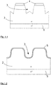
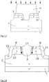
- the proposed method for producing a trench MOSFET in an epitaxial SiC layer is described below with reference to FIG Figures 1.1 - 1.9 explained again by way of example.
- the MOSFET is produced in an epitaxially grown SiC layer 2 with n - doping on an n + substrate 1 made of SiC.
- the trenches 3 are produced in the SiC layer 2.
- a hard mask 4 made of SiO 2 is applied by means of PECVD (PECVD: Plasma Enhanced Chemical Vapor Deposition) with a thickness of 1000 nm in this example.
- PECVD Plasma Enhanced Chemical Vapor Deposition
- the edges of the trenches 3 are smoothed by a high-temperature treatment.
- a thin layer of scattered oxide is then applied over the entire surface 5 deposited (cf. Figure 1.2 ), which is intended to prevent grid guide effects (channeling) in the later implantation steps.
- a planarization layer of sufficient thickness made of polysilicon 6 is then deposited, through which the trenches 3 are at least partially filled. The deposition takes place over the entire area, that is to say also on the MESA structures between the trenches 3.
- the surface is then planarized using a dry etching process, the polysilicon being removed from the MESA structures, as shown in FIG Figure 1.3 can be seen.
- the dry etching process is selective to the oxide layer (scattered oxide 5) located under the polysilicon layer and ends when the oxide surface of the MESA structures is exposed from the polysilicon layer.
- the polysilicon 6 located in the trenches 3 is retained in this case.
- the polysilicon 6 is thermally oxidized in the trenches in order to produce a sufficiently thick thermal SiO 2 layer 7 on the polysilicon 6.
- This is in Figure 1.4 and can take place, for example, by moist oxidation at 950 ° C.
- the relatively low temperature of ⁇ 1000 ° C selected for the moist oxidation has the advantage that silicon carbide is hardly oxidized at this temperature (only a few nm), while polysilicon is much faster or stronger.
- This thermal SiO 2 layer 7 is produced so thick that it forms a reliable implantation masking for the later implantation steps for producing the n + source and p-well regions. This layer reduces the risk of a conductive channel being formed the side walls of the trench eliminated.
- a thin layer of scattering oxide 8 is then deposited over the entire surface in order to replace any scattering oxide that may have been removed by the previous dry etching process.
- the ion implantation for producing the p-well regions 10 takes place in this example with the substrate being tilted by an angle of + 7 ° and -7 °, in order to again avoid possible grid guidance effects (channeling).
- FIG. 1.8 shows the result after performing a tempering step. After the annealing, the p-well regions 10 in the vicinity of the side walls of the trench are curved upwards due to a diffusion effect, as shown in FIG Figure 1.8 can be seen.
- a polysilicon layer 14 is then deposited in a known manner over a previously deposited SiO 2 layer 13, which serves as a gate oxide, and metallization layers are applied to realize the ohmic contacts, as is the case for the source contact 15 and the drain.
- Contact 16 in Figure 1.9 is shown.
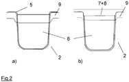
- An essential step in the proposed production method consists in producing the sufficiently thick thermal SiO 2 layer 7 over the polysilicon 6 in the trenches 3, by means of which the risk of conductive channels forming on the side walls of the trenches is eliminated.
- Figure 2 shows the influence of this thermal oxide layer 7 on the course of the doping of the n + source regions 9 on the basis of a KMC (Kinetic Monte Carlo) simulation (shown here in a greatly simplified manner).
- KMC Kinetic Monte Carlo simulation
Landscapes
- Electrodes Of Semiconductors (AREA)
Abstract
Description
- Die vorliegende Erfindung betrifft ein Verfahren zur Herstellung eines Trench-MOSFET, bei dem vor einer Ionenimplantation zur Erzeugung von Source-Gebieten und Wannen-Gebieten Gräben in einer monokristallinen Halbleiterschicht erzeugt und zumindest teilweise mit Polysilizium aufgefüllt werden.
- Trench-MOSFETs (MOSFET: Metal-Oxide-Semiconductor Field-Effect Transistor) sind vertikal aufgebaute Transistorbauelemente, bei denen der Transistorkanal vertikal verläuft. Trench-MOSFETs haben gegenüber planaren MOSFETs den Vorteil, dass die bei planaren MOSFETs vorhandene JFET-Region und der damit verbundene elektrische Widerstand entfallen. Sie weisen daher einen geringeren Widerstand auf und ermöglichen aufgrund ihrer größeren Integrationsdichte eine Einsparung an Chipfläche und damit auch Herstellungskosten.
- Bei der Herstellung von Trench-MOSFETs werden bisher häufig Lithographiemasken eingesetzt, mit denen alle in das Bauelement zu übertragenden Strukturen durch entsprechend lichtdurchlässige und lichtundurchlässige Bereiche definiert sind. Für eine maskenkonforme Strukturübertragung sind Lithographiemasken mit entsprechend hohem Auflösungs- und Justiervermögen notwendig, wobei auch hier technologiebedingte Limitationen nicht unterschritten werden können. Dies führt zu entsprechend hohen Kosten. Zur Vermeidung derartiger Lithographiemasken bei der Erzeugung der Source-Bereiche und der Wannen-Bereiche durch Ionenimplantation sind selbstjustierende Herstellungsprozesse bekannt.
- Der Stand der Technik zu selbstjustierenden Herstellungsprozessen von Trench-MOSFETs in Silizium (Si) ist die Erzeugung von selbstjustierten n+-Sourcekontakten bzw. p-Wanne-Gebieten nach erfolgter Erzeugung der Grabenstruktur, auch als "Trench-First" bezeichnet. Die
US 9735266 B2 - Daher wird für die Herstellung von Trench-MOSFETs in monokristallinen Schichten aus Siliziumcarbid bisher eine andere selbstjustierende Herstellungstechnik eingesetzt, bei der die Erzeugung der Grabenstruktur nach erfolgter Ionenimplantation erfolgt ("Trench-Last"). Ein Beispiel für diese Herstellungstechnik ist in der
US 5614749 A beschrieben. Grundsätzlich werden hierbei die n+-Source und p-Wanne-Gebiete zunächst ganzflächig in den aktiven Bereich der SiC-Schicht implantiert. Die Gräben werden dann erst anschließend in diese implantierten Gebiete geätzt. Die Steuerung des Ätzprozesses ist hierbei jedoch schwierig, da der Ätzprozess von der Dotierung der Bereiche abhängt. - Die
US 2008/0081422 A1 beschreibt ein Verfahren zur Herstellung eines Trench-MOSFET, bei dem in einer monokristallinen Halbleiterschicht Gräben erzeugt werden, in die eine Streuoxid-Schicht und eine Polysiliziumschicht abgeschieden werden. Die Polysiliziumschicht wird bis auf Oberflächen der Halbleiterschicht zwischen den Gräben planarisiert und eine thermische SiO2-Schicht über dem Polysilizium in den Gräben erzeugt. Die SiO2-Schicht bildet eine Implantationsmaske für nachfolgende Implantationsschritte, bei denen Source-Gebiete eines ersten Dotierungstyps und Wannen-Gebiete eines zweiten Dotierungstyps erzeugt werden. Eine ähnliche Vorgehensweise ist auch in derUS 2010/0032751 A1 offenbart. - Die Aufgabe der vorliegenden Erfindung besteht darin, ein Verfahren zur Herstellung eines Trench-MOSFET anzugeben, das sich für die Herstellung von Trench-MOSFETs in monokristallinen SiC-Schichten eignet, ohne Lithographiemasken für die Erzeugung der Source- und Wannen-Gebiete auskommt und die Herstellung einer gleichmäßigen Grabenstruktur ermöglicht.
- Die Aufgabe wird mit dem Verfahren gemäß Patentanspruch 1 gelöst. Vorteilhafte Ausgestaltungen des Verfahrens sind Gegenstand der abhängigen Patentansprüche oder lassen sich der nachfolgenden Beschreibung sowie dem Ausführungsbeispiel entnehmen. Bei dem vorgeschlagenen Verfahren werden zunächst die Gräben in einer monokristallinen, insbesondere epitaktischen, Halbleiterschicht durch einen geeigneten Ätzprozess erzeugt. Anschließend wird eine Streuoxid-Schicht, vorzugsweise ganzflächig, und anschließend eine Polysiliziumschicht abgeschieden, so dass die Gräben zumindest teilweise mit Polysilizium aufgefüllt sind. Die Polysiliziumschicht wird dann bis auf Oberflächen der Halbleiterschicht zwischen den Gräben planarisiert, vorzugsweise durch Trockenätzen. Das Verfahren zeichnet sich dadurch aus, dass vor den Implantationsschritten zur Erzeugung der Source- und Wannen-Bereiche, insbesondere n+-Source und p-Wanne, durch thermische Oxidation der freiliegenden Oberflächen des Polysiliziums eine ausreichend dicke SiO2-Schicht über dem Polysilizium in den Gräben erzeugt wird, die als Implantationsmaske für die nachfolgenden Implantationsschritte dient und die Gefahr leitfähiger Kanäle an den Seitenwänden der Gräben verhindert, die sich ansonsten als Folge einer nicht perfekt planarisierten Polysiliziumoberfläche bilden könnten. Über die Dicke dieser thermischen Oxidschicht kann auch die Dotierung im Transistorkanal und damit die Schwellspannung und die Kanallänge beeinflusst werden. Die Dicke der thermischen Oxidschicht kann über die Oxidationszeit und die Temperatur bei der Oxidation gesteuert werden. Die thermische Oxidation des Polysiliziums kann dabei so lange durchgeführt werden, bis das Niveau der Oberfläche der thermischen Oxidschicht das Niveau der Oberfläche der Halbleiterschicht zwischen Gräben (MESA-Struktur) erreicht. Häufig - aber nicht in jedem Fall - wird die thermische Oxidschicht mit einer Dicke > 100 nm erzeugt.
- Das vorgeschlagene Herstellungsverfahren kommt ohne Lithographieschritte zur Erzeugung der Source- und Wannen-Gebiete des Bauelementes aus und ist somit unabhängig vom Auflösungs- und Justiervermögen einer Lithographieanlage. Durch die zuverlässige Implantationsmaskierung mittels oxidiertem Polysilizium in den Gräben (thermische Oxidschicht) werden die durchgehenden, unmittelbar bis an den Rand des Grabens grenzenden Source- und Wannen-Gebiete so realisiert, dass das Risiko eines sich ausbildenden leitfähigen Kanals an den Grabenseitenwänden eliminiert wird. Bei dem vorgeschlagenen Verfahren lässt sich auch die Dotierung im Kanalbereich des Transistors durch die Wahl der thermischen Oxiddicke über dem Polysilizium einstellen. Dies beeinflusst die Einsatzspannung und die Kanallänge als wesentliche Faktoren des Kanalwiderstands. Gleichzeitig ergibt sich im Vergleich zu einem "Trench-Last"-Prozess bei diesem Vorgehen keine Reduzierung der Spannungsfestigkeit der Bauelementstrukturen. Bei letzterem ist die Dimensionierung der Wannen-Dotierung hin zu niedrigen Dotierstoffkonzentrationen eingeschränkt.
- In einer vorteilhaften Ausgestaltung des vorgeschlagenen Verfahrens erfolgt nach der thermischen Oxidation zur Erzeugung der ausreichend dicken thermischen SiO2- bzw. Oxidschicht über dem Polysilizium in den Gräben eine ganzflächige Abscheidung einer dünnen Streuoxid-Schicht, da die anfänglich abgeschiedene dünne Streuoxid-Schicht möglicherweise bei der Planarisierung des Polysiliziums an manchen Stellen entfernt wurde.
- Nach der Erzeugung der Source- und Wannen-Gebiete des ersten und zweiten Dotierungstyps wird das Polysilizium mit der darüber liegenden thermischen Oxidschicht aus den Gräben entfernt. Anschließend können p+-Gebiete über einen Maskierungsprozess durch Ionenimplantation erzeugt werden, die als Abschirmung dienen. In die Gräben wird dann eine Gate-Oxidschicht und wiederum eine Polysiliziumschicht abgeschieden und planarisiert. Als nachfolgender Schritt wird eine geeignete Metallisierung zur Erstellung ohmscher Kontakte für Gate, Source und Drain aufgebracht.
- Das vorgeschlagene Verfahren eignet sich besonders für die Erzeugung von Trench-MOSFETs in monokristallinem, insbesondere epitaktisch gewachsenem SiC, lässt sich jedoch prinzipiell auch für die Erzeugung derartiger MOSFETs in anderen Halbleitermaterialien wie Si oder GaN einsetzen.
- Das vorgeschlagene Verfahren wird nachfolgend anhand eines Ausführungsbeispiels in Verbindung mit den Zeichnungen nochmals näher erläutert. Hierbei zeigen:
- Fig. 1.1-1.9
- verschiedene Herstellungsschritte zur Herstellung eines Trench-MOSFET gemäß dem vorgeschlagenen Verfahren; und
- Fig. 2
- einen Vergleich der n+-Source-Implantation mit und ohne die thermische Oxidschicht des vorgeschlagenen Verfahrens auf Basis einer TCAD (Technology Computer-Aided Design) Prozess-Simulation.
- Das vorgeschlagene Verfahren wird zur Herstellung eines Trench-MOSFET in einer epitaktischen SiC-Schicht im Folgenden anhand der
Figuren 1.1 - 1.9 nochmals beispielhaft erläutert. Die Herstellung des MOSFET erfolgt hierbei in einer epitaktisch gewachsenen SiC-Schicht 2 mit einer n--Dotierung auf einem n+-Substrat 1 aus SiC. Zunächst werden in der SiC-Schicht 2 die Gräben 3 erzeugt. Hierzu wird eine Hartmaske 4 aus SiO2 mittels PECVD (PECVD: Plasma Enhanced Chemical Vapor Deposition) mit einer Dicke von in diesem Beispiel 1000 nm aufgebracht. Die Gräben 3 werden dann durch Trockenätzen in der SiC-Schicht 2 erzeugt, wie dies inFigur 1.1 angedeutet ist. Durch eine Hochtemperaturbehandlung werden die Kanten der Gräben 3 geglättet. Anschließend wird ganzflächig eine dünne Streuoxid-Schicht 5 abgeschieden (vgl.Figur 1.2 ), das Gitterführungseffekte (Channeling) bei den späteren Implantationsschritten verhindern soll. Danach wird eine Planarisierungsschicht ausreichender Dicke aus Polysilizium 6 abgeschieden, durch die die Gräben 3 zumindest teilweise aufgefüllt werden. Die Abscheidung erfolgt hierbei ganzflächig, also auch auf den MESA-Strukturen zwischen den Gräben 3. Die Oberfläche wird anschließend mit einem Trockenätzprozess planarisiert, wobei das Polysilizium von den MESA-Strukturen entfernt wird, wie dies inFigur 1.3 zu erkennen ist. Der Trockenätzprozess verhält sich selektiv zu der unter der Polysiliziumschicht befindlichen Oxidschicht (Streuoxid 5) und endet, wenn die Oxidoberfläche der MESA-Strukturen von der Polysiliziumschicht freigelegt ist. Das sich in den Gräben 3 befindliche Polysilizium 6 bleibt hierbei erhalten. - Im nächsten Prozessschritt erfolgt eine thermische Oxidation des Polysiliziums 6 in den Gräben, um eine ausreichend dicke thermische SiO2-Schicht 7 auf dem Polysilizium 6 zu erzeugen. Dies ist in
Figur 1.4 dargestellt und kann bspw. durch eine feuchte Oxidation bei 950°C erfolgen. Die für die feuchte Oxidation gewählte relativ niedrige Temperatur < 1000°C hat den Vorteil, dass Siliziumcarbid bei dieser Temperatur kaum oxidiert wird (nur wenige nm), Polysilizium dagegen sehr viel schneller bzw. stärker. Diese thermische SiO2-Schicht 7 wird so dick erzeugt, dass sie eine zuverlässige Implantationsmaskierung für die späteren Implantationsschritte zur Erzeugung der n+-Source- und p-Wanne-Gebiete bildet. Durch diese Schicht wird das Risiko eines sich ausbildenden leitfähigen Kanals an den Grabenseitenwänden eliminiert. Im vorliegenden Beispiel wird anschließend noch eine dünne Streuoxid-Schicht 8 ganzflächig abgeschieden, um durch den vorangegangenen Trockenätzprozess ggf. entferntes Streuoxid zu ersetzen. Es folgt zunächst ein Implantationsschritt zur Erzeugung der n+-Source-Gebiete 9 (Figur 1.5 ) und anschließend ein Implantationsschritt zur Erzeugung der p-Wanne-Gebiete 10 (Figur 1.6 ). Die Ionenimplantation zur Erzeugung der p-Wanne-Gebiete 10 erfolgt in diesem Beispiel unter Kippung des Substrates um einen Winkel von +7° und von -7°, um wiederum mögliche Gitterführungseffekte (Channeling) zu vermeiden. - Im vorliegenden Beispiel wurde erkannt, dass die Verwendung eines üblichen unidirektionalen Verkippungswinkels von +7° zu asymmetrischen Implantationsgebieten führt. Eine zweimalige Implantation, einmal bei +7° und einmal bei -7° mit jeweils halber Dosis, ist relativ aufwändig. Da sich aus Simulationen für die Erzeugung der n+-Source-Gebiete 9 (
Figur 1.5 ) und des p+-Shielding (p+-Gebiete 11;Figur 1.7 ) kein Unterschied zwischen einer Implantation mit +7° und - 7° gegenüber einer Implantation bei 0° ergab, wurde ein Verkippungswinkel von 0° für die Implantation zur Erzeugung dieser Gebiete gewählt. Dagegen ergab sich aus der Simulation für die Erzeugung der p-Wanne-Gebiete, dass durch eine zweimalige Implantation, einmal bei einem Winkel von +7° und einmal bei einem Winkel von -7°, jeweils mit halber Dosis, eine größere Kanal-Länge erreicht wurde als bei einer Implantation bei einem Winkel von 0°. Daher wurden - trotz des höheren Aufwandes - für die Implantation zur Erzeugung der p-Wanne-Gebiete 10 (Figur 1.6 ) Verkippungswinkel von +7° und -7° verwendet. - Das Polysilizium 6 mit der darauf befindlichen thermischen Oxidschicht 7 wird dann aus den Gräben 3 durch einen Ätzschritt entfernt und die Implantation der p+-Gebiete 11 mit Hilfe einer Photoresistmaske 12 durchgeführt (
Figur 1.7). Figur 1.8 zeigt das Ergebnis nach Durchführung eines Temperungsschrittes. Nach dem Tempern sind aufgrund eines Diffusionseffektes die p-Wanne-Gebiete 10 in der Nähe von Grabenseitenwänden nach oben gekrümmt, wie dies ausFigur 1.8 ersichtlich ist. - Anschließend erfolgt in bekannter Weise die Abscheidung einer Polysiliziumschicht 14 über einer vorher abgeschiedenen SiO2-Schicht 13, die als Gate-Oxid dient, sowie die Aufbringung von Metallisierungsschichten zur Realisierung der ohmschen Kontakte, wie dies für den Source-Kontakt 15 und den Drain-Kontakt 16 in
Figur 1.9 dargestellt ist. - Ein wesentlicher Schritt bei dem vorgeschlagenen Herstellungsverfahren besteht in der Erzeugung der ausreichend dicken thermischen SiO2-Schicht 7 über dem Polysilizium 6 in den Gräben 3, durch die das Risiko sich ausbildender leitfähiger Kanäle an den Grabenseitenwänden eliminiert wird.
Figur 2 zeigt hierzu den Einfluss dieser thermischen Oxidschicht 7 auf den Verlauf der Dotierung der n+-Source-Gebiete 9 auf Basis einer KMC (Kinetic-Monte-Carlo) Simulation (hier stark vereinfacht dargestellt). Im linken Teil der Figur ist die Situation nach der Implantation ohne diese Oxidschicht im rechten Teil mit dieser Oxidschicht zu erkennen. Die unterschiedliche Krümmung der n+-Source-Gebiete 9 an den Seitenwänden der Gräben 3 ist deutlich zu erkennen. Über die Dicke dieser thermischen Oxidschicht 7 lässt sich somit die Dotierung im Kanalbereich 17 (vgl.Figur 1.8 ) des Transistors beeinflussen bzw. einstellen. Dies beeinflusst die Einsatzspannung und die Kanallänge als wesentliche Faktoren des Kanalwiderstands. -
- 1
- SiC-Substrat
- 2
- epitaktische SiC-Schicht
- 3
- Graben
- 4
- SiO2-Hartmaske
- 5
- Streuoxid-Schicht (SiO2)
- 6
- Polysilizium
- 7
- thermische SiO2-Schicht
- 8
- Streuoxid-Schicht (SiO2)
- 9
- n+-Gebiet
- 10
- p-Wanne-Gebiet
- 11
- p+-Gebiet
- 12
- Photoresistmaske
- 13
- SiO2-Schicht
- 14
- Polysiliziumschicht
- 15
- Ohmscher Kontakt für Source
- 16
- Ohmscher Kontakt für Drain
- 17
- Kanal
Claims (8)
- Verfahren zur Herstellung eines Trench-MOSFET mit folgenden Schritten:- Erzeugung von Gräben (3) in einer monokristallinen Halbleiterschicht (2),- Abscheidung einer Streuoxid-Schicht (5) und anschließend- einer Polysiliziumschicht, so dass die Gräben (3) zumindest teilweise mit Polysilizium (6) aufgefüllt sind,- Planarisierung der Polysiliziumschicht bis auf Oberflächen der Halbleiterschicht zwischen den Gräben (3),- thermische Oxidation von freiliegenden Oberflächen des Polysiliziums (6) in den Gräben (3), um eine thermische SiO2-Schicht (7) über dem Polysilizium (6) in den Gräben (3) zu erzeugen, die eine Implantationsmaske für nachfolgende Implantationsschritte bildet,- Durchführung einer ersten Ionenimplantation zur Erzeugung von Source-Gebieten (9) eines ersten Dotierungstyps,- Durchführung einer zweiten Ionenimplantation zur Erzeugung von Wannen-Gebieten (10) eines zweiten Dotierungstyps unterhalb der Source-Gebiete (9),- Entfernung des Polysiliziums (6) mit der thermischen SiO2-Schicht (7) aus den Gräben (3), und- Abscheiden einer Oxidschicht (13) und anschließend einer Polysiliziumschicht (14) in den Gräben (3).
- Verfahren nach Anspruch 1,
dadurch gekennzeichnet,
dass die thermische SiO2-Schicht (7) so dick erzeugt wird, dass ihre Oberfläche auf einem Niveau der Oberflächen der Halbleiterschicht zwischen den Gräben (3) liegt. - Verfahren nach Anspruch 1 oder 2,
dadurch gekennzeichnet,
dass durch die erste Ionenimplantation eine n+-Dotierung und durch die zweite Ionenimplantation eine p-Dotierung erfolgt. - Verfahren nach einem der Ansprüche 1 bis 3,
dadurch gekennzeichnet,
dass nach der zweiten Ionenimplantation ein Tempern erfolgt. - Verfahren nach einem der Ansprüche 1 bis 4,
dadurch gekennzeichnet,
dass vor der Durchführung der ersten Ionenimplantation eine ganzflächige Abscheidung einer weiteren Streuoxid-Schicht (8) erfolgt. - Verfahren nach einem der Ansprüche 1 bis 5,
dadurch gekennzeichnet,
dass die Entfernung der Polysiliziumschicht in den Bereichen zwischen den Gräben (3) durch Nassätzen erfolgt. - Verfahren nach einem der Ansprüche 1 bis 6,
dadurch gekennzeichnet,
dass vor dem Tempern noch Gebiete (11) des zweiten Dotierungstyps mit einer gegenüber den Wannen-Gebieten (10) erhöhten Dotierung über einen Maskierungsprozess und eine anschließende dritte Ionenimplantation erzeugt werden. - Verfahren nach einem der Ansprüche 1 bis 7 zur Herstellung eines Trench-MOSFET in einer Halbleiterschicht (2) aus Siliziumcarbid.
Applications Claiming Priority (1)
| Application Number | Priority Date | Filing Date | Title |
|---|---|---|---|
| DE102020115157.8A DE102020115157A1 (de) | 2020-06-08 | 2020-06-08 | Verfahren zur Herstellung eines Trench-MOSFET |
Publications (1)
| Publication Number | Publication Date |
|---|---|
| EP3923346A1 true EP3923346A1 (de) | 2021-12-15 |
Family
ID=75936698
Family Applications (1)
| Application Number | Title | Priority Date | Filing Date |
|---|---|---|---|
| EP21173797.8A Pending EP3923346A1 (de) | 2020-06-08 | 2021-05-14 | Verfahren zur herstellung eines trench-mosfet |
Country Status (3)
| Country | Link |
|---|---|
| EP (1) | EP3923346A1 (de) |
| CN (1) | CN113838745A (de) |
| DE (1) | DE102020115157A1 (de) |
Cited By (1)
| Publication number | Priority date | Publication date | Assignee | Title |
|---|---|---|---|---|
| WO2026029911A1 (en) * | 2024-07-30 | 2026-02-05 | Wolfspeed, Inc. | Gate trench power semiconductor devices having deep channel regions and related methods of fabricating same |
Families Citing this family (1)
| Publication number | Priority date | Publication date | Assignee | Title |
|---|---|---|---|---|
| CN115425088A (zh) * | 2022-10-11 | 2022-12-02 | 厦门士兰集科微电子有限公司 | 一种沟槽场效应管及其制备方法 |
Citations (6)
| Publication number | Priority date | Publication date | Assignee | Title |
|---|---|---|---|---|
| US5614749A (en) | 1995-01-26 | 1997-03-25 | Fuji Electric Co., Ltd. | Silicon carbide trench MOSFET |
| US20080081422A1 (en) | 2006-09-28 | 2008-04-03 | Nec Electronics Corporation | Method of manufacturing semiconductor apparatus |
| US20100006928A1 (en) * | 2008-07-09 | 2010-01-14 | James Pan | Structure and Method for Forming a Shielded Gate Trench FET with an Inter-electrode Dielectric Having a Low-k Dielectric Therein |
| US20100032751A1 (en) | 2008-08-08 | 2010-02-11 | Alpha And Omega Semiconductor Incorporated | Super-self-aligned trench-dmos structure and method |
| US20120256258A1 (en) * | 2011-04-11 | 2012-10-11 | Great Power Semiconductor Corp. | Trench power mosfet structure with high cell density and fabrication method thereof |
| US9735266B2 (en) | 2010-06-02 | 2017-08-15 | Taiwan Semiconductor Manufacturing Company, Ltd. | Self-aligned contact for trench MOSFET |
Family Cites Families (5)
| Publication number | Priority date | Publication date | Assignee | Title |
|---|---|---|---|---|
| JP3641929B2 (ja) * | 1998-03-09 | 2005-04-27 | 日産自動車株式会社 | 半導体装置の製造方法 |
| KR100265774B1 (ko) * | 1998-03-26 | 2000-09-15 | 윤종용 | 반도체 메모리장치의 트리플 웰의 제조방법 |
| CN106033727B (zh) * | 2015-03-10 | 2019-06-21 | 无锡华润上华科技有限公司 | 场效应晶体管的制作方法 |
| CN105845579A (zh) * | 2016-05-31 | 2016-08-10 | 上海华虹宏力半导体制造有限公司 | 沟槽型双层栅mos的工艺方法 |
| CN109920854B (zh) * | 2019-03-07 | 2020-11-10 | 中国科学院半导体研究所 | Mosfet器件 |
-
2020
- 2020-06-08 DE DE102020115157.8A patent/DE102020115157A1/de active Pending
-
2021
- 2021-05-14 EP EP21173797.8A patent/EP3923346A1/de active Pending
- 2021-06-08 CN CN202110635363.2A patent/CN113838745A/zh active Pending
Patent Citations (6)
| Publication number | Priority date | Publication date | Assignee | Title |
|---|---|---|---|---|
| US5614749A (en) | 1995-01-26 | 1997-03-25 | Fuji Electric Co., Ltd. | Silicon carbide trench MOSFET |
| US20080081422A1 (en) | 2006-09-28 | 2008-04-03 | Nec Electronics Corporation | Method of manufacturing semiconductor apparatus |
| US20100006928A1 (en) * | 2008-07-09 | 2010-01-14 | James Pan | Structure and Method for Forming a Shielded Gate Trench FET with an Inter-electrode Dielectric Having a Low-k Dielectric Therein |
| US20100032751A1 (en) | 2008-08-08 | 2010-02-11 | Alpha And Omega Semiconductor Incorporated | Super-self-aligned trench-dmos structure and method |
| US9735266B2 (en) | 2010-06-02 | 2017-08-15 | Taiwan Semiconductor Manufacturing Company, Ltd. | Self-aligned contact for trench MOSFET |
| US20120256258A1 (en) * | 2011-04-11 | 2012-10-11 | Great Power Semiconductor Corp. | Trench power mosfet structure with high cell density and fabrication method thereof |
Cited By (1)
| Publication number | Priority date | Publication date | Assignee | Title |
|---|---|---|---|---|
| WO2026029911A1 (en) * | 2024-07-30 | 2026-02-05 | Wolfspeed, Inc. | Gate trench power semiconductor devices having deep channel regions and related methods of fabricating same |
Also Published As
| Publication number | Publication date |
|---|---|
| CN113838745A (zh) | 2021-12-24 |
| DE102020115157A1 (de) | 2021-12-09 |
Similar Documents
| Publication | Publication Date | Title |
|---|---|---|
| DE102011087845B4 (de) | Laterales transistorbauelement und verfahren zu dessen herstellung | |
| DE69223193T2 (de) | Feldeffekttransistor mit Submikronbreite-Gate | |
| DE112010004330B4 (de) | Verfahren mit asymmetrischer Epitaxie zur Herstellung von Feldeffekttransistoren | |
| EP0003231B1 (de) | MIS-Feldeffekttransistor mit kurzer Kanallänge und Verfahren zu dessen Herstellung | |
| DE102015211087B4 (de) | Verfahren zur Herstellung eines Hochwiderstands-Halbleiter-auf-Isolator-Substrates | |
| DE112018003459T5 (de) | Halbleitervorrichtung und verfahren zum herstellen derselben | |
| DE112010002352T5 (de) | FinFET-Strukturen mit verspannungsinduzierenden Source/Drain-biIdenden Abstandshaltern und Verfahren zur Herstellung der FinFET-Strukturen | |
| DE112016000050B4 (de) | Verfahren zur Herstellung eines Splitgate-Leistungsbauelements | |
| DE10214066A1 (de) | Halbleiterelement mit retrogradem Dotierprofil in einem Kanalgebiet und ein Verfahren zur Herstellung desselben | |
| DE2845460A1 (de) | Verfahren zur herstellung einer halbleitervorrichtung | |
| DE102010064653B4 (de) | Verfahren zur Herstellung einer Halbleitervorrichtung | |
| WO2009016134A1 (de) | Herstellung von isolationsgraeben mit unterschiedlichen seitenwanddotierungen | |
| DE102006009226B9 (de) | Verfahren zum Herstellen eines Transistors mit einer erhöhten Schwellwertstabilität ohne Durchlass-Strombeeinträchtigung und Transistor | |
| DE102008011932A1 (de) | Verfahren zur Erhöhung der Eindringtiefe von Drain- und Sourceimplantationssorten für eine gegebene Gatehöhe | |
| DE102015106185B4 (de) | Halbleiterstruktur und Verfahren zur Verarbeitung eines Trägers | |
| DE69924338T2 (de) | Verfahren zur herstellung von halbleiterbauelementen mit einem graben-gate | |
| DE102020006529A1 (de) | Leistungsvorrichtung mit abgestuftem Kanal | |
| DE102022107081A1 (de) | Verfahren zum Herstellen einer Siliziumcarbid-Halbleitervorrichtung | |
| DE68928951T2 (de) | Verfahren zur Herstellung einer integrierten Schaltung mit Bipolartransistoren | |
| DE112018007354T5 (de) | Siliciumcarbid-halbleitereinheit und herstellungsverfahren für dieselbe | |
| DE102020115157A1 (de) | Verfahren zur Herstellung eines Trench-MOSFET | |
| DE102004030848B4 (de) | LDMOS-Transistor-Vorrichtung in einem integrierten Schaltkreis und Verfahren zur Herstellung eines integrierten Schaltkreises mit einem LDMOS-Transistor | |
| DE102016202110A1 (de) | Halbleiterstruktur mit Backgate-Gebieten und Verfahren für ihre Herstellung | |
| DE10138648A1 (de) | Verfahren zum parallelen Herstellen eines MOS-Transistors und eines Bipolartransistors | |
| DE2930780C2 (de) | Verfahren zur Herstellung eines VMOS-Transistors |
Legal Events
| Date | Code | Title | Description |
|---|---|---|---|
| PUAI | Public reference made under article 153(3) epc to a published international application that has entered the european phase |
Free format text: ORIGINAL CODE: 0009012 |
|
| STAA | Information on the status of an ep patent application or granted ep patent |
Free format text: STATUS: THE APPLICATION HAS BEEN PUBLISHED |
|
| AK | Designated contracting states |
Kind code of ref document: A1 Designated state(s): AL AT BE BG CH CY CZ DE DK EE ES FI FR GB GR HR HU IE IS IT LI LT LU LV MC MK MT NL NO PL PT RO RS SE SI SK SM TR |
|
| B565 | Issuance of search results under rule 164(2) epc |
Effective date: 20211102 |
|
| RAP3 | Party data changed (applicant data changed or rights of an application transferred) |
Owner name: FRAUNHOFER-GESELLSCHAFT ZUR FOERDERUNG DER ANGEWANDTEN FORSCHUNG E.V. |
|
| STAA | Information on the status of an ep patent application or granted ep patent |
Free format text: STATUS: REQUEST FOR EXAMINATION WAS MADE |
|
| 17P | Request for examination filed |
Effective date: 20220615 |
|
| RBV | Designated contracting states (corrected) |
Designated state(s): AL AT BE BG CH CY CZ DE DK EE ES FI FR GB GR HR HU IE IS IT LI LT LU LV MC MK MT NL NO PL PT RO RS SE SI SK SM TR |