EP3902011A1 - Bauteil mit umkehrstromfunktion - Google Patents
Bauteil mit umkehrstromfunktion Download PDFInfo
- Publication number
- EP3902011A1 EP3902011A1 EP19903618.7A EP19903618A EP3902011A1 EP 3902011 A1 EP3902011 A1 EP 3902011A1 EP 19903618 A EP19903618 A EP 19903618A EP 3902011 A1 EP3902011 A1 EP 3902011A1
- Authority
- EP
- European Patent Office
- Prior art keywords
- electrode
- gate electrode
- drive circuit
- low
- cathode electrode
- Prior art date
- Legal status (The legal status is an assumption and is not a legal conclusion. Google has not performed a legal analysis and makes no representation as to the accuracy of the status listed.)
- Pending
Links
Images


Classifications
-
- H—ELECTRICITY
- H10—SEMICONDUCTOR DEVICES; ELECTRIC SOLID-STATE DEVICES NOT OTHERWISE PROVIDED FOR
- H10D—INORGANIC ELECTRIC SEMICONDUCTOR DEVICES
- H10D18/00—Thyristors
- H10D18/60—Gate-turn-off devices
-
- H—ELECTRICITY
- H10—SEMICONDUCTOR DEVICES; ELECTRIC SOLID-STATE DEVICES NOT OTHERWISE PROVIDED FOR
- H10D—INORGANIC ELECTRIC SEMICONDUCTOR DEVICES
- H10D18/00—Thyristors
- H10D18/80—Bidirectional devices, e.g. triacs
-
- H—ELECTRICITY
- H10—SEMICONDUCTOR DEVICES; ELECTRIC SOLID-STATE DEVICES NOT OTHERWISE PROVIDED FOR
- H10D—INORGANIC ELECTRIC SEMICONDUCTOR DEVICES
- H10D62/00—Semiconductor bodies, or regions thereof, of devices having potential barriers
- H10D62/10—Shapes, relative sizes or dispositions of the regions of the semiconductor bodies; Shapes of the semiconductor bodies
- H10D62/124—Shapes, relative sizes or dispositions of the regions of semiconductor bodies or of junctions between the regions
-
- H—ELECTRICITY
- H10—SEMICONDUCTOR DEVICES; ELECTRIC SOLID-STATE DEVICES NOT OTHERWISE PROVIDED FOR
- H10D—INORGANIC ELECTRIC SEMICONDUCTOR DEVICES
- H10D62/00—Semiconductor bodies, or regions thereof, of devices having potential barriers
- H10D62/10—Shapes, relative sizes or dispositions of the regions of the semiconductor bodies; Shapes of the semiconductor bodies
- H10D62/13—Semiconductor regions connected to electrodes carrying current to be rectified, amplified or switched, e.g. source or drain regions
- H10D62/141—Anode or cathode regions of thyristors; Collector or emitter regions of gated bipolar-mode devices, e.g. of IGBTs
- H10D62/142—Anode regions of thyristors or collector regions of gated bipolar-mode devices
-
- H—ELECTRICITY
- H10—SEMICONDUCTOR DEVICES; ELECTRIC SOLID-STATE DEVICES NOT OTHERWISE PROVIDED FOR
- H10D—INORGANIC ELECTRIC SEMICONDUCTOR DEVICES
- H10D62/00—Semiconductor bodies, or regions thereof, of devices having potential barriers
- H10D62/10—Shapes, relative sizes or dispositions of the regions of the semiconductor bodies; Shapes of the semiconductor bodies
- H10D62/17—Semiconductor regions connected to electrodes not carrying current to be rectified, amplified or switched, e.g. channel regions
- H10D62/192—Base regions of thyristors
- H10D62/199—Anode base regions of thyristors
-
- H—ELECTRICITY
- H10—SEMICONDUCTOR DEVICES; ELECTRIC SOLID-STATE DEVICES NOT OTHERWISE PROVIDED FOR
- H10D—INORGANIC ELECTRIC SEMICONDUCTOR DEVICES
- H10D62/00—Semiconductor bodies, or regions thereof, of devices having potential barriers
- H10D62/50—Physical imperfections
- H10D62/53—Physical imperfections the imperfections being within the semiconductor body
-
- H—ELECTRICITY
- H10—SEMICONDUCTOR DEVICES; ELECTRIC SOLID-STATE DEVICES NOT OTHERWISE PROVIDED FOR
- H10D—INORGANIC ELECTRIC SEMICONDUCTOR DEVICES
- H10D64/00—Electrodes of devices having potential barriers
- H10D64/20—Electrodes characterised by their shapes, relative sizes or dispositions
- H10D64/27—Electrodes not carrying the current to be rectified, amplified, oscillated or switched, e.g. gates
- H10D64/291—Gate electrodes for thyristors
Definitions
- the present invention relates to the technical field of power electronics, in particular to a device having a reverse conduction function.
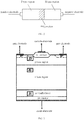
- FIG. 1 shows a structural schematic diagram of a conventional GCT unit.
- an existing conventional GCT unit mainly includes two parts: a GCT chip and a corresponding compact gate driver, wherein the interior of the GCT chip has a typical asymmetric structure, and PN junctions are set inside the GCT chip.
- the PN junctions are formed by manufacturing a P type semiconductor and an N type semiconductor on the same semiconductor substrate by different doping process and the diffusion action, wherein the semiconductor substrate is generally silicon or germanium, and a space charge region called PN junction is formed on an interface between the P type semiconductor and the N type semiconductor.
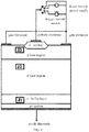
- FIG. 2 shows a structural schematic diagram of the PN junction according to the prior art.
- the PN junction has unidirectional conductivity, which is a characteristic used by many devices in the electronic technology.
- the PN junction constitutes the material basis of semiconductor diodes and bipolar transistors.
- a forward voltage is applied to the structure, a first PN junction J1 and a third PN junction J3 shown in FIG. 1 are forward biased and a second PN junction J2 is reverse biased.
- the structure can block several-kV voltage; however, when a reverse voltage is applied to the structure, the first PN junction J1 and the third PN junction J3 shown in FIG. 1 are reverse biased and the second PN junction J2 is forward biased.
- the blocking capability is only about 20 V.
- Zener breakdown or punch-through breakdown will occur in the first PN junction J1 under an extremely low reverse voltage. Therefore, when a reverse voltage is applied, the voltage mainly falls at the third PN junction J3; however, in the actual application situation, the GCT chip is used together with its gate driver, and the voltage distribution of the internal p base region or the n base region will be affected by the drive circuit.
- the control logic of the conventional gate driver is as follows: in a blocking state, the electric potential of cathode electrode is set 20V higher than that of gate electrode, thereby ensuring that the device is in a stable blocking state; and in an on state, drive current is injected from the gate electrode to the cathode electrode to trigger the device to conduct. At this time, in the on state or the blocking state, it is liable to damage the drive circuit by applying a reverse voltage to the whole IGCT/ETO device.
- power electronic devices In applications such as converters, power electronic devices generally need to have reverse conduction ability, which is usually implemented by an anti-paralleled diode outside the device or implementing the diode in a non-GCT region of the chip.
- antiparallel connection of the diode will introduce stray parameters in the loop to cause peak overvoltage and will increase the design difficulty of a press-fitting structure.
- Manufacturing the diode in the non-GCT region will reduce the current conducting capacity of the whole GCT chip and also will increase the difficulty of the process implementing process, which will greatly affect the yield.
- the present invention provides a device having a reverse conduction function.
- a device having a reverse conduction function includes: a GCT chip module and a drive circuit module, wherein the GCT chip module includes: a five-layer thyristor structure consisting of a p+ emitter , an n+ buffer layer, an n base region, a p base region and an n+ emitter , an anode electrode connected to the p+ emitter , a gate electrode connected to the p base region, and a cathode electrode connected to the n+ emitter ;
- the drive circuit module includes at least one of an IGCT drive circuit or an ETO drive circuit.
- the IGCT drive circuit includes: a changeover switch, a direct-current power supply and a trigger current source.
- the IGCT drive circuit forms four circuits between the cathode electrode and the gate electrode of the GCT chip module through the changeover switch, the direct-current power supply and the trigger current source, wherein the four circuits include:
- the ETO drive circuit includes: a first low-voltage MOSFET, a second low-voltage MOSFET and a trigger current source.
- the ETO drive circuit forms two circuits between the cathode electrode and the gate electrode of the chip module through the first low-voltage MOSFET, the second low-voltage MOSFET and the trigger current source, wherein the two circuits include:
- the GCT chip module is subjected to local life control processing.
- anode electrode, the cathode electrode and the gate electrode of the GCT chip module are all metal electrodes.
- the metal electrodes have thickness of 5 um to 30 um.
- the device provided by the present invention improves the characteristics of a GCT chip by doping an n+ buffer layer and a p+ emitter of a GCT chip module and by introducing a highly-doped p+ region below a gate electrode; and allows the GCT chip to be provided with a reverse conduction between a cathode electrode and the gate electrode by means of an IGCT drive circuit or an ETO drive circuit connected to the GCT chip module, thereby implementing a reverse conduction function of an IGCT or ETO device, and ensuring that the device is still provided with the performance of a conventional IGCT or ETO device during forward conduction.
- the device provided by the present invention implements the reverse conduction of the IGCT or ETO device, the process steps are simple, and the yield of industrial production is increased.
- the complexity of system design can be obviously reduced, higher efficiency is realized by single power electronic device, and the overall reliability of equipment is improved.
- the embodiment of the present invention provides a device having a reverse conduction function.
- the device includes a GCT chip module and a drive circuit module.
- the GCT chip module is provided with a five-layer thyristor structure consisting of a p+ emitter, an n+ buffer layer, an n base region, a p base region and an n+ emitter , an anode electrode connected to the p+ emitter , a gate electrode connected to the p base region, and a cathode electrode connected to the n+ emitter ;
- the GCT chip module has the same structure as the conventional GCT unit shown in FIG.
- a first PN junction J1 is formed in a doping region consisting of the p+ emitter and the n+ buffer layer, a second PN junction J2 is formed in the n base region, and a third PN junction J3 is formed in the p base region.
- the n+ buffer layer of the GCT chip module and the p+ emitter are doped, so that reversible and uniform avalanche breakdown or punch-through breakdown can occur in the first PN junction J1 under the condition of a reverse small voltage; furthermore, the GCT chip module is provided with a highly-doped p+ region below the gate electrode of the p base region, wherein the highly-doped p+ region specifically refers to a p+ doped region with concentration ranging from 10 17 /cm 3 to 10 21 /cm 3 , so that not only the low resistance characteristic during reverse conduction is ensured, but also the breakdown characteristic of the third PN junction J3 is not affected, as shown in FIG.
- the GCT chip module provided by the embodiment of the present invention also needs to preform local life control processing so as to improve the dynamic characteristic of the GCT chip module. For example: a part of structure in the GCT chip is subjected to 1-12MeV electron irradiation or proton irradiation, and a proper recombination center is brought into the GCT chip, thereby reducing the minority carrier lifetime in the GCT chip.
- the anode electrode, the cathode electrode and the gate electrode of the GCT chip module are all metal electrodes, wherein the metal electrodes are made of metal and have thickness of 5 um to 30 um, and the metal electrode structure can ensure that the GCT chip module has high lateral conduction capacity under the condition of large current.
- the drive circuit module is connected to the cathode electrode and the gate electrode in the GCT chip module through cables.
- the device provided by the embodiment of the present invention can form different circuits through the drive circuit module, so that the forward flow function of the device can be ensured, and the reverse conduction function of the device can be realized when the current direction is reversed.
- the drive circuit module includes an IGCT drive circuit or an ETO drive circuit, wherein the IGCT drive circuit and the GCT chip module are connected to form an IGCT device having a reverse conduction function, and the ETO drive circuit and the GCT chip module are connected to form an ETO device having a reverse conduction function.
- FIG. 4 shows a structural schematic diagram of an IGCT device having a reverse conduction function according to an embodiment of the present invention.
- the GCT chip module of the IGCT device is connected to the IGCT drive circuit;
- the IGCT drive circuit includes a changeover switch, a direct-current power supply and a trigger current source; and the IGCT drive circuit forms four circuits between the cathode electrode and the gate electrode of the GCT chip module through the changeover switch, the direct-current power supply and the trigger current source.
- the circuits which can be formed by the IGCT drive circuit include: 1. the cathode electrode and the gate electrode are directly connected to form short circuit; 2.
- FIG. 5 shows a structural schematic diagram of an ETO device having a reverse conduction function according to an embodiment of the present invention.
- the GCT chip module of the ETO device is connected to an ETO drive circuit, and the ETO drive circuit includes a first low-voltage MOSFET, a second low-voltage MOSFET and a trigger current source.
- the ETO drive circuit forms two circuits between the cathode electrode and the gate electrode of the GCT chip module through the first low-voltage MOSFET, the second low-voltage MOSFET and the trigger current source. Further, the circuits which can be formed by the ETO drive circuit includes: 1.
- an emitter of the first low-voltage MOSFET is connected to the cathode electrode, a collector of the first low-voltage MOSFET is connected to a negative electrode of the trigger current source, and a positive electrode of the trigger current source and the gate electrode are connected to form a path; 2. the emitter of the first low-voltage MOSFET is connected to the cathode electrode, the collector of the first low-voltage MOSFET is connected to a collector of the second low-voltage MOSFET, and an emitter of the second low-voltage MOSFET is connected to the gate electrode, thereby forming a forward flow path for injecting drive current from the gate electrode to the cathode electrode or forming short circuit between the gate electrode and the cathode electrode in a short time.
- the IGCT device forms connection of the cathode electrode of the GCT chip module and the negative electrode of the trigger current source and connection of the positive electrode of the trigger current source and the gate electrode through the IGCT drive circuit so as to form a reverse conduction path for injecting the drive current from the cathode electrode to the gate electrode
- the ETO device forms connection of the cathode electrode of the GCT chip module and the emitter of the first low-voltage MOSFET and connection of the collector of the first low-voltage MOSFET and the negative electrode of the trigger current source and connection of the positive electrode of the trigger current source and the gate electrode through the ETO drive circuit so as to form a reverse conduction path for injecting the drive current from the cathode electrode to the gate electrode
- the IGCT device or the ETO device has a reverse conduction function after the circuit having reverse flow is formed,.
- the IGCT drive circuit or the ETO drive circuit can identify the current direction of the anode electrode.
- There are three main methods for identifying the current direction of the anode electrode including: 1. comprehensive judgment is conducted by measuring a voltage between the gate electrode and the cathode electrode on a driver board and using the voltage and the internal trigger state of the driver; 2. an anode electrode current sensor is additionally mounted on the driver board for direct measurement; and 3. The voltage of the anode electrode and the cathode electrode is measured on the driver board, and the current direction of the anode electrode is measured and judged on the basis of the measured voltage.
- the IGCT drive circuit or the ETO drive circuit also can short-circuit the gate electrode and the cathode electrode of the GCT chip in a short time, thereby ensuring that the device will not be damaged by abnormal conduction.
- the IGCT drive circuit may form short circuit between the cathode electrode and the gate electrode of the GCT chip through the changeover switch; or the ETO drive circuit may form short circuit between the cathode electrode and the gate electrode of the GCT chip in a short time through the second low-voltage MOSFET.
- a low-resistance channel is formed between the gate electrode and the cathode electrode of the GCT chip by a method of forming short circuit.
- the gate electrode and the cathode electrode should maintain short circuit state, for example: the ETO drive circuit may form short circuit between the cathode electrode and the gate electrode of the chip by connecting a power electronic device or a relay on the second low-voltage MOSFET in parallel so as to cope with the possible abnormal reverse conduction situation and prolong the service life of the device.
- the device provided by the embodiment of the present invention improves the characteristics of a GCT chip with doping in n+ buffer layer and a p+ emitter of a GCT chip module and by preparing a highly-doped p+ region below a gate electrode; and allows the GCT chip to conduct reversely between a cathode electrode and the gate electrode by means of an IGCT drive circuit or an ETO drive circuit connected to the GCT chip module, thereby implementing a reverse conduction function of an IGCT or ETO device, and ensuring that the device is still provided with the performance of a conventional IGCT or ETO device during forward conduction.
- the device provided by the embodiment of the present invention implements the reverse conduction to the IGCT or ETO device, the process steps are simple, and the yield of industrial production is increased.
- the complexity of system design can be obviously reduced, higher efficiency is realized by single power electronic device, and the overall reliability of equipment is improved.
Landscapes
- Power Conversion In General (AREA)
Applications Claiming Priority (2)
| Application Number | Priority Date | Filing Date | Title |
|---|---|---|---|
| CN201811613543.5A CN109686783B (zh) | 2018-12-27 | 2018-12-27 | 一种具有反向通流功能的器件 |
| PCT/CN2019/104539 WO2020134177A1 (zh) | 2018-12-27 | 2019-09-05 | 一种具有反向通流功能的器件 |
Publications (2)
| Publication Number | Publication Date |
|---|---|
| EP3902011A1 true EP3902011A1 (de) | 2021-10-27 |
| EP3902011A4 EP3902011A4 (de) | 2022-02-09 |
Family
ID=66190602
Family Applications (1)
| Application Number | Title | Priority Date | Filing Date |
|---|---|---|---|
| EP19903618.7A Pending EP3902011A4 (de) | 2018-12-27 | 2019-09-05 | Bauteil mit umkehrstromfunktion |
Country Status (3)
| Country | Link |
|---|---|
| EP (1) | EP3902011A4 (de) |
| CN (1) | CN109686783B (de) |
| WO (1) | WO2020134177A1 (de) |
Families Citing this family (3)
| Publication number | Priority date | Publication date | Assignee | Title |
|---|---|---|---|---|
| CN109686783B (zh) * | 2018-12-27 | 2024-06-07 | 清华大学 | 一种具有反向通流功能的器件 |
| CN116387358B (zh) * | 2023-06-02 | 2023-08-01 | 清华大学 | 门极换流晶闸管及其制备方法 |
| CN118507519B (zh) * | 2024-06-21 | 2025-06-24 | 北京怀柔实验室 | 门极换流晶闸管及其制备方法、电子设备 |
Family Cites Families (14)
| Publication number | Priority date | Publication date | Assignee | Title |
|---|---|---|---|---|
| EP1298733A1 (de) * | 2001-09-28 | 2003-04-02 | ABB Schweiz AG | Abschaltbares Hochleistungsbauelement |
| JP2004288680A (ja) * | 2003-03-19 | 2004-10-14 | Mitsubishi Electric Corp | 圧接型半導体装置 |
| US8497552B2 (en) * | 2008-12-01 | 2013-07-30 | Cree, Inc. | Semiconductor devices with current shifting regions and related methods |
| CN201577025U (zh) * | 2009-07-31 | 2010-09-08 | Abb瑞士有限公司 | 用于功率半导体器件的控制器件 |
| CN101853878B (zh) * | 2010-06-03 | 2012-06-13 | 西安理工大学 | 一种pnp-沟槽复合隔离RC-GCT器件及制备方法 |
| CN103746002B (zh) * | 2013-12-17 | 2016-04-20 | 西安理工大学 | 一种台阶形沟槽-场限环复合终端结构 |
| EP2960941B1 (de) * | 2014-06-26 | 2017-01-04 | ABB Schweiz AG | Rückwärtsleitendes Hochleistungshalbleiterbauelement |
| CN104600101A (zh) * | 2015-02-03 | 2015-05-06 | 清华大学 | 一种集成门极换流晶闸管芯片的双门极接触环阴极面结构 |
| CN104795439B (zh) * | 2015-03-18 | 2017-07-18 | 清华大学 | 一种应用于混合式直流断路器的门极换流晶闸管芯片 |
| CN105590959B (zh) * | 2015-12-17 | 2018-05-29 | 清华大学 | 具有双p基区门阴极结构的门极换流晶闸管及其制备方法 |
| CN207367957U (zh) * | 2017-09-01 | 2018-05-15 | 清华大学 | 电气器件以及电气装置 |
| CN108718193B (zh) * | 2018-07-25 | 2024-06-25 | 清华大学 | 一种功率半导体元件的驱动保护电路及其控制方法 |
| CN109686783B (zh) * | 2018-12-27 | 2024-06-07 | 清华大学 | 一种具有反向通流功能的器件 |
| CN209544357U (zh) * | 2018-12-27 | 2019-10-25 | 清华大学 | 一种具有反向通流功能的器件 |
-
2018
- 2018-12-27 CN CN201811613543.5A patent/CN109686783B/zh active Active
-
2019
- 2019-09-05 WO PCT/CN2019/104539 patent/WO2020134177A1/zh not_active Ceased
- 2019-09-05 EP EP19903618.7A patent/EP3902011A4/de active Pending
Also Published As
| Publication number | Publication date |
|---|---|
| EP3902011A4 (de) | 2022-02-09 |
| CN109686783B (zh) | 2024-06-07 |
| WO2020134177A1 (zh) | 2020-07-02 |
| CN109686783A (zh) | 2019-04-26 |
Similar Documents
| Publication | Publication Date | Title |
|---|---|---|
| JP6698746B2 (ja) | 半導体デバイス | |
| US10153275B2 (en) | Method of operating an IGBT having switchable and non-switchable diode cells | |
| CN114188396B (zh) | 一种绝缘栅双极晶体管及其制造方法、电子设备 | |
| EP3902011A1 (de) | Bauteil mit umkehrstromfunktion | |
| CN108336085B (zh) | 一种栅极嵌入小岛式可控硅静电防护器件 | |
| JP7151902B2 (ja) | 半導体装置 | |
| CN102270640A (zh) | 大电流整晶圆全压接平板式封装的igbt及其制造方法 | |
| CN104600101A (zh) | 一种集成门极换流晶闸管芯片的双门极接触环阴极面结构 | |
| US10950690B2 (en) | Power electronic arrangement | |
| CN109686787B (zh) | 一种利用二极管钳位的具有载流子存储层的igbt器件 | |
| CN119997615B (zh) | 一种高可靠高压驱动芯片的静电浪涌一体化防护电路 | |
| CN109742139B (zh) | 一种基于ligbt的单栅控制电压电流采样器件 | |
| CN203179900U (zh) | 一种快恢复二极管frd芯片 | |
| JPH03225960A (ja) | 半導体デバイス | |
| CN112614836B (zh) | 一种防护型半导体器件 | |
| CN212161818U (zh) | 用于过压击穿功能的缓冲区变掺杂结构及半导体器件 | |
| CN110504312B (zh) | 一种具有短路自保护能力的横向igbt | |
| CN209544357U (zh) | 一种具有反向通流功能的器件 | |
| CN211930611U (zh) | 一种可控硅驱动电路及可控硅芯片 | |
| CN111464166B (zh) | 一种可控硅驱动电路及可控硅芯片 | |
| CN110504259B (zh) | 一种具有过流保护能力的横向igbt | |
| CN118315997A (zh) | GaN基增强型HEMT的ESD保护电路 | |
| CN111627904B (zh) | 一种具有vdmos和晶闸管的可编程过电压保护器件 | |
| WO2017063320A1 (zh) | 一种高鲁棒性的高压静电放电保护器件 | |
| RU91222U1 (ru) | Мощный интегральный тиристор с полевым управлением |
Legal Events
| Date | Code | Title | Description |
|---|---|---|---|
| STAA | Information on the status of an ep patent application or granted ep patent |
Free format text: STATUS: THE INTERNATIONAL PUBLICATION HAS BEEN MADE |
|
| PUAI | Public reference made under article 153(3) epc to a published international application that has entered the european phase |
Free format text: ORIGINAL CODE: 0009012 |
|
| STAA | Information on the status of an ep patent application or granted ep patent |
Free format text: STATUS: REQUEST FOR EXAMINATION WAS MADE |
|
| 17P | Request for examination filed |
Effective date: 20210719 |
|
| AK | Designated contracting states |
Kind code of ref document: A1 Designated state(s): AL AT BE BG CH CY CZ DE DK EE ES FI FR GB GR HR HU IE IS IT LI LT LU LV MC MK MT NL NO PL PT RO RS SE SI SK SM TR |
|
| A4 | Supplementary search report drawn up and despatched |
Effective date: 20220110 |
|
| RIC1 | Information provided on ipc code assigned before grant |
Ipc: H01L 29/423 20060101ALN20220103BHEP Ipc: H01L 29/10 20060101ALI20220103BHEP Ipc: H03K 17/567 20060101ALI20220103BHEP Ipc: H01L 29/744 20060101ALI20220103BHEP Ipc: H01L 29/08 20060101ALI20220103BHEP Ipc: H01L 29/06 20060101AFI20220103BHEP |
|
| DAV | Request for validation of the european patent (deleted) | ||
| DAX | Request for extension of the european patent (deleted) | ||
| STAA | Information on the status of an ep patent application or granted ep patent |
Free format text: STATUS: EXAMINATION IS IN PROGRESS |
|
| 17Q | First examination report despatched |
Effective date: 20241029 |
|
| REG | Reference to a national code |
Ref country code: DE Ref legal event code: R079 Free format text: PREVIOUS MAIN CLASS: H01L0029060000 Ipc: H10D0018600000 |
|
| GRAP | Despatch of communication of intention to grant a patent |
Free format text: ORIGINAL CODE: EPIDOSNIGR1 |
|
| STAA | Information on the status of an ep patent application or granted ep patent |
Free format text: STATUS: GRANT OF PATENT IS INTENDED |
|
| RIC1 | Information provided on ipc code assigned before grant |
Ipc: H10D 18/60 20250101AFI20260306BHEP Ipc: H10D 62/17 20250101ALI20260306BHEP Ipc: H10D 62/53 20250101ALI20260306BHEP Ipc: H10D 64/27 20250101ALI20260306BHEP Ipc: H03K 17/567 20060101ALI20260306BHEP |
|
| INTG | Intention to grant announced |
Effective date: 20260318 |