EP3874308B1 - Verfahren und vorrichtung zur steuerung und unterdrückung von streulicht in einer fotonischen integrierten schaltung - Google Patents
Verfahren und vorrichtung zur steuerung und unterdrückung von streulicht in einer fotonischen integrierten schaltung Download PDFInfo
- Publication number
- EP3874308B1 EP3874308B1 EP19813702.8A EP19813702A EP3874308B1 EP 3874308 B1 EP3874308 B1 EP 3874308B1 EP 19813702 A EP19813702 A EP 19813702A EP 3874308 B1 EP3874308 B1 EP 3874308B1
- Authority
- EP
- European Patent Office
- Prior art keywords
- stray light
- waveguide
- guided
- light
- optic device
- Prior art date
- Legal status (The legal status is an assumption and is not a legal conclusion. Google has not performed a legal analysis and makes no representation as to the accuracy of the status listed.)
- Active
Links
Images


Classifications
-
- G—PHYSICS
- G02—OPTICS
- G02B—OPTICAL ELEMENTS, SYSTEMS OR APPARATUS
- G02B6/00—Light guides; Structural details of arrangements comprising light guides and other optical elements, e.g. couplings
- G02B6/10—Light guides; Structural details of arrangements comprising light guides and other optical elements, e.g. couplings of the optical waveguide type
- G02B6/12—Light guides; Structural details of arrangements comprising light guides and other optical elements, e.g. couplings of the optical waveguide type of the integrated circuit kind
- G02B6/12004—Combinations of two or more optical elements
-
- G—PHYSICS
- G01—MEASURING; TESTING
- G01C—MEASURING DISTANCES, LEVELS OR BEARINGS; SURVEYING; NAVIGATION; GYROSCOPIC INSTRUMENTS; PHOTOGRAMMETRY OR VIDEOGRAMMETRY
- G01C19/00—Gyroscopes; Turn-sensitive devices using vibrating masses; Turn-sensitive devices without moving masses; Measuring angular rate using gyroscopic effects
- G01C19/58—Turn-sensitive devices without moving masses
-
- G—PHYSICS
- G02—OPTICS
- G02B—OPTICAL ELEMENTS, SYSTEMS OR APPARATUS
- G02B6/00—Light guides; Structural details of arrangements comprising light guides and other optical elements, e.g. couplings
- G02B6/10—Light guides; Structural details of arrangements comprising light guides and other optical elements, e.g. couplings of the optical waveguide type
- G02B6/12—Light guides; Structural details of arrangements comprising light guides and other optical elements, e.g. couplings of the optical waveguide type of the integrated circuit kind
- G02B6/122—Basic optical elements, e.g. light-guiding paths
-
- H—ELECTRICITY
- H10—SEMICONDUCTOR DEVICES; ELECTRIC SOLID-STATE DEVICES NOT OTHERWISE PROVIDED FOR
- H10F—INORGANIC SEMICONDUCTOR DEVICES SENSITIVE TO INFRARED RADIATION, LIGHT, ELECTROMAGNETIC RADIATION OF SHORTER WAVELENGTH OR CORPUSCULAR RADIATION
- H10F55/00—Radiation-sensitive semiconductor devices covered by groups H10F10/00, H10F19/00 or H10F30/00 being structurally associated with electric light sources and electrically or optically coupled thereto
-
- G—PHYSICS
- G02—OPTICS
- G02B—OPTICAL ELEMENTS, SYSTEMS OR APPARATUS
- G02B6/00—Light guides; Structural details of arrangements comprising light guides and other optical elements, e.g. couplings
- G02B6/10—Light guides; Structural details of arrangements comprising light guides and other optical elements, e.g. couplings of the optical waveguide type
- G02B6/12—Light guides; Structural details of arrangements comprising light guides and other optical elements, e.g. couplings of the optical waveguide type of the integrated circuit kind
- G02B2006/12083—Constructional arrangements
- G02B2006/12116—Polariser; Birefringent
-
- G—PHYSICS
- G02—OPTICS
- G02B—OPTICAL ELEMENTS, SYSTEMS OR APPARATUS
- G02B6/00—Light guides; Structural details of arrangements comprising light guides and other optical elements, e.g. couplings
- G02B6/10—Light guides; Structural details of arrangements comprising light guides and other optical elements, e.g. couplings of the optical waveguide type
- G02B6/12—Light guides; Structural details of arrangements comprising light guides and other optical elements, e.g. couplings of the optical waveguide type of the integrated circuit kind
- G02B2006/12083—Constructional arrangements
- G02B2006/12119—Bend
-
- G—PHYSICS
- G02—OPTICS
- G02B—OPTICAL ELEMENTS, SYSTEMS OR APPARATUS
- G02B6/00—Light guides; Structural details of arrangements comprising light guides and other optical elements, e.g. couplings
- G02B6/10—Light guides; Structural details of arrangements comprising light guides and other optical elements, e.g. couplings of the optical waveguide type
- G02B6/12—Light guides; Structural details of arrangements comprising light guides and other optical elements, e.g. couplings of the optical waveguide type of the integrated circuit kind
- G02B2006/12083—Constructional arrangements
- G02B2006/12126—Light absorber
-
- G—PHYSICS
- G02—OPTICS
- G02B—OPTICAL ELEMENTS, SYSTEMS OR APPARATUS
- G02B6/00—Light guides; Structural details of arrangements comprising light guides and other optical elements, e.g. couplings
- G02B6/10—Light guides; Structural details of arrangements comprising light guides and other optical elements, e.g. couplings of the optical waveguide type
- G02B6/12—Light guides; Structural details of arrangements comprising light guides and other optical elements, e.g. couplings of the optical waveguide type of the integrated circuit kind
- G02B2006/12133—Functions
- G02B2006/12147—Coupler
-
- G—PHYSICS
- G02—OPTICS
- G02B—OPTICAL ELEMENTS, SYSTEMS OR APPARATUS
- G02B6/00—Light guides; Structural details of arrangements comprising light guides and other optical elements, e.g. couplings
- G02B6/10—Light guides; Structural details of arrangements comprising light guides and other optical elements, e.g. couplings of the optical waveguide type
- G02B6/12—Light guides; Structural details of arrangements comprising light guides and other optical elements, e.g. couplings of the optical waveguide type of the integrated circuit kind
- G02B2006/12166—Manufacturing methods
- G02B2006/12195—Tapering
-
- G—PHYSICS
- G02—OPTICS
- G02B—OPTICAL ELEMENTS, SYSTEMS OR APPARATUS
- G02B6/00—Light guides; Structural details of arrangements comprising light guides and other optical elements, e.g. couplings
- G02B6/10—Light guides; Structural details of arrangements comprising light guides and other optical elements, e.g. couplings of the optical waveguide type
- G02B6/12—Light guides; Structural details of arrangements comprising light guides and other optical elements, e.g. couplings of the optical waveguide type of the integrated circuit kind
- G02B6/122—Basic optical elements, e.g. light-guiding paths
- G02B6/1228—Tapered waveguides, e.g. integrated spot-size transformers
-
- G—PHYSICS
- G02—OPTICS
- G02B—OPTICAL ELEMENTS, SYSTEMS OR APPARATUS
- G02B6/00—Light guides; Structural details of arrangements comprising light guides and other optical elements, e.g. couplings
- G02B6/10—Light guides; Structural details of arrangements comprising light guides and other optical elements, e.g. couplings of the optical waveguide type
- G02B6/12—Light guides; Structural details of arrangements comprising light guides and other optical elements, e.g. couplings of the optical waveguide type of the integrated circuit kind
- G02B6/122—Basic optical elements, e.g. light-guiding paths
- G02B6/125—Bends, branchings or intersections
-
- G—PHYSICS
- G02—OPTICS
- G02B—OPTICAL ELEMENTS, SYSTEMS OR APPARATUS
- G02B6/00—Light guides; Structural details of arrangements comprising light guides and other optical elements, e.g. couplings
- G02B6/10—Light guides; Structural details of arrangements comprising light guides and other optical elements, e.g. couplings of the optical waveguide type
- G02B6/12—Light guides; Structural details of arrangements comprising light guides and other optical elements, e.g. couplings of the optical waveguide type of the integrated circuit kind
- G02B6/126—Light guides; Structural details of arrangements comprising light guides and other optical elements, e.g. couplings of the optical waveguide type of the integrated circuit kind using polarisation effects
Definitions
- a photonic integrated circuit is suitable for mass production and can achieve a significant economy of scale. Silicon-based PICs may benefit from well-developed fabrication experience, technology, and scalability already for silicon-based microelectronics industry.
- a PIC may comprise two or more optical components integrated on a same substrate, for example a semiconductor wafer.
- the optic components may perform different or same functions (e.g., splitter, combiner, coupler, interferometer, modulator, filter, isolator, delay line, among others) to build an optical system.
- Optic waveguides may be utilized to link the optic components to conduct optical signals between them. The components may be connected in parallel or in series.
- Non-guided stray light in radiation mode may be generated by the individual components or by waveguides.
- the stray light source may be a Y-junction combiner, such as is implemented at the output end of an integrated Mach-Zehnder interferometer used in an optical modulator, or for a Sagnac interferometer used in a fiber optic gyroscope.
- the stray light source may be a Y-junction combiner, such as is implemented at the output end of an integrated Mach-Zehnder interferometer used in an optical modulator, or for a Sagnac interferometer used in a fiber optic gyroscope.
- the non-guided stray light may stay in the same plane of the optical system or may be reflected and refracted back to the same plane at interfaces.
- a stray light source may be radiation modes generated at bended waveguides. This type of stay light source may occur in a filter comprising micro-ring waveguide resonators, or a polarizer comprising cascade of bending waveguides. Light may become non-guided and radiated into the substrate either in the operation polarization mode or in the orthogonal polarization mode due to the bending radiations.
- the stray light may be recoupled by the later circuit or the neighboring components. When the recoupled light joins with the desired optic signal, an erroneous signal may be generated.
- the optic system comprising a PIC may be constructed for applications that require stable output polarization state. These applications may include optic interferometric modulators, optic interferometric sensors, wavelength-division multiplexing, and coherent communication. Optic birefringence may be deliberately introduced into the components and waveguides. The waveguides and components may conduct and process light of a single linear polarization. To generate and maintain the light in a signal linear polarization state, a polarizer may be included into a PIC.
- An optic interferometer may be a hybrid fiber optic gyroscope comprising a PIC and optic fiber coil.
- Another example of an optic interferometer may be an optic coherence tomographic system.
- Erroneous signal may be produced due to a formation of parasitic interferences.
- Light in radiation mode that is recoupled into the circuit may coherently interfere with the desired signal.
- the recoupled light that is originally in the orthogonal polarization mode may be cross coupled into the operation polarization mode and results in interference type of errors.
- the publication JP2012215901 discloses an optical waveguide device capable of highly efficiently guiding unnecessary light outside a substrate or outside an entire optical waveguide even when optical waveguides are integrated.
- the optical waveguide device comprises on a substrate, an optical waveguide formed by thermally diffusing a material with a high refractive index, and the optical waveguide includes a main waveguide for propagating signal light, and unnecessary-light waveguides for removing unnecessary light from the main waveguide.
- the unnecessary-light waveguides are configured to remove high-order mode light propagating the main waveguide from the main waveguide as the unnecessary light and to guide it outside the substrate or outside the entire optical waveguide, and the unnecessary-light waveguides are parted by the main waveguide on both sides thereof at an intersection part where the unnecessary-light waveguides and the main waveguide intersect.
- the embodiments described herein are directed to a photonic integrated circuit (PIC) that mitigates detrimental effects of stray light generated by one or more components of the PIC.
- the PIC comprises a substrate that has an optical device integrated onto the substrate.
- the integrated optical device may comprise, for example, a Y-junction, a waveguide-to-optical fiber coupling, and/or a polarizer, among others.
- the described embodiments are directed to apparatus configured to collect and selectively direct stray light from the optical device to a facility capable of mitigating the stray light by, for example, converting the stray light into heat, although other techniques for mitigating the stray light may alternatively be used.
- a hybrid photonic integrated circuit may be constructed to expand the functionality of an integrated optic system.
- the HPIC may be constructed by bonding together several integrated chips. These integrated chips may be optic, electrooptic, or optoelectronic chips, or may be optic chips made of different materials, or optic chips fabricated with two or more different processes. Electronic chips may also be attached to optoelectronic or electrooptic chips and electrically coupled by, for example, solder bumps or wire-bonds. Optic fibers may be attached to the optic, electrooptic, or optoelectronic chips. The methods of the attachment may be direct-coupling between two polished facets, using an optic lens for mode conversion, shaping a micro-lens at a fiber tip, or fabricating a surface grating coupler. Non-guided stray light may be produced in a HPIC. Stray light may be generated at the transition area where waveguides on the two bonded chips been connected.
- stray light may still result due to possible differences of the dimensions and effective refractive indices of the two connected waveguides. Stray light may be produced at the connection interface of end-fired coupling between two integrated chips, or between an integrated chip and an optic fiber. Scatter light may escape the core of the waveguide due to an optic misalignment of the input optic mode, or an optic mode-field mismatching of the two connected waveguides. The non-overlapped portion of the fiber mode fields may be non-guided and scattered across the area of photonic integrated circuit. An HPIC integrated with optoelectronic chips may be more susceptible to receiving erroneous signal.
- Components that particularly sensitive to stray light may be light generating electrooptic components such as optic amplifiers and lasers, light receiving optoelectronic components such as photodetectors, and phase sensitive components such as interferometers. Stray light, if allowed to freely propagate within the substrate and to reflect from the substrate surfaces, may interfere with the proper operation of the optic system.
- a higher degree of integration of PICs or HPICs may be implemented to reduce the size, or lower the cost, of an optic system.
- the high degree of integration may be achievable by reducing the size of the PICs or introducing more functional components into PICs, so a larger number of PICs or PICs with more functions can be fitted in a same semiconductor wafer.
- Optic components may be placed closer to realize the function expansion and the size reduction. However, stray light generation and reception may become more notable if the optic components are more closely located. Light scattered from one component may be readily coupled to a nearby component and generate the erroneous signal in that component, degrading its optic performance.
- the invention provides a photonic integrated circuit (PIC) according to claim 1.
- PIC photonic integrated circuit
- the invention provides a photonic integrated circuit (PIC) according to claim 10.
- PIC photonic integrated circuit
- the invention provides a method of mitigating stray light generated on a photonic integrated circuit (PIC) according to claim 12.
- PIC photonic integrated circuit
- a photonic integrated circuit may comprise a substrate that has an optical device integrated onto the substrate.
- the integrated optical device may comprise, for example, a Y-junction, a waveguide-to-optical fiber coupling, and/or a polarizer, among others.
- the described embodiments may be directed to apparatus configured to collect and selectively direct stray light from the optical device to a facility capable of mitigating the stray light by, for example, converting the stray light into heat, although other techniques for mitigating the stray light may alternatively be used.
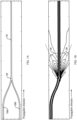
- a photonic integrated circuit may have a Y-junction, built on a substrate, that comprises a common base waveguide 102, a splitting waveguide structure, and two branch waveguides 106a, 106b.
- the light propagates in one of the branch waveguides from left to right.
- part of the light power may continue to be guided and to propagate in the common base waveguide in a single mode if the waveguide is a single mode waveguide.
- Another part of the optic power of the input light may be in an asymmetrical mode after passing through the splitting waveguide structure 104 and is not guided but is rather radiated out from the waveguide into the substrate.
- FIG. 1B shows a two-dimensional contour plot of the light power distribution in the Y-junction area, including the light in asymmetric mode radiated out from the splitting waveguide structure.
- the non-guided stray light spreads out along angles 108 above and below the common base waveguide 102.
- the radiation light may be recoupled or received by any components in the path of the radiation, which may add erroneous signal to the desired signal. It is desirable, therefore, to prevent the stray light from reaching such in-path circuits or neighboring components.
- Various techniques have been suggested to suppress stray light, including deep etched trenches filled with an absorbing material, light shields built with metal walls and doped semiconductor regions, the open mouth of an optical trap, and light absorbing films.
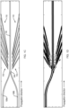
- an integrated Y-junction may be built on a substrate with an array of collectors.
- the array of collectors 110 may be made from the same materials and fabricated with the same processes as the main circuit waveguide structure.
- the array of collectors 110 may be arranged such that the collectors are aligned in the direction that the stray light is radiated out from the junction, depicted in FIG. 1B .
- the array of collectors 110 may be directed as fanning out, as shown in FIG. 1C .
- the tips of the collectors that are directed to the junction area may be optimized into a shape to improve the efficiency for receiving the stray light.
- the mode-field size may be enlarged by using the forward taper, which has a waveguide core increased gradually in size at the waveguide tip either in horizontal, or in vertical direction or in both directions.
- the mode-field size may also be enlarged by using an inverse taper, in which the waveguide core is reduced gradually in size either in the horizontal direction, or in vertical direction, or in both directions.
- a forward taper may be used to increase the mode-size when the index difference of refractions ( ⁇ n) between the core and cladding materials is small, such as ⁇ n ⁇ 0.1, so the increase of waveguide core size may not readily facilitate supporting a high-order mode, which would increase the propagation loss.
- an inverse taper is often used in a waveguide that has a large index difference between the core material and the cladding material, such as ⁇ n larger than 0.5.
- Examples of such waveguides may include a waveguide with silicon nitride core and silicon oxide cladding or a silicon-on-insulator (SOI) waveguide.
- the non-guided light that is sourced at the junction 104 may be collected and guided by the array of the waveguide collectors 110, as demonstrated by the contour plot of the light power distribution shown in FIG. 1D .
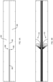
- the stray light collected by the waveguide collectors 110 is further guided by secondary waveguides 202 towards damping areas 204, where the light energy may be converted into heat and dissipated thermal-conductively, as shown in FIG. 2 .
- the optic dampers 204 may comprise an area where the evanescent waves of each of the secondary waveguides 202 are exposed for a length l at the ends of the waveguides 202, and light energy absorptive material being filled in the exposed area so that the exposed waveguide sections are covered with the absorptive material.
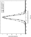
- More than 20dB suppression of the stray light may be achievable using the collectors 110 of the described embodiments. As shown in FIGs. 3A and 3B , approximately 12dB suppression of the stray light was measured on an example ultrathin silicon nitride waveguide after placing six collectors on each side of a Y-junction.
- an example of a PIC may comprise a photonic integrated circuit having a waveguide 402 built on a substrate 404 and an optic fiber 406.
- the waveguide 402 may have its end 408 optimized to connect to the optic fiber 406.
- the mode-field dimensions of the integrated waveguide 402 and the fiber 406 may not be matching and, therefore, non-guided stray light 410 may radiate out from the waveguide-fiber joint point 409 into the cladding layer of waveguides and substrate 404 of the PIC, as shown in a simulated result in FIG.4B .
- the radiated stray light 410 (shown in FIG.
- a described PIC may have an array of collectors 420 that may be made from the same materials and fabricated using the same processes as the waveguides 402 of the main optic circuit.
- the collectors 420 may be arranged in such a way that the collectors 420 are aligned in the direction that the stray light radiates out from the joint point 409.
- a plurality of collectors may be employed so that the collectors 420 may be arranged in a fanned-out configuration, as shown in FIG. 4C .
- the tips of the collectors 412 that are arranged to be pointing to the joint point may be optimized into a shape to improve the efficiency for receiving the radiated stray light.
- tapering the tips of the collectors 412 is beneficial due to the enlarged mode-field size that occurs at the tips of the collectors.
- the mode-field size may be enlarged by using the forward taper or may be enlarged by using an inverse taper.
- the non-guided light generated at the joint point 409 may then be collected by the waveguide collector array 412, as shown in FIG. 4D .
- the stray light collected by the waveguide collector array 412 is guided continuously by secondary waveguides, which are linking to the back ends of the collector waveguides respectively, and led towards damping areas where absorption materials may be utilized, such as the dampers 204 depicted in FIG. 2 with respect to the Y-junction arrangement. More than 20dB suppression of the stray light may be achievable by using the collector arrays of the described embodiments.
- an example embodiment of a PIC may comprise a birefringent waveguide, or a cascade of birefringent waveguides, each being curved at least to some extent.
- the waveguides 502 are in the shape of a half circle, although other curved arrangements may alternatively be used.
- the example waveguides 502 may be built on a substrate and arranged to be coupled in series, as shown in FIG. 5 , to form an "m" shape.
- the birefringence of the waveguides 502 may result in a higher confinement of light propagating in a transverse electric (TE) polarization mode than light propagating in a transverse magnetic (TM) mode.
- TE transverse electric
- TM transverse magnetic
- each of the half circle waveguides 502 may be optimized such that the waveguides 502 guide the TE polarization light with a low propagation loss, while imposing a large bending loss on the light in TM mode.
- the series of the half circles therefore, cumulatively constitute a polarizer with a high propagation extinction ratio (PER).
- the TM polarization-mode light may be not completely guided by the waveguide 502 and may be radiated into the substrate and cladding layer of the waveguides 502.
- the non-guided light may be recoupled back into the optic circuit, which may add light power in the TM mode of the waveguide, and effectively degrade the polarizer.
- a series of the collector waveguides 504 may be placed alongside with the curved waveguide sections 502 as indicated in FIG. 5 .
- the collector waveguides 504 may be aligned in the direction of the tangent lines of the curvature of the polarizer waveguide. As for the collectors described with respect to FIGs.
- the tips of collectors 504 may be optimized in shape to improve the efficiency for receiving the coming stray light. Tapering the tips of the collectors is utilized to enlarge the mode-field size at the tip of the collectors.
- the mode-field size may be enlarged by using the forward taper or may be enlarged by using an inverse taper.
- the stray light collected by the waveguide collectors 504 is guided by secondary waveguides 506 towards damping areas 508, where absorption materials may be utilized.
Landscapes
- Physics & Mathematics (AREA)
- Engineering & Computer Science (AREA)
- General Physics & Mathematics (AREA)
- Microelectronics & Electronic Packaging (AREA)
- Optics & Photonics (AREA)
- Radar, Positioning & Navigation (AREA)
- Remote Sensing (AREA)
- Optical Integrated Circuits (AREA)
Claims (12)
- Photonische integrierte Schaltung, PIC, umfassend:eine integrierte optische Vorrichtung, die auf einem Substrat angeordnet ist;
undeine integrierte optische Struktur, die auf dem Substrat um die integrierte optische Vorrichtung herum angeordnet ist, wobei die integrierte optische Struktur Folgendes umfasst:eine Anordnung von Streulichtkollektoren (110, 412, 504), die angeordnet sind, um das von der integrierten optischen Vorrichtung erzeugte nicht geleitete Streulicht zu sammeln, wobei jeder Streulichtkollektor (110, 412, 504) ferner einen Wellenleiter (110, 412, 504) umfasst, der Streulicht sammelt, der Wellenleiter (110, 412, 504) ein erstes Ende und ein zweites Ende aufweist, wobei das erste Ende proximal zu der integrierten optischen Vorrichtung angeordnet ist und das zweite Ende mit einem sekundären Wellenleiter (202, 506) verbunden ist, sodass das Streulicht kontinuierlich von dem Streulichtkollektoren (110, 412, 504) zu dem sekundären Wellenleiter (202, 506) geleitet wird; undeinen Lichtdämpfer, der konfiguriert ist, um das von der Anordnung von Streulichtkollektoren (110, 412, 504) gesammelte nicht geleitete Streulicht zu empfangen und das nicht geleitete Streulicht abzuschwächen;wobei jeder sekundäre Wellenleiter (202, 506) kontinuierlich gesammeltes Streulicht zu dem Lichtdämpfer leitet,wobei das erste Ende von jedem Wellenleiter (110, 412, 504) verjüngt ist, um eine Modenfeldgröße zu vergrößern, und sich das nicht geleitete Streulicht entlang eines Pfads propagiert, und die Anordnung von Streulichtkollektoren (110, 412, 504) in dem Pfad angeordnet ist, um mit einer Propagationsrichtung des nicht geleiteten Streulichts ausgerichtet zu sein und konfiguriert ist, um ein Empfangen des nicht geleiteten Streulichts in das erste Ende des Wellenleiters (110, 412, 504) zu erleichtern. - PIC nach Anspruch 1, wobei die integrierte optische Struktur erste Materialien umfasst, die integrierte optische Vorrichtung zweite Materialien umfasst und die ersten Materialien gleich wie die zweiten Materialien sind.
- PIC nach Anspruch 1, wobei die integrierte optische Struktur und die integrierte optische Vorrichtung monolithisch auf dem Substrat angefertigt sind.
- PIC nach Anspruch 1, wobei die integrierte optische Vorrichtung auf das Substrat geklebt ist und die integrierte optische Vorrichtung eine lichtemittierende Vorrichtung ist.
- PIC nach Anspruch 1, wobei die integrierte optische Vorrichtung einen integrierten Y-Übergang umfasst.
- PIC nach Anspruch 1, wobei die integrierte optische Vorrichtung einen integrierten Polarisator umfasst, der eine Kaskade von einem oder mehreren optisch gekoppelten gebogenen Wellenleitern ist.
- PIC nach Anspruch 1, wobei die integrierte optische Vorrichtung einen integrierten Polarisator umfasst, und wobei der integrierte Polarisator ein Filter ist, der einen oder mehrere Mikroring-Wellenleiterresonatoren umfasst.
- PIC nach Anspruch 1, wobei der Lichtdämpfer lichtabsorbierendes Material umfasst.
- PIC nach Anspruch 1, wobei der Lichtdämpfer Metallmaterial umfasst.
- Photonische integrierte Schaltung, PIC, umfassend:eine integrierte optische Vorrichtung, die auf einem Substrat angeordnet ist;eine zweite optische Vorrichtung, die auf dem Substrat angeordnet und an einer Kopplungsstelle mit der integrierten optischen Vorrichtung gekoppelt ist; undeine integrierte optische Struktur, die auf dem Substrat um die Kopplungsverbindung herum angeordnet ist, wobei die integrierte optische Struktur Folgendes umfasst:eine Anordnung von Streulichtkollektoren (110, 412, 504), die angeordnet sind, um nicht geleitetes Streulicht zu sammeln, das von einem oder mehreren von (i) der integrierten optischen Vorrichtung, (ii) der zweiten optischen Vorrichtung und (iii) der Kopplungsverbindung erzeugt wird; undeinen Lichtdämpfer, der konfiguriert ist, um das von der Anordnung von Streulichtkollektoren (110, 412, 504) gesammelte nicht geleitete Streulicht zu empfangen und das nicht geleitete Streulicht abzuschwächen;wobei jeder Streulichtkollektor (110, 412, 504) weiterhin einen Wellenleiter (110, 412, 504) umfasst, der Streulicht sammelt, der Wellenleiter (110, 412, 504) ein erstes Ende und ein zweites Ende aufweist, das erste Ende proximal zu der integrierten optischen Vorrichtung, der zweiten optischen Vorrichtung und der Kopplungsverbindung angeordnet ist und das zweite Ende mit einem sekundären Wellenleiter (202, 506) verbunden ist, sodass das Streulicht kontinuierlich von dem Streulichtkollektor (110, 412, 504) zu dem sekundären Wellenleiter (202, 506) geleitet wird und jeder sekundäre Wellenleiter (202, 506) kontinuierlich gesammeltes Streulicht zu dem Lichtdämpfer leitet;wobei das erste Ende von jedem Wellenleiter (110, 412, 504) verjüngt ist, um eine Modenfeldgröße zu vergrößern, und sich das nicht geleitete Streulicht entlang eines Pfads propagiert, und die Anordnung von Streulichtkollektoren (110, 412, 504) in dem Pfad angeordnet ist, um mit einer Propagationsrichtung des nicht geleiteten Streulichts ausgerichtet zu sein und konfiguriert ist, um ein Empfangen des nicht geleiteten Streulichts in das erste Ende des Wellenleiters (10, 412, 504) zu erleichtern.
- PIC nach Anspruch 10, wobei die integrierte optische Struktur erste Materialien umfasst, die integrierte optische Vorrichtung zweite Materialien umfasst und die ersten Materialien gleich wie die zweiten Materialien sind.
- Verfahren zum Abschwächen von Streulicht, das auf einer photonischen integrierten Schaltung, PIC, erzeugt wird, umfassend:Sammeln, durch eine Anordnung von Streulichtkollektoren (110, 412, 504), von nicht geleitetem Streulicht, das von einer integrierten optischen Vorrichtung erzeugt wird, die auf einem Substrat der PIC angeordnet ist; undFördern, durch die Anordnung von Streulichtkollektoren (110, 412, 504), des gesammelten Streulichts zu einem Lichtdämpfer, der konfiguriert ist, um das von der Anordnung von Streulichtkollektoren (110, 412, 504) gesammelte nicht geleitete Streulicht zu empfangen und das nicht geleitete Streulicht abzuschwächen;wobei jeder Streulichtkollektor (110, 412, 504) weiterhin einen Wellenleiter (110, 412, 504) umfasst, der Streulicht sammelt, der Wellenleiter (110, 412, 504) ein erstes Ende und ein zweites Ende aufweist, wobei das erste Ende proximal zu der integrierten optischen Vorrichtung angeordnet ist und das zweite Ende mit einem sekundären Wellenleiter (202, 506) verbunden ist, sodass das Streulicht kontinuierlich von dem Streulichtkollektoren (110, 412, 504) zu dem sekundären Wellenleiter (202, 506) geleitet wird, und jeder sekundäre Wellenleiter (202, 506) kontinuierlich gesammeltes Streulicht zu dem Lichtdämpfer leitet;das Verfahren ferner umfassend ein Anordnen der Anordnung von Streulichtkollektoren (110, 412, 504) in einem Pfad, entlang dessen sich das nicht geleitete Streulicht propagiert, wobei die Anordnung von Streulichtkollektoren (110, 412, 504) mit einer Propagationsrichtung des nicht geleiteten Streulichts ausgerichtet ist, wobei das erste Ende von jedem Wellenleiter (110, 412, 504) verjüngt ist, um eine Modenfeldgröße zu vergrößern.
Applications Claiming Priority (2)
| Application Number | Priority Date | Filing Date | Title |
|---|---|---|---|
| US201862753430P | 2018-10-31 | 2018-10-31 | |
| PCT/US2019/059195 WO2020092789A1 (en) | 2018-10-31 | 2019-10-31 | Method and apparatus for control and suppression of stray light in a photonic integrated circuit |
Publications (2)
| Publication Number | Publication Date |
|---|---|
| EP3874308A1 EP3874308A1 (de) | 2021-09-08 |
| EP3874308B1 true EP3874308B1 (de) | 2025-03-26 |
Family
ID=68766850
Family Applications (1)
| Application Number | Title | Priority Date | Filing Date |
|---|---|---|---|
| EP19813702.8A Active EP3874308B1 (de) | 2018-10-31 | 2019-10-31 | Verfahren und vorrichtung zur steuerung und unterdrückung von streulicht in einer fotonischen integrierten schaltung |
Country Status (6)
| Country | Link |
|---|---|
| US (1) | US12136681B2 (de) |
| EP (1) | EP3874308B1 (de) |
| JP (2) | JP2022505829A (de) |
| KR (1) | KR102849817B1 (de) |
| CA (1) | CA3115836A1 (de) |
| WO (1) | WO2020092789A1 (de) |
Families Citing this family (12)
| Publication number | Priority date | Publication date | Assignee | Title |
|---|---|---|---|---|
| US11320267B2 (en) | 2017-03-23 | 2022-05-03 | Kvh Industries, Inc. | Integrated optic wavemeter and method for fiber optic gyroscopes scale factor stabilization |
| JP2020534566A (ja) | 2017-09-15 | 2020-11-26 | ケーブイエイチ インダストリーズ インク | フォトニック集積回路の導波路への光ファイバの自己整合接続のための方法および装置 |
| US11415419B2 (en) | 2018-10-11 | 2022-08-16 | Kvh Industries, Inc. | Polarizer implemented in a photonic integrated circuit for use in a fiber optic gyroscope |
| EP3874308B1 (de) | 2018-10-31 | 2025-03-26 | EMCORE Corporation | Verfahren und vorrichtung zur steuerung und unterdrückung von streulicht in einer fotonischen integrierten schaltung |
| US11353655B2 (en) | 2019-05-22 | 2022-06-07 | Kvh Industries, Inc. | Integrated optical polarizer and method of making same |
| US10921682B1 (en) | 2019-08-16 | 2021-02-16 | Kvh Industries, Inc. | Integrated optical phase modulator and method of making same |
| WO2022235509A1 (en) * | 2021-05-01 | 2022-11-10 | Optonet Inc. | Highly-integrated compact diffraction-grating based semiconductor laser |
| US12352571B2 (en) | 2021-08-11 | 2025-07-08 | Emcore Corporation | In-situ residual intensity noise measurement method and system |
| WO2023211518A2 (en) | 2021-11-30 | 2023-11-02 | Emcore Corporation | Multi-axis fiber optic gyroscope photonic integrated circuit for inertial measurement units and inertial navigation systems |
| US12442996B2 (en) * | 2022-07-12 | 2025-10-14 | Globalfoundries U.S. Inc. | Scattering light-based monitor for photonic integrated circuit, monitoring system and monitoring method |
| JP7546120B1 (ja) | 2023-07-31 | 2024-09-05 | Nttイノベーティブデバイス株式会社 | 平面光波回路 |
| CN117348149B (zh) * | 2023-10-08 | 2024-09-17 | 广州铌奥光电子有限公司 | 一种薄膜铌酸锂光栅耦合器及其制备方法和装置 |
Family Cites Families (131)
| Publication number | Priority date | Publication date | Assignee | Title |
|---|---|---|---|---|
| US4678267A (en) | 1977-11-18 | 1987-07-07 | The United States Of America As Represented By The Secretary Of The Navy | Parabolic optical waveguide horns and design thereof |
| US4420259A (en) | 1981-10-23 | 1983-12-13 | The United States Of America As Represented By The Secretary Of The Navy | Double coupled dual input rate sensor |
| DE3682680D1 (de) | 1986-09-09 | 1992-01-09 | Litef Gmbh | Verfahren zur drehratenmessung und drehratensensor mit faseroptischem sagnac-interferometer. |
| US4842358A (en) | 1987-02-20 | 1989-06-27 | Litton Systems, Inc. | Apparatus and method for optical signal source stabilization |
| GB2201256B (en) | 1987-02-20 | 1990-11-14 | Litton Systems Inc | Devices for controlling the frequency of an optical signal output from an optical signal source |
| US4890922A (en) | 1987-02-20 | 1990-01-02 | Litton Systems, Inc. | Thermally compensated reference interferometer and method |
| GB8719716D0 (en) | 1987-08-20 | 1987-09-30 | Whitford Plastics Ltd | Thermal spraying of stainless steel |
| US4915503A (en) | 1987-09-01 | 1990-04-10 | Litton Systems, Inc. | Fiber optic gyroscope with improved bias stability and repeatability and method |
| DE68922705D1 (de) | 1988-04-19 | 1995-06-22 | Litton Systems Inc | Sagnac-Ring Rotations-Sensor und Verfahren zu dessen Verwendung. |
| KR930002764B1 (ko) | 1988-06-03 | 1993-04-10 | 닛뽄 몬산토 가부시끼가이샤 | 실리콘 웨이퍼 연마용 화합물 |
| US4938594A (en) | 1988-10-14 | 1990-07-03 | Litton Systems, Inc. | Asymmetric |
| KR920009725B1 (ko) | 1988-11-04 | 1992-10-22 | 삼성전기 주식회사 | 유선 텔리비젼 시스템의 밴드 변환 및 위상 고착(locking)장치와 그 방법 |
| EP0389172B1 (de) | 1989-03-23 | 1995-10-18 | AT&T Corp. | Bauelement für die adiabatische Veränderung der Polarisation |
| US5223911A (en) | 1989-03-27 | 1993-06-29 | United Technologies Corporation | Single-polarization, integrated optical components for optical gyroscopes |
| US5037205A (en) | 1989-04-19 | 1991-08-06 | Litton Systems, Inc. | Integrated optic interferometric fiber gyroscope module and method |
| US4969742A (en) | 1989-06-27 | 1990-11-13 | The Boeing Company | Integrated optic wavemeter |
| US5393371A (en) | 1989-12-18 | 1995-02-28 | Litton Systems, Inc. | Integrated optics chips and laser ablation methods for attachment of optical fibers thereto for LiNbO3 substrates |
| US5321503A (en) | 1990-06-04 | 1994-06-14 | The United States Of America As Represented By The Secretary Of The Navy | Closed loop, depolarized interferometric fiber optic (IFOG) gyroscope with self adjusting serrodyne phase nulling |
| DE4027024A1 (de) | 1990-08-27 | 1992-03-05 | Standard Elektrik Lorenz Ag | Faserkreisel |
| US5365338A (en) | 1991-05-28 | 1994-11-15 | The United States Of America As Represented By The Secretary Of The Navy | Wavelength sensor for fiber optic gyroscope |
| CA2075610A1 (en) | 1991-08-07 | 1993-02-08 | Chin L. Chang | Integrated optics chips and laser ablation methods for attachment of optical fibers thereto for linbo3 substrates |
| JP2679570B2 (ja) | 1993-04-02 | 1997-11-19 | 日本電気株式会社 | 偏光分離素子 |
| EP0631159A1 (de) | 1993-06-18 | 1994-12-28 | Siemens Aktiengesellschaft | Anordnung zur optischen Kopplung eines planaren optischen Wellenleiters und einer optischen Faser und Verfahren zur Herstellung eines für eine solche Anordnung geeigneten planaren Wellenleiters |
| JP2766974B2 (ja) | 1993-06-18 | 1998-06-18 | 日本航空電子工業株式会社 | 受動型リング共振光ジャイロ |
| US5363457A (en) | 1993-07-15 | 1994-11-08 | Northern Telecom Limited | Optical phase-modulating devices and methods for their operation |
| US5436992A (en) | 1994-10-18 | 1995-07-25 | National Science Council | Lithium niobate optical TE-TM mode splitter |
| US5537671A (en) | 1995-02-10 | 1996-07-16 | The Board Of Trustees Of The Leland Stanford Junior University | Technique of reducing the Kerr effect and extending the dynamic range in a brillouin fiber optic gyroscope |
| US5627644A (en) | 1995-06-07 | 1997-05-06 | Sanders; Glen A. | Kerr effect compensation by optical power balancing in interferometric fiber optic gyroscopes |
| WO1997011396A1 (en) | 1995-09-20 | 1997-03-27 | Philips Electronics N.V. | Integrated optical circuit comprising a polarization convertor |
| JP3422398B2 (ja) | 1995-12-07 | 2003-06-30 | 富士通株式会社 | 重心波長モニタ方法及び装置、光増幅器並びに光通信システム |
| JPH09159865A (ja) | 1995-12-08 | 1997-06-20 | Nippon Telegr & Teleph Corp <Ntt> | 光導波路の接続構造 |
| US5600745A (en) | 1996-02-08 | 1997-02-04 | Industrial Technology Research Institute | Method of automatically coupling between a fiber and an optical waveguide |
| US5729641A (en) | 1996-05-30 | 1998-03-17 | Sdl, Inc. | Optical device employing edge-coupled waveguide geometry |
| IN190212B (de) | 1996-07-23 | 2003-07-05 | Samsung Electronics Co Ltd | |
| US5982961A (en) | 1997-01-21 | 1999-11-09 | Molecular Optoelectronics Corporation | Organic crystal compound optical waveguide and methods for its fabrication |
| EP0883000A1 (de) * | 1997-06-02 | 1998-12-09 | Akzo Nobel N.V. | Planare optische Wellenleiterstruktur mit einem Bereich zur Erfassung von Streustrahlung und Verfahren zur Herstellung dieser Struktur |
| US5949930A (en) | 1997-07-23 | 1999-09-07 | Litton Systems, Inc. | Apparatus and method for scale factor stabilization in interferometric fiber optic rotation sensors |
| GB2329482B (en) | 1997-09-23 | 1999-08-11 | Bookham Technology Ltd | An optical circuit |
| GB2322205B (en) * | 1997-11-29 | 1998-12-30 | Bookham Technology Ltd | Stray light absorption in integrated optical circuit |
| US6114088A (en) | 1999-01-15 | 2000-09-05 | 3M Innovative Properties Company | Thermal transfer element for forming multilayer devices |
| US6108086A (en) | 1999-03-04 | 2000-08-22 | Litton Systems, Inc. | System and method of stabilizing the scale factor shift in fiber optic gyroscopes using a spectral monitor array |
| US6360038B1 (en) | 1999-05-12 | 2002-03-19 | Sabeus Photonics, Inc. | Wavelength-selective optical fiber components using cladding-mode assisted coupling |
| US8121874B1 (en) | 1999-05-27 | 2012-02-21 | Accenture Global Services Limited | Phase delivery of components of a system required for implementation technology |
| NO324337B1 (no) | 1999-09-15 | 2007-09-24 | Optoplan As | Anordning for maling av optiske bolgelengder |
| US6996316B2 (en) | 1999-09-20 | 2006-02-07 | Cidra Corporation | Large diameter D-shaped optical waveguide and coupler |
| US6293688B1 (en) | 1999-11-12 | 2001-09-25 | Sparkolor Corporation | Tapered optical waveguide coupler |
| BR0109069A (pt) | 2000-03-08 | 2004-12-07 | Ntu Ventures Pte Ltd | Processo para fabricar um circuito integrado fotÈnico |
| US6760520B1 (en) | 2000-05-09 | 2004-07-06 | Teralux Corporation | System and method for passively aligning and coupling optical devices |
| US6445455B1 (en) | 2000-05-23 | 2002-09-03 | Northrop Grumman Corporation | Phase and intensity modulated IFOG |
| US6727745B2 (en) | 2000-08-23 | 2004-04-27 | Intersil Americas Inc. | Integrated circuit with current sense circuit and associated methods |
| US20030044118A1 (en) | 2000-10-20 | 2003-03-06 | Phosistor Technologies, Inc. | Integrated planar composite coupling structures for bi-directional light beam transformation between a small mode size waveguide and a large mode size waveguide |
| JP4828018B2 (ja) | 2000-11-06 | 2011-11-30 | 三菱電機株式会社 | 光変調器およびその製造方法並びに光半導体装置 |
| US6822743B2 (en) | 2001-03-07 | 2004-11-23 | Paul Trinh | Integrated-optic channel monitoring |
| US6584240B2 (en) | 2001-03-30 | 2003-06-24 | Fujitsu Limited | Optical modulator having ridge and associated structure on substrate |
| CN102621630B (zh) | 2001-10-30 | 2015-03-25 | Hoya美国公司 | 使用光学功率横向传送的光学接合设备和方法 |
| US6905904B2 (en) | 2002-06-24 | 2005-06-14 | Dow Corning Corporation | Planar optical waveguide assembly and method of preparing same |
| WO2004010354A2 (en) | 2002-07-19 | 2004-01-29 | Sap Aktiengesellschaft | Business solution management (bsm) |
| EP1396741A1 (de) | 2002-09-04 | 2004-03-10 | Avanex Corporation | Streulichtunterdrückungsstrukturen mit einem Wellenleiter und tief unter einem Winkel geätzten und mit einem Absorbermaterial gefüllten Gräben |
| US7076135B2 (en) | 2002-09-20 | 2006-07-11 | Nippon Telegraph And Telephone Corporation | Optical module and manufacturing method therefor |
| US7061610B2 (en) | 2003-02-14 | 2006-06-13 | Technology Asset Trust | Photonic integrated circuit based planar wavelength meter |
| EP1447690A1 (de) * | 2003-02-14 | 2004-08-18 | Avanex Corporation | Streulichtablenker |
| USPP15134P2 (en) | 2003-02-21 | 2004-09-07 | Bundesanstalt Fur Zuchtungsforschung An Kulturpflanzen | Apple tree named ‘Rebella’ |
| US6920257B1 (en) * | 2003-03-24 | 2005-07-19 | Inplane Photonics, Inc. | Resonator cavity for optical isolation |
| US7171085B2 (en) | 2003-07-29 | 2007-01-30 | Jds Uniphase Corporation | Polarization compensated optical tap |
| US7426326B2 (en) | 2004-03-12 | 2008-09-16 | The United States Of America As Represented By The Secretary Of The Navy | Low loss bridge electrode with rounded corners for electro-optic modulators |
| US7224878B1 (en) | 2004-11-12 | 2007-05-29 | Northwestern University | BaTiO3 thin film waveguides and related modulator devices |
| US20060133754A1 (en) | 2004-12-21 | 2006-06-22 | Vipulkumar Patel | Ultra low-loss CMOS compatible silicon waveguides |
| US7085441B1 (en) | 2005-03-04 | 2006-08-01 | Northrop Grumman Corporation | Fiber-optic gyroscope with depolarizer using integrated optic waveguide |
| US7711214B2 (en) | 2005-03-08 | 2010-05-04 | Nippon Telegraph And Telephone Corporation | Semiconductor optical modulator |
| JP4658658B2 (ja) * | 2005-03-29 | 2011-03-23 | 住友大阪セメント株式会社 | 光変調器 |
| US7943229B2 (en) | 2005-05-06 | 2011-05-17 | Hoya Corporation Usa | Suppression of stray light propagation in a substrate |
| JP4685535B2 (ja) | 2005-07-21 | 2011-05-18 | 日本電信電話株式会社 | 熱光学位相変調器およびその製造方法 |
| JP2007272121A (ja) | 2006-03-31 | 2007-10-18 | Sumitomo Osaka Cement Co Ltd | 光素子 |
| US7515271B2 (en) | 2006-04-03 | 2009-04-07 | Honeywell International Inc. | Wavelength calibration in a fiber optic gyroscope |
| US20080024786A1 (en) | 2006-07-31 | 2008-01-31 | Honeywell International, Inc. | Fiber optic gyroscope having a silicon-based optical chip |
| JP4785925B2 (ja) | 2006-08-16 | 2011-10-05 | 富士通オプティカルコンポーネンツ株式会社 | 導波路型偏光子および光導波路デバイス |
| US7853108B2 (en) | 2006-12-29 | 2010-12-14 | Massachusetts Institute Of Technology | Fabrication-tolerant waveguides and resonators |
| DE102007019812B4 (de) | 2007-04-26 | 2021-08-26 | Carl Zeiss Meditec Ag | Laserchirurgische Vorrichtung zur Augenbehandlung |
| US20080291459A1 (en) | 2007-05-22 | 2008-11-27 | Litton Systems, Inc. | Fiber optic gyroscope with integrated light source |
| JP4886627B2 (ja) | 2007-07-31 | 2012-02-29 | 株式会社東芝 | 光結合デバイス |
| JP2009103792A (ja) | 2007-10-22 | 2009-05-14 | Oki Electric Ind Co Ltd | 光学装置及びその製造方法 |
| JP5497996B2 (ja) * | 2008-05-26 | 2014-05-21 | 日本電信電話株式会社 | 導波路型デバイスにおける導波路終端方法 |
| IL205351A (en) | 2009-04-28 | 2017-05-29 | Univ Leland Stanford Junior | Optical gyroscope driven by a laser having an indelible source coherence length |
| JP2013510194A (ja) | 2009-11-06 | 2013-03-21 | ドシメトリー アンド イメージング プロプライエタリ リミテッド | 放射線貯蔵のためのコア−シェルナノリン光体および方法 |
| JP5071542B2 (ja) | 2010-09-30 | 2012-11-14 | 住友大阪セメント株式会社 | 光導波路素子 |
| WO2013063410A1 (en) | 2011-10-28 | 2013-05-02 | Hoya Corporation Usa | Optical waveguide splitter on a waveguide substrate for attenuating a light source |
| FR2986622B1 (fr) | 2012-02-07 | 2014-03-07 | Ixblue | Circuit optique integre a rainure excentree |
| WO2013140521A1 (ja) | 2012-03-19 | 2013-09-26 | 富士通株式会社 | 偏光度低減装置、光源装置、光増幅装置およびラマン増幅用励起光源装置 |
| JP2013255086A (ja) | 2012-06-07 | 2013-12-19 | Hitachi Ltd | マルチレートponシステム、その局側及び宅内光回線終端装置 |
| JP5288028B2 (ja) * | 2012-07-02 | 2013-09-11 | 住友大阪セメント株式会社 | 光導波路素子 |
| JP5716714B2 (ja) * | 2012-08-09 | 2015-05-13 | 住友大阪セメント株式会社 | 光導波路素子 |
| US9383900B2 (en) | 2012-09-12 | 2016-07-05 | International Business Machines Corporation | Enabling real-time operational environment conformity to an enterprise model |
| WO2014176175A1 (en) | 2013-04-22 | 2014-10-30 | Cornell University | Fiber-waveguide evanescent coupler |
| US9664931B1 (en) | 2012-11-16 | 2017-05-30 | Hrl Laboratories, Llc | Electro-optic modulation structures |
| US20150212271A1 (en) | 2012-12-11 | 2015-07-30 | Acacia Communications Inc. | Optical waveguide terminators with doped waveguides |
| US9383512B2 (en) | 2012-12-31 | 2016-07-05 | Infinera Corporation | Light absorption and scattering devices in a photonic integrated circuit that minimize optical feedback and noise |
| CN105593747B (zh) | 2013-06-09 | 2019-07-05 | 光电网股份有限公司 | 超低电压宽调制带宽低光学损耗光学强度或相位调制器 |
| US9683928B2 (en) | 2013-06-23 | 2017-06-20 | Eric Swanson | Integrated optical system and components utilizing tunable optical sources and coherent detection and phased array for imaging, ranging, sensing, communications and other applications |
| US9134498B2 (en) | 2013-07-18 | 2015-09-15 | Cisco Technology, Inc. | Coupling system for optical fibers and optical waveguides |
| US9612410B2 (en) * | 2013-07-18 | 2017-04-04 | Nec Corporation | Optical transmission/reception module |
| US9365462B2 (en) | 2013-07-23 | 2016-06-14 | Compass Minerals Manitoba, Inc. | Phosphate magnesium zinc fertilizer |
| JP6299170B2 (ja) * | 2013-11-15 | 2018-03-28 | 住友大阪セメント株式会社 | 光導波路素子 |
| JP6328770B2 (ja) | 2013-12-20 | 2018-05-23 | 華為技術有限公司Huawei Technologies Co.,Ltd. | 光導波路を単一モードファイバーに結合する方法及び装置 |
| US9874689B2 (en) | 2014-01-14 | 2018-01-23 | National University Of Singapore | Method of forming an integrated circuit and related integrated circuit |
| US9690045B2 (en) | 2014-03-31 | 2017-06-27 | Huawei Technologies Co., Ltd. | Apparatus and method for a waveguide polarizer comprising a series of bends |
| JP6137023B2 (ja) * | 2014-03-31 | 2017-05-31 | 住友大阪セメント株式会社 | 光導波路素子 |
| US9563758B2 (en) | 2014-05-12 | 2017-02-07 | International Business Machines Corporation | Increasing security of a device and/or system via questioning about a characteristic of the device and/or system |
| US10591672B2 (en) | 2014-07-08 | 2020-03-17 | Universiteit Gent | Polarization independent processing in integrated photonics |
| WO2016010528A1 (en) | 2014-07-15 | 2016-01-21 | Nokia Technologies Oy | Ultra-compact wavelength meter |
| WO2016025370A1 (en) | 2014-08-15 | 2016-02-18 | Corning Optical Communications LLC | Methods for coupling of waveguides with dissimilar mode field diameters, and related apparatuses, components, and systems |
| US9588395B2 (en) * | 2015-06-05 | 2017-03-07 | Lumentum Operations Llc | Optical waveguide modulator with an output MMI tap |
| US9746609B2 (en) | 2015-06-30 | 2017-08-29 | Elenion Technologies, Llc | Integrated on-chip polarizer |
| US9739938B2 (en) * | 2015-12-09 | 2017-08-22 | Elenion Technologies, Llc | Shielded photonic integrated circuit |
| US9810840B2 (en) | 2016-01-06 | 2017-11-07 | Elenion Technologies Llc | Integrated on-chip polarizer |
| US10545290B2 (en) | 2016-01-18 | 2020-01-28 | Corning Incorporated | Polymer clad fiber for evanescent coupling |
| CN205720760U (zh) | 2016-03-30 | 2016-11-23 | 北京世维通科技发展有限公司 | 衬底开槽的y波导调制器芯片 |
| JP6872329B2 (ja) | 2016-09-07 | 2021-05-19 | 富士通株式会社 | 光ファイバ搭載光集積回路装置 |
| US10126500B2 (en) | 2016-11-01 | 2018-11-13 | Purdue Research Foundation | Optical coupler having exposed subwavelength gratings for coupling electromagnetic field |
| US10274319B2 (en) | 2017-03-09 | 2019-04-30 | Kvh Industries, Inc. | Photonic integrated circuit for an interference fiber optic gyroscope (IFOG) |
| US11320267B2 (en) | 2017-03-23 | 2022-05-03 | Kvh Industries, Inc. | Integrated optic wavemeter and method for fiber optic gyroscopes scale factor stabilization |
| GB2566314B (en) | 2017-09-08 | 2020-07-29 | Exalos Ag | Depolarisers |
| JP2020534566A (ja) | 2017-09-15 | 2020-11-26 | ケーブイエイチ インダストリーズ インク | フォトニック集積回路の導波路への光ファイバの自己整合接続のための方法および装置 |
| CN107843957A (zh) | 2017-11-13 | 2018-03-27 | 上海理工大学 | 氮化硅‑铌酸锂异质集成波导器件结构及制备方法 |
| US11415419B2 (en) | 2018-10-11 | 2022-08-16 | Kvh Industries, Inc. | Polarizer implemented in a photonic integrated circuit for use in a fiber optic gyroscope |
| EP3874308B1 (de) | 2018-10-31 | 2025-03-26 | EMCORE Corporation | Verfahren und vorrichtung zur steuerung und unterdrückung von streulicht in einer fotonischen integrierten schaltung |
| US11353655B2 (en) | 2019-05-22 | 2022-06-07 | Kvh Industries, Inc. | Integrated optical polarizer and method of making same |
| US10921682B1 (en) | 2019-08-16 | 2021-02-16 | Kvh Industries, Inc. | Integrated optical phase modulator and method of making same |
| WO2021154970A1 (en) | 2020-01-30 | 2021-08-05 | Kvh Industries, Inc. | Integrated modulator structure for in-situ power balancing in photonic fiber optic gyroscopes |
| CN112833873A (zh) | 2020-09-12 | 2021-05-25 | 天津领芯科技发展有限公司 | 光子集成芯片以及干涉型光纤陀螺 |
| US12352571B2 (en) | 2021-08-11 | 2025-07-08 | Emcore Corporation | In-situ residual intensity noise measurement method and system |
| WO2023211518A2 (en) | 2021-11-30 | 2023-11-02 | Emcore Corporation | Multi-axis fiber optic gyroscope photonic integrated circuit for inertial measurement units and inertial navigation systems |
-
2019
- 2019-10-31 EP EP19813702.8A patent/EP3874308B1/de active Active
- 2019-10-31 KR KR1020217014863A patent/KR102849817B1/ko active Active
- 2019-10-31 CA CA3115836A patent/CA3115836A1/en active Pending
- 2019-10-31 JP JP2021522504A patent/JP2022505829A/ja active Pending
- 2019-10-31 WO PCT/US2019/059195 patent/WO2020092789A1/en not_active Ceased
- 2019-10-31 US US16/670,267 patent/US12136681B2/en active Active
-
2024
- 2024-08-29 JP JP2024147712A patent/JP2024164244A/ja active Pending
Also Published As
| Publication number | Publication date |
|---|---|
| EP3874308A1 (de) | 2021-09-08 |
| WO2020092789A1 (en) | 2020-05-07 |
| US12136681B2 (en) | 2024-11-05 |
| JP2022505829A (ja) | 2022-01-14 |
| KR20210083281A (ko) | 2021-07-06 |
| KR102849817B1 (ko) | 2025-08-25 |
| JP2024164244A (ja) | 2024-11-26 |
| CA3115836A1 (en) | 2020-05-07 |
| US20200135960A1 (en) | 2020-04-30 |
Similar Documents
| Publication | Publication Date | Title |
|---|---|---|
| EP3874308B1 (de) | Verfahren und vorrichtung zur steuerung und unterdrückung von streulicht in einer fotonischen integrierten schaltung | |
| US10509170B2 (en) | Method and system for grating couplers incorporating perturbed waveguides | |
| US8649639B2 (en) | Method and system for waveguide mode filters | |
| CN101359071B (zh) | 光耦合器件 | |
| US20030108294A1 (en) | 1 x N fanout waveguide photodetector | |
| EP3137932A1 (de) | Gitterkoppler mit kleinem modenfelddurchmesser für photonische integrierte schaltsysteme | |
| CN113777708A (zh) | 模变换器 | |
| EP3296783A1 (de) | Integrierter photonikwellenleitergitterkoppler | |
| JPS5950041B2 (ja) | 光学方向性カプラ− | |
| EP3164746B1 (de) | Optischer koppler mit doppelspitze | |
| US20130229809A1 (en) | Optical device, optical transmitter, optical receiver, optical transceiver, and method of manufacturing optical device | |
| US20100092132A1 (en) | Waveguide connecting structure | |
| EP3494424B1 (de) | Optischer strahlfleckgrössenumwandler | |
| JP3261097B2 (ja) | 音響光学変調器装置 | |
| US6868210B2 (en) | Optical waveguide and their application of the optical communication system | |
| HK40053013B (en) | Method and apparatus for control and suppression of stray light in a photonic integrated circuit | |
| HK40053013A (en) | Method and apparatus for control and suppression of stray light in a photonic integrated circuit | |
| WO2022102053A1 (ja) | 光接続構造、光モジュールおよび光接続構造の製造方法 | |
| EP2980617B1 (de) | Optische endkopplungsartige optische integrierte silicumschaltung | |
| Romero-García et al. | Misalignment tolerant couplers for hybrid integration of semiconductor lasers with silicon photonics parallel transmitters | |
| CN114397730A (zh) | 一种用于波导耦合的双悬臂倒锥模斑转换结构 | |
| JPS61144608A (ja) | 立体光回路 | |
| Stenger et al. | Design and analysis of an optical waveguide tap for silicon CMOS circuits | |
| Tekin et al. | Fibre-array optical interconnection for silicon photonics | |
| US20260003126A1 (en) | Optical coupler and fabrication method thereof |
Legal Events
| Date | Code | Title | Description |
|---|---|---|---|
| STAA | Information on the status of an ep patent application or granted ep patent |
Free format text: STATUS: UNKNOWN |
|
| STAA | Information on the status of an ep patent application or granted ep patent |
Free format text: STATUS: THE INTERNATIONAL PUBLICATION HAS BEEN MADE |
|
| PUAI | Public reference made under article 153(3) epc to a published international application that has entered the european phase |
Free format text: ORIGINAL CODE: 0009012 |
|
| STAA | Information on the status of an ep patent application or granted ep patent |
Free format text: STATUS: REQUEST FOR EXAMINATION WAS MADE |
|
| 17P | Request for examination filed |
Effective date: 20210531 |
|
| AK | Designated contracting states |
Kind code of ref document: A1 Designated state(s): AL AT BE BG CH CY CZ DE DK EE ES FI FR GB GR HR HU IE IS IT LI LT LU LV MC MK MT NL NO PL PT RO RS SE SI SK SM TR |
|
| REG | Reference to a national code |
Ref country code: HK Ref legal event code: DE Ref document number: 40053013 Country of ref document: HK |
|
| DAV | Request for validation of the european patent (deleted) | ||
| DAX | Request for extension of the european patent (deleted) | ||
| STAA | Information on the status of an ep patent application or granted ep patent |
Free format text: STATUS: EXAMINATION IS IN PROGRESS |
|
| 17Q | First examination report despatched |
Effective date: 20220913 |
|
| GRAP | Despatch of communication of intention to grant a patent |
Free format text: ORIGINAL CODE: EPIDOSNIGR1 |
|
| STAA | Information on the status of an ep patent application or granted ep patent |
Free format text: STATUS: GRANT OF PATENT IS INTENDED |
|
| INTG | Intention to grant announced |
Effective date: 20241016 |
|
| GRAS | Grant fee paid |
Free format text: ORIGINAL CODE: EPIDOSNIGR3 |
|
| GRAA | (expected) grant |
Free format text: ORIGINAL CODE: 0009210 |
|
| STAA | Information on the status of an ep patent application or granted ep patent |
Free format text: STATUS: THE PATENT HAS BEEN GRANTED |
|
| RAP1 | Party data changed (applicant data changed or rights of an application transferred) |
Owner name: EMCORE CORPORATION |
|
| RAP3 | Party data changed (applicant data changed or rights of an application transferred) |
Owner name: EMCORE CORPORATION |
|
| AK | Designated contracting states |
Kind code of ref document: B1 Designated state(s): AL AT BE BG CH CY CZ DE DK EE ES FI FR GB GR HR HU IE IS IT LI LT LU LV MC MK MT NL NO PL PT RO RS SE SI SK SM TR |
|
| REG | Reference to a national code |
Ref country code: GB Ref legal event code: FG4D |
|
| REG | Reference to a national code |
Ref country code: CH Ref legal event code: EP |
|
| REG | Reference to a national code |
Ref country code: DE Ref legal event code: R096 Ref document number: 602019067844 Country of ref document: DE |
|
| REG | Reference to a national code |
Ref country code: IE Ref legal event code: FG4D |
|
| PG25 | Lapsed in a contracting state [announced via postgrant information from national office to epo] |
Ref country code: RS Free format text: LAPSE BECAUSE OF FAILURE TO SUBMIT A TRANSLATION OF THE DESCRIPTION OR TO PAY THE FEE WITHIN THE PRESCRIBED TIME-LIMIT Effective date: 20250626 |
|
| PG25 | Lapsed in a contracting state [announced via postgrant information from national office to epo] |
Ref country code: FI Free format text: LAPSE BECAUSE OF FAILURE TO SUBMIT A TRANSLATION OF THE DESCRIPTION OR TO PAY THE FEE WITHIN THE PRESCRIBED TIME-LIMIT Effective date: 20250326 |
|
| REG | Reference to a national code |
Ref country code: LT Ref legal event code: MG9D |
|
| PG25 | Lapsed in a contracting state [announced via postgrant information from national office to epo] |
Ref country code: NO Free format text: LAPSE BECAUSE OF FAILURE TO SUBMIT A TRANSLATION OF THE DESCRIPTION OR TO PAY THE FEE WITHIN THE PRESCRIBED TIME-LIMIT Effective date: 20250626 |
|
| PG25 | Lapsed in a contracting state [announced via postgrant information from national office to epo] |
Ref country code: HR Free format text: LAPSE BECAUSE OF FAILURE TO SUBMIT A TRANSLATION OF THE DESCRIPTION OR TO PAY THE FEE WITHIN THE PRESCRIBED TIME-LIMIT Effective date: 20250326 |
|
| PG25 | Lapsed in a contracting state [announced via postgrant information from national office to epo] |
Ref country code: LV Free format text: LAPSE BECAUSE OF FAILURE TO SUBMIT A TRANSLATION OF THE DESCRIPTION OR TO PAY THE FEE WITHIN THE PRESCRIBED TIME-LIMIT Effective date: 20250326 |
|
| PG25 | Lapsed in a contracting state [announced via postgrant information from national office to epo] |
Ref country code: GR Free format text: LAPSE BECAUSE OF FAILURE TO SUBMIT A TRANSLATION OF THE DESCRIPTION OR TO PAY THE FEE WITHIN THE PRESCRIBED TIME-LIMIT Effective date: 20250627 Ref country code: BG Free format text: LAPSE BECAUSE OF FAILURE TO SUBMIT A TRANSLATION OF THE DESCRIPTION OR TO PAY THE FEE WITHIN THE PRESCRIBED TIME-LIMIT Effective date: 20250326 |
|
| REG | Reference to a national code |
Ref country code: NL Ref legal event code: MP Effective date: 20250326 |
|
| PG25 | Lapsed in a contracting state [announced via postgrant information from national office to epo] |
Ref country code: NL Free format text: LAPSE BECAUSE OF FAILURE TO SUBMIT A TRANSLATION OF THE DESCRIPTION OR TO PAY THE FEE WITHIN THE PRESCRIBED TIME-LIMIT Effective date: 20250326 |
|
| PG25 | Lapsed in a contracting state [announced via postgrant information from national office to epo] |
Ref country code: SE Free format text: LAPSE BECAUSE OF FAILURE TO SUBMIT A TRANSLATION OF THE DESCRIPTION OR TO PAY THE FEE WITHIN THE PRESCRIBED TIME-LIMIT Effective date: 20250326 |
|
| REG | Reference to a national code |
Ref country code: AT Ref legal event code: MK05 Ref document number: 1779483 Country of ref document: AT Kind code of ref document: T Effective date: 20250326 |
|
| PG25 | Lapsed in a contracting state [announced via postgrant information from national office to epo] |
Ref country code: SM Free format text: LAPSE BECAUSE OF FAILURE TO SUBMIT A TRANSLATION OF THE DESCRIPTION OR TO PAY THE FEE WITHIN THE PRESCRIBED TIME-LIMIT Effective date: 20250326 |
|
| PG25 | Lapsed in a contracting state [announced via postgrant information from national office to epo] |
Ref country code: PT Free format text: LAPSE BECAUSE OF FAILURE TO SUBMIT A TRANSLATION OF THE DESCRIPTION OR TO PAY THE FEE WITHIN THE PRESCRIBED TIME-LIMIT Effective date: 20250728 Ref country code: ES Free format text: LAPSE BECAUSE OF FAILURE TO SUBMIT A TRANSLATION OF THE DESCRIPTION OR TO PAY THE FEE WITHIN THE PRESCRIBED TIME-LIMIT Effective date: 20250326 |
|
| PG25 | Lapsed in a contracting state [announced via postgrant information from national office to epo] |
Ref country code: PL Free format text: LAPSE BECAUSE OF FAILURE TO SUBMIT A TRANSLATION OF THE DESCRIPTION OR TO PAY THE FEE WITHIN THE PRESCRIBED TIME-LIMIT Effective date: 20250326 Ref country code: IT Free format text: LAPSE BECAUSE OF FAILURE TO SUBMIT A TRANSLATION OF THE DESCRIPTION OR TO PAY THE FEE WITHIN THE PRESCRIBED TIME-LIMIT Effective date: 20250326 |
|
| PG25 | Lapsed in a contracting state [announced via postgrant information from national office to epo] |
Ref country code: AT Free format text: LAPSE BECAUSE OF FAILURE TO SUBMIT A TRANSLATION OF THE DESCRIPTION OR TO PAY THE FEE WITHIN THE PRESCRIBED TIME-LIMIT Effective date: 20250326 |
|
| PG25 | Lapsed in a contracting state [announced via postgrant information from national office to epo] |
Ref country code: EE Free format text: LAPSE BECAUSE OF FAILURE TO SUBMIT A TRANSLATION OF THE DESCRIPTION OR TO PAY THE FEE WITHIN THE PRESCRIBED TIME-LIMIT Effective date: 20250326 |
|
| PG25 | Lapsed in a contracting state [announced via postgrant information from national office to epo] |
Ref country code: RO Free format text: LAPSE BECAUSE OF FAILURE TO SUBMIT A TRANSLATION OF THE DESCRIPTION OR TO PAY THE FEE WITHIN THE PRESCRIBED TIME-LIMIT Effective date: 20250326 |
|
| PG25 | Lapsed in a contracting state [announced via postgrant information from national office to epo] |
Ref country code: SK Free format text: LAPSE BECAUSE OF FAILURE TO SUBMIT A TRANSLATION OF THE DESCRIPTION OR TO PAY THE FEE WITHIN THE PRESCRIBED TIME-LIMIT Effective date: 20250326 |
|
| PG25 | Lapsed in a contracting state [announced via postgrant information from national office to epo] |
Ref country code: IS Free format text: LAPSE BECAUSE OF FAILURE TO SUBMIT A TRANSLATION OF THE DESCRIPTION OR TO PAY THE FEE WITHIN THE PRESCRIBED TIME-LIMIT Effective date: 20250726 |
|
| REG | Reference to a national code |
Ref country code: DE Ref legal event code: R097 Ref document number: 602019067844 Country of ref document: DE |
|
| PGFP | Annual fee paid to national office [announced via postgrant information from national office to epo] |
Ref country code: DE Payment date: 20251021 Year of fee payment: 7 |
|
| PGFP | Annual fee paid to national office [announced via postgrant information from national office to epo] |
Ref country code: GB Payment date: 20251022 Year of fee payment: 7 |
|
| PG25 | Lapsed in a contracting state [announced via postgrant information from national office to epo] |
Ref country code: DK Free format text: LAPSE BECAUSE OF FAILURE TO SUBMIT A TRANSLATION OF THE DESCRIPTION OR TO PAY THE FEE WITHIN THE PRESCRIBED TIME-LIMIT Effective date: 20250326 |
|
| PGFP | Annual fee paid to national office [announced via postgrant information from national office to epo] |
Ref country code: FR Payment date: 20251030 Year of fee payment: 7 |
|
| PG25 | Lapsed in a contracting state [announced via postgrant information from national office to epo] |
Ref country code: CZ Free format text: LAPSE BECAUSE OF FAILURE TO SUBMIT A TRANSLATION OF THE DESCRIPTION OR TO PAY THE FEE WITHIN THE PRESCRIBED TIME-LIMIT Effective date: 20250326 |
|
| PLBE | No opposition filed within time limit |
Free format text: ORIGINAL CODE: 0009261 |
|
| STAA | Information on the status of an ep patent application or granted ep patent |
Free format text: STATUS: NO OPPOSITION FILED WITHIN TIME LIMIT |
|
| REG | Reference to a national code |
Ref country code: CH Ref legal event code: L10 Free format text: ST27 STATUS EVENT CODE: U-0-0-L10-L00 (AS PROVIDED BY THE NATIONAL OFFICE) Effective date: 20260211 |
|
| 26N | No opposition filed |
Effective date: 20260105 |