EP3860106B1 - Kameramodul, verwackelungsschutzvorrichtung und endgerät - Google Patents
Kameramodul, verwackelungsschutzvorrichtung und endgerät Download PDFInfo
- Publication number
- EP3860106B1 EP3860106B1 EP19903634.4A EP19903634A EP3860106B1 EP 3860106 B1 EP3860106 B1 EP 3860106B1 EP 19903634 A EP19903634 A EP 19903634A EP 3860106 B1 EP3860106 B1 EP 3860106B1
- Authority
- EP
- European Patent Office
- Prior art keywords
- jitter
- image sensor
- displacement
- compensation
- camera module
- Prior art date
- Legal status (The legal status is an assumption and is not a legal conclusion. Google has not performed a legal analysis and makes no representation as to the accuracy of the status listed.)
- Active
Links
Images



Classifications
-
- G—PHYSICS
- G02—OPTICS
- G02B—OPTICAL ELEMENTS, SYSTEMS OR APPARATUS
- G02B27/00—Optical systems or apparatus not provided for by any of the groups G02B1/00 - G02B26/00, G02B30/00
- G02B27/64—Imaging systems using optical elements for stabilisation of the lateral and angular position of the image
- G02B27/646—Imaging systems using optical elements for stabilisation of the lateral and angular position of the image compensating for small deviations, e.g. due to vibration or shake
-
- G—PHYSICS
- G02—OPTICS
- G02B—OPTICAL ELEMENTS, SYSTEMS OR APPARATUS
- G02B13/00—Optical objectives specially designed for the purposes specified below
- G02B13/001—Miniaturised objectives for electronic devices, e.g. portable telephones, webcams, PDAs, small digital cameras
- G02B13/0055—Miniaturised objectives for electronic devices, e.g. portable telephones, webcams, PDAs, small digital cameras employing a special optical element
- G02B13/0065—Miniaturised objectives for electronic devices, e.g. portable telephones, webcams, PDAs, small digital cameras employing a special optical element having a beam-folding prism or mirror
-
- H—ELECTRICITY
- H04—ELECTRIC COMMUNICATION TECHNIQUE
- H04N—PICTORIAL COMMUNICATION, e.g. TELEVISION
- H04N23/00—Cameras or camera modules comprising electronic image sensors; Control thereof
- H04N23/50—Constructional details
- H04N23/54—Mounting of pick-up tubes, electronic image sensors, deviation or focusing coils
-
- H—ELECTRICITY
- H04—ELECTRIC COMMUNICATION TECHNIQUE
- H04N—PICTORIAL COMMUNICATION, e.g. TELEVISION
- H04N23/00—Cameras or camera modules comprising electronic image sensors; Control thereof
- H04N23/50—Constructional details
- H04N23/55—Optical parts specially adapted for electronic image sensors; Mounting thereof
-
- H—ELECTRICITY
- H04—ELECTRIC COMMUNICATION TECHNIQUE
- H04N—PICTORIAL COMMUNICATION, e.g. TELEVISION
- H04N23/00—Cameras or camera modules comprising electronic image sensors; Control thereof
- H04N23/60—Control of cameras or camera modules
- H04N23/68—Control of cameras or camera modules for stable pick-up of the scene, e.g. compensating for camera body vibrations
-
- H—ELECTRICITY
- H04—ELECTRIC COMMUNICATION TECHNIQUE
- H04N—PICTORIAL COMMUNICATION, e.g. TELEVISION
- H04N23/00—Cameras or camera modules comprising electronic image sensors; Control thereof
- H04N23/60—Control of cameras or camera modules
- H04N23/68—Control of cameras or camera modules for stable pick-up of the scene, e.g. compensating for camera body vibrations
- H04N23/681—Motion detection
- H04N23/6812—Motion detection based on additional sensors, e.g. acceleration sensors
-
- H—ELECTRICITY
- H04—ELECTRIC COMMUNICATION TECHNIQUE
- H04N—PICTORIAL COMMUNICATION, e.g. TELEVISION
- H04N23/00—Cameras or camera modules comprising electronic image sensors; Control thereof
- H04N23/60—Control of cameras or camera modules
- H04N23/68—Control of cameras or camera modules for stable pick-up of the scene, e.g. compensating for camera body vibrations
- H04N23/682—Vibration or motion blur correction
- H04N23/685—Vibration or motion blur correction performed by mechanical compensation
- H04N23/687—Vibration or motion blur correction performed by mechanical compensation by shifting the lens or sensor position
Definitions
- This application relates to a camera module.
- a zoom magnification of a camera module is increasingly large.
- An effective focal length of an optical path required for zooming at a large magnification is relatively long, that is, a long-focus optical path is required. Consequently, the long-focus optical path causes a case in which a relatively large jitter of an imaging light beam of the camera module is generated due to even a slight jitter during photographing. Therefore, an anti-jitter function of the camera module is particularly important.
- Document US 2008/129831 A1 discloses an apparatus and a method for correcting a shake of an image photographing device, which enables miniaturization and thin-shaping of the image photographing device, and yet can implement an anti-shake function.
- the camera module includes an optical folding element, an actuating structure, an inertial element, a lens group (that is, a lens module), and an image sensor that are sequentially arranged.
- the optical folding element includes a reflex mirror (mirror), a prism (prism), or the like, and can implement a long-focus optical path in limited space.
- a camera module having the long-focus optical path is also referred to as a periscope camera module.
- the optical folding element is connected to the actuating structure.
- the optical folding element may perform a yawing and/or pitching movement under driving of the actuating structure, to perform jitter compensation on the imaging light beam, that is, a displacement (a straight line displacement and/or an angular displacement) generated by the jitter is compensated.
- the foregoing compensation process is referred to as an optical image stabilization (optical image stabilization, OIS) process, and the corresponding actuating structure may be referred to as an optical image stabilization (optical image stabilization, OIS) motor.
- the invention relates to a camera module as defined in the independent claim, to resolve a problem of relatively low jitter compensation precision of an imaging light beam to some extent.
- Advantageous embodiments are defined in the dependent claims.
- a technical solution is as follows:
- a camera module includes: an optical folding element, a lens group, and an image sensor that are sequentially arranged along an imaging light beam transmission direction.
- the optical folding element is configured to: fold an optical path of a received imaging light beam and transfer the optical path to the lens group; the lens group is configured to transmit the received imaging light beam to the image sensor; and the image sensor has an image capture region, and the image sensor is configured to capture the received imaging light beam in the image capture region.
- the camera module further includes a front-end anti-jitter component and a back-end anti-jitter component, where the front-end anti-jitter component is connected to at least one of the optical folding element and the lens group, and the back-end anti-jitter component is connected to the image sensor; and the front-end anti-jitter component is configured to perform first jitter compensation on the imaging light beam, and the back-end anti-jitter component is configured to perform second jitter compensation on the imaging light beam.
- the front-end anti-jitter component and the back-end anti-jitter component respectively perform the first jitter compensation and the second jitter compensation on the imaging light beam, and the first jitter compensation and the second jitter compensation cooperate with each other, so that compared with a conventional case in which jitter compensation is performed for only once, precision of final jitter compensation on the imaging light beam is improved.
- the back-end anti-jitter component includes an image sensor actuating structure and a first jitter detection structure, where the image sensor actuating structure is fixedly connected to the image sensor.
- the first jitter detection structure has a light sensing region, and the first jitter detection structure is disposed around the image capture region of the image sensor; the first jitter detection structure is configured to: capture the received imaging light beam in the light sensing region, and detect whether the imaging light beam captured in the light sensing region jitters; and the first jitter detection structure has a frame rate greater than a frame rate of the image sensor.
- the first jitter detection structure has a light sensing region, and the image sensor has an image capture region. Therefore, both the first jitter detection structure and the image sensor are image capture devices. In addition, a higher frame rate of the image capture device indicates a higher image capture speed of the image capture device, and an image capture speed of the first jitter detection structure should be greater than an image capture speed of the image sensor. In this way, the first jitter detection structure may capture an image in the light sensing region before the image sensor does, to implement corresponding jitter compensation for an imaging light beam captured by the image sensor.
- the image sensor actuating structure is configured to: after the first jitter detection structure detects that the imaging light beam captured in the light sensing region jitters, drive the image sensor to move, to perform the second jitter compensation on the imaging light beam.
- the image sensor actuating structure includes a micro-electro-mechanical systems MEMS actuator.
- the image sensor actuating structure includes a movable carrying platform, a base, an elastic suspension element, and an actuating member.
- the base is fixedly disposed, the movable carrying platform is connected to the base through the elastic suspension element, and the movable carrying platform is fixedly connected to the actuating member.
- the movable carrying platform is configured to carry the image sensor and the first jitter detection structure, and the actuating member is configured to drive the movable carrying platform to move relative to the base.
- the base is a housing having a groove
- the movable carrying platform is of a rectangular plate structure and is disposed in the groove
- at least two first positions on a side wall of the movable carrying platform are respectively connected to at least two second positions on an inner wall of the groove through the elastic suspension element in a one-to-one correspondence
- the second position that is on the inner wall and that corresponds to each first position on the side wall is a position that is on the inner wall of the groove and that is closest to the side wall.
- the at least two first positions are usually evenly distributed on the side wall, to ensure that the movable carrying platform is evenly subjected to a force.
- an opening of the groove is in a rectangular, circular, or another shape.
- the opening of the groove is in a rectangular shape
- at least two side walls of the movable carrying platform are respectively connected to at least two inner walls of the groove in a one-to-one correspondence through the elastic suspension element
- the inner wall corresponding to each side wall is an inner wall that is in inner walls of the groove and that is closest to the side wall, and there may be one or more elastic suspension elements between each side wall and the corresponding inner wall.
- the actuating member is configured to drive the movable carrying platform to perform, in the groove, at least one action of rotating around an optical axis of the lens group and translating along a direction perpendicular to the optical axis of the lens group.
- the actuating member may be an electrostatic actuator (electrostatic actuator), an electromagnetic actuator (electromagnetic actuator), an electrothermal actuator (electrothermal actuator), a piezoelectric actuator (piezoelectric actuator), or the like.
- the first jitter detection structure may be fixedly connected to the movable carrying platform. In another implementable manner, the first jitter detection structure is integrated in a region outside the image capture region of the image sensor.
- the first jitter detection structure includes at least one image shake sensor.
- the first jitter detection structure may include four image shake sensors. All the image shake sensors have a same frame rate greater than the frame rate of the image sensor. In this way, when an imaging light beam is transmitted from the lens group to the back-end anti-jitter component, the image shake sensor may perform accurate image capturing in the light sensing region before the image sensor does, so that a jitter direction and a jitter amount of a captured image can be predicted, and further, jitter compensation is performed.
- an area of the light sensing region may be greater than or equal to a square of a maximum tracking error of the front-end anti-jitter component.
- the sensed jitter amount of the imaging light beam is within a range that can be sensed by the image shake sensor, and the maximum tracking error is a maximum difference between an offset distance of a position of the imaging light beam and an offset distance of an ideal target position of the first jitter compensation after the front-end anti-jitter component performs the first jitter compensation on the imaging light beam.
- the light sensing region of the image shake sensor may have a pixel density greater than or equal to a pixel density of the image capture region of the image sensor. Therefore, the image shake sensor is enabled to perform clearer imaging on the received imaging light beam, to further improve the precision of sensing the jitter amount of the image.
- the back-end anti-jitter component further includes a first controller, where the first controller is separately connected to the first jitter detection structure and the image sensor actuating structure.
- the first controller is configured to perform a second jitter compensation control process, that is, obtain a first jitter direction and a first jitter amount of the imaging light beam that are detected by the first jitter detection structure, determine a first jitter compensation direction and a first jitter compensation displacement based on the first jitter direction and the first jitter amount, and control, based on the first jitter compensation direction and the first jitter compensation displacement, the image sensor actuating structure to drive the image sensor to move the first jitter compensation displacement along the first jitter compensation direction.
- a second jitter compensation control process that is, obtain a first jitter direction and a first jitter amount of the imaging light beam that are detected by the first jitter detection structure, determine a first jitter compensation direction and a first jitter compensation displacement based on the first jitter direction and the first jitter amount, and control, based on the first jitter compensation direction and the first jitter compensation displacement, the image sensor actuating structure to drive the
- the back-end anti-jitter component further includes a displacement sensor, where the displacement sensor is fixedly connected to the image sensor or is fixedly connected to a specified position in the image sensor actuating structure, and the specified position is a position of a device that is in the image sensor actuating structure and that synchronously moves with the image sensor.
- the displacement sensor includes at least one of a linear displacement sensor and an angular displacement sensor.
- the displacement sensor is configured to send, to the first controller in a process in which the image sensor actuating structure drives the image sensor to move, a feedback signal indicating a current displacement of the displacement sensor.
- the first controller is configured to control, based on the feedback signal, the image sensor actuating structure to drive the image sensor to re-perform jitter compensation.
- the first controller may determine the displacement of the image sensor based on the feedback signal, and when the displacement of the image sensor is different from the first jitter compensation displacement, control the image sensor actuating structure to drive the image sensor to re-perform jitter compensation, that is, send a control signal to the image sensor actuating structure, to instruct the image sensor actuating structure to drive the image sensor to move a first displacement along the first jitter compensation direction.
- the first displacement is a difference between the first jitter compensation displacement and the displacement of the image sensor, where when the first displacement is a positive value, an absolute value of the first displacement is moved along the first jitter compensation direction, or when the first displacement is a negative value, an absolute value of the first displacement is moved along a reverse direction of the first jitter compensation direction.
- the first controller may send a control signal to the image sensor actuating structure, to instruct the image sensor actuating structure to drive the image sensor to move a second displacement along the first jitter compensation direction, where the second displacement is 0.
- a jitter process is a continuous process
- the foregoing second jitter compensation control process is continuously and repeatedly performed, and the foregoing control process of re-performed jitter compensation is also continuously and repeatedly performed. In this way, a position of the image sensor can be adjusted in real time, thereby ensuring final compensation precision.
- the first controller forms closed-loop feedback control on the image sensor actuating structure by using the displacement sensor, that is, a feedback mechanism for a current displacement of the image sensor actuating structure is established by using the displacement sensor, thereby improving precise control of the first controller on the current displacement of the image sensor actuating structure, and improving compensation precision of the back-end anti-jitter component.
- the camera module further includes the front-end anti-jitter component, where the front-end anti-jitter component may be disposed at a plurality of positions, to perform the first jitter compensation on the imaging light beam.
- the front-end anti-jitter component is connected to the optical folding element.
- the front-end anti-jitter component includes a folding element actuating structure and a second jitter detection structure, where the folding element actuating structure is fixedly connected to the optical folding element.
- the second jitter detection structure is configured to detect whether the camera module jitters.
- the folding element actuating structure is configured to: after the second jitter detection structure detects that the camera module jitters, drive the optical folding element to move, to perform the first jitter compensation on the imaging light beam.
- the front-end anti-jitter component further includes a third controller, where the third controller is separately connected to the second jitter detection structure and the folding element actuating structure.
- the third controller is configured to obtain a third jitter direction and a third jitter amount of the camera module that are detected by the second jitter detection structure, determine a third jitter compensation direction and a third jitter compensation displacement based on the third jitter direction and the third jitter amount, and control, based on the third jitter compensation direction and the third jitter compensation displacement, the folding element actuating structure to drive the optical folding element to move the third jitter compensation displacement along the third jitter compensation direction.
- the front-end anti-jitter component further includes a first feedback sensor, where the first feedback sensor is fixedly connected to the optical folding element or the folding element actuating structure.
- the first feedback sensor may be a Hall effect sensor, or may be a displacement sensor.
- the first feedback sensor is configured to: in a process in which the folding element actuating structure drives the optical folding element to move, send, to the third controller, a feedback signal indicating a current displacement of the first feedback sensor.
- the third controller is configured to determine a displacement of the optical folding element based on the feedback signal.
- the third controller forms closed-loop feedback control on the folding element actuating structure by using the feedback sensor, that is, a feedback mechanism for a current displacement of the folding element actuating structure is established by using the feedback sensor, thereby improving precise control of the third controller on the current displacement of the folding element actuating structure, and improving compensation precision of the front-end anti-jitter component.
- the front-end anti-jitter component is connected to the lens group, and the front-end anti-jitter component includes: a lens group actuating structure and a third jitter detection structure, where the lens group actuating structure is fixedly connected to the lens group, and the lens group actuating structure is configured to: after the third jitter detection structure detects a jitter of the camera module, drive the lens group to move, to perform jitter compensation on the imaging light beam.
- the front-end anti-jitter component further includes a fourth controller, where the fourth controller is separately connected to the third jitter detection structure and the lens group actuating structure.
- the front-end anti-jitter component further includes a second feedback sensor, where the second feedback sensor is fixedly connected to the lens group or the lens group actuating structure.
- the second feedback sensor may be a Hall effect sensor, or may be a displacement sensor.
- the front-end anti-jitter component is connected to the optical folding element, and the front-end anti-jitter component further includes a lens group actuating structure and a third jitter detection structure, where the lens group actuating structure is fixedly connected to the lens group, and the lens group actuating structure is configured to: after the third jitter detection structure detects a jitter of the camera module, drive the lens group to move, to perform jitter compensation on the imaging light beam.
- the front-end anti-jitter component further includes a third controller and a fourth controller, where the third controller is separately connected to the second jitter detection structure and the folding element actuating structure, and the fourth controller is separately connected to the third jitter detection structure and the lens group actuating structure.
- the front-end anti-jitter component further includes a first feedback sensor and a second feedback sensor.
- first feedback sensor and the front-end anti-jitter component For connection relationships between the first feedback sensor and the front-end anti-jitter component and between the second feedback sensor and the front-end anti-jitter component, refer to those in the first and second optional implementations.
- the third controller and the fourth controller may be one controller.
- the camera module further includes: a second controller, where the second controller is separately connected to the second jitter detection structure, the third jitter detection structure, the image sensor actuating structure, the lens group actuating structure, and the folding element actuating structure.
- the second controller is configured to: receive a second jitter direction and a second jitter amount of the camera module that are detected by the second jitter detection structure and the third jitter detection structure, determine a target jitter direction and a target jitter amount based on the second jitter direction and the second jitter amount, and separately control the lens group actuating structure and the folding element actuating structure to move, so that a total displacement of movements of the lens group and the optical folding element in the target jitter direction is the target jitter amount.
- both the second jitter detection structure and the third jitter detection structure are inertial sensors, and the folding element actuating structure and the lens group actuating structure may be a VCM, an SMA motor, or an MEMS actuator.
- the camera module further includes a housing having a cavity, the optical folding element, the lens group, the image sensor, the front-end anti-jitter component, and the back-end anti-jitter component are fixedly disposed in housing, a light incidence opening is provided on one end of the housing, and the light incidence opening is for incidence of the imaging light beam.
- a terminal includes: at least one camera module, a memory, a processor, and a data transmission component.
- the memory is configured to store a program or an instruction
- an anti-jitter component includes: an image sensor actuating structure and a first jitter detection structure, where the image sensor actuating structure is fixedly connected to an image sensor.
- the image sensor has an image capture region, and the image sensor is configured to capture a received imaging light beam in the image capture region.
- the first jitter detection structure has a light sensing region, the first jitter detection structure is disposed around the image capture region of the image sensor, and the first jitter detection structure is configured to: capture the received imaging light beam in the light sensing region, and detect whether the imaging light beam captured in the light sensing region jitters.
- the image sensor actuating structure is configured to: after the first jitter detection structure detects that the imaging light beam captured in the light sensing region jitters, drive the image sensor to move, to perform the second jitter compensation on the imaging light beam.
- the image sensor actuating structure includes a micro-electro-mechanical systems MEMS actuator
- the first jitter detection structure includes at least one image shake sensor
- the front-end anti-jitter component and the back-end anti-jitter component may respectively perform the first jitter compensation and the second jitter compensation on the imaging light beam, and the first jitter compensation and the second jitter compensation cooperate with each other, so that compared with a conventional case in which jitter compensation is performed for only once, precision of final jitter compensation on the imaging light beam is improved.
- FIG. 1 is a schematic diagram of an implementation environment of a camera module according to an embodiment of this application.
- the camera module may be applied to a terminal, for example, a mobile phone, a notebook computer, a tablet, an event data recorder, a camera, monitoring equipment, or the like.
- the terminal may include a rear housing and a front cover, and a median plate located between the rear housing and the front cover, and the camera module may be electrically connected to the median plate.
- the camera module may be classified into a front-facing camera module and a rear-facing camera module.
- the front-facing camera module may be disposed on a front portion of the terminal, for example, between the front cover and the median plate.
- a lens opening hole may be provided on the front cover, and a light incidence opening (that is, an opening through which a light ray enters) of the front-facing camera module faces the lens opening hole.
- the rear camera module may be disposed at a rear portion of the terminal, for example, between the rear housing and the median plate.
- a lens opening hole may also be provided on the rear housing, and a light incidence opening of the rear-facing camera module faces the lens opening hole.
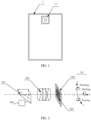
- FIG. 1 is a schematic structural diagram of a rear housing of a terminal according to a schematic embodiment of this application.
- a fixing slot 11 may be provided on the rear housing 1, and the fixing slot 11 is configured to fix the camera module.
- the periscope camera module is a camera module that can adjust a focal length through floating of a lens group inside the terminal, and can implement optical zooming without protruding from a terminal body in which the periscope camera module is located.
- the periscope camera module usually includes an optical folding element, a lens group, an image sensor, a housing, and a light incidence opening located on the housing. A structure of the periscope camera module has little impact on image quality, and can make the terminal lighter, thinner, and smaller.
- the periscope camera module does not need to protrude from the terminal body, a case in which a protruding part of the camera module is easily damaged due to an accident during photographing is avoided. Therefore, the periscope camera module may be applicable to a plurality of types of terminals.
- the camera module When the periscope camera module has an anti-jitter function, the camera module includes an optical folding element, an actuating structure, an inertial element, a lens group, and an image sensor that are sequentially arranged.
- the optical folding element is connected to the actuating structure.
- the inertial element detects a jitter
- the optical folding element may perform jitter compensation on an imaging light beam under driving of the actuating structure.
- movement precision of the optical folding element is limited, resulting in relatively low precision of final jitter compensation on the imaging light beam.
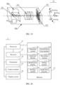
- FIG. 2 is a schematic structural diagram of a camera module 10 according to an embodiment of this application.
- the camera module 10 includes an optical folding element 101, a lens group 102, and an image sensor 103 that are sequentially arranged along a transmission direction of an imaging light beam.
- the imaging light beam is a light beam formed by light rays that are incident to the camera module.
- the optical folding element 101 is configured to: fold an optical path of a received imaging light beam and transfer the optical path to the lens group 102.
- Optical path folding is also referred to as optical path turning, and refers to changing a transmission path of a light ray.
- the optical folding element 101 may be a reflection element such as a prism or a reflex mirror.
- the lens group 102 may include one or more lenses, and is configured to transmit the received imaging light beam to the image sensor 103.
- the lens group 102 may further perform processing, for example, processing such as aberration correction, or achromatism, on the received imaging light beam.
- the image sensor 103 has an image capture region, and the image sensor 103 is configured to capture the received imaging light beam in the image capture region (also referred to as a light sensing region or a light sensing surface).
- the image sensor is a device having an optical-to-electrical conversion function, and can convert an optical signal of the imaging light beam captured in the image capture region into an electrical signal in a corresponding proportional relationship with the optical signal.
- the image sensor may be a CCD image sensor including a charged coupled device (charged coupled device, CCD) or a CMOS image sensor including a complementary metal-oxide semiconductor (complementary metal oxide semiconductor, CMOS).
- the camera module 10 further includes a front-end anti-jitter component 104 and a back-end anti-jitter component 105.
- the front-end anti-jitter component 104 is connected to at least one of the optical folding element 101 and the lens group 102.
- FIG. 2 schematically shows a case in which the front-end anti-jitter component 104 is connected to the optical folding element 101.
- the back-end anti-jitter component 105 is connected to the image sensor 103, the front-end anti-jitter component 104 is configured to perform first jitter compensation on the imaging light beam, and the back-end anti-jitter component 105 is configured to perform second jitter compensation on the imaging light beam, that is, the front-end anti-jitter component 104 and the back-end anti-jitter component 105 perform jitter compensation on the imaging light beam twice.
- a front end and a back end are defined based on a position of an anti-jitter component, and the front-end anti-jitter component is closer to an entrance of the imaging light beam (that is, the foregoing light incidence opening) than the back-end anti-jitter component.
- Compensation precision of the second jitter compensation is greater than compensation precision of the first jitter compensation, where the compensation precision is used to reflect a proximity degree between a position of an imaging light beam and an ideal target position of jitter compensation after the anti-jitter component performs jitter compensation on the imaging light beam.
- the compensation precision may be represented by a distance difference between the position of the imaging light beam and the ideal target position of the jitter compensation after the anti-jitter component performs jitter compensation on the imaging light beam.
- precision of the second jitter compensation is greater than precision of the first jitter compensation.
- a level of the compensation precision of the second jitter compensation may be a sub-pixel level, and the compensation precision of the second jitter compensation may be 0.1 micrometer or 0.01 micrometer; and a level of the compensation precision of the first jitter compensation may be a pixel level, and the compensation precision of the first jitter compensation may be 1 micrometer.
- the front-end anti-jitter component and the back-end anti-jitter component may respectively perform the first jitter compensation and the second jitter compensation on the imaging light beam, and the first jitter compensation and the second jitter compensation cooperate with each other, so that compared with a conventional case in which jitter compensation is performed for only once, a limitation of movement precision of the optical folding element on the jitter compensation for the camera module is reduced, and precision of final jitter compensation on the imaging light beam is improved.
- FIG. 3 is a schematic structural diagram of a back-end anti-jitter component 105 according to an embodiment of this application.
- the back-end anti-jitter component 105 includes an image sensor actuating structure 1051 and a first jitter detection structure 1052.
- the image sensor actuating structure 1051 is fixedly connected to the image sensor 103.
- the first jitter detection structure 1052 has a light sensing region, and the light sensing region is a region used to capture an image, and may also be considered as an imaging region.
- the first jitter detection structure 1052 is disposed around the image capture region of the image sensor 103, and the first jitter detection structure 1052 is configured to: capture a received imaging light beam in the light sensing region of the first jitter detection structure 1052, and detect whether the imaging light beam captured in the light sensing region jitters.
- the image sensor actuating structure 1051 is configured to: after the first jitter detection structure 1052 detects that the imaging light beam captured in the light sensing region jitters, drive the image sensor 103 to move, to perform second jitter compensation on the imaging light beam.
- the first jitter detection structure has a light sensing region, and the image sensor has an image capture region. Therefore, both the first jitter detection structure and the image sensor are image capture devices.
- a higher frame rate of the image capture device indicates a higher image capture speed of the image capture device, and an image capture speed of the first jitter detection structure should be greater than an image capture speed of the image sensor.
- the first jitter detection structure may capture an image in the light sensing region before the image sensor does, to perform corresponding jitter compensation on an imaging light beam captured by the image sensor. Therefore, a frame rate of the first jitter detection structure is greater than a frame rate of the image sensor.
- the frame rate of the first jitter detection structure may be 10 times the frame rate of the image sensor.
- the camera module provided in this embodiment of this application has an internal coordinate system (also referred to as an internal reference coordinate system).
- the internal coordinate system is a stereoscopic coordinate system, and uses a center of an image sensor as an origin.
- the internal coordinate system includes: a z axis parallel to an optical axis L of a lens group, an x axis perpendicular to the z axis and parallel to a height direction of the lens group, and a y axis perpendicular to the z axis and perpendicular to the height direction of the lens group.
- Rotating around the z axis is referred to as rolling (roll), and is also referred to as moving around a roll axis.
- Rotating around the x axis is referred to as pitching (pitch), and is also referred to as moving around a pitch axis.
- Rotating around the y axis is referred to as yawing (yaw), and is also referred to as moving around a yaw axis.
- an anti-jitter component controls, based on a jitter direction of an imaging light beam received by an optical device connected to the anti-jitter component (for example, for a front-end anti-jitter component, the optical device is an optical folding element and/or a lens group; and for a back-end anti-jitter component, the optical device is an image sensor), the optical device to move along a jitter direction, to compensate for a jitter of the imaging light beam in the jitter direction.
- an optical device connected to the anti-jitter component for example, for a front-end anti-jitter component, the optical device is an optical folding element and/or a lens group; and for a back-end anti-jitter component, the optical device is an image sensor
- an anti-jitter component connected to the optical device controls the optical device to move along the positive direction of the x axis.
- the jitter direction of the imaging light beam received by the optical device is a clockwise direction of the yaw axis
- the anti-jitter component connected to the optical device can control the optical device to move along the positive direction of the x axis, to perform equivalent compensation for the jitter.
- the anti-jitter component can control the optical device to move along a negative direction of the y axis, to perform equivalent compensation for the jitter.
- the anti-jitter component can control the optical device to move along a positive direction of the y axis, to perform equivalent compensation for the jitter.
- the anti-jitter component can control the optical device to move along the negative direction of the y axis, to perform equivalent compensation for the jitter.
- the image sensor actuating structure 1051 may drive the image sensor 103 to move in a plurality of directions.
- the direction may be an x-axis direction, a y-axis direction, or a yaw-axis direction of the internal coordinate system of the camera module.
- the image sensor actuating structure 1051 may be implemented by using a micro-electro-mechanical systems (Micro-Electro-Mechanical Systems, MEMS) actuator technology, may be implemented by using a voice coil motor (voice coil motor, VCM) technology, or may be implemented by using a shape memory alloy (shape memory alloy, SMA) motor technology.
- MEMS micro-electro-mechanical systems
- VCM voice coil motor
- SMA shape memory alloy
- Movement precision of the MEMS executor is higher than movement precision of the VCM and the SMA motor. Therefore, when the image sensor actuating structure is the MEMS executor, the MEMS executor can control the image sensor to move, to perform jitter compensation with relatively high precision on the imaging light beam.
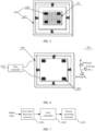
- FIG. 4 is a schematic diagram of an image sensor actuating structure according to an embodiment of this application.
- the image sensor actuating structure 1051 includes a movable carrying platform 10511, a base 10512, an elastic suspension element 10513, and an actuating member (not shown in the figure).
- the base 10512 is fixedly disposed.
- the base 10512 may be fixedly disposed on the housing, or the base may be fixedly disposed on a structure (for example, a median plate) of a terminal in which the base is located.
- the movable carrying platform 10511 is connected to the base 10512 by using the elastic suspension element 10513, and the movable carrying platform 10511 is fixedly connected to the actuating member.
- the elastic suspension element 10513 may be a cantilever beam structure having elasticity, or the like.
- the movable carrying platform 10511 is configured to carry the image sensor 103 and the first jitter detection structure 1052.
- the actuating member is configured to drive the movable carrying platform 10511 to move relative to the base 10512.
- the base 10512 is a housing having a groove
- the movable carrying platform 10511 is of a rectangular plate structure and is disposed in the groove
- at least two first positions on a side wall of the movable carrying platform 10511 are respectively connected to at least two second positions on an inner wall of the groove through the elastic suspension element 10513 in a one-to-one correspondence
- the second position that is on the inner wall and that corresponds to each first position on the side wall is a position that is on the inner wall of the groove and that is closest to the side wall.
- the at least two first positions are usually evenly distributed on the side wall, to ensure that the movable carrying platform is evenly subjected to a force.
- an opening of the groove is in a rectangular, circular, or another shape.
- the opening of the groove is in a rectangular shape
- at least two side walls of the movable carrying platform 10511 are respectively connected to at least two inner walls of the groove in a one-to-one correspondence through the elastic suspension element 10513
- the inner wall corresponding to each side wall is an inner wall that is in inner walls of the groove and that is closest to the side wall, and there may be one or more elastic suspension elements between each side wall and the corresponding inner wall.
- the actuating member is configured to drive the movable carrying platform 10511 to perform, in the groove, at least one action of rotating around an optical axis of a lens group (that is, performing an angular displacement) and translating along a direction perpendicular to the optical axis of the lens group (that is, performing a straight line displacement).
- rotating around the optical axis of the lens group refers to rotating around a z axis of an internal coordinate system, that is, moving around a roll axis.
- Translating along the direction perpendicular to the optical axis of the lens group is translating along an x axis or a y axis of the internal coordinate system.
- the activating member may be an electrostatic activating member, an electromagnetic activating member, an electrothermal activating member, a piezoelectric activating member, or the like.
- the activating member may drive, by adjusting a loaded electrostatic force, the movable carrying platform to move in the groove.
- the activating member is an electromagnetic activating member, the activating member may drive, by adjusting a magnetic property to be positive or negative, the movable carrying platform to move in the groove.
- the activating member is an electrothermal activating member
- the activating member may control and drive, by adjusting a temperature, the movable carrying platform to perform a movement action in the groove.
- the actuating member is a piezoelectric actuating member
- the actuating member may drive, by adjusting strength of an external electric field, the movable carrying platform to move in the groove.
- the first jitter detection structure 1052 may be fixedly connected to the movable carrying platform.
- the first jitter detection structure 1052 may also be integrated in a region outside an image capture region of the image sensor 103.
- the first jitter detection structure does not need to be separately installed, and an overall installation process of the camera module may be simplified.
- a part of the first jitter detection structure 1052 is fixedly connected to the movable carrying platform, and the other part is integrated in a region outside the image capture region of the image sensor 103.
- the first jitter detection structure includes at least one image shake sensor.
- the image shake sensor may be a high frame rate image sensor (that is, a frame rate of the image shake sensor is greater than a specified frame rate).
- the first jitter detection structure may include four image shake sensors.
- all the image shake sensors have a same frame rate greater than the frame rate of the image sensor. In this way, when an imaging light beam is transmitted from the lens group to the back-end anti-jitter component, the image shake sensor may perform accurate image capturing in the light sensing region before the image sensor does, so that a jitter direction and a jitter amount of a captured image can be predicted, and further, jitter compensation is performed.
- the tracking error is a distance difference between a position of the imaging light beam and an ideal target position of first jitter compensation after the anti-jitter component performs jitter compensation on the imaging light beam.
- an area of the light sensing region may be greater than or equal to a square of a maximum tracking error of the front-end anti-jitter component.
- the sensed jitter amount of the imaging light beam is within a range that can be sensed by the image shake sensor
- the maximum tracking error is a maximum difference between an offset distance of a position of the imaging light beam and an offset distance of an ideal target position of the first jitter compensation after the front-end anti-jitter component performs the first jitter compensation on the imaging light beam.
- the maximum tracking error is obtained in advance through experiment or through simulation by using simulation software.
- the light sensing region of the image shake sensor may have a pixel density greater than or equal to a pixel density of the image capture region of the image sensor. Therefore, the image shake sensor is enabled to perform clearer imaging on the received imaging light beam, that is, precision of imaging the received imaging light beam by the image shake sensor is higher than precision of imaging the received imaging light beam by the image sensor, to further improve the precision of sensing the jitter amount of the image.
- the back-end anti-jitter component 105 further includes a first controller 1053.
- the first controller 1053 is separately connected to a first jitter detection structure 1052 and an image sensor actuating structure 1051.
- the first controller 1053 is configured to perform a second jitter compensation control process, that is, obtain a first jitter direction and a first jitter amount of an imaging light beam that are detected by a first jitter detection structure 1052, determine a first jitter compensation direction and a first jitter compensation displacement based on the first jitter direction and the first jitter amount, and control, based on the first jitter compensation direction and the first jitter compensation displacement, the image sensor actuating structure 1051 to drive the image sensor 103 to move the first jitter compensation displacement along the first jitter compensation direction.
- a second jitter compensation control process that is, obtain a first jitter direction and a first jitter amount of an imaging light beam that are detected by a first jitter detection structure 1052, determine a first jitter compensation direction and a first jitter compensation displacement based on the first jitter direction and the first jitter amount, and control, based on the first jitter compensation direction and the first jitter compensation
- FIG. 7 is a schematic diagram of control logic in a second jitter compensation process performed by the back-end anti-jitter component shown in FIG. 6 .
- a first jitter detection structure 1052 detects, by using an imaging light beam captured in a light sensing region, a first jitter direction and a first jitter amount of the imaging light beam.
- the first controller 1053 obtains the first jitter direction and the first jitter amount that are detected by the first jitter detection structure 1052, determines a first jitter compensation direction and a first jitter compensation displacement based on the first jitter direction and the first jitter amount, and further controls the image sensor actuating structure 1051 to drive the image sensor to move the first jitter compensation displacement along the first jitter compensation direction.
- the first jitter compensation direction may include at least one direction in the foregoing internal coordinate system, the first jitter compensation displacement includes a compensation displacement in a one-to-one correspondence with the at least one direction, and the compensation displacement may be a straight line displacement or an angular displacement.
- the first jitter compensation direction may include the x-axis direction and the roll-axis direction of the internal coordinate system.
- the first jitter compensation displacement includes a straight line displacement of m (0 ⁇ m ⁇ 1) micrometer in the x-axis direction and an angular displacement of n (0 ⁇ n ⁇ 1) degrees in the roll-axis direction.
- the back-end anti-jitter component 105 further includes: a displacement sensor 1054, where the displacement sensor 1054 is fixedly connected to an image sensor (not shown in the figure), or is fixedly connected to a specified position in an image sensor actuating structure 1051, and the specified position is a position of a device that is in the image sensor actuating structure 1051 and that synchronously moves with the image sensor.
- the image sensor actuating structure is a structure shown in FIG. 8
- the specified position is a position of a movable carrying platform of the image sensor actuating structure, that is, the displacement sensor is fixedly connected to the movable carrying platform of the image sensor actuating structure.
- the displacement sensor 1054 is configured to send, to the first controller 1053 in a process in which the image sensor actuating structure 1051 drives the image sensor to move, a feedback signal indicating a current displacement of the displacement sensor.
- the displacement sensor 1054 includes at least one of a linear displacement sensor and an angular displacement sensor.
- the linear displacement sensor is configured to send, to the first controller in a process in which the image sensor actuating structure drives the image sensor to move, a feedback signal indicating a current linear displacement.
- the angular displacement sensor is configured to send, to the first controller in a process in which the image sensor actuating structure drives the image sensor to move, a feedback signal indicating a current angular displacement.
- the first controller 1053 is configured to control, based on the feedback signal, the image sensor actuating structure 1051 to drive the image sensor to re-perform jitter compensation.
- the first controller 1053 may determine a displacement of the image sensor based on the feedback signal, and when the displacement of the image sensor is different from a first jitter compensation displacement, control the image sensor actuating structure 1051 to drive the image sensor to re-perform jitter compensation, that is, send a control signal to the image sensor actuating structure 1051, to instruct the image sensor actuating structure 1051 to drive the image sensor to move a first displacement along the first jitter compensation direction, where the first displacement is a difference between the first jitter compensation displacement and the displacement of the image sensor.
- the first displacement is a positive value
- an absolute value of the first displacement is moved along the first jitter compensation direction
- the absolute value of the first displacement is moved in a reverse direction of the first jitter compensation direction.
- the first controller 1053 may send a control signal to the image sensor actuating structure 1051, to instruct the image sensor actuating structure 1051 to drive the image sensor to move a second displacement along the first jitter compensation direction, where the second displacement is 0.
- a jitter process is a continuous process
- the foregoing second jitter compensation control process is continuously and repeatedly performed, and the foregoing control process of re-performed jitter compensation is also continuously and repeatedly performed. In this way, a position of the image sensor can be adjusted in real time, thereby ensuring final compensation precision.
- the first controller forms closed-loop feedback control on the image sensor actuating structure by using the displacement sensor, that is, a feedback mechanism for a current displacement of the image sensor actuating structure is established by using the displacement sensor, thereby improving precise control of the first controller on the current displacement of the image sensor actuating structure, and improving compensation precision of the back-end anti-jitter component.
- FIG. 9 is a schematic diagram of control logic in a second jitter compensation process performed by the back-end anti-jitter component shown in FIG. 8 .
- a first controller 1053 controls an image sensor actuating structure 1051 to drive an image sensor to move a first jitter compensation displacement along a first jitter compensation direction
- a working process of a displacement sensor 1054 shown in FIG. 9 may be as follows:
- the displacement sensor 1054 sends, to the first controller 1053 in real time, a feedback signal indicating a current displacement of the displacement sensor, and the first controller 1053 determines the displacement of the image sensor based on the feedback signal.
- the first controller 1053 controls the image sensor actuating structure 1051 to drive the image sensor to re-perform jitter compensation, that is, sends a control signal to the image sensor actuating structure 1051, to instruct the image sensor actuating structure 1051 to drive the image sensor to move the first displacement along the first jitter compensation direction.
- the first controller 1053 may send a control signal to the image sensor actuating structure 1051, to instruct the image sensor actuating structure 1051 to drive the image sensor to move a second displacement along the first jitter compensation direction, where the second displacement is 0.
- the displacement sensor 1054 may obtain the first jitter compensation displacement.
- the displacement sensor 1054 sends, to the first controller 1053, a feedback signal indicating the first jitter compensation displacement.
- the first controller 1053 determines the displacement of the image sensor, and continues to execute the control logic in the foregoing second jitter compensation process performed by the back-end anti-jitter component shown in FIG. 7 .
- the first controller 1053 may send a control signal to the image sensor actuating structure 1051, to instruct the image sensor actuating structure 1051 to drive the image sensor to move a second displacement along the first jitter compensation direction, where the second displacement is 0.
- the first controller controls the image sensor to perform a multi-dimensional movement by controlling the image sensor actuating structure to perform a multi-dimensional movement, to implement the second jitter compensation performed on the imaging light beam.
- the second jitter compensation process includes: As shown in FIG. 8 , when a jitter direction of the imaging light beam is the yaw-axis direction, the first controller controls the image sensor actuating structure to drive the image sensor to move along the x-axis direction. When a jitter direction of the imaging light beam is the x-axis direction, the image sensor actuating structure moves along the x-axis direction.
- the image sensor actuating structure moves along the y-axis direction.
- the image sensor actuating structure moves along the y-axis direction.
- the image sensor actuating structure drives the image sensor to move around the roll-axis direction.
- the back-end anti-jitter component includes an image shake sensor, a first controller, a MEMS executor, and a displacement sensor.
- the displacement sensor is separately disposed in the back-end anti-jitter component.
- the control logic in the jitter compensation process performed by the back-end anti-jitter component is as follows:
- the image shake sensor detects, by using an imaging light beam captured in a light sensing region, a first jitter direction and a first jitter amount of the imaging light beam.
- the first controller performs a second jitter compensation control process, and the first controller obtains the first jitter direction and the first jitter amount that are detected by the image shake sensor, determines a first jitter compensation direction and a first jitter compensation displacement based on the first jitter direction and the first jitter amount, and further controls the MEMS actuator to drive the image sensor to move the first jitter compensation displacement along the first jitter compensation direction.
- the displacement sensor sends, to the first controller in real time, a feedback signal indicating a current displacement of the displacement sensor, and the first controller determines the displacement of the image sensor based on the feedback signal.
- the first controller controls the MEMS actuator to drive the image sensor to re-perform jitter compensation, that is, sends a control signal to the MEMS actuator, to instruct the MEMS actuator to drive the image sensor to move a first displacement along the first jitter compensation direction.
- the second jitter compensation control process performed by the first controller continues to be performed.
- the first controller may send a control signal to the MEMS executor, to instruct the MEMS executor to drive the image sensor to move a second displacement along the first jitter compensation direction, where the second displacement is 0, so that the first controller adjusts a position of the image sensor in real time.
- the displacement sensor may be integrated into the MEMS actuator.
- control logic in the second jitter compensation process performed by the back-end anti-jitter component refer to the control logic in the second jitter compensation process performed by the back-end anti-jitter component in the first optional implementation.
- the control logic in the second jitter compensation process performed by the back-end anti-jitter component is not limited in this embodiment of this application.
- the displacement sensor is a linear displacement sensor
- the image shake sensor detects a straight line displacement that has a length of w micrometers and that is of an imaging light beam in the positive direction of the x axis.
- the first controller obtains the direction and the length of the straight line displacement of the imaging light beam that are detected by the image shake sensor, determines, based on the detection of the image shake sensor, that the first jitter compensation direction is the positive direction of the x axis and the first jitter compensation displacement is a straight line displacement having a length of u micrometers in the positive direction of the x axis, and further controls the MEMS actuator to drive the image sensor to move u micrometers along the positive direction of the x axis.
- the linear displacement sensor sends, to the first controller in real time, a feedback signal indicating a current displacement of the displacement sensor, and the first controller determines, based on the feedback signal, that the image sensor moves q micrometers along the positive direction of the x axis, and when q#u, controls the MEMS actuator to drive the image sensor to re-perform jitter compensation, that is, sends a control signal to the MEMS actuator, to instruct the MEMS actuator to drive the image sensor to move p micrometers along the positive direction of the x axis.
- the MEMS actuator drives the image sensor to move
- the second jitter compensation control process performed by the first controller continues to be performed.
- the first controller may send a control signal to the MEMS actuator, to instruct the MEMS actuator to drive the image sensor to move 0 micrometers along the positive direction of the x axis, so that the first controller adjusts a position of the image sensor in real time.
- Numerical precision of w, u, q and p may each be 0.1, 0.01, or 0.001.
- the MEMS actuator may be a translational in-plane MEMS actuator.
- the translational in-plane MEMS actuator means that the MEMS actuator drives only a device connected to the MEMS actuator (namely, the image sensor) to move in a plane.
- the MEMS actuator may drive the device connected to the MEMS actuator to perform a straight line movement and/or moves around the roll axis in the x-axis direction and the y-axis direction.
- the image shake sensor may directly detect a jitter direction and a jitter amount of an image, where the jitter amount and the jitter direction are more precise compared with a jitter direction and a jitter amount of the camera module that are detected by an inertial element. Therefore, jitter compensation triggered based on the image shake sensor is more precise.
- the camera module further includes the front-end anti-jitter component, where the front-end anti-jitter component may be disposed in a plurality of positions, to perform first jitter compensation on an imaging light beam.
- the front-end anti-jitter component is disposed in the following three positions is used for description.
- the front-end anti-jitter component 104 may be connected to an optical folding element 101, and the front-end anti-jitter component 104 includes a folding element actuating structure 1041 and a second jitter detection structure 1042.
- the folding element actuating structure 1041 is fixedly connected to the optical folding element 101, and the second jitter detection structure 1042 is fixedly disposed.
- the second jitter detection structure 1042 may be fixedly disposed on the housing.
- the second jitter detection structure 1042 may be fixedly disposed on a structure (for example, a median plate) of a terminal in which the second jitter detection structure 1042 is located.
- the second jitter detection structure 1042 is configured to detect whether the camera module jitters.
- the second jitter detection structure 1042 may be an inertial element such as a gyroscope or an accelerometer.
- the folding element actuating structure 1041 is configured to: after the second jitter detection structure 1042 detects that the camera module 10 jitters, drive the optical folding element 101 to move, to perform first jitter compensation on the imaging light beam.
- the folding element actuating structure 1041 may drive the optical folding element 101 to move in a plurality of directions.
- the direction may be a direction of a pitch axis and a direction of a yaw axis that are in an internal coordinate system of the camera module.
- the folding element actuating structure 1041 may be implemented by using a MEMS actuator technology, or may be implemented by using a VCM technology, or may be implemented by using an SMA motor technology.
- the front-end anti-jitter component 104 further includes a third controller 1043, where the third controller 1043 is separately connected to the second jitter detection structure 1042 and the folding element actuating structure 1041.
- the third controller 1043 is configured to perform a first jitter compensation control process, that is, obtain a third jitter direction and a third jitter amount of the camera module 10 that are detected by the second jitter detection structure 1042, determine a third jitter compensation direction and a third jitter compensation displacement based on the third jitter direction and the third jitter amount, and control, based on the third jitter compensation direction and the third jitter compensation displacement, the folding element actuating structure 1041 to drive the optical folding element 101 to move the third jitter compensation displacement along the third jitter compensation direction.
- a first jitter compensation control process that is, obtain a third jitter direction and a third jitter amount of the camera module 10 that are detected by the second jitter detection structure 1042, determine a third jitter compensation direction and a third jitter compensation displacement based on the third jitter direction and the third jitter amount, and control, based on the third jitter compensation direction and the third jitter compensation displacement,
- FIG. 11 is a schematic diagram of control logic in a jitter compensation process performed by the camera module shown in FIG. 10 . That is, FIG. 11 is a schematic diagram of control logic in a jitter compensation process performed on an imaging light beam by a front-end anti-jitter component in cooperation with a back-end anti-jitter component.
- the second jitter detection structure 1042 detects a third jitter direction and a third jitter amount of the camera module.
- the third controller 1043 obtains the third jitter direction and the third jitter amount that are detected by the second jitter detection structure 1042, determines a third jitter compensation direction and a third jitter compensation displacement based on the third jitter direction and the third jitter amount, and further controls the folding element actuating structure 1041 to drive the optical folding element to move the third jitter compensation displacement along the third jitter compensation direction, to complete first jitter compensation performed by the front-end anti-jitter component on the imaging light beam. Afterwards, the back-end anti-jitter component performs second jitter compensation on the imaging light beam after the first jitter compensation performed by the front-end anti-jitter component.
- the third jitter compensation direction may include at least one direction in the foregoing internal coordinate system, and the third jitter compensation displacement includes a compensation displacement in a one-to-one correspondence with the at least one direction, where the compensation displacement may be a straight line displacement or an angular displacement.
- the front-end anti-jitter component further includes a first feedback sensor, and the first feedback sensor is fixedly connected to the optical folding element or the folding element actuating structure.
- the first feedback sensor may be a Hall effect sensor, or may be a displacement sensor.
- the first feedback sensor is configured to: in a process in which the folding element actuating structure drives the optical folding element to move, send, to the third controller, a feedback signal indicating a current displacement of the first feedback sensor.
- the third controller is configured to control, based on the feedback signal, the folding element actuating structure to drive the optical folding element to re-perform jitter compensation.
- the third controller may determine a displacement of the optical folding element based on the feedback signal, and when the displacement of the optical folding element is different from the third jitter compensation displacement, control the folding element actuating structure to drive the optical folding element to re-perform jitter compensation, that is, send a control signal to the folding element actuating structure, to instruct the folding element actuating structure to drive the optical folding element to move the third displacement along the third jitter compensation direction, where the third displacement is a difference between the third jitter compensation displacement and the displacement of the optical folding element.
- the third displacement is a positive value
- an absolute value of the third displacement is moved along the third jitter compensation direction
- the third displacement is a negative value
- the absolute value of the third displacement is moved along a reverse direction of the third jitter compensation direction.
- the third controller may send a control signal to the folding element actuating structure, to instruct the folding element actuating structure to drive the optical folding element to move a fourth displacement along the third jitter compensation direction, where the fourth displacement is 0.
- a jitter process is a continuous process
- the foregoing first jitter compensation control process is continuously and repeatedly performed, and the foregoing control process of re-performed jitter compensation is also continuously and repeatedly performed. In this way, a position of the optical folding element can be adjusted in real time, thereby ensuring final compensation precision.
- the third controller forms closed-loop feedback control on the folding element actuating structure by using the feedback sensor, that is, a feedback mechanism for a current displacement of the folding element actuating structure is established by using the feedback sensor, thereby improving precise control of the third controller on the current displacement of the folding element actuating structure, and improving compensation precision of the front-end anti-jitter component.
- the first feedback sensor may be integrated on the folding element actuating structure.
- FIG. 12 is a schematic diagram of control logic in a jitter compensation process performed by the camera module shown in FIG. 10 when the camera module includes a first feedback sensor.
- the third controller 1043 controls the folding element actuating structure 1041 to drive the optical folding element to move the third jitter compensation displacement along the third jitter compensation direction, refer to FIG. 11 .
- the working process of the first feedback sensor refer to the working process of the displacement sensor shown in FIG. 9 . Details are not described in this embodiment of this application.
- the front-end anti-jitter component completes the first jitter compensation performed on the imaging light beam
- the back-end anti-jitter component performs the second jitter compensation on the imaging light beam after the first jitter compensation performed by the front-end anti-jitter component.
- control logic in the jitter compensation process performed by the camera module includes:
- the gyroscope detects the third jitter direction and the third jitter amount of the camera module.
- the third controller obtains the third jitter direction and the third jitter amount that are detected by the gyroscope, determines the third jitter compensation direction and the third jitter compensation displacement based on the third jitter direction and the third jitter amount, and further, controls the VCM to drive the optical folding element to move the third jitter compensation displacement along the third jitter compensation direction.
- the Hall effect sensor sends, to the third controller in real time, a feedback signal indicating a current displacement of the Hall effect sensor.
- the third controller determines the displacement of the optical folding element based on the feedback signal, and when the displacement of the optical folding element is different from the third jitter compensation displacement, controls the folding element actuating structure to drive the optical folding element to re-perform jitter compensation, that is, sends a control signal to the folding element actuating structure, to instruct the folding element actuating structure to drive the optical folding element to move the third displacement along the third jitter compensation direction.
- the first jitter compensation control process continues to be performed.
- the third controller may send a control signal to the folding element actuating structure, to instruct the folding element actuating structure to drive the optical folding element to move a fourth displacement long the third jitter compensation direction, where the fourth displacement is 0.
- the back-end anti-jitter component performs the second jitter compensation on the imaging light beam after the first jitter compensation performed by the front-end anti-jitter component.
- the third controller controls the optical folding element to perform a multi-dimensional movement by controlling the folding element actuating structure to perform a multi-dimensional movement, to implement the first jitter compensation performed on the imaging light beam.
- a process of the first jitter compensation includes: As shown in FIG. 10 , when a jitter direction of the imaging light beam is a yaw-axis and/or x-axis direction, the third controller controls the folding element actuating structure to drive the optical folding element to move along the yaw-axis direction. When a jitter direction of the imaging light beam is a pitch-axis and/or y-axis direction, the image sensor actuating structure moves along the pitch-axis direction.
- a front-end anti-jitter component 104 may be connected to a lens group 102, and the front-end anti-jitter component 104 includes a lens group actuating structure 1044 and a third jitter detection structure 1045.
- the lens group actuating structure 1044 is fixedly connected to the lens group 102.
- the third jitter detection structure 1045 is fixedly disposed.
- the camera module includes a housing
- the third jitter detection structure 1045 may be fixedly disposed on the housing, or the third jitter detection structure 1045 may be fixedly disposed on a structure (for example, a median plate) of a terminal in which the third jitter detection structure 1045 is located.
- the lens group actuating structure 1044 is configured to: after the third jitter detection structure 1045 detects a jitter of a camera module 10, drive the lens group 102 to move, to perform jitter compensation on an imaging light beam.
- the lens group actuating structure 1044 may drive the lens group 102 to move in a plurality of directions.
- the direction may be an x-axis direction, a y-axis direction, a pitch-axis direction, a yaw-axis direction in an internal coordinate system of the camera module.
- the third jitter detection structure 1045 may be an inertial element such as a gyroscope or an accelerometer.
- the lens group actuating structure 1044 may be implemented by using a MEMS actuator technology, or may be implemented by using a VCM technology, or may be implemented by using an SMA motor technology.
- the front-end anti-jitter component 104 further includes a fourth controller 1046, where the fourth controller 1046 is separately connected to the third jitter detection structure 1045 and the lens group actuating structure 1044.
- the fourth controller 1046 is configured to perform a first jitter compensation control process, that is, obtain a fourth jitter direction and a fourth jitter amount of the camera module that are detected by the third jitter detection structure 1045, determine a fourth jitter compensation direction and a fourth jitter compensation displacement based on the fourth jitter direction and the fourth jitter amount, and control, based on the fourth jitter compensation direction and the fourth jitter compensation displacement, the lens group actuating structure 1044 to drive the lens group 102 to move the fourth jitter compensation displacement along the fourth jitter compensation direction.
- a first jitter compensation control process that is, obtain a fourth jitter direction and a fourth jitter amount of the camera module that are detected by the third jitter detection structure 1045, determine a fourth jitter compensation direction and a fourth jitter compensation displacement based on the fourth jitter direction and the fourth jitter amount, and control, based on the fourth jitter compensation direction and the fourth jitter compensation displacement, the lens
- FIG. 14 is a schematic diagram of control logic in a jitter compensation process performed by the camera module shown in FIG. 13 .
- a process in which the fourth controller 1046 controls the lens group actuating structure 1044 to drive the lens group to move the fourth jitter compensation displacement along the fourth jitter compensation direction is basically the same as a process in which the third controller controls the folding element actuating structure to drive the optical folding element to move the third jitter compensation displacement along the third jitter compensation direction. Therefore, the control logic in the jitter compensation process performed by the camera module is the same as the control logic in the jitter compensation process performed by the camera module shown in FIG. 10 in the foregoing first implementable manner. Details are not described in this embodiment of this application.
- the front-end anti-jitter component further includes a second feedback sensor, and the second feedback sensor is fixedly connected to the lens group or the lens group actuating structure.
- the second feedback sensor may be a Hall effect sensor, or may be a displacement sensor.
- a function of the second feedback sensor is basically the same as that of the first feedback sensor, and the second feedback sensor is configured to send a feedback signal of a current displacement of the lens group to the fourth controller.
- a function of the fourth controller is basically the same as that of the third controller.
- FIG. 15 is a schematic diagram of control logic in a jitter compensation process performed by the camera module shown in FIG. 13 when the camera module includes a second feedback sensor.
- the control logic in the jitter compensation process performed by the camera module is the same as the control logic in the jitter compensation process performed by the camera module shown in FIG. 10 when the camera module includes the first feedback sensor in the foregoing first implementable manner. Details are not described again in this embodiment of this application.
- the third jitter detection structure is a gyroscope
- the second feedback sensor is a Hall effect sensor
- the lens group actuating structure is a VCM.
- a process in which the fourth controller controls the VCM to drive the lens group to move the fourth jitter compensation displacement along the fourth jitter compensation direction is basically the same as a process in which the third controller controls the VCM to drive the optical folding element to move the third jitter compensation displacement along the third jitter compensation direction. Therefore, control logic in the jitter compensation process performed by the camera module is basically the same as the control logic mentioned in the example corresponding to the schematic diagram of the control logic shown in FIG. 12 . Details are not described again in this embodiment of this application.
- the fourth controller controls the lens group to perform a multi-dimensional movement by controlling the lens group actuating structure to perform a multi-dimensional movement, to implement the first jitter compensation performed on the imaging light beam.
- the first jitter compensation process includes: As shown in FIG. 13 , when a jitter direction of an imaging light beam is a yaw-axis direction, the third controller controls the folding element actuating structure to drive the optical folding element to move along the yaw-axis direction. When a jitter direction of the imaging light beam is an x-axis direction, the third controller controls the folding element actuating structure to drive the optical folding element to move along the x-axis direction.
- the image sensor actuating structure moves along the pitch-axis direction.
- the image sensor actuating structure moves along the y-axis direction.
- a front-end anti-jitter component 104 may be connected to both an optical folding element 101 and a lens group 102.
- the front-end anti-jitter component 104 includes all structures in the first optional implementation and the second optional implementation, that is, the front-end anti-jitter component 104 includes: a folding element actuating structure 1041, a second jitter detection structure 1042, a third controller 1043, a lens group actuating structure 1044, a third jitter detection structure 1045, and a fourth controller 1046.
- FIG. 17 is a schematic diagram of control logic in a jitter compensation process performed by the camera module shown in FIG. 16 .
- the third controller 1043 controls the folding element actuating structure 1041 to drive the optical folding element to move a third jitter compensation displacement along a third jitter compensation direction
- the fourth controller 1046 controls the lens group actuating structure 1044 to drive the lens group to move a fourth jitter compensation displacement along a fourth jitter compensation direction
- FIG. 14 Details are not described again in this embodiment of this application.
- the back-end anti-jitter component After the front-end anti-jitter component completes first jitter compensation performed on the imaging light beam, the back-end anti-jitter component performs second jitter compensation on the imaging light beam after the first jitter compensation performed by the front-end anti-jitter component.
- the front-end anti-jitter component further includes a first feedback sensor and a second feedback sensor.
- first feedback sensor and the front-end anti-jitter component For connection relationships between the first feedback sensor and the front-end anti-jitter component and between the second feedback sensor and the front-end anti-jitter component, refer to those in the first and second optional implementations.
- FIG. 18 is a schematic diagram of control logic in a jitter compensation process performed by the camera module shown in FIG. 16 when the camera module includes a first feedback sensor and a second feedback sensor.
- the third controller 1043 controls the folding element actuating structure 1041 to drive the optical folding element to move a third jitter compensation displacement along a third jitter compensation direction
- the fourth controller 1046 controls the lens group actuating structure 1044 to drive the lens group to move a fourth jitter compensation displacement along a fourth jitter compensation direction
- FIG. 15 Details are not described again in this embodiment of this application.
- the back-end anti-jitter component After the front-end anti-jitter component completes first jitter compensation performed on the imaging light beam, the back-end anti-jitter component performs second jitter compensation on the imaging light beam after the first jitter compensation performed by the front-end anti-jitter component.
- both the second jitter detection structure and the third jitter detection structure are gyroscopes
- both the first feedback sensor and the second feedback sensor are Hall effect sensors
- both the folding element actuating structure and the lens group actuating structure are VCMs.
- the control logic in the jitter compensation process performed by the camera module includes: a process in which the third controller controls the VCM to drive the optical folding element to move the third jitter compensation displacement along the third jitter compensation direction in the example corresponding to the schematic diagram of the control logic shown in FIG.
- the third controller and the fourth controller may be one controller. It is assumed that the controller may be a second controller, and the second controller is separately connected to the second jitter detection structure, the third jitter detection structure, the image sensor actuating structure, the lens group actuating structure, and the folding element actuating structure.
- the second controller is configured to: receive a second jitter direction and a second jitter amount of the camera module that are detected by the second jitter detection structure and the third jitter detection structure, determine a target jitter direction and a target jitter amount based on the second jitter direction and the second jitter amount, and separately control the lens group actuating structure and the folding element actuating structure to move, so that a total displacement of movements of the lens group and the optical folding element in the target jitter direction is the target jitter amount.
- control logic in the jitter compensation process performed by the camera module is basically the same as the control logic in the jitter compensation process performed by the camera module shown in FIG. 18 .
- the second controller simultaneously obtains the second jitter direction and the second jitter amount that are detected by the second jitter detection structure and the third jitter detection structure, and allocates the second jitter direction and the second jitter amount, so that the optical folding element and the lens group move in the target jitter direction separately.
- the total displacement of the movement is the target jitter amount. Details are not described in this embodiment of this application.
- optical folding element may alternatively be integrated into the folding element actuating structure
- the lens group may alternatively be integrated into the lens group actuating structure
- the image sensor may alternatively be integrated into the image sensor actuating structure.
- the camera module 10 further includes a housing 106 having a cavity, and an optical folding element 101, a lens group 102, an image sensor 103, a front-end anti-jitter component 104, and a back-end anti-jitter component 105 are fixedly disposed in the housing 106, one end of the housing 106 is provided with a light incidence opening 1061, and the light incidence opening 1061 is for incidence of an imaging light beam.
- FIG. 19 is a schematic structural diagram of the camera module when the front-end anti-jitter component 104 is connected to the optical folding element 101.
- the front-end anti-jitter component and the back-end anti-jitter component may respectively perform the first jitter compensation and the second jitter compensation on the imaging light beam, and the first jitter compensation and the second jitter compensation cooperate with each other, so that compared with a conventional case in which jitter compensation is performed for only once, precision of final jitter compensation on the imaging light beam is improved.
- first jitter compensation and the second jitter compensation cooperate with each other, a jitter compensation range for a long-focus optical path is expanded.
- precision of the second jitter compensation is greater than precision of the first jitter compensation, precision of jitter compensation for the long-focus optical path is improved.
- the front-end anti-jitter component may implement four-axis (x, y, pitch, and yaw axes) jitter compensation
- the back-end anti-jitter component may not only cooperate with the image sensor actuating structure having relatively high precision by using a first jitter detection structure having relatively high precision, to implement the four axes (x, y, pitch, and yaw axes) jitter compensation with relatively high precision, but also implement jitter compensation on an imaging light beam in a jitter direction of a roll axis by using an angular displacement of the image sensor in the direction of the roll axis, so that the camera module implements a five-axis anti-jitter function.
- FIG. 20 is a schematic structural diagram of a terminal according to an embodiment of this application.
- the terminal 2 includes a processor 21, a memory 22, a data transmission component, and at least one camera module 25.
- the data transmission component may be a receiver 23 and a transmitter 24.
- the at least one camera module 25 includes any camera module provided in the embodiments of this application.
- the terminal may be a mobile phone, a notebook computer, a tablet, an event data recorder, a camera, a monitoring device, or the like.
- the mobile phone when the terminal is a mobile phone, the mobile phone includes a front-facing camera module and a rear-facing camera module, and the rear-facing camera module is any camera module provided in the embodiments of this application.
- the processor 21 may be a control center of the terminal 2, and is connected to all parts of the entire terminal by using various interfaces and lines.
- the processor 21 performs various functions of the terminal 2 and processes data by running or executing a program, an instruction, and/or a software module stored in the memory 22 and invoking the data stored in the memory 22, to perform overall control on the terminal 2.
- the processor 21 runs the program stored in the memory 22 or executes the instruction stored in the memory 22, to implement the various functions.
- the processor 21 may include one or more processing cores, for example, a 4-core processor or an 8-core processor.
- the processor 21 may alternatively be implemented in at least one hardware form of digital signal processing (Digital Signal Processing, DSP), a field programmable gate array (Field-Programmable Gate Array, FPGA), or a programmable logic array (Programmable Logic Array, PLA).
- DSP Digital Signal Processing
- FPGA field programmable gate array
- PROM Logic Array programmable logic array
- the processor 21 may further integrate an application processor and a modem processor.
- the application processor mainly processes an operating system, a user interface, an application program, and the like.
- the modem processor mainly processes wireless communication. It may be understood that the modem processor may not be integrated into the processor 21.
- the memory 22 may be configured to store a program, an instruction, a software module, and/or data.
- the processor 21 executes various functional applications and processes data by running the program and the software module that are stored in the memory 22.
- the memory 22 may mainly include a program storage area and a data storage area.
- the program storage area may store an operating system 221, a detection module 222, a redirection module 223, a reading module 224, a synchronization module 225, a recording module 226, a setting module 227, an application program 228 required by each function (for example, an image shooting function or an image play function), and the like.
- the data storage area may store data (for example, image data and a phone book) created based on use of the terminal 2, and the like.
- the memory 22 may be implemented by any type of volatile or non-volatile storage device or a combination thereof, for example, a static random access memory (Static Random Access Memory, SRAM), an electrically erasable programmable read-only memory (Electrically Erasable Programmable Read-Only Memory, EEPROM), an erasable programmable read-only memory (Erasable Programmable Read Only Memory, EPROM), a programmable read-only memory (Programmable Read-Only Memory, PROM), a read-only memory (Read Only Memory, ROM), a magnetic memory, a flash memory, a magnetic disk, or an optical disc.
- the memory 22 may further include a memory controller, to provide access of the processor 21 to the memory 22.
- the receiver 23 is configured to receive data.
- the data is sent to the processor 21 for processing, or is sent to the memory 22 for storage.
- the receiver 23 may be a receive antenna.
- the transmitter 24 is configured to send data.
- the data may be data in the processor 21, or may be data stored in the memory 22.
- the transmitter 24 may be a transmit antenna.
- the at least one camera module 25 may include a front-facing camera module and/or a rear-facing camera module.
- the terminal 2 further includes a display screen 26.
- the display screen 26 is configured to display data, for example, display data through a user interface (User Interface, UI).
- the UI may include graphics, text, an icon, a video, and any combination thereof.
- the display screen 26 is a touch display screen, the display screen 26 further has a capability of collecting a touch signal on a surface or above the surface of the display screen 26.
- the touch signal may be input as a control signal to the processor 21 for processing.
- the display screen 26 may be further configured to provide a virtual button and/or a virtual keyboard, which is also referred to as a soft button and/or a soft keyboard.
- the display screen 26 may also be at least two display screens 26 that are respectively disposed on different surfaces of the terminal 2 or are in a folding design.
- the display screen 26 may alternatively be a flexible display screen, and is disposed on a curved surface or a folding surface of the terminal 2. Even, the display screen 26 may alternatively be set to an irregular shape that is not a rectangle, that is, an abnormal-shape screen.
- the display screen 26 may be a liquid crystal display (Liquid Crystal Display, LCD) screen or an organic light-emitting diode (Organic Light-Emitting Diode, OLED) display screen.
- the terminal 2 further includes a power supply (not shown in the figure).
- the power supply is configured to supply power to each component.
- the power supply may be logically connected to the processor 21 through a power management system, to implement functions such as charging management, discharging management, and power consumption management through the power management system.
- the power supply may include any component such as one or more direct current or alternating current power supplies, a recharging system, a power failure detection circuit, a power converter or inverter, or a power status indicator.
- FIG. 20 does not constitute a limitation on the terminal, and the terminal may include more or fewer components than those shown in the figure, or combine some components, or have different component arrangements. This is not limited in this embodiment of this application.
- an embodiment of this application provides an anti-jitter component 105.
- the anti-jitter component 105 includes: an image sensor actuating structure 1051 and a first jitter detection structure 1052.
- the image sensor actuating structure 1051 is fixedly connected to the image sensor 103, and the first jitter detection structure 1052 may be fixedly connected to the image sensor actuating structure 1051, or may be integrated into the image sensor actuating structure 1051.
- the image sensor 103 has an image capture region, and the image sensor 103 is configured to capture a received imaging light beam in the image capture region.
- the first jitter detection structure 1052 has a light sensing region, the first jitter detection structure 1052 is disposed around the image capture region of the image sensor 103, and the first jitter detection structure 1052 is configured to: capture the received imaging light beam in the light sensing region, and detect whether the imaging light beam captured in the light sensing region jitters.
- the image sensor actuating structure 1051 is configured to: after the first jitter detection structure 1052 detects that the imaging light beam captured in the light sensing region jitters, drive the image sensor 103 to move, to perform second jitter compensation on the imaging light beam.
- the image sensor actuating structure 1051 may drive the image sensor 103 to move in a plurality of directions.
- the direction may be an x-axis direction, a y-axis direction, or a yaw-axis direction of the internal coordinate system of the camera module.
- the image sensor actuating structure may be implemented by using a MEMS actuator technology, or may be implemented by using a VCM technology, or may be implemented by using an SMA motor technology.
- the MEMS actuator includes a displacement sensor, and the image sensor may be integrated into the MEMS actuator.
- the first jitter detection structure 1052 includes at least one image shake sensor.
- the first jitter detection structure includes four image shake sensors, and the four image shake sensors may be separately fixedly connected to a movable carrying platform 10511 of the image sensor actuating structure 1051, or may be integrated into a region outside the image capture region of the image sensor 103.
- the four image shake sensors are the same as the image shake sensor in the back-end anti-jitter component.
- the anti-jitter component 105 has a structure the same as that of the back-end anti-jitter component shown in FIG. 6 .
- the anti-jitter component 105 further includes a first controller 1053, the first controller 1053 is separately connected to the first jitter detection structure 1052 and the image sensor actuating structure 1051, and a function configured for the first controller 1053 is the same as the function configured for the first controller in the back-end anti-jitter component. This is not limited in this embodiment of this application.
- a jitter compensation process performed by the anti-jitter component is the same as the jitter compensation process performed by the back-end anti-jitter component shown in FIG. 7 .
- control logic in the jitter compensation process performed by the anti-jitter component refer to the control logic in the second jitter compensation process performed by the back-end anti-jitter component shown in FIG. 7 . This is not limited in this embodiment of this application.
- the anti-jitter component 105 has a structure the same as that of the back-end anti-jitter component shown in FIG. 8 .
- the anti-jitter component 105 further includes a displacement sensor 1054.
- the displacement sensor 1054 is fixedly connected to a specified position in the image sensor 103 or the image sensor actuating structure 1051, and the specified position is a position of a device that is in the image sensor actuating structure 1051 and that synchronously moves with the image sensor 103.
- a function configured for the displacement sensor 1054 is the same as the function configured for the displacement sensor in the back-end anti-jitter component.
- a function configured for the first controller 1053 is the same as the function configured for the first controller in the back-end anti-jitter component. Details are not described again in this embodiment of this application.
- a jitter compensation process performed by the anti-jitter component is the same as the jitter compensation process performed by the back-end anti-jitter component shown in FIG. 9 .
- control logic in the jitter compensation process performed by the anti-jitter component refer to the control logic in the second jitter compensation process performed by the back-end anti-jitter component shown in FIG. 9 . This is not limited in this embodiment of this application.
- the first controller in the anti-jitter component controls the image sensor to perform a multi-dimensional movement by controlling the image sensor actuating structure to perform a multi-dimensional movement, to implement a jitter compensation process performed on the imaging light beam.
- the jitter compensation process is the same as that the first controller in the back-end anti-jitter component controls the image sensor to perform a multi-dimensional movement by controlling the image sensor actuating structure to perform a multi-dimensional movement, to implement the jitter compensation process performed on the imaging light beam. Details are not described in this embodiment of this application.
- anti-jitter component a structure and a working principle of the anti-jitter component are the same as those of the back-end anti-jitter component in the foregoing embodiment. Therefore, for the embodiment of the anti-jitter component, refer to the embodiment of the back-end anti-jitter component. Details are not described in this embodiment of this application.
- the image shake sensor may directly detect a jitter direction and a jitter amount of an image, where the jitter amount and the jitter direction are more precise compared with a jitter direction and a jitter amount of the camera module that are detected by an inertial element. Therefore, jitter compensation triggered based on the image shake sensor is more precise.
- the image sensor actuating structure may drive the image sensor to move in the x-axis, y-axis, and roll-axis direction, so that five-axis (x, y, pitch, yaw, and roll) jitter compensation may be implemented for an image imaged by the imaging light beam on the image sensor.
- actuating means that an object is driven to move by using a signal such as an electrical signal or a magnetic signal.
- the image sensor actuating structure, the folding element actuating structure, the lens group actuating structure, and the actuating member all refer to a structure or a device that moves an object by using a signal such as an electrical signal or a magnetic signal.
- first, second, third, and fourth are merely used for a purpose of description, and cannot be understood as an indication or implication of relative importance.
- a plurality of' means two or more, and the term “at least one” represents one or more, unless otherwise specified.
- the term “and/or” in this application describes only an association relationship for describing associated objects and represents that three relationships may exist. For example, A and/or B may represent the following three cases: Only A exists, both A and B exist, and only B exists.
Landscapes
- Engineering & Computer Science (AREA)
- Multimedia (AREA)
- Signal Processing (AREA)
- Physics & Mathematics (AREA)
- General Physics & Mathematics (AREA)
- Optics & Photonics (AREA)
- Studio Devices (AREA)
- Adjustment Of Camera Lenses (AREA)
Claims (14)
- Kameramodul (10), umfassend:ein optisches Faltelement (101), eine Linsengruppe (102) und einen Bildsensor (103), die nacheinander entlang einer Abbildungslichtstrahl-Übertragungsrichtung angeordnet sind, wobeidas optische Faltelement (101) zu Folgendem konfiguriert ist:Falten eines optischen Pfades eines empfangenen Abbildungslichtstrahls und Übertragen des optischen Pfades an die Linsengruppe (102);die Linsengruppe (102) dazu konfiguriert ist, den empfangenen Abbildungslichtstrahl an den Bildsensor (103) zu übertragen; undder Bildsensor (103) einen Bilderfassungsbereich aufweist und der Bildsensor (103) dazu konfiguriert ist, den empfangenen Abbildungslichtstrahl im Bilderfassungsbereich zu erfassen; unddas Kameramodul (10) ferner eine vordere Anti-Jitter-Komponente (104) und eine hintere Anti-Jitter-Komponente (105) umfasst, wobeidie vordere Anti-Jitter-Komponente (104) mit mindestens einem aus dem optischen Faltelement (101) und der Linsengruppe (102) verbunden ist und die hintere Anti-Jitter-Komponente (105) mit dem Bildsensor (103) verbunden ist; und die vordere Anti-Jitter-Komponente (104) dazu konfiguriert ist, eine erste Jitter-Kompensation auf dem Abbildungslichtstrahl durchzuführen, und die hintere Anti-Jitter-Komponente (105) dazu konfiguriert ist, eine zweite Jitter-Kompensation auf dem Abbildungslichtstrahl durchzuführen;wobei die hintere Anti-Jitter-Komponente (105) Folgendes umfasst:eine Bildsensor-Betätigungsstruktur (1051) und eine erste Jitter-Erkennungsstruktur (1052), wobeidie Bildsensor-Betätigungsstruktur (1051) fest mit dem Bildsensor (103) verbunden ist; unddie erste Jitter-Erkennungsstruktur (1052) einen Lichtabtastbereich aufweist und die erste Jitter-Erkennungsstruktur (1052) um den Bilderfassungsbereich des Bildsensors herum angeordnet ist;dadurch gekennzeichnet, dassdie erste Jitter-Erkennungsstruktur (1052) zu Folgendem konfiguriert ist: Erfassen des empfangenen Abbildungslichtstrahls im Lichtabtastbereich und Erkennen, ob der im Lichtabtastbereich erfasste Abbildungslichtstrahl zittert;die erste Jitter-Erkennungsstruktur (1052) eine Bildrate größer als eine Bildrate des Bildsensors (103) aufweist; unddie Bildsensor-Betätigungsstruktur (1051) zu Folgendem konfiguriert ist: nachdem die erste Jitter-Erkennungsstruktur (1052) erkennt, dass der im Lichtabtastbereich erfasste Abbildungslichtstrahl zittert, Antreiben des Bildsensors (103), sich zu bewegen, um die zweite Jitter-Kompensation auf dem Abbildungslichtstrahl durchzuführen.
- Kameramodul (10) nach Anspruch 1, wobeidie Bildsensor-Betätigungsstruktur (1051) eine bewegliche Trageplattform (10511), eine Basis (10512), ein elastisches Aufhängungselement (10513) und ein Betätigungsbauteil umfasst; die Basis (10512) fest angeordnet ist, die bewegliche Trageplattform (10511) mit der Basis (10512) über das elastische Aufhängungselement (10513) verbunden ist und die bewegliche Trageplattform (10511) fest mit dem Betätigungsbauteil verbunden ist; unddie bewegliche Trageplattform (10511) dazu konfiguriert ist, den Bildsensor (103) und die erste Jitter-Erkennungsstruktur (1052) zu tragen, und das Betätigungsbauteil dazu konfiguriert ist, die bewegliche Trageplattform (10511) anzutreiben, sich relativ zur Basis (10512) zu bewegen.
- Kameramodul (10) nach Anspruch 2, wobei
die Basis (10512) ein Gehäuse mit einer Nut ist, die Nut eine rechteckige Öffnung aufweist, die bewegliche Trageplattform (10511) eine rechteckige Plattenstruktur aufweist und in der Nut angeordnet ist, vier Seitenwände der beweglichen Trageplattform (10511) jeweils mit Innenwänden der Nut über das elastische Aufhängungselement (10513) verbunden sind und das Betätigungsbauteil dazu konfiguriert ist, die bewegliche Trageplattform (10511) anzutreiben, um in der Nut mindestens eine Aktion aus Drehen um eine optische Achse der Linsengruppe (102) und Verschieben entlang einer Richtung senkrecht zur optischen Achse der Linsengruppe (102) auszuführen. - Kameramodul (10) nach Anspruch 3, wobei
das Betätigungsbauteil ein elektrostatisches Betätigungsbauteil, ein elektromagnetisches Betätigungsbauteil, ein elektrothermisches Betätigungsbauteil oder ein piezoelektrisches Betätigungsbauteil ist. - Kameramodul (10) nach Anspruch 2, wobeidie erste Jitter-Erkennungsstruktur (1052) fest mit der beweglichen Trageplattform (10511) verbunden ist; oderdie erste Jitter-Erkennungsstruktur (1052) in einen Bereich außerhalb des Bilderfassungsbereichs des Bildsensors (103) integriert ist.
- Kameramodul (10) nach einem der Ansprüche 1 bis 5, wobei
die erste Jitter-Erkennungsstruktur (1052) mindestens einen Bildverwackelungssensor umfasst. - Kameramodul (10) nach Anspruch 6, wobeialle Bildverwackelungssensoren eine gleiche Bildrate aufweisen, die größer als die Bildrate des Bildsensors (103) ist; und/oderder Lichtabtastbereich eine Fläche größer oder gleich einem Quadrat eines maximalen Spurfehlers der vorderen Anti-Jitter-Komponente aufweist und der maximale Spurfehler eine maximale Differenz zwischen einem Versatzabstand einer Position des Abbildungslichtstrahls und einem Versatzabstand einer idealen Zielposition der ersten Jitter-Kompensation ist, nachdem die vordere Anti-Jitter-Komponente (104) die erste Jitter-Kompensation am Abbildungslichtstrahl durchführt; und/oderder Lichtabtastbereich des Bildverwackelungssensors eine Pixeldichte aufweist, die größer oder gleich einer Pixeldichte des Bilderfassungsbereichs des Bildsensors (103) ist.
- Kameramodul (10) nach einem der Ansprüche 1 bis 7, wobei die hintere Anti-Jitter-Komponente (105) ferner Folgendes umfasst:eine erste Steuerung (1053), wobei die erste Steuerung (1053) separat mit der ersten Jitter-Erkennungsstruktur (1052) und der Bildsensor-Betätigungsstruktur (1051) verbunden ist, unddie erste Steuerung (1053) zu Folgendem konfiguriert ist: Erlangen einer ersten Jitter-Richtung und eines ersten Jitter-Betrags des Abbildungslichtstrahls, die von der ersten Jitter-Erkennungsstruktur (1052) erkannt werden, Bestimmen einer ersten Jitter-Kompensationsrichtung und einer ersten Jitter-Kompensationsverschiebung, basierend auf der ersten Jitter-Richtung und dem ersten Jitter-Betrag, und Steuern, basierend auf der ersten Jitter-Kompensationsrichtung und der ersten Jitter-Kompensationsverschiebung, der Bildsensor-Betätigungsstruktur (1051), um den Bildsensor (103) anzutreiben, um die erste Jitter-Kompensationsverschiebung entlang der ersten Jitter-Kompensationsrichtung zu bewegen.
- Kameramodul (10) nach Anspruch 8, wobei die hintere Anti-Jitter-Komponente (105) ferner Folgendes umfasst:einen Verschiebungssensor (1054), wobei der Verschiebungssensor (1054) fest mit dem Bildsensor (103) verbunden ist oder fest mit einer bestimmten Position in der Bildsensor-Betätigungsstruktur (1051) verbunden ist und die bestimmte Position eine Position einer Vorrichtung ist, die sich in der Bildsensor-Betätigungsstruktur (1051) befindet und die sich synchron mit dem Bildsensor (103) bewegt;wobei der Verschiebungssensor (1054) dazu konfiguriert ist, an die erste Steuerung (1053) in einem Vorgang, in dem die Bildsensor-Betätigungsstruktur (1051) den Bildsensor (103) zum Bewegen antreibt, ein Rückmeldesignal zu senden, das eine aktuelle Verschiebung des Verschiebungssensors (1054) angibt; undwobei die erste Steuerung (1053) zu Folgendem konfiguriert ist: Bestimmen der Verschiebung des Bildsensors (103) basierend auf dem Rückmeldesignal und, wenn die Verschiebung des Bildsensors (103) sich von der ersten Jitterkompensationsverschiebung unterscheidet, Steuern der Bildsensorbetätigungsstruktur (1051), um den Bildsensor (103) anzutreiben, die Jitterkompensation erneut durchzuführen.
- Kameramodul (10) nach Anspruch 9, wobei
der Verschiebungssensor (1054) mindestens eines aus einem linearen Verschiebungssensor und einem Winkelverschiebungssensor umfasst. - Kameramodul (10) nach Anspruch 9 oder 10, wobeidie Bildsensor-Betätigungsstruktur (1051) einen Mikrosystem-Aktuator, MEMS-Aktuator, umfasst undder Verschiebungssensor (1054) in den MEMS-Aktuator integriert ist.
- Kameramodul (10) nach einem der Ansprüche 1 bis 11, wobei
die vordere Anti-Jitter-Komponente (104) mit dem optischen Faltelement (101) verbunden ist und die vordere Anti-Jitter-Komponente (104) Folgendes umfasst:eine Faltelement-Betätigungsstruktur (1041) und eine zweite Jitter-Erkennungsstruktur (1042), wobei die Faltelement-Betätigungsstruktur (1041) fest mit dem optischen Faltelement (101) verbunden ist;wobei die zweite Jitter-Erkennungsstruktur (1042) dazu konfiguriert ist, zu erkennen, ob das Kameramodul (10) zittert, unddie Faltelement-Betätigungsstruktur (1041) zu Folgendem konfiguriert ist: nachdem die zweite Jitter-Erkennungsstruktur (1042) erkennt, dass das Kameramodul (10) zittert, Antreiben des optischen Faltelements (101), sich zu bewegen, um die erste Jitter-Kompensation auf dem Abbildungslichtstrahl durchzuführen. - Kameramodul (10) nach einem der Ansprüche 1 bis 11, wobei die vordere Anti-Jitter-Komponente (104) mit der Linsengruppe (102) verbunden ist und die vordere Anti-Jitter-Komponente (104) Folgendes umfasst:
eine Linsengruppen-Betätigungsstruktur (1044) und eine dritte Jitter-Erkennungsstruktur (1045), wobei die Linsengruppen-Betätigungsstruktur (1044) fest mit der Linsengruppe (102) verbunden ist und die Linsengruppen-Betätigungsstruktur (1044) zu Folgendem konfiguriert ist: nachdem die dritte Jitter-Erkennungsstruktur (1045) ein Zittern des Kameramoduls (10) erkennt, Antreiben der Linsengruppe (102), sich zu bewegen, um eine Jitter-Kompensation auf dem Abbildungslichtstrahl durchzuführen. - Kameramodul (10) nach Anspruch 12, wobei die vordere Anti-Jitter-Komponente (104) mit dem optischen Faltelement (101) verbunden ist und die vordere Anti-Jitter-Komponente (104) ferner Folgendes umfasst:eine Linsengruppen-Betätigungsstruktur (1044) und eine dritte Jitter-Erkennungsstruktur (1045), wobei die Linsengruppen-Betätigungsstruktur (1044) fest mit der Linsengruppe (102) verbunden ist und die Linsengruppen-Betätigungsstruktur (1044) zu Folgendem konfiguriert ist: nachdem die dritte Jitter-Erkennungsstruktur (1045) ein Zittern des Kameramoduls (10) erkennt, Antreiben der Linsengruppe (102), sich zu bewegen, um eine Jitter-Kompensation auf dem Abbildungslichtstrahl durchzuführen; unddas Kameramodul (10) ferner Folgendes umfasst:eine zweite Steuerung, wobei die zweite Steuerung separat mit der zweiten Jitter-Erkennungsstruktur (1042), der dritten Jitter-Erkennungsstruktur (1045), der Bildsensor-Betätigungsstruktur (1051), der Linsengruppen-Betätigungsstruktur (1044) und der Faltelement-Betätigungsstruktur (1041) verbunden ist; unddie zweite Steuerung zu Folgendem konfiguriert ist: Empfangen einer zweiten Jitter-Richtung und eines zweiten Jitter-Betrags des Kameramoduls (10), die von der zweiten Jitter-Erkennungsstruktur (1042) und der dritten Jitter-Erkennungsstruktur (1045) erkannt werden, Bestimmen einen Ziel-Jitter-Richtung und eines Ziel-Jitter-Betrags basierend auf der zweiten Jitter-Richtung und dem zweiten Jitter-Betrag und separates Steuern der Linsengruppen-Betätigungsstruktur (1044) und der Faltelement-Betätigungsstruktur (1041), sich derart zu bewegen, dass eine Gesamtverschiebung von Bewegungen der Linsengruppe (102) und des optischen Faltelements (101) in die Ziel-Jitter-Richtung der Ziel-Jitter-Betrag ist.
Applications Claiming Priority (2)
| Application Number | Priority Date | Filing Date | Title |
|---|---|---|---|
| CN201811583025.3A CN111355872B (zh) | 2018-12-24 | 2018-12-24 | 摄像模组、防抖组件及终端 |
| PCT/CN2019/112611 WO2020134416A1 (zh) | 2018-12-24 | 2019-10-22 | 摄像模组、防抖组件及终端 |
Publications (3)
| Publication Number | Publication Date |
|---|---|
| EP3860106A1 EP3860106A1 (de) | 2021-08-04 |
| EP3860106A4 EP3860106A4 (de) | 2021-12-29 |
| EP3860106B1 true EP3860106B1 (de) | 2024-06-19 |
Family
ID=71126882
Family Applications (1)
| Application Number | Title | Priority Date | Filing Date |
|---|---|---|---|
| EP19903634.4A Active EP3860106B1 (de) | 2018-12-24 | 2019-10-22 | Kameramodul, verwackelungsschutzvorrichtung und endgerät |
Country Status (4)
| Country | Link |
|---|---|
| US (1) | US11930274B2 (de) |
| EP (1) | EP3860106B1 (de) |
| CN (1) | CN111355872B (de) |
| WO (1) | WO2020134416A1 (de) |
Families Citing this family (46)
| Publication number | Priority date | Publication date | Assignee | Title |
|---|---|---|---|---|
| KR102912430B1 (ko) * | 2018-11-09 | 2026-01-13 | 엘지전자 주식회사 | 프리즘 장치, 이를 구비하는 카메라 |
| CN111726508A (zh) * | 2020-07-06 | 2020-09-29 | 瑞声新能源发展(常州)有限公司科教城分公司 | 镜头模组 |
| US11709347B2 (en) * | 2020-09-24 | 2023-07-25 | Apple Inc. | Folded camera with autofocus and optical image stabilization systems |
| CN119126338A (zh) * | 2020-10-22 | 2024-12-13 | 华为技术有限公司 | 光学系统及终端设备 |
| CN112492178B (zh) * | 2020-12-11 | 2021-11-02 | 维沃移动通信有限公司 | 摄像装置及电子设备 |
| CN112689074B (zh) * | 2020-12-28 | 2022-07-15 | 维沃移动通信有限公司 | 电子设备及其摄像头模组 |
| CN112702494B (zh) * | 2020-12-28 | 2022-03-25 | 维沃移动通信有限公司 | 电子设备及其摄像头模组 |
| CN114697485B (zh) * | 2020-12-30 | 2024-04-12 | 河源友华微机电科技有限公司 | 微型相机内移动图像传感器的防抖模块 |
| CN112702534B (zh) * | 2021-01-19 | 2025-04-18 | 辽宁中蓝光电科技有限公司 | 一种微型摄像头三轴shift防抖云台 |
| CN112929537B (zh) * | 2021-01-26 | 2022-11-11 | 维沃移动通信有限公司 | 摄像模组、电子设备以及防抖补偿控制方法 |
| CN221043019U (zh) * | 2021-01-27 | 2024-05-28 | 高途乐公司 | 图像捕获设备 |
| CN112995469B (zh) * | 2021-02-07 | 2022-10-11 | 维沃移动通信有限公司 | 拍摄装置及电子设备 |
| CN114468988B (zh) * | 2021-02-11 | 2023-02-07 | 先阳科技有限公司 | 检测器及可穿戴设备 |
| CN112965318B (zh) * | 2021-03-02 | 2022-07-15 | 维沃移动通信有限公司 | 基于图像传感器的防抖模组、镜头模组和电子设备 |
| CN115052082B (zh) * | 2021-03-08 | 2023-08-22 | 宁波舜宇光电信息有限公司 | 潜望式摄像模组和电子设备 |
| CN115199637A (zh) * | 2021-04-12 | 2022-10-18 | 中国科学院微电子研究所 | 一种mems扭转驱动结构 |
| CN115225802B (zh) * | 2021-04-16 | 2024-06-28 | 宁波舜宇光电信息有限公司 | 用于摄像模组的整体防抖装置、摄像模组及终端设备 |
| CN115225782B (zh) * | 2021-04-20 | 2023-06-30 | 维沃移动通信有限公司 | 摄像头模组和电子设备 |
| CN115440749B (zh) * | 2021-06-02 | 2025-11-04 | 宁波舜宇光电信息有限公司 | 感光组件和摄像模组 |
| CN115379072B (zh) * | 2021-05-17 | 2024-07-09 | 宁波舜宇光电信息有限公司 | 光学致动器及相应的摄像模组 |
| WO2022233289A1 (zh) * | 2021-05-07 | 2022-11-10 | 宁波舜宇光电信息有限公司 | 摄像模组、光学致动器、感光组件及其制造方法 |
| CN115426448B (zh) * | 2021-06-01 | 2024-06-25 | 宁波舜宇光电信息有限公司 | 感光组件、摄像模组和感光组件的制备方法 |
| CN113347333B (zh) * | 2021-05-19 | 2022-08-19 | 南昌欧菲光电技术有限公司 | 潜望式摄像模组及电子设备 |
| CN113194261A (zh) * | 2021-05-31 | 2021-07-30 | 成都易迅光电科技有限公司 | 一种微云台摄像模组 |
| WO2022254220A1 (en) * | 2021-06-02 | 2022-12-08 | Cambridge Mechatronics Limited | Actuator arrangement |
| CN113438398B (zh) * | 2021-06-18 | 2022-11-11 | 维沃移动通信(杭州)有限公司 | 摄像模组以及电子设备 |
| CN113489881A (zh) * | 2021-07-30 | 2021-10-08 | 维沃移动通信有限公司 | 摄像装置和电子设备 |
| WO2023011224A1 (zh) | 2021-08-03 | 2023-02-09 | Oppo广东移动通信有限公司 | 摄像头模组及电子设备 |
| CN113489910B (zh) * | 2021-08-03 | 2023-01-24 | Oppo广东移动通信有限公司 | 光学防抖方法、系统、计算机可读存储介质及电子设备 |
| CN113489889A (zh) * | 2021-08-03 | 2021-10-08 | Oppo广东移动通信有限公司 | 双防抖系统、方法、电子设备及计算机可读存储介质 |
| US12284442B2 (en) | 2021-08-13 | 2025-04-22 | Samsung Electro-Mechanics Co., Ltd. | Multi-image stabilization device and camera apparatus, and multi-image stabilization method |
| CN113727007B (zh) * | 2021-09-09 | 2023-09-08 | 南昌欧菲光电技术有限公司 | 一种防抖组件、摄像模组及电子设备 |
| CN113542612B (zh) * | 2021-09-17 | 2021-11-23 | 深圳思谋信息科技有限公司 | 镜头防抖方法、装置、计算机设备和存储介质 |
| US12425710B1 (en) * | 2021-09-24 | 2025-09-23 | Apple Inc. | Insert molded optics holder |
| CN116095482B (zh) * | 2021-10-29 | 2024-10-29 | 深圳市万普拉斯科技有限公司 | 防抖方法、防抖装置、移动终端及可读存储介质 |
| CN116095444A (zh) * | 2021-10-30 | 2023-05-09 | 华为技术有限公司 | 光学防抖装置、摄像头模组及电子设备 |
| CN116132762B (zh) * | 2021-11-12 | 2024-12-13 | 荣耀终端有限公司 | 摄像头模组及组装方法、电子设备 |
| KR102597177B1 (ko) | 2021-11-18 | 2023-11-02 | 삼성전기주식회사 | 센서 시프트 모듈 및 이를 포함하는 카메라 모듈 |
| KR102597173B1 (ko) | 2021-11-23 | 2023-11-02 | 삼성전기주식회사 | 센서 시프트 모듈 및 이를 포함하는 카메라 모듈 |
| CN114040086A (zh) * | 2021-12-02 | 2022-02-11 | Oppo广东移动通信有限公司 | 摄像头机构及电子设备 |
| CN114338994B (zh) * | 2021-12-30 | 2024-06-11 | Oppo广东移动通信有限公司 | 光学防抖方法、装置、电子设备和计算机可读存储介质 |
| CN114500838B (zh) * | 2022-01-25 | 2024-07-26 | 维沃移动通信有限公司 | 防抖拍摄方法及装置 |
| CN115103119B (zh) * | 2022-06-21 | 2025-03-18 | 维沃移动通信有限公司 | 拍摄方法、装置和电子设备 |
| CN117768752A (zh) * | 2022-09-26 | 2024-03-26 | 华为技术有限公司 | 一种潜望式摄像模组、光学防抖方法及相关设备 |
| CN120111363A (zh) * | 2023-12-06 | 2025-06-06 | 华为技术有限公司 | 摄像模组、电子设备及相关防抖方法 |
| CN118018849B (zh) * | 2024-03-27 | 2024-11-19 | 深圳市瀚晖威视科技有限公司 | 云台摄像头的控制方法、装置、设备及存储介质 |
Family Cites Families (27)
| Publication number | Priority date | Publication date | Assignee | Title |
|---|---|---|---|---|
| JP3424440B2 (ja) * | 1996-06-11 | 2003-07-07 | ミノルタ株式会社 | 手ブレ補正機能を備えたカメラ |
| JP4434818B2 (ja) * | 2004-03-31 | 2010-03-17 | 京セラ株式会社 | 携帯通信端末とその地磁気センサの誤差補正方法 |
| JP2006154680A (ja) * | 2004-12-01 | 2006-06-15 | Pentax Corp | 撮像装置 |
| JP3952207B2 (ja) * | 2004-12-15 | 2007-08-01 | 株式会社タムロン | アクチュエータ及びそれを備えたレンズユニット及びカメラ |
| CN100403774C (zh) * | 2005-08-10 | 2008-07-16 | 亚洲光学股份有限公司 | 影像感测模块 |
| CN101401022B (zh) * | 2006-02-06 | 2010-07-21 | 诺基亚公司 | 在成像系统中进行位置检测的方法和设备 |
| JP4400611B2 (ja) * | 2006-10-26 | 2010-01-20 | カシオ計算機株式会社 | 撮像装置、ブレ補正方法、およびプログラム |
| KR100871566B1 (ko) * | 2006-12-04 | 2008-12-02 | 삼성전자주식회사 | 이미지 촬상 장치의 손떨림 보상을 위한 장치 및 방법 |
| CN201514511U (zh) * | 2009-09-08 | 2010-06-23 | 华晶科技股份有限公司 | 潜望式镜头结构 |
| US8345146B2 (en) * | 2009-09-29 | 2013-01-01 | Angstrom, Inc. | Automatic focus imaging system using out-of-plane translation of an MEMS reflective surface |
| US8687276B2 (en) * | 2010-01-22 | 2014-04-01 | Stereo Display, Inc | Optical system with optical image stabilization using a MEMS mirror |
| TW201232160A (en) | 2011-01-20 | 2012-08-01 | Asia Optical Co Inc | Optical image stabilizer of camera |
| US9172856B2 (en) | 2011-03-29 | 2015-10-27 | Microsoft Technology Licensing, Llc | Folded imaging path camera |
| CN102547125A (zh) * | 2012-01-17 | 2012-07-04 | 北京凌云光视数字图像技术有限公司 | 一种图像采集抖动消除装置及其方法 |
| JP6351321B2 (ja) * | 2013-05-28 | 2018-07-04 | キヤノン株式会社 | 光学機器、その制御方法、および制御プログラム |
| US9372352B2 (en) * | 2013-08-23 | 2016-06-21 | Samsung Electro-Mechanics Co., Ltd. | Lens driving device and camera module including the same |
| JP6486656B2 (ja) * | 2014-11-11 | 2019-03-20 | オリンパス株式会社 | 撮像装置 |
| KR102088603B1 (ko) | 2015-04-16 | 2020-03-13 | 코어포토닉스 리미티드 | 소형 접이식 카메라의 오토 포커스 및 광학 이미지 안정화 |
| CN105262955B (zh) * | 2015-11-19 | 2018-03-20 | 湖州旻合科技有限公司 | 光学防抖驱动系统架构 |
| CN106060403A (zh) * | 2016-07-05 | 2016-10-26 | 董超超 | 一种具备图像防抖检测功能的摄像装置 |
| CN106303222A (zh) * | 2016-07-29 | 2017-01-04 | 广东欧珀移动通信有限公司 | 防抖处理方法、装置及终端设备 |
| CN106303220B (zh) * | 2016-07-29 | 2017-10-31 | 广东欧珀移动通信有限公司 | 防抖系统校准方法、装置和移动终端 |
| CN107783243B (zh) * | 2016-08-24 | 2019-10-15 | 宁波舜宇光电信息有限公司 | 潜望式摄像模组 |
| US20180067335A1 (en) | 2016-09-07 | 2018-03-08 | Google Inc. | Optical image stabilization for folded optics camera modules |
| KR101901705B1 (ko) * | 2016-10-13 | 2018-09-28 | 삼성전기 주식회사 | 카메라 모듈 및 이를 포함하는 휴대용 전자기기 |
| CN108353131B (zh) * | 2016-10-17 | 2021-05-04 | 华为技术有限公司 | 获取图像的方法和终端设备 |
| CN206181216U (zh) * | 2016-12-02 | 2017-05-17 | 杭州海康威视数字技术股份有限公司 | 一种监控摄像机 |
-
2018
- 2018-12-24 CN CN201811583025.3A patent/CN111355872B/zh active Active
-
2019
- 2019-10-22 WO PCT/CN2019/112611 patent/WO2020134416A1/zh not_active Ceased
- 2019-10-22 EP EP19903634.4A patent/EP3860106B1/de active Active
-
2021
- 2021-05-12 US US17/318,958 patent/US11930274B2/en active Active
Also Published As
| Publication number | Publication date |
|---|---|
| WO2020134416A1 (zh) | 2020-07-02 |
| US11930274B2 (en) | 2024-03-12 |
| US20210266465A1 (en) | 2021-08-26 |
| CN111355872B (zh) | 2021-09-07 |
| CN111355872A (zh) | 2020-06-30 |
| EP3860106A4 (de) | 2021-12-29 |
| EP3860106A1 (de) | 2021-08-04 |
Similar Documents
| Publication | Publication Date | Title |
|---|---|---|
| EP3860106B1 (de) | Kameramodul, verwackelungsschutzvorrichtung und endgerät | |
| US12287564B2 (en) | Controllable aperture stop, compact camera module and electronic device | |
| CN112805612B (zh) | 致动器组件及其控制方法 | |
| EP3474070B1 (de) | Autofokus und optische bildstabilisierung mit rollenkompensation in einer kompakten faltkamera | |
| US8289406B2 (en) | Image stabilization device using image analysis to control movement of an image recording sensor | |
| CN109963058B (zh) | 棱镜装置、和包括棱镜装置的相机装置 | |
| US20180067335A1 (en) | Optical image stabilization for folded optics camera modules | |
| EP4191312A1 (de) | Fotografiermodul und elektronische vorrichtung | |
| JP2009526257A (ja) | ジンバルプリズムを用いた光学像スタビライザ | |
| JP2008257106A (ja) | ブレ補正装置及び光学機器 | |
| WO2009093635A1 (ja) | レンズ鏡筒、レンズ鏡筒の調整方法、レンズ鏡筒の製造方法及び撮像装置 | |
| KR20210150195A (ko) | 광 굴절식 카메라 모듈용 액추에이터 및 이를 포함하는 카메라 모듈 | |
| US11895402B2 (en) | Actuator, image capturing unit and electronic device | |
| US9529209B2 (en) | Blur compensation device, lens barrel, and camera device | |
| EP4283398A1 (de) | Lichtdurchgangsblendenmodul, kameramodul und elektronische vorrichtung | |
| WO2008100153A1 (en) | A device for providing stabilized images in a hand held camera | |
| EP3809688A1 (de) | Kameramodul und hiermit versehene kamera | |
| KR20190101104A (ko) | 카메라용 액추에이터 및 이를 포함하는 단일 카메라를 이용한 심도영상 생성장치 | |
| US20170075131A1 (en) | Anti-vibration optical system, telephoto optical system, binocle, and anti-vibration unit | |
| JP5458521B2 (ja) | レンズ鏡筒、レンズ鏡筒の調整方法、光学装置、および光学装置の調整方法 | |
| KR20220126781A (ko) | 광학 이미징 시스템, 광학 이미지 안정화를 수행하는 방법 | |
| JP2014228623A (ja) | ブレ補正装置、レンズ鏡筒および撮影装置 | |
| US20210103204A1 (en) | Lens barrel, camera body, camera system | |
| EP3750005B1 (de) | Linsenanordnung | |
| JP2015227945A (ja) | ブレ補正装置、レンズ鏡筒および撮影装置 |
Legal Events
| Date | Code | Title | Description |
|---|---|---|---|
| STAA | Information on the status of an ep patent application or granted ep patent |
Free format text: STATUS: THE INTERNATIONAL PUBLICATION HAS BEEN MADE |
|
| PUAI | Public reference made under article 153(3) epc to a published international application that has entered the european phase |
Free format text: ORIGINAL CODE: 0009012 |
|
| STAA | Information on the status of an ep patent application or granted ep patent |
Free format text: STATUS: REQUEST FOR EXAMINATION WAS MADE |
|
| 17P | Request for examination filed |
Effective date: 20210429 |
|
| AK | Designated contracting states |
Kind code of ref document: A1 Designated state(s): AL AT BE BG CH CY CZ DE DK EE ES FI FR GB GR HR HU IE IS IT LI LT LU LV MC MK MT NL NO PL PT RO RS SE SI SK SM TR |
|
| A4 | Supplementary search report drawn up and despatched |
Effective date: 20211125 |
|
| RIC1 | Information provided on ipc code assigned before grant |
Ipc: H04N 5/232 20060101ALI20211119BHEP Ipc: H04N 5/225 20060101AFI20211119BHEP |
|
| DAV | Request for validation of the european patent (deleted) | ||
| DAX | Request for extension of the european patent (deleted) | ||
| REG | Reference to a national code |
Ref country code: DE Ref legal event code: R079 Free format text: PREVIOUS MAIN CLASS: H04N0005225000 Ipc: H04N0023000000 Ref country code: DE Ref legal event code: R079 Ref document number: 602019054039 Country of ref document: DE Free format text: PREVIOUS MAIN CLASS: H04N0005225000 Ipc: H04N0023000000 |
|
| GRAP | Despatch of communication of intention to grant a patent |
Free format text: ORIGINAL CODE: EPIDOSNIGR1 |
|
| STAA | Information on the status of an ep patent application or granted ep patent |
Free format text: STATUS: GRANT OF PATENT IS INTENDED |
|
| RIC1 | Information provided on ipc code assigned before grant |
Ipc: H04N 23/60 20230101ALI20240202BHEP Ipc: H04N 23/00 20230101AFI20240202BHEP |
|
| INTG | Intention to grant announced |
Effective date: 20240222 |
|
| GRAS | Grant fee paid |
Free format text: ORIGINAL CODE: EPIDOSNIGR3 |
|
| GRAA | (expected) grant |
Free format text: ORIGINAL CODE: 0009210 |
|
| STAA | Information on the status of an ep patent application or granted ep patent |
Free format text: STATUS: THE PATENT HAS BEEN GRANTED |
|
| AK | Designated contracting states |
Kind code of ref document: B1 Designated state(s): AL AT BE BG CH CY CZ DE DK EE ES FI FR GB GR HR HU IE IS IT LI LT LU LV MC MK MT NL NO PL PT RO RS SE SI SK SM TR |
|
| REG | Reference to a national code |
Ref country code: GB Ref legal event code: FG4D |
|
| REG | Reference to a national code |
Ref country code: CH Ref legal event code: EP |
|
| REG | Reference to a national code |
Ref country code: DE Ref legal event code: R096 Ref document number: 602019054039 Country of ref document: DE |
|
| PG25 | Lapsed in a contracting state [announced via postgrant information from national office to epo] |
Ref country code: BG Free format text: LAPSE BECAUSE OF FAILURE TO SUBMIT A TRANSLATION OF THE DESCRIPTION OR TO PAY THE FEE WITHIN THE PRESCRIBED TIME-LIMIT Effective date: 20240619 |
|
| PG25 | Lapsed in a contracting state [announced via postgrant information from national office to epo] |
Ref country code: FI Free format text: LAPSE BECAUSE OF FAILURE TO SUBMIT A TRANSLATION OF THE DESCRIPTION OR TO PAY THE FEE WITHIN THE PRESCRIBED TIME-LIMIT Effective date: 20240619 Ref country code: HR Free format text: LAPSE BECAUSE OF FAILURE TO SUBMIT A TRANSLATION OF THE DESCRIPTION OR TO PAY THE FEE WITHIN THE PRESCRIBED TIME-LIMIT Effective date: 20240619 |
|
| REG | Reference to a national code |
Ref country code: LT Ref legal event code: MG9D |
|
| PG25 | Lapsed in a contracting state [announced via postgrant information from national office to epo] |
Ref country code: GR Free format text: LAPSE BECAUSE OF FAILURE TO SUBMIT A TRANSLATION OF THE DESCRIPTION OR TO PAY THE FEE WITHIN THE PRESCRIBED TIME-LIMIT Effective date: 20240920 |
|
| REG | Reference to a national code |
Ref country code: NL Ref legal event code: MP Effective date: 20240619 |
|
| PG25 | Lapsed in a contracting state [announced via postgrant information from national office to epo] |
Ref country code: LV Free format text: LAPSE BECAUSE OF FAILURE TO SUBMIT A TRANSLATION OF THE DESCRIPTION OR TO PAY THE FEE WITHIN THE PRESCRIBED TIME-LIMIT Effective date: 20240619 |
|
| PG25 | Lapsed in a contracting state [announced via postgrant information from national office to epo] |
Ref country code: NO Free format text: LAPSE BECAUSE OF FAILURE TO SUBMIT A TRANSLATION OF THE DESCRIPTION OR TO PAY THE FEE WITHIN THE PRESCRIBED TIME-LIMIT Effective date: 20240919 Ref country code: LV Free format text: LAPSE BECAUSE OF FAILURE TO SUBMIT A TRANSLATION OF THE DESCRIPTION OR TO PAY THE FEE WITHIN THE PRESCRIBED TIME-LIMIT Effective date: 20240619 Ref country code: HR Free format text: LAPSE BECAUSE OF FAILURE TO SUBMIT A TRANSLATION OF THE DESCRIPTION OR TO PAY THE FEE WITHIN THE PRESCRIBED TIME-LIMIT Effective date: 20240619 Ref country code: GR Free format text: LAPSE BECAUSE OF FAILURE TO SUBMIT A TRANSLATION OF THE DESCRIPTION OR TO PAY THE FEE WITHIN THE PRESCRIBED TIME-LIMIT Effective date: 20240920 Ref country code: FI Free format text: LAPSE BECAUSE OF FAILURE TO SUBMIT A TRANSLATION OF THE DESCRIPTION OR TO PAY THE FEE WITHIN THE PRESCRIBED TIME-LIMIT Effective date: 20240619 Ref country code: BG Free format text: LAPSE BECAUSE OF FAILURE TO SUBMIT A TRANSLATION OF THE DESCRIPTION OR TO PAY THE FEE WITHIN THE PRESCRIBED TIME-LIMIT Effective date: 20240619 Ref country code: RS Free format text: LAPSE BECAUSE OF FAILURE TO SUBMIT A TRANSLATION OF THE DESCRIPTION OR TO PAY THE FEE WITHIN THE PRESCRIBED TIME-LIMIT Effective date: 20240919 |
|
| PG25 | Lapsed in a contracting state [announced via postgrant information from national office to epo] |
Ref country code: NL Free format text: LAPSE BECAUSE OF FAILURE TO SUBMIT A TRANSLATION OF THE DESCRIPTION OR TO PAY THE FEE WITHIN THE PRESCRIBED TIME-LIMIT Effective date: 20240619 |
|
| REG | Reference to a national code |
Ref country code: AT Ref legal event code: MK05 Ref document number: 1696753 Country of ref document: AT Kind code of ref document: T Effective date: 20240619 |
|
| PG25 | Lapsed in a contracting state [announced via postgrant information from national office to epo] |
Ref country code: NL Free format text: LAPSE BECAUSE OF FAILURE TO SUBMIT A TRANSLATION OF THE DESCRIPTION OR TO PAY THE FEE WITHIN THE PRESCRIBED TIME-LIMIT Effective date: 20240619 |
|
| PG25 | Lapsed in a contracting state [announced via postgrant information from national office to epo] |
Ref country code: PT Free format text: LAPSE BECAUSE OF FAILURE TO SUBMIT A TRANSLATION OF THE DESCRIPTION OR TO PAY THE FEE WITHIN THE PRESCRIBED TIME-LIMIT Effective date: 20241021 |
|
| PG25 | Lapsed in a contracting state [announced via postgrant information from national office to epo] |
Ref country code: PT Free format text: LAPSE BECAUSE OF FAILURE TO SUBMIT A TRANSLATION OF THE DESCRIPTION OR TO PAY THE FEE WITHIN THE PRESCRIBED TIME-LIMIT Effective date: 20241021 |
|
| PG25 | Lapsed in a contracting state [announced via postgrant information from national office to epo] |
Ref country code: PL Free format text: LAPSE BECAUSE OF FAILURE TO SUBMIT A TRANSLATION OF THE DESCRIPTION OR TO PAY THE FEE WITHIN THE PRESCRIBED TIME-LIMIT Effective date: 20240619 |
|
| PG25 | Lapsed in a contracting state [announced via postgrant information from national office to epo] |
Ref country code: EE Free format text: LAPSE BECAUSE OF FAILURE TO SUBMIT A TRANSLATION OF THE DESCRIPTION OR TO PAY THE FEE WITHIN THE PRESCRIBED TIME-LIMIT Effective date: 20240619 |
|
| PG25 | Lapsed in a contracting state [announced via postgrant information from national office to epo] |
Ref country code: AT Free format text: LAPSE BECAUSE OF FAILURE TO SUBMIT A TRANSLATION OF THE DESCRIPTION OR TO PAY THE FEE WITHIN THE PRESCRIBED TIME-LIMIT Effective date: 20240619 Ref country code: IS Free format text: LAPSE BECAUSE OF FAILURE TO SUBMIT A TRANSLATION OF THE DESCRIPTION OR TO PAY THE FEE WITHIN THE PRESCRIBED TIME-LIMIT Effective date: 20241019 |
|
| PG25 | Lapsed in a contracting state [announced via postgrant information from national office to epo] |
Ref country code: CZ Free format text: LAPSE BECAUSE OF FAILURE TO SUBMIT A TRANSLATION OF THE DESCRIPTION OR TO PAY THE FEE WITHIN THE PRESCRIBED TIME-LIMIT Effective date: 20240619 |
|
| PG25 | Lapsed in a contracting state [announced via postgrant information from national office to epo] |
Ref country code: SK Free format text: LAPSE BECAUSE OF FAILURE TO SUBMIT A TRANSLATION OF THE DESCRIPTION OR TO PAY THE FEE WITHIN THE PRESCRIBED TIME-LIMIT Effective date: 20240619 Ref country code: RO Free format text: LAPSE BECAUSE OF FAILURE TO SUBMIT A TRANSLATION OF THE DESCRIPTION OR TO PAY THE FEE WITHIN THE PRESCRIBED TIME-LIMIT Effective date: 20240619 |
|
| PG25 | Lapsed in a contracting state [announced via postgrant information from national office to epo] |
Ref country code: SM Free format text: LAPSE BECAUSE OF FAILURE TO SUBMIT A TRANSLATION OF THE DESCRIPTION OR TO PAY THE FEE WITHIN THE PRESCRIBED TIME-LIMIT Effective date: 20240619 Ref country code: ES Free format text: LAPSE BECAUSE OF FAILURE TO SUBMIT A TRANSLATION OF THE DESCRIPTION OR TO PAY THE FEE WITHIN THE PRESCRIBED TIME-LIMIT Effective date: 20240619 |
|
| PG25 | Lapsed in a contracting state [announced via postgrant information from national office to epo] |
Ref country code: SM Free format text: LAPSE BECAUSE OF FAILURE TO SUBMIT A TRANSLATION OF THE DESCRIPTION OR TO PAY THE FEE WITHIN THE PRESCRIBED TIME-LIMIT Effective date: 20240619 Ref country code: SK Free format text: LAPSE BECAUSE OF FAILURE TO SUBMIT A TRANSLATION OF THE DESCRIPTION OR TO PAY THE FEE WITHIN THE PRESCRIBED TIME-LIMIT Effective date: 20240619 Ref country code: RO Free format text: LAPSE BECAUSE OF FAILURE TO SUBMIT A TRANSLATION OF THE DESCRIPTION OR TO PAY THE FEE WITHIN THE PRESCRIBED TIME-LIMIT Effective date: 20240619 Ref country code: PL Free format text: LAPSE BECAUSE OF FAILURE TO SUBMIT A TRANSLATION OF THE DESCRIPTION OR TO PAY THE FEE WITHIN THE PRESCRIBED TIME-LIMIT Effective date: 20240619 Ref country code: IS Free format text: LAPSE BECAUSE OF FAILURE TO SUBMIT A TRANSLATION OF THE DESCRIPTION OR TO PAY THE FEE WITHIN THE PRESCRIBED TIME-LIMIT Effective date: 20241019 Ref country code: ES Free format text: LAPSE BECAUSE OF FAILURE TO SUBMIT A TRANSLATION OF THE DESCRIPTION OR TO PAY THE FEE WITHIN THE PRESCRIBED TIME-LIMIT Effective date: 20240619 Ref country code: EE Free format text: LAPSE BECAUSE OF FAILURE TO SUBMIT A TRANSLATION OF THE DESCRIPTION OR TO PAY THE FEE WITHIN THE PRESCRIBED TIME-LIMIT Effective date: 20240619 Ref country code: CZ Free format text: LAPSE BECAUSE OF FAILURE TO SUBMIT A TRANSLATION OF THE DESCRIPTION OR TO PAY THE FEE WITHIN THE PRESCRIBED TIME-LIMIT Effective date: 20240619 Ref country code: AT Free format text: LAPSE BECAUSE OF FAILURE TO SUBMIT A TRANSLATION OF THE DESCRIPTION OR TO PAY THE FEE WITHIN THE PRESCRIBED TIME-LIMIT Effective date: 20240619 |
|
| PG25 | Lapsed in a contracting state [announced via postgrant information from national office to epo] |
Ref country code: IT Free format text: LAPSE BECAUSE OF FAILURE TO SUBMIT A TRANSLATION OF THE DESCRIPTION OR TO PAY THE FEE WITHIN THE PRESCRIBED TIME-LIMIT Effective date: 20240619 |
|
| REG | Reference to a national code |
Ref country code: DE Ref legal event code: R097 Ref document number: 602019054039 Country of ref document: DE |
|
| PG25 | Lapsed in a contracting state [announced via postgrant information from national office to epo] |
Ref country code: DK Free format text: LAPSE BECAUSE OF FAILURE TO SUBMIT A TRANSLATION OF THE DESCRIPTION OR TO PAY THE FEE WITHIN THE PRESCRIBED TIME-LIMIT Effective date: 20240619 |
|
| PLBE | No opposition filed within time limit |
Free format text: ORIGINAL CODE: 0009261 |
|
| STAA | Information on the status of an ep patent application or granted ep patent |
Free format text: STATUS: NO OPPOSITION FILED WITHIN TIME LIMIT |
|
| 26N | No opposition filed |
Effective date: 20250320 |
|
| REG | Reference to a national code |
Ref country code: CH Ref legal event code: PL |
|
| PG25 | Lapsed in a contracting state [announced via postgrant information from national office to epo] |
Ref country code: MC Free format text: LAPSE BECAUSE OF FAILURE TO SUBMIT A TRANSLATION OF THE DESCRIPTION OR TO PAY THE FEE WITHIN THE PRESCRIBED TIME-LIMIT Effective date: 20240619 |
|
| PG25 | Lapsed in a contracting state [announced via postgrant information from national office to epo] |
Ref country code: BE Free format text: LAPSE BECAUSE OF NON-PAYMENT OF DUE FEES Effective date: 20241031 Ref country code: LU Free format text: LAPSE BECAUSE OF NON-PAYMENT OF DUE FEES Effective date: 20241022 |
|
| PG25 | Lapsed in a contracting state [announced via postgrant information from national office to epo] |
Ref country code: FR Free format text: LAPSE BECAUSE OF NON-PAYMENT OF DUE FEES Effective date: 20241031 |
|
| PG25 | Lapsed in a contracting state [announced via postgrant information from national office to epo] |
Ref country code: CH Free format text: LAPSE BECAUSE OF NON-PAYMENT OF DUE FEES Effective date: 20241031 |
|
| REG | Reference to a national code |
Ref country code: BE Ref legal event code: MM Effective date: 20241031 |
|
| PG25 | Lapsed in a contracting state [announced via postgrant information from national office to epo] |
Ref country code: SE Free format text: LAPSE BECAUSE OF FAILURE TO SUBMIT A TRANSLATION OF THE DESCRIPTION OR TO PAY THE FEE WITHIN THE PRESCRIBED TIME-LIMIT Effective date: 20240619 |
|
| PGFP | Annual fee paid to national office [announced via postgrant information from national office to epo] |
Ref country code: GB Payment date: 20250904 Year of fee payment: 7 |
|
| PG25 | Lapsed in a contracting state [announced via postgrant information from national office to epo] |
Ref country code: IE Free format text: LAPSE BECAUSE OF NON-PAYMENT OF DUE FEES Effective date: 20241022 |
|
| PGFP | Annual fee paid to national office [announced via postgrant information from national office to epo] |
Ref country code: DE Payment date: 20250902 Year of fee payment: 7 |
|
| PG25 | Lapsed in a contracting state [announced via postgrant information from national office to epo] |
Ref country code: CY Free format text: LAPSE BECAUSE OF FAILURE TO SUBMIT A TRANSLATION OF THE DESCRIPTION OR TO PAY THE FEE WITHIN THE PRESCRIBED TIME-LIMIT; INVALID AB INITIO Effective date: 20191022 |
|
| PG25 | Lapsed in a contracting state [announced via postgrant information from national office to epo] |
Ref country code: HU Free format text: LAPSE BECAUSE OF FAILURE TO SUBMIT A TRANSLATION OF THE DESCRIPTION OR TO PAY THE FEE WITHIN THE PRESCRIBED TIME-LIMIT; INVALID AB INITIO Effective date: 20191022 |