EP3836227A1 - Halbleiterschichtstruktur - Google Patents
Halbleiterschichtstruktur Download PDFInfo
- Publication number
- EP3836227A1 EP3836227A1 EP19215267.6A EP19215267A EP3836227A1 EP 3836227 A1 EP3836227 A1 EP 3836227A1 EP 19215267 A EP19215267 A EP 19215267A EP 3836227 A1 EP3836227 A1 EP 3836227A1
- Authority
- EP
- European Patent Office
- Prior art keywords
- semiconductor layer
- substrate
- forming
- metallic
- sublayer
- Prior art date
- Legal status (The legal status is an assumption and is not a legal conclusion. Google has not performed a legal analysis and makes no representation as to the accuracy of the status listed.)
- Withdrawn
Links
- 239000004065 semiconductor Substances 0.000 title claims abstract description 271
- 239000002070 nanowire Substances 0.000 claims abstract description 69
- 239000000758 substrate Substances 0.000 claims abstract description 69
- 238000000034 method Methods 0.000 claims abstract description 42
- 238000000151 deposition Methods 0.000 claims description 33
- 238000005530 etching Methods 0.000 claims description 28
- 238000004519 manufacturing process Methods 0.000 claims description 21
- 239000000463 material Substances 0.000 description 40
- 150000004767 nitrides Chemical class 0.000 description 25
- 229910002601 GaN Inorganic materials 0.000 description 24
- 239000013078 crystal Substances 0.000 description 22
- 239000010409 thin film Substances 0.000 description 15
- 238000002488 metal-organic chemical vapour deposition Methods 0.000 description 12
- XUIMIQQOPSSXEZ-UHFFFAOYSA-N Silicon Chemical compound [Si] XUIMIQQOPSSXEZ-UHFFFAOYSA-N 0.000 description 11
- 229910052710 silicon Inorganic materials 0.000 description 11
- 239000010703 silicon Substances 0.000 description 11
- 238000000059 patterning Methods 0.000 description 10
- 229910052984 zinc sulfide Inorganic materials 0.000 description 9
- 229910052782 aluminium Inorganic materials 0.000 description 7
- 239000000203 mixture Substances 0.000 description 6
- 150000001875 compounds Chemical class 0.000 description 5
- QGZKDVFQNNGYKY-UHFFFAOYSA-N Ammonia Chemical compound N QGZKDVFQNNGYKY-UHFFFAOYSA-N 0.000 description 4
- IJGRMHOSHXDMSA-UHFFFAOYSA-N Atomic nitrogen Chemical compound N#N IJGRMHOSHXDMSA-UHFFFAOYSA-N 0.000 description 4
- JMASRVWKEDWRBT-UHFFFAOYSA-N Gallium nitride Chemical compound [Ga]#N JMASRVWKEDWRBT-UHFFFAOYSA-N 0.000 description 4
- -1 TMGa Chemical compound 0.000 description 4
- 239000004411 aluminium Substances 0.000 description 4
- XAGFODPZIPBFFR-UHFFFAOYSA-N aluminium Chemical compound [Al] XAGFODPZIPBFFR-UHFFFAOYSA-N 0.000 description 4
- 230000009286 beneficial effect Effects 0.000 description 4
- 230000007547 defect Effects 0.000 description 4
- 238000004544 sputter deposition Methods 0.000 description 4
- 229910002704 AlGaN Inorganic materials 0.000 description 3
- 229910045601 alloy Inorganic materials 0.000 description 3
- 239000000956 alloy Substances 0.000 description 3
- 239000007789 gas Substances 0.000 description 3
- 239000012535 impurity Substances 0.000 description 3
- 238000001459 lithography Methods 0.000 description 3
- 229910052757 nitrogen Inorganic materials 0.000 description 3
- 238000005240 physical vapour deposition Methods 0.000 description 3
- 238000001020 plasma etching Methods 0.000 description 3
- 238000000623 plasma-assisted chemical vapour deposition Methods 0.000 description 3
- 239000002243 precursor Substances 0.000 description 3
- 238000002231 Czochralski process Methods 0.000 description 2
- KRHYYFGTRYWZRS-UHFFFAOYSA-N Fluorane Chemical compound F KRHYYFGTRYWZRS-UHFFFAOYSA-N 0.000 description 2
- VYPSYNLAJGMNEJ-UHFFFAOYSA-N Silicium dioxide Chemical compound O=[Si]=O VYPSYNLAJGMNEJ-UHFFFAOYSA-N 0.000 description 2
- 230000015572 biosynthetic process Effects 0.000 description 2
- 238000005229 chemical vapour deposition Methods 0.000 description 2
- 238000000609 electron-beam lithography Methods 0.000 description 2
- 238000005538 encapsulation Methods 0.000 description 2
- 229910052733 gallium Inorganic materials 0.000 description 2
- 230000005525 hole transport Effects 0.000 description 2
- 239000007769 metal material Substances 0.000 description 2
- 230000000737 periodic effect Effects 0.000 description 2
- 230000001902 propagating effect Effects 0.000 description 2
- 239000007787 solid Substances 0.000 description 2
- 230000007704 transition Effects 0.000 description 2
- DIIIISSCIXVANO-UHFFFAOYSA-N 1,2-Dimethylhydrazine Chemical compound CNNC DIIIISSCIXVANO-UHFFFAOYSA-N 0.000 description 1
- 229910016570 AlCu Inorganic materials 0.000 description 1
- 229910017083 AlN Inorganic materials 0.000 description 1
- PIGFYZPCRLYGLF-UHFFFAOYSA-N Aluminum nitride Chemical compound [Al]#N PIGFYZPCRLYGLF-UHFFFAOYSA-N 0.000 description 1
- ZAMOUSCENKQFHK-UHFFFAOYSA-N Chlorine atom Chemical compound [Cl] ZAMOUSCENKQFHK-UHFFFAOYSA-N 0.000 description 1
- GYHNNYVSQQEPJS-UHFFFAOYSA-N Gallium Chemical compound [Ga] GYHNNYVSQQEPJS-UHFFFAOYSA-N 0.000 description 1
- 208000012868 Overgrowth Diseases 0.000 description 1
- 238000009825 accumulation Methods 0.000 description 1
- 229910021529 ammonia Inorganic materials 0.000 description 1
- 238000000137 annealing Methods 0.000 description 1
- 238000013459 approach Methods 0.000 description 1
- 230000004888 barrier function Effects 0.000 description 1
- 230000000903 blocking effect Effects 0.000 description 1
- 230000015556 catabolic process Effects 0.000 description 1
- 230000008859 change Effects 0.000 description 1
- 238000003486 chemical etching Methods 0.000 description 1
- 239000000460 chlorine Substances 0.000 description 1
- 229910052801 chlorine Inorganic materials 0.000 description 1
- 229910052681 coesite Inorganic materials 0.000 description 1
- 229910052802 copper Inorganic materials 0.000 description 1
- 238000005336 cracking Methods 0.000 description 1
- 229910052906 cristobalite Inorganic materials 0.000 description 1
- 230000007812 deficiency Effects 0.000 description 1
- 230000008021 deposition Effects 0.000 description 1
- 238000001312 dry etching Methods 0.000 description 1
- 238000000407 epitaxy Methods 0.000 description 1
- 230000005669 field effect Effects 0.000 description 1
- 238000001914 filtration Methods 0.000 description 1
- 230000002452 interceptive effect Effects 0.000 description 1
- 230000001404 mediated effect Effects 0.000 description 1
- 229910052751 metal Inorganic materials 0.000 description 1
- 239000002184 metal Substances 0.000 description 1
- 238000001883 metal evaporation Methods 0.000 description 1
- 229910044991 metal oxide Inorganic materials 0.000 description 1
- 150000004706 metal oxides Chemical class 0.000 description 1
- 238000012986 modification Methods 0.000 description 1
- 230000004048 modification Effects 0.000 description 1
- 229910021421 monocrystalline silicon Inorganic materials 0.000 description 1
- 238000001127 nanoimprint lithography Methods 0.000 description 1
- 229910052759 nickel Inorganic materials 0.000 description 1
- 229910000069 nitrogen hydride Inorganic materials 0.000 description 1
- 230000003071 parasitic effect Effects 0.000 description 1
- 230000002085 persistent effect Effects 0.000 description 1
- HKOOXMFOFWEVGF-UHFFFAOYSA-N phenylhydrazine Chemical compound NNC1=CC=CC=C1 HKOOXMFOFWEVGF-UHFFFAOYSA-N 0.000 description 1
- 229940067157 phenylhydrazine Drugs 0.000 description 1
- 238000000206 photolithography Methods 0.000 description 1
- 238000005498 polishing Methods 0.000 description 1
- 230000008569 process Effects 0.000 description 1
- 229910052594 sapphire Inorganic materials 0.000 description 1
- 239000010980 sapphire Substances 0.000 description 1
- HBMJWWWQQXIZIP-UHFFFAOYSA-N silicon carbide Chemical compound [Si+]#[C-] HBMJWWWQQXIZIP-UHFFFAOYSA-N 0.000 description 1
- 229910010271 silicon carbide Inorganic materials 0.000 description 1
- 239000000377 silicon dioxide Substances 0.000 description 1
- 239000002210 silicon-based material Substances 0.000 description 1
- 229910052682 stishovite Inorganic materials 0.000 description 1
- 238000005728 strengthening Methods 0.000 description 1
- 239000000126 substance Substances 0.000 description 1
- YBRBMKDOPFTVDT-UHFFFAOYSA-N tert-butylamine Chemical compound CC(C)(C)N YBRBMKDOPFTVDT-UHFFFAOYSA-N 0.000 description 1
- UQFSVBXCNGCBBW-UHFFFAOYSA-M tetraethylammonium iodide Chemical compound [I-].CC[N+](CC)(CC)CC UQFSVBXCNGCBBW-UHFFFAOYSA-M 0.000 description 1
- RXMRGBVLCSYIBO-UHFFFAOYSA-M tetramethylazanium;iodide Chemical compound [I-].C[N+](C)(C)C RXMRGBVLCSYIBO-UHFFFAOYSA-M 0.000 description 1
- 229910052719 titanium Inorganic materials 0.000 description 1
- 229910052905 tridymite Inorganic materials 0.000 description 1
- VOITXYVAKOUIBA-UHFFFAOYSA-N triethylaluminium Chemical compound CC[Al](CC)CC VOITXYVAKOUIBA-UHFFFAOYSA-N 0.000 description 1
- RGGPNXQUMRMPRA-UHFFFAOYSA-N triethylgallium Chemical compound CC[Ga](CC)CC RGGPNXQUMRMPRA-UHFFFAOYSA-N 0.000 description 1
- JLTRXTDYQLMHGR-UHFFFAOYSA-N trimethylaluminium Chemical compound C[Al](C)C JLTRXTDYQLMHGR-UHFFFAOYSA-N 0.000 description 1
- XCZXGTMEAKBVPV-UHFFFAOYSA-N trimethylgallium Chemical compound C[Ga](C)C XCZXGTMEAKBVPV-UHFFFAOYSA-N 0.000 description 1
- 230000005533 two-dimensional electron gas Effects 0.000 description 1
- 238000000927 vapour-phase epitaxy Methods 0.000 description 1
- 238000001039 wet etching Methods 0.000 description 1
Images


Classifications
-
- H—ELECTRICITY
- H01—ELECTRIC ELEMENTS
- H01L—SEMICONDUCTOR DEVICES NOT COVERED BY CLASS H10
- H01L29/00—Semiconductor devices adapted for rectifying, amplifying, oscillating or switching, or capacitors or resistors with at least one potential-jump barrier or surface barrier, e.g. PN junction depletion layer or carrier concentration layer; Details of semiconductor bodies or of electrodes thereof ; Multistep manufacturing processes therefor
- H01L29/66—Types of semiconductor device ; Multistep manufacturing processes therefor
- H01L29/68—Types of semiconductor device ; Multistep manufacturing processes therefor controllable by only the electric current supplied, or only the electric potential applied, to an electrode which does not carry the current to be rectified, amplified or switched
- H01L29/76—Unipolar devices, e.g. field effect transistors
- H01L29/772—Field effect transistors
- H01L29/778—Field effect transistors with two-dimensional charge carrier gas channel, e.g. HEMT ; with two-dimensional charge-carrier layer formed at a heterojunction interface
- H01L29/7786—Field effect transistors with two-dimensional charge carrier gas channel, e.g. HEMT ; with two-dimensional charge-carrier layer formed at a heterojunction interface with direct single heterostructure, i.e. with wide bandgap layer formed on top of active layer, e.g. direct single heterostructure MIS-like HEMT
-
- H—ELECTRICITY
- H01—ELECTRIC ELEMENTS
- H01L—SEMICONDUCTOR DEVICES NOT COVERED BY CLASS H10
- H01L29/00—Semiconductor devices adapted for rectifying, amplifying, oscillating or switching, or capacitors or resistors with at least one potential-jump barrier or surface barrier, e.g. PN junction depletion layer or carrier concentration layer; Details of semiconductor bodies or of electrodes thereof ; Multistep manufacturing processes therefor
- H01L29/66—Types of semiconductor device ; Multistep manufacturing processes therefor
- H01L29/68—Types of semiconductor device ; Multistep manufacturing processes therefor controllable by only the electric current supplied, or only the electric potential applied, to an electrode which does not carry the current to be rectified, amplified or switched
- H01L29/76—Unipolar devices, e.g. field effect transistors
- H01L29/772—Field effect transistors
- H01L29/778—Field effect transistors with two-dimensional charge carrier gas channel, e.g. HEMT ; with two-dimensional charge-carrier layer formed at a heterojunction interface
- H01L29/7782—Field effect transistors with two-dimensional charge carrier gas channel, e.g. HEMT ; with two-dimensional charge-carrier layer formed at a heterojunction interface with confinement of carriers by at least two heterojunctions, e.g. DHHEMT, quantum well HEMT, DHMODFET
- H01L29/7783—Field effect transistors with two-dimensional charge carrier gas channel, e.g. HEMT ; with two-dimensional charge-carrier layer formed at a heterojunction interface with confinement of carriers by at least two heterojunctions, e.g. DHHEMT, quantum well HEMT, DHMODFET using III-V semiconductor material
-
- H—ELECTRICITY
- H01—ELECTRIC ELEMENTS
- H01L—SEMICONDUCTOR DEVICES NOT COVERED BY CLASS H10
- H01L21/00—Processes or apparatus adapted for the manufacture or treatment of semiconductor or solid state devices or of parts thereof
- H01L21/02—Manufacture or treatment of semiconductor devices or of parts thereof
- H01L21/02104—Forming layers
- H01L21/02365—Forming inorganic semiconducting materials on a substrate
- H01L21/02367—Substrates
- H01L21/0237—Materials
- H01L21/02373—Group 14 semiconducting materials
- H01L21/02381—Silicon, silicon germanium, germanium
-
- H—ELECTRICITY
- H01—ELECTRIC ELEMENTS
- H01L—SEMICONDUCTOR DEVICES NOT COVERED BY CLASS H10
- H01L21/00—Processes or apparatus adapted for the manufacture or treatment of semiconductor or solid state devices or of parts thereof
- H01L21/02—Manufacture or treatment of semiconductor devices or of parts thereof
- H01L21/02104—Forming layers
- H01L21/02365—Forming inorganic semiconducting materials on a substrate
- H01L21/02367—Substrates
- H01L21/02433—Crystal orientation
-
- H—ELECTRICITY
- H01—ELECTRIC ELEMENTS
- H01L—SEMICONDUCTOR DEVICES NOT COVERED BY CLASS H10
- H01L21/00—Processes or apparatus adapted for the manufacture or treatment of semiconductor or solid state devices or of parts thereof
- H01L21/02—Manufacture or treatment of semiconductor devices or of parts thereof
- H01L21/02104—Forming layers
- H01L21/02365—Forming inorganic semiconducting materials on a substrate
- H01L21/02436—Intermediate layers between substrates and deposited layers
- H01L21/02439—Materials
- H01L21/02455—Group 13/15 materials
- H01L21/02458—Nitrides
-
- H—ELECTRICITY
- H01—ELECTRIC ELEMENTS
- H01L—SEMICONDUCTOR DEVICES NOT COVERED BY CLASS H10
- H01L21/00—Processes or apparatus adapted for the manufacture or treatment of semiconductor or solid state devices or of parts thereof
- H01L21/02—Manufacture or treatment of semiconductor devices or of parts thereof
- H01L21/02104—Forming layers
- H01L21/02365—Forming inorganic semiconducting materials on a substrate
- H01L21/02436—Intermediate layers between substrates and deposited layers
- H01L21/02494—Structure
- H01L21/02496—Layer structure
- H01L21/02505—Layer structure consisting of more than two layers
-
- H—ELECTRICITY
- H01—ELECTRIC ELEMENTS
- H01L—SEMICONDUCTOR DEVICES NOT COVERED BY CLASS H10
- H01L21/00—Processes or apparatus adapted for the manufacture or treatment of semiconductor or solid state devices or of parts thereof
- H01L21/02—Manufacture or treatment of semiconductor devices or of parts thereof
- H01L21/02104—Forming layers
- H01L21/02365—Forming inorganic semiconducting materials on a substrate
- H01L21/02436—Intermediate layers between substrates and deposited layers
- H01L21/02494—Structure
- H01L21/02513—Microstructure
-
- H—ELECTRICITY
- H01—ELECTRIC ELEMENTS
- H01L—SEMICONDUCTOR DEVICES NOT COVERED BY CLASS H10
- H01L21/00—Processes or apparatus adapted for the manufacture or treatment of semiconductor or solid state devices or of parts thereof
- H01L21/02—Manufacture or treatment of semiconductor devices or of parts thereof
- H01L21/02104—Forming layers
- H01L21/02365—Forming inorganic semiconducting materials on a substrate
- H01L21/02518—Deposited layers
- H01L21/02521—Materials
- H01L21/02538—Group 13/15 materials
- H01L21/0254—Nitrides
-
- H—ELECTRICITY
- H01—ELECTRIC ELEMENTS
- H01L—SEMICONDUCTOR DEVICES NOT COVERED BY CLASS H10
- H01L21/00—Processes or apparatus adapted for the manufacture or treatment of semiconductor or solid state devices or of parts thereof
- H01L21/02—Manufacture or treatment of semiconductor devices or of parts thereof
- H01L21/02104—Forming layers
- H01L21/02365—Forming inorganic semiconducting materials on a substrate
- H01L21/02612—Formation types
- H01L21/02617—Deposition types
- H01L21/0262—Reduction or decomposition of gaseous compounds, e.g. CVD
-
- H—ELECTRICITY
- H01—ELECTRIC ELEMENTS
- H01L—SEMICONDUCTOR DEVICES NOT COVERED BY CLASS H10
- H01L29/00—Semiconductor devices adapted for rectifying, amplifying, oscillating or switching, or capacitors or resistors with at least one potential-jump barrier or surface barrier, e.g. PN junction depletion layer or carrier concentration layer; Details of semiconductor bodies or of electrodes thereof ; Multistep manufacturing processes therefor
- H01L29/02—Semiconductor bodies ; Multistep manufacturing processes therefor
- H01L29/04—Semiconductor bodies ; Multistep manufacturing processes therefor characterised by their crystalline structure, e.g. polycrystalline, cubic or particular orientation of crystalline planes
- H01L29/045—Semiconductor bodies ; Multistep manufacturing processes therefor characterised by their crystalline structure, e.g. polycrystalline, cubic or particular orientation of crystalline planes by their particular orientation of crystalline planes
-
- H—ELECTRICITY
- H01—ELECTRIC ELEMENTS
- H01L—SEMICONDUCTOR DEVICES NOT COVERED BY CLASS H10
- H01L29/00—Semiconductor devices adapted for rectifying, amplifying, oscillating or switching, or capacitors or resistors with at least one potential-jump barrier or surface barrier, e.g. PN junction depletion layer or carrier concentration layer; Details of semiconductor bodies or of electrodes thereof ; Multistep manufacturing processes therefor
- H01L29/02—Semiconductor bodies ; Multistep manufacturing processes therefor
- H01L29/06—Semiconductor bodies ; Multistep manufacturing processes therefor characterised by their shape; characterised by the shapes, relative sizes, or dispositions of the semiconductor regions ; characterised by the concentration or distribution of impurities within semiconductor regions
- H01L29/0657—Semiconductor bodies ; Multistep manufacturing processes therefor characterised by their shape; characterised by the shapes, relative sizes, or dispositions of the semiconductor regions ; characterised by the concentration or distribution of impurities within semiconductor regions characterised by the shape of the body
- H01L29/0665—Semiconductor bodies ; Multistep manufacturing processes therefor characterised by their shape; characterised by the shapes, relative sizes, or dispositions of the semiconductor regions ; characterised by the concentration or distribution of impurities within semiconductor regions characterised by the shape of the body the shape of the body defining a nanostructure
- H01L29/0669—Nanowires or nanotubes
- H01L29/0676—Nanowires or nanotubes oriented perpendicular or at an angle to a substrate
-
- H—ELECTRICITY
- H01—ELECTRIC ELEMENTS
- H01L—SEMICONDUCTOR DEVICES NOT COVERED BY CLASS H10
- H01L29/00—Semiconductor devices adapted for rectifying, amplifying, oscillating or switching, or capacitors or resistors with at least one potential-jump barrier or surface barrier, e.g. PN junction depletion layer or carrier concentration layer; Details of semiconductor bodies or of electrodes thereof ; Multistep manufacturing processes therefor
- H01L29/02—Semiconductor bodies ; Multistep manufacturing processes therefor
- H01L29/12—Semiconductor bodies ; Multistep manufacturing processes therefor characterised by the materials of which they are formed
- H01L29/20—Semiconductor bodies ; Multistep manufacturing processes therefor characterised by the materials of which they are formed including, apart from doping materials or other impurities, only AIIIBV compounds
- H01L29/2003—Nitride compounds
-
- H—ELECTRICITY
- H01—ELECTRIC ELEMENTS
- H01L—SEMICONDUCTOR DEVICES NOT COVERED BY CLASS H10
- H01L29/00—Semiconductor devices adapted for rectifying, amplifying, oscillating or switching, or capacitors or resistors with at least one potential-jump barrier or surface barrier, e.g. PN junction depletion layer or carrier concentration layer; Details of semiconductor bodies or of electrodes thereof ; Multistep manufacturing processes therefor
- H01L29/02—Semiconductor bodies ; Multistep manufacturing processes therefor
- H01L29/12—Semiconductor bodies ; Multistep manufacturing processes therefor characterised by the materials of which they are formed
- H01L29/20—Semiconductor bodies ; Multistep manufacturing processes therefor characterised by the materials of which they are formed including, apart from doping materials or other impurities, only AIIIBV compounds
- H01L29/201—Semiconductor bodies ; Multistep manufacturing processes therefor characterised by the materials of which they are formed including, apart from doping materials or other impurities, only AIIIBV compounds including two or more compounds, e.g. alloys
- H01L29/205—Semiconductor bodies ; Multistep manufacturing processes therefor characterised by the materials of which they are formed including, apart from doping materials or other impurities, only AIIIBV compounds including two or more compounds, e.g. alloys in different semiconductor regions, e.g. heterojunctions
-
- H—ELECTRICITY
- H01—ELECTRIC ELEMENTS
- H01L—SEMICONDUCTOR DEVICES NOT COVERED BY CLASS H10
- H01L29/00—Semiconductor devices adapted for rectifying, amplifying, oscillating or switching, or capacitors or resistors with at least one potential-jump barrier or surface barrier, e.g. PN junction depletion layer or carrier concentration layer; Details of semiconductor bodies or of electrodes thereof ; Multistep manufacturing processes therefor
- H01L29/40—Electrodes ; Multistep manufacturing processes therefor
- H01L29/41—Electrodes ; Multistep manufacturing processes therefor characterised by their shape, relative sizes or dispositions
- H01L29/417—Electrodes ; Multistep manufacturing processes therefor characterised by their shape, relative sizes or dispositions carrying the current to be rectified, amplified or switched
- H01L29/41725—Source or drain electrodes for field effect devices
- H01L29/41766—Source or drain electrodes for field effect devices with at least part of the source or drain electrode having contact below the semiconductor surface, e.g. the source or drain electrode formed at least partially in a groove or with inclusions of conductor inside the semiconductor
-
- H—ELECTRICITY
- H01—ELECTRIC ELEMENTS
- H01L—SEMICONDUCTOR DEVICES NOT COVERED BY CLASS H10
- H01L29/00—Semiconductor devices adapted for rectifying, amplifying, oscillating or switching, or capacitors or resistors with at least one potential-jump barrier or surface barrier, e.g. PN junction depletion layer or carrier concentration layer; Details of semiconductor bodies or of electrodes thereof ; Multistep manufacturing processes therefor
- H01L29/40—Electrodes ; Multistep manufacturing processes therefor
- H01L29/41—Electrodes ; Multistep manufacturing processes therefor characterised by their shape, relative sizes or dispositions
- H01L29/423—Electrodes ; Multistep manufacturing processes therefor characterised by their shape, relative sizes or dispositions not carrying the current to be rectified, amplified or switched
- H01L29/42312—Gate electrodes for field effect devices
- H01L29/42316—Gate electrodes for field effect devices for field-effect transistors
-
- H—ELECTRICITY
- H01—ELECTRIC ELEMENTS
- H01L—SEMICONDUCTOR DEVICES NOT COVERED BY CLASS H10
- H01L29/00—Semiconductor devices adapted for rectifying, amplifying, oscillating or switching, or capacitors or resistors with at least one potential-jump barrier or surface barrier, e.g. PN junction depletion layer or carrier concentration layer; Details of semiconductor bodies or of electrodes thereof ; Multistep manufacturing processes therefor
- H01L29/66—Types of semiconductor device ; Multistep manufacturing processes therefor
- H01L29/66007—Multistep manufacturing processes
- H01L29/66075—Multistep manufacturing processes of devices having semiconductor bodies comprising group 14 or group 13/15 materials
- H01L29/66227—Multistep manufacturing processes of devices having semiconductor bodies comprising group 14 or group 13/15 materials the devices being controllable only by the electric current supplied or the electric potential applied, to an electrode which does not carry the current to be rectified, amplified or switched, e.g. three-terminal devices
- H01L29/66409—Unipolar field-effect transistors
- H01L29/66446—Unipolar field-effect transistors with an active layer made of a group 13/15 material, e.g. group 13/15 velocity modulation transistor [VMT], group 13/15 negative resistance FET [NERFET]
- H01L29/66462—Unipolar field-effect transistors with an active layer made of a group 13/15 material, e.g. group 13/15 velocity modulation transistor [VMT], group 13/15 negative resistance FET [NERFET] with a heterojunction interface channel or gate, e.g. HFET, HIGFET, SISFET, HJFET, HEMT
-
- H—ELECTRICITY
- H01—ELECTRIC ELEMENTS
- H01L—SEMICONDUCTOR DEVICES NOT COVERED BY CLASS H10
- H01L29/00—Semiconductor devices adapted for rectifying, amplifying, oscillating or switching, or capacitors or resistors with at least one potential-jump barrier or surface barrier, e.g. PN junction depletion layer or carrier concentration layer; Details of semiconductor bodies or of electrodes thereof ; Multistep manufacturing processes therefor
- H01L29/66—Types of semiconductor device ; Multistep manufacturing processes therefor
- H01L29/68—Types of semiconductor device ; Multistep manufacturing processes therefor controllable by only the electric current supplied, or only the electric potential applied, to an electrode which does not carry the current to be rectified, amplified or switched
- H01L29/76—Unipolar devices, e.g. field effect transistors
- H01L29/772—Field effect transistors
- H01L29/778—Field effect transistors with two-dimensional charge carrier gas channel, e.g. HEMT ; with two-dimensional charge-carrier layer formed at a heterojunction interface
- H01L29/7789—Field effect transistors with two-dimensional charge carrier gas channel, e.g. HEMT ; with two-dimensional charge-carrier layer formed at a heterojunction interface the two-dimensional charge carrier gas being at least partially not parallel to a main surface of the semiconductor body
-
- H—ELECTRICITY
- H01—ELECTRIC ELEMENTS
- H01L—SEMICONDUCTOR DEVICES NOT COVERED BY CLASS H10
- H01L29/00—Semiconductor devices adapted for rectifying, amplifying, oscillating or switching, or capacitors or resistors with at least one potential-jump barrier or surface barrier, e.g. PN junction depletion layer or carrier concentration layer; Details of semiconductor bodies or of electrodes thereof ; Multistep manufacturing processes therefor
- H01L29/02—Semiconductor bodies ; Multistep manufacturing processes therefor
- H01L29/06—Semiconductor bodies ; Multistep manufacturing processes therefor characterised by their shape; characterised by the shapes, relative sizes, or dispositions of the semiconductor regions ; characterised by the concentration or distribution of impurities within semiconductor regions
- H01L29/10—Semiconductor bodies ; Multistep manufacturing processes therefor characterised by their shape; characterised by the shapes, relative sizes, or dispositions of the semiconductor regions ; characterised by the concentration or distribution of impurities within semiconductor regions with semiconductor regions connected to an electrode not carrying current to be rectified, amplified or switched and such electrode being part of a semiconductor device which comprises three or more electrodes
- H01L29/1066—Gate region of field-effect devices with PN junction gate
Definitions
- the present invention relates to nitride semiconductor layer structures, electronic devices based thereon, and methods of producing such structures and devices.
- Nitride semiconductors i.e. compounds of elements from the third group of the periodic table of elements and nitrogen, provide numerous advantages compared to silicon.
- Devices based thereon provide a promising candidate for replacing silicon-based electronic devices. For example, such devices may offer faster switching speeds, increased electron mobility, lower resistances, larger breakdown voltages, etc.
- nitride devices a persistent issue with nitride devices is how to produce the high-quality, e.g. low defect, material required for obtaining all the advantages of using nitrides.
- Using bulk nitride materials is most often not a viable option. This may be due to nitrides, having no obvious alternative to the Czochralski process, which enables efficient formation of monocrystalline silicon.
- the relative material abundance of elemental silicon allows for using bulk silicon material when forming wafer and substrates. The same abundance cannot be said to exist for nitrides. As such, alternatives are required to efficiently produce nitride semiconductor materials and devices.
- Forming nitride layers and structures onto a silicon substrate may be beneficial as less nitride material may be required and as electronic devices formed thereon may be more closely integrated with silicon electronics formed on the same substrate.
- Using silicon substrates further allows for using existing fabrication tools and infrastructure to a greater extent.
- An object of the present invention is to solve or at least mitigate some of the above-mentioned issues.
- a semiconductor layer structure comprising:
- Elemental materials are referred to herein by their element symbol or abbreviation.
- E.g. silicon may be referred to as Si.
- Compounds comprising a plurality of elements may be referred to herein by combinations of element symbols.
- E.g. gallium nitride may be referred to as GaN and aluminium nitride may be referred to as AIN.
- Some compounds may be provided with ratios of their relative elemental composition.
- aluminium gallium nitride may be referred to as Al x Ga 1-x N or Al y Ga 1-y N wherein x and y are variables that may assume values from 0 to 1.
- the subscripted affix indicates the relative ratio of the preceding element. If e.g.
- x 0.5 or Al 0.5 Ga 0.5 N, it may be understood that 25% of the atomic content is aluminium, Al, 25% is gallium, Ga, and 50% is nitrogen, N.
- AIGaN without the ratios, may alternatively refer aluminium gallium nitride of varying compositions.
- layers or structures said to comprise a particular material or element may be understood as at least partially comprising or substantially consisting of that material or element.
- the layers of the semiconductor layer structure may be understood as ordered in a bottom up order.
- the term “on” refers to arranging layers or structures above or onto other layers or structures.
- the term “vertical” refers to the direction in which layers are arranged on each other. The vertical direction considered perpendicular or normal to the top surface of the substrate, wherein the top surface may be considered to be substantially planar.
- the term “laterally” refers to any direction being perpendicular to said vertical direction.
- a nitride semiconductor layer structure comprising a plurality of vertical nanowire structures that are laterally and vertically enclosed by a different semiconductor material may promote encapsulation and accumulation of dislocations along the shell of the nanowire structures and hence provide effective filtering of and reduce the amount of material defects and cracks that propagate to the surface of the semiconductor layer structure.
- a different semiconductor material may be understood as e.g. a material with a different elemental composition, or content, compared to that of the vertical nanowire structures.
- Encapsulated dislocations may be especially prone to propagating laterally from the nanowire structures, in the so-called M-direction of the wurtzite crystal structure, commonly observed for nitride semiconductor materials.
- a dislocation free thin-film may form.
- the thin-film may nucleate from the nanowire structures in the vertical direction, or the so-called C-direction of the wurtzite crystal structure.
- the dislocation free thin-film may form such that the encapsulated or trapped dislocations cannot propagate and cause cracks to form, strengthening the thin-film and the layer structure in the process.
- high-quality nitride semiconductor material may be provided on Si substrates for forming electronic devices with improved properties.
- dislocations in the thin-film may be prevented from propagating vertically to e.g. the above AlGaN/GaN interface if they first need to pass into another nanowire structure of higher elastic modulus than the two-dimensional coalesced layer in between the vertical nanowire structures.
- the finer the nanowire structure the larger area of blocking dislocation propagation.
- AIGaN overgrowth encapsulates dislocations in shells around the nanowires, which in particular grows in the M direction of the wurtzite crystal structure.
- a thin-film may thereafter be grown in the main C-direction. These nanowire shells may unite laterally into a thin-film that then begins to grow in the C-direction.
- a dislocation-free thin-film may nucleate as the trapped dislocations may be unable to spread in the C-direction in such a way that cracking will occur, which strengthens the thin-film.
- the inventor has realized that such a layer structure may be made thinner, and thus less complex and material intensive, than conventional buffer layer approaches.
- the layer structure may additionally provide beneficial production scalability and compatibility with conventional fabrication tools and infrastructure.
- the layer structure may be applied for wafer sizes up to, or even exceeding, 12".
- the semiconductor layer structure may further comprise a bottom semiconductor layer, arranged intermediate to the top surface of the substrate and the first semiconductor layer, the bottom semiconductor layer comprising AIN.
- intermediate may refer to arranging a layer or structure between two other layers or structures. Intermediate arrangement may e.g. be vertical and/or lateral. Intermediate may further relate to chronology of steps and events. E.g. a second step of a method may be performed intermediate to a first step and a third stop of the same method.
- the bottom semiconductor layer comprising AIN in the semiconductor layer structure a smoother material transition from the Si substrate may be achieved.
- the semiconductor layer structure may further comprise an intermediate semiconductor layer, arranged intermediately to the bottom semiconductor layer and the first semiconductor layer, the intermediate semiconductor layer comprising AIN.
- inclusion of the intermediate semiconductor layer comprising AIN in the semiconductor layer structure may result in a smoother transition from the Si substrate.
- the top surface of the Si substrate may have a Miller index of ⁇ 111 ⁇ .
- the notation ⁇ 111 ⁇ denotes a set of all planes that are equivalent to the plane with the Miller index (111).
- the top surface may further be understood to be stretched out perpendicularly to any crystal direction ⁇ 111 >.
- the notation ⁇ 111 > denotes a set of all crystal directions that are equivalent to the crystal direction [111].
- a Si substrate oriented as such may provide an ideal crystal growing direction for wurtzite nitride semiconductors. Essentially, this may promote the nanowire structures to be efficiently oriented vertically, along the wurtzite [0001] crystal direction, or any equivalent direction ⁇ 0001>. These directions correspond to the [111] and ⁇ 111> directions of the Si substrate.
- Said fourth semiconductor layer may have a vertical thickness in the range 1-5 nm.
- the fourth semiconductor layer may be used as an active device layer and may thus need to be very thin.
- the semiconductor structure may allow for such a thin structure to be formed without sacrificing material quality. By featuring such a thin layer, less Ga may be required for producing it. This is relevant as Ga is a relatively rare element compared to e.g. Al, N, or Si. Thin layers may also be produced in less time, enabling a larger production throughput.
- the second semiconductor layer may comprise at least two vertically arranged sublayers, wherein x for a first sublayer is greater than x for a second sublayer, wherein the second sublayer is located further from the substrate than the first sublayer.
- the second semiconductor layer structure may essentially be vertically graded towards a lower Al content for layers further from the Si substrate and/or the base of the nanowire structures.
- the inventor has realized that a structure comprising two or more, e.g. three, different sublayers with a graded Al and Ga content provides improved encapsulation of dislocations. Hence, a higher quality nitride material may be achieved. Additionally, a more gradual change of material content may be preferable as material properties such as e.g. lattice constants and thermal expansion coefficients may be changed more gradually as well.
- GaN thin-films on silicon may be excessively thick on the order of 3-10 microns as a consequence of necessary layers of AIGaN alloys for strain relaxation underneath the GaN.
- thicker homoepitaxial GaN may be deposited/grown on a silicon substrate to improve crystal quality without all of the previously necessary and tedious AIGaN layers.
- HEMT high-electron-mobility transistor
- a layer or structure that is arranged directly adjacent on may be understood as being arranged above another layer or structure in the vertical direction as well as the above layer or structure sharing a physical interface with the below layer or structure.
- Such a physical interface may be configured to provide conductive contact, i.e. allow electron and/or hole transport, across the interface.
- Conductive contact may refer to e.g. ohmic contact, Schottky contact, and/or contact across a pn-junction or tunnel junction.
- HEMTs enable higher switching frequencies and improved high power characteristics compared the conventional metal oxide semiconductor field effect transistor, MOSFET. This may largely be attributed to the substantially two-dimensional electron and/or hole transport, through the channel of such a device.
- the channel of a HEMT often referred to as a two-dimensional electron gas, 2DEG, typically resides at a heterojunction interface between two semiconductor materials with slightly different band gap size.
- nitride HEMT For a nitride HEMT, extremely thin layers, sometimes as thin as 10-30 ⁇ , may be required, or at least preferable, for creating the necessary heterojunctions at the AlGaN/GaN interfaces. Such thin layers may need to be created with a very high crystal quality semiconductor material. Therefore, it is of importance to encapsulate the dislocations to prevent them from interfering with the AlGaN/GaN interface and hence negatively affecting the performance of the transistor channel.
- the material quality of the nitride semiconductor layers and structures correspond to the performance of the devices, e.g. HEMTs formed thereon.
- the first aspect may provide a suitable, high quality semiconductor layer structure for producing nitride HEMTs with improved characteristics and performance.
- the fourth semiconductor layer may be arranged as a vertical fin, wherein the vertical fin is arranged directly adjacent on the third semiconductor layer, wherein the gate contact is arranged to laterally and vertically enclose the vertical fin, and wherein the vertical fin comprises p-doped GaN.
- Such p-doping may be achieved by inclusion of small amounts of impurity atoms, in the vertical fin GaN crystal.
- the p-doped vertical fin facilitates better electrostatic gate control for switching the channel on and off, particularly at high frequencies, currents, and/or voltages for normally-OFF operation.
- the p-doped GaN vertical fin may further be used to alter the threshold voltage for GaN HEMTs operating in normally-OFF mode.
- a method for producing a semiconductor layer structure comprising:
- Steps of forming may generally refer to any way of creating a layer or structure by removing existing material, adding new material, and/or altering existing material.
- Depositing generally refers to adding new material onto existing layers and/or structures.
- Such a method may be utilized to form a semiconductor layer structure according to the first aspect of the present invention.
- similar advantages and beneficial effects may be expected.
- using AIN for the first semiconductor layer and the nanowire structures may be advantageous as AIN may be deposited with good crystallinity onto Si substrates through e.g. plasma processing or sputtering.
- Forming said plurality of vertical nanowire structures of said first semiconductor layer may comprise:
- Etching in this context, may refer to removing material selectively.
- the non-removed material may thus be considered the vertical nanowire structures.
- Forming said plurality of vertical nanowire structures may comprise epitaxially forming the plurality of vertical nanowire structures on the substrate.
- Epitaxially forming may herein refer to formation of layers and structures by epitaxial crystal growth.
- Such methods may also be advantageously employed to produce the vertical nanowires structures using existing fabrication tools and infrastructure.
- the method may further comprise depositing a bottom semiconductor layer intermediate to providing the substrate and forming the first semiconductor layer, the bottom semiconductor layer comprising AIN.
- the method may further comprise depositing an intermediate semiconductor layer intermediate to depositing the bottom semiconductor layer and forming the first semiconductor layer, the intermediate semiconductor layer comprising AIN.
- Such method variations may provide similar advantages as those of the corresponding variation of the first aspect.
- Forming said second semiconductor layer may comprise:
- Such a method variation may provide similar advantages as those of the corresponding variation of the first aspect.
- a method for producing a high-electron-mobility transistor device comprising:
- Such a method may be employed to produce HEMTs according to the second aspect of the present invention. Hence, similar advantages and beneficial effects may be expected.
- Cross section figures may primarily be considered as schematic illustrations. Devices, layers, and/or structures therein should not be considered to scale relative to each other. Furthermore, the cross sections may be considered as viewing the devices, layers, and/or structures from a lateral point of view.
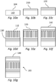
- Fig. 1 there is provided a cross sectional schematic for a semiconductor layer structure 100 comprising:
- the top surface 104 of the Si substrate 102 may have a Miller index of ⁇ 111 ⁇ .
- the Si substrate may be considered to have the face-centered diamond-cubic crystal structure.
- the Si substrate 102 and its top surface 104 may be substantially planar.
- the Si substrate 102 may have a vertical thickness in the range 100-1000 ⁇ m.
- the Si substrate 102 may more preferably have a vertical thickness in the range 275-525 ⁇ m. In general, and if not explicitly stated otherwise, thickness will herein refer to vertical thickness.
- the Si substrate 102 may be in the form of a substantially circular wafer preferably with a diameter larger than or equal to 1".
- the wafer may more preferably have a diameter in the range 2-12" and most preferably a diameter in the range 2-4".
- the first semiconductor layer 110 may preferably have a thickness in the range 100-500 nm and more preferably a thickness in the range 200-300 nm.
- the vertical nanowire structures 112 of the first semiconductor layer 110 may preferably have a vertical length in the range 50-500 nm and more preferably a vertical length in the range 150-250 nm.
- the vertical nanowire structures 112 may preferably have a substantially circular or hexagonal lateral cross section.
- the vertical nanowire structures 112 may preferably have a lateral diameter in the range 5-50 nm and more preferably a lateral diameter in the range 10-30 nm.
- the plurality of vertical nanowires 112 may be arranged in a repeating array pattern, as seen from the vertical direction.
- the repeating array pattern may be a hexagonal pattern, wherein each vertical nanowire structure 112 has six equidistant closest other vertical nanowire structures 112.
- the repeating array pattern may alternatively be a square pattern, wherein each vertical nanowire structure 112 has four equidistant closest other vertical nanowire structures 112.
- the distance to a closest other vertical nanowire structure 112 may preferably be in the range 10-500 nm.
- the closest distance may more preferably be in the range 50-200 nm. This closest distance may alternatively be understood as the spacing between vertical nanowire structures 112.
- the second semiconductor layer 120 may preferably have a thickness in the range 100-500 nm and more preferably a thickness in the range 200-300 nm.
- the second semiconductor layer 120 may be considered to laterally enclose, encapsulate, or encompass the vertical nanowire structures 112, i.e. filling in the space between the vertical nanowire structures 112.
- the second semiconductor layer 120 may further be considered to vertically enclose or encapsulate the vertical nanowire structures 112, i.e. extending vertically above and covering top portions of the vertical nanowire structures.
- the third and fourth semiconductor layers 130, 140 may be considered as relatively thin epilayers, i.e. epitaxially formed thin-film layers.
- the third semiconductor layer 130 may preferably have a thickness in the range 1-100 nm.
- the fourth semiconductor layer 140 may have a vertical thickness in the range 1-5 nm.
- the material may be considered to have the crystal structure wurtzite.
- the crystal structure may be aligned so that the C-plane, i.e. a plane with the Miller index ⁇ 0001 ⁇ , aligns with or is parallel with the top surface 104 of the Si substrate 102.
- the wurtzite crystal structure may additionally be considered for all further nitride-based layers and structures disclosed herein.
- the fourth semiconductor layer 140 may correspond to the wurtzite C-direction in such a way that a perpendicular C-plane may be obtained at an external surface of the thin-film.
- Such a C-plane surface may be considered an advantageous base for processing or fabricating many types of devices such as e.g. HEMTs and light-emitting diodes, LEDs,
- Fig. 2 shows the semiconductor layer structure 100 further comprising a bottom semiconductor layer 210, arranged intermediate to the top surface 104 of the substrate 102 and the first semiconductor layer 110, the bottom semiconductor 210 layer comprising AIN.
- the bottom semiconductor layer 210 may preferably have a thickness in the range 10-100 nm.
- Fig. 3 shows the semiconductor layer structure 100 further comprising an intermediate semiconductor layer 220, arranged intermediately to the bottom semiconductor layer 210 and the first semiconductor layer 110, the intermediate semiconductor layer 220 comprising AIN.
- the intermediate semiconductor layer 220 may preferably have a thickness in the range 10-100 nm.
- Fig. 4 shows the second semiconductor 120 layer comprising at least two vertically arranged sublayers 121,122, wherein x for a first sublayer 121 is greater than x for a second sublayer 122, wherein the second sublayer 122 is located further from the substrate than the first sublayer 121.
- One exemplary second semiconductor layer 120 may comprise three vertically arranged sublayers.
- the sublayers 121, 122 may each have a thickness in the range 20-250 nm.
- a high-electron-mobility transistor device 300 comprising:
- the source and drain contacts 301, 303 may comprise metal materials such as Ti, Al, Cu, Ni, and/or Au.
- the source and drain contacts 301, 303 may comprise compounds or alloys such as e.g. AlCu.
- the gate contact 305 may, in addition to the materials mentioned for the source and drain contacts 301, 303, comprise Pd and/or Au. As for the source and drain contacts 301, 303, compounds and alloys are also options for the gate contact 305.
- the HEMT 300 may further comprise an oxide layer 310 arranged on the semiconductor layers 130, 140.
- the oxide layer 310 may be configured to feature a low relative permittivity material to reduce parasitic capacitances between the source, drain, and gate contacts 301, 303, 305.
- the oxide layer may comprise SiO 2 , or other types of Si-based oxides.
- the third semiconductor layer comprising Al y Ga 1-y N, may be considered a barrier layer of the HEMT 300.
- Fig. 6 shows the fourth semiconductor layer 140 being arranged as a vertical fin 307, wherein the vertical fin 307 is arranged directly adjacent on the third semiconductor layer 130, wherein the gate contact 305 is arranged to laterally and vertically enclose the vertical fin 307, and wherein the vertical fin 307 comprises p-doped GaN.
- the vertical fin 307 may be etched out of the fourth semiconductor layer 140.
- the vertical fin 307 may be understood as a laterally elongated fin or alternatively as a laterally shorter mesa structure.
- Impurity atoms, for p-doping of GaN may comprise elements from the second group of the periodic table of elements e.g. Mg. Impurities may be activated through e.g. thermal processing/annealing or electron bombardment/irradiation.
- the fourth semiconductor layer 140 may further not form a continuous layer between the source, drain and gate contacts 301, 303, 305, as in the case of Fig. 5 .
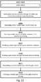
- Fig. 7 there is provided a flowchart for a method for producing a semiconductor layer structure 100, the method comprising:
- the Si substrate 102 may be formed using conventional Si wafer production methods including e.g. the aforementioned Czochralski process.
- the first semiconductor layer 110 may be formed S4003 using physical vapor deposition, PVD, chemical vapor deposition, CVD, plasma-enhanced chemical vapor deposition, PECVD, metalorganic chemical vapor deposition, MOCVD, metalorganic vapor-phase epitaxy, MOVPE, sputtering, or similar methods.
- the vertical nanowire structures 112 of the first semiconductor layer 110 may be formed using etching methods such as dry etching, wet etching, chemical etching, plasma etching, reactive ion etching, etc. The etching may be performed subsequent to a patterning step aiming to define the nanowire structures 112.
- the vertical nanowire structures 112 may additionally be formed using epitaxy methods such as MOCVD or MOVPE, both essentially referring to the same technique. Selective area growth, based on the preceding patterning, may be employed for the nanowire structures 112.
- Patterning, pattern transferring, or defining of the nanowire structures 112 may be lithography based.
- Optical lithography such as ultraviolet, UV, lithography may be employed.
- Electron beam lithography, EBL, or nanoimprint lithography, NIL, as well as various other similar lithography methods may be employed.
- patterning may comprise just etching, or depositing, through a solid mask aligned onto, or close to, the surface of the layer or structure to be etched or deposited onto.
- Fig. 7 also shows how the method may further comprise depositing S5007 a bottom semiconductor layer 210 intermediate to providing S4001 the substrate 102 and forming S4003 the first semiconductor layer 110, the bottom semiconductor layer 210 comprising AIN.
- the bottom layer 210 may be deposited S5007 using similar methods as the first semiconductor layer 110.
- the bottom layer 120 may preferably be deposited using PVD.
- Fig. 7 also shows how the method may further comprise depositing S5009 an intermediate semiconductor layer 220 intermediate to depositing S5007 the bottom semiconductor layer 210 and forming S4003 the first semiconductor layer 110, the intermediate semiconductor layer 220 comprising AIN.
- the intermediate layer 220 may be deposited S5009 using similar methods as the first semiconductor layer 110.
- the intermediate layer 220 may preferably be deposited using high temperature MOCVD/MOVPE.
- the second, third, and fourth semiconductor layers 120, 130, 140 may be deposited S4005, S4007, S4009 using MOCVD/MOVPE.
- Different precursor gas pressure and temperatures may be used to create solid crystal material of different compositions ranging from AIN, through various compositions of AIGaN, to GaN. It is preferred to use a temperature equal or higher than 1000°C for the GaN MOCVD/MOVPE.
- Precursor gases may comprise trimethylaluminium, TMAI, triethylaluminium, TEAI, trimethylgallium, TMGa, triethylgallium, TEGa, phenyl hydrazine, dimethylhydrazine, DMHy, tertiarybutylamine, TBAm, ammonia, NH3.
- the step of depositing S4005 a second semiconductor layer 120 may be understood as epitaxially growing a shell, or shells, laterally or radially out, from the vertical nanowire structures 112, in the M-direction of the wurtzite crystal of the vertical nanowire structures 112.
- the shell, or shells, from different vertical nanowire structures 112 may coalesce to form a common thin-film being the second semiconductor layer 120.
- Fig. 8 shows how forming said plurality of vertical nanowire structures 112 of said first semiconductor layer 110 may comprise:
- the etching S5003 may be a selective etching procedure, e.g. based on a preceding patterning step.
- the etching S5003 may produce the vertical nanowire structures 112.
- the etching S5003 may be e.g. a chlorine-based plasma etching procedure.
- Fig. 8 further shows how forming said plurality of vertical nanowire structures 112 may comprise epitaxially, e.g. through selective area growth MOCVD/MOVPE, forming S5005 the plurality of vertical nanowire structures 112 on the substrate 102.
- Fig. 9 shows how forming said second semiconductor layer 120 may comprise:
- Differences in composition of the sublayers 121, 122 may be achieved by gradually changing parameters such as temperature and precursor gas pressure.
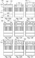
- Figs. 10a-g show cross sectional views at different chronological stages of the method for producing the semiconductor layer structure.
- Fig. 10a shows just the provided S4001 substrate 102, with its top surface 104.
- Fig. 10b shows a bottom semiconductor layer 210 deposited S5007 onto the top surface 104 of the substrate 102.
- Fig. 10c shows an intermediate semiconductor layer 220 deposited S5009 onto the bottom semiconductor layer 210.
- Fig. 10d shows the first semiconductor layer 110, including the vertical nanowires structures 112, formed S4003 onto the intermediate semiconductor layer 220. Note that the first semiconductor layer 110 may be formed S4003 directly onto the top surface 104 of the substrate 102.
- Fig. 10e shows the second semiconductor layer 120 deposited S4005 onto the first semiconductor layer 110, laterally and vertically enclosing the nanowire structures 112.
- Fig. 10f shows the third semiconductor layer 130 deposited S4007 onto the second semiconductor layer 120.
- Fig. 10g shows a completed semiconductor layer structure 100 with the fourth semiconductor layer 140 deposited S4009 onto the third semiconductor layer 130.
- Fig. 11 there is provided a flowchart for a method for producing a high-electron-mobility transistor device 300, the method comprising:
- the forming S6001 of the at least two trenches 702, as well as the forming S6009 of the gate trench 708 may comprise selective etching based on patterning, as described in the above. Patterning may be performed similar for all trenches 702, 708 but etching may need to be customized according to the material to be etched. E.g. a plasma-based etching may be used for forming S6001 the at least two trenches 702 through the third and fourth semiconductor layers 130, 140.
- An oxide etch method e.g. hydrofluoric acid, HF, wet etch, may be used for forming S6009 the gate trench 708 through the oxide layer 310.
- the trenches 702, 708 may be understood as laterally elongated trenches or alternatively as laterally shorter pits.
- first and second metallic layers 704, 708 may be performed by e.g. sputtering or metal evaporation.
- first metallic layer 704 may comprise the same materials as described in the above in relation to the metallic source and drain contacts 301, 303.
- second metallic layer 708 may comprise the same materials as described in the above in relation to the metallic gate contact 305.
- the forming S6005, S6013 of the source, drain, and gate contacts 301, 303, 305 may be performed by etching the first and second metallic layers 704, 708 using a metal etch method suitable for the metallic material to be etched. Once again, etching may be mediated through a patterning step to define areas of the layer to remove. Such a patterning step may be performed in accordance with above mentioned methods of patterning.
- the forming S6007 of the oxide layer 310 may comprise deposition such an oxide layer 310 through deposition methods described in the above. E.g. CVD, PECVD and sputtering may be utilized for forming the oxide layer 310.
- Figs. 12a-g show cross sectional views at different chronological stages of the method for producing the HEMT 300.
- Fig. 12a shows a semiconductor layer structure 100, being the base for a following steps of producing the HEMT 300.
- Fig. 12b shows the at least two trenches 702 formed S6001 through the third and fourth semiconductor layers 130, 140.
- Fig. 12c shows the first metallic layer 704 deposited S6003 into the trenches 702, onto the second semiconductor layer 120.
- Fig. 12d shows the metallic source and drain contacts 301, 303 formed S6005 in the trenches 702 by selective removal of portions of the first metallic layer 704 that initially physically connected the source and drain contacts 301, 303.
- Fig. 12e shows the oxide layer 301 formed S6007 onto source and drain contacts 301, 303 and the semiconductor layers.
- Fig. 12f shows the gate trench 708 formed S6009 through the oxide layer 310, laterally between the source and drain contacts 301, 303.
- Fig. 12g shows the second metallic layer 710 deposited S6011 into the gate trench 708, onto the fourth semiconductor layer 140.
- the HEMT 300 may now be considered complete.
- Fig. 12i shows an additional step of planarizing the top portions of the HEMT 300. This may be done in order to simplify access to the source and drain contacts 301, 303 and reduce interconnect complexity. Chemical mechanical polishing, CMP, may be utilized for such a planarizing step.
- Fig. 13 shows a top view of a HEMT 300 contact layout.
- the source contact 301, the drain contact 303, and the gate contact 305 are herein arranged in a multi-finger layout.
- the source contact 301 has three fingers and the drain contact has two fingers.
- the gate contact 305 is shown to meander between the source and drain contacts 301, 303.
- a HEMT device cross section as e.g. the one shown in Fig. 5 , may be understood to correspond with the cross section 802 indicated in Fig. 13 .
- the layout furthers efficient area spacing of devices and evenly distributed electric currents.
- the layout allows for higher currents due to a longer effective channel width.
- the effective channel width may be understood as the total number of fingers (both source and drain) minus one, all multiplied with the length of one finger.
- the layout may also reduce the gate resistance and prevent a low-pass filter to form with the gate channel capacitance. Hence HEMT switching speed is improved by such a layout.
Priority Applications (12)
| Application Number | Priority Date | Filing Date | Title |
|---|---|---|---|
| EP19215267.6A EP3836227A1 (de) | 2019-12-11 | 2019-12-11 | Halbleiterschichtstruktur |
| TW109140371A TW202122649A (zh) | 2019-12-11 | 2020-11-18 | 半導體層結構,基於半導體層結構的高電子遷移率電晶體元件,以及其製造方法 |
| EP24164181.0A EP4362104A2 (de) | 2019-12-11 | 2020-12-08 | Halbleiterschichtstruktur |
| JP2022533545A JP2023505767A (ja) | 2019-12-11 | 2020-12-08 | 半導体層構造 |
| EP20817032.4A EP4073847B1 (de) | 2019-12-11 | 2020-12-08 | Halbleiterschichtstruktur |
| PCT/EP2020/085010 WO2021116073A1 (en) | 2019-12-11 | 2020-12-08 | Semiconductor layer structure |
| AU2020400286A AU2020400286B2 (en) | 2019-12-11 | 2020-12-08 | Semiconductor layer structure |
| KR1020227023222A KR20220110824A (ko) | 2019-12-11 | 2020-12-08 | 반도체 층 구조물 |
| CN202080083021.8A CN114788013A (zh) | 2019-12-11 | 2020-12-08 | 半导体层结构 |
| US17/806,400 US11695066B2 (en) | 2019-12-11 | 2022-06-10 | Semiconductor layer structure |
| US18/321,643 US20230327009A1 (en) | 2019-12-11 | 2023-05-22 | Semiconductor layer structure |
| AU2023210648A AU2023210648A1 (en) | 2019-12-11 | 2023-08-04 | Semiconductor layer structure |
Applications Claiming Priority (1)
| Application Number | Priority Date | Filing Date | Title |
|---|---|---|---|
| EP19215267.6A EP3836227A1 (de) | 2019-12-11 | 2019-12-11 | Halbleiterschichtstruktur |
Publications (1)
| Publication Number | Publication Date |
|---|---|
| EP3836227A1 true EP3836227A1 (de) | 2021-06-16 |
Family
ID=68887205
Family Applications (3)
| Application Number | Title | Priority Date | Filing Date |
|---|---|---|---|
| EP19215267.6A Withdrawn EP3836227A1 (de) | 2019-12-11 | 2019-12-11 | Halbleiterschichtstruktur |
| EP24164181.0A Pending EP4362104A2 (de) | 2019-12-11 | 2020-12-08 | Halbleiterschichtstruktur |
| EP20817032.4A Active EP4073847B1 (de) | 2019-12-11 | 2020-12-08 | Halbleiterschichtstruktur |
Family Applications After (2)
| Application Number | Title | Priority Date | Filing Date |
|---|---|---|---|
| EP24164181.0A Pending EP4362104A2 (de) | 2019-12-11 | 2020-12-08 | Halbleiterschichtstruktur |
| EP20817032.4A Active EP4073847B1 (de) | 2019-12-11 | 2020-12-08 | Halbleiterschichtstruktur |
Country Status (8)
| Country | Link |
|---|---|
| US (2) | US11695066B2 (de) |
| EP (3) | EP3836227A1 (de) |
| JP (1) | JP2023505767A (de) |
| KR (1) | KR20220110824A (de) |
| CN (1) | CN114788013A (de) |
| AU (2) | AU2020400286B2 (de) |
| TW (1) | TW202122649A (de) |
| WO (1) | WO2021116073A1 (de) |
Families Citing this family (2)
| Publication number | Priority date | Publication date | Assignee | Title |
|---|---|---|---|---|
| EP4101945B1 (de) | 2021-06-09 | 2024-05-15 | Epinovatech AB | Vorrichtung zur durchführung von wasserelektrolyse und system dafür |
| CN113394284B (zh) * | 2021-06-25 | 2023-04-14 | 电子科技大学 | 具有复合层结构的高压mis-hemt器件 |
Citations (2)
| Publication number | Priority date | Publication date | Assignee | Title |
|---|---|---|---|---|
| US20140134773A1 (en) * | 2011-10-10 | 2014-05-15 | Sensor Electronic Technology, Inc. | Patterned Layer Design for Group III Nitride Layer Growth |
| US20190081164A1 (en) * | 2017-07-12 | 2019-03-14 | Indian Institute Of Science | A High-electron-mobility transistor (HEMT) |
Family Cites Families (69)
| Publication number | Priority date | Publication date | Assignee | Title |
|---|---|---|---|---|
| US2463073A (en) | 1945-01-26 | 1949-03-01 | Rca Corp | Oscillator |
| US4103325A (en) | 1977-03-18 | 1978-07-25 | Sperry Rand Corporation | Aircraft power and phase converter |
| EP0284700A1 (de) | 1987-03-31 | 1988-10-05 | Marthaler, Willy | Zum Tragen durch Personen bestimmter Halter für eine Uhr oder ein Schmuckstück |
| US4873497A (en) | 1988-10-03 | 1989-10-10 | Motorola, Inc. | Wide band voltage controlled R-C oscillator for use with MMIC technology |
| WO1995008452A1 (en) | 1993-09-23 | 1995-03-30 | Stichting Voor De Technische Wetenschappen | Control method and circuit for an induction motor |
| US6107653A (en) | 1997-06-24 | 2000-08-22 | Massachusetts Institute Of Technology | Controlling threading dislocation densities in Ge on Si using graded GeSi layers and planarization |
| AU2003210961A1 (en) | 2002-02-11 | 2003-09-04 | Rensselaer Polytechnic Institute | Directed assembly of highly-organized carbon nanotube architectures |
| KR100593264B1 (ko) | 2003-06-26 | 2006-06-26 | 학교법인 포항공과대학교 | p-타입 반도체 박막과 n-타입 산화아연(ZnO)계나노막대의 이종접합 구조체, 이의 제법 및 이를 이용한소자 |
| KR100664986B1 (ko) | 2004-10-29 | 2007-01-09 | 삼성전기주식회사 | 나노로드를 이용한 질화물계 반도체 소자 및 그 제조 방법 |
| US7202173B2 (en) | 2004-12-20 | 2007-04-10 | Palo Alto Research Corporation Incorporated | Systems and methods for electrical contacts to arrays of vertically aligned nanorods |
| US20070108435A1 (en) | 2005-02-07 | 2007-05-17 | Harmon Eric S | Method of making nanowires |
| US8044432B2 (en) | 2005-11-29 | 2011-10-25 | The Hong Kong University Of Science And Technology | Low density drain HEMTs |
| US7968359B2 (en) | 2006-03-10 | 2011-06-28 | Stc.Unm | Thin-walled structures |
| AU2007313096B2 (en) | 2006-03-10 | 2011-11-10 | Unm Rainforest Innovations | Pulsed growth of GaN nanowires and applications in group III nitride semiconductor substrate materials and devices |
| JP2009530862A (ja) | 2006-03-20 | 2009-08-27 | インターナショナル レクティファイアー コーポレイション | 併合ゲートカスコードトランジスタ |
| JP4807186B2 (ja) | 2006-08-30 | 2011-11-02 | マツダ株式会社 | フリーピストンエンジンの制御装置 |
| JP2010503981A (ja) | 2006-09-19 | 2010-02-04 | クナノ アーベー | ナノスケール電界効果トランジスタの構体 |
| TW200835126A (en) | 2006-11-28 | 2008-08-16 | Int Rectifier Corp | Synchronous DC/DC converter |
| FR2910721B1 (fr) | 2006-12-21 | 2009-03-27 | Commissariat Energie Atomique | Ensemble collecteur de courant-electrode avec des cavites d'expansion pour accumulateur au lithium sous forme de films minces. |
| US7829443B2 (en) | 2007-01-12 | 2010-11-09 | Qunano Ab | Nitride nanowires and method of producing such |
| US20080171424A1 (en) | 2007-01-16 | 2008-07-17 | Sharp Laboratories Of America, Inc. | Epitaxial growth of GaN and SiC on silicon using nanowires and nanosize nucleus methodologies |
| JP5341325B2 (ja) | 2007-07-25 | 2013-11-13 | 日本化学工業株式会社 | リチウム二次電池用正極活物質、その製造方法及びリチウム二次電池 |
| US20110036396A1 (en) | 2008-04-30 | 2011-02-17 | The Regents Of The University Of California | Method and apparatus for fabricating optoelectromechanical devices by structural transfer using re-usable substrate |
| WO2010022064A1 (en) | 2008-08-21 | 2010-02-25 | Nanocrystal Corporation | Defect-free group iii - nitride nanostructures and devices using pulsed and non-pulsed growth techniques |
| US9275857B1 (en) | 2008-12-19 | 2016-03-01 | Stc.Unm | Nanowires, nanowire networks and methods for their formation and use |
| WO2010100599A1 (en) | 2009-03-04 | 2010-09-10 | Koninklijke Philips Electronics, N.V. | Large capacity thin film battery and method for making same |
| JP5182189B2 (ja) | 2009-03-27 | 2013-04-10 | 富士通株式会社 | 半導体装置の製造方法 |
| US9502973B2 (en) | 2009-04-08 | 2016-11-22 | Infineon Technologies Americas Corp. | Buck converter with III-nitride switch for substantially increased input-to-output voltage ratio |
| CN101621292B (zh) | 2009-04-10 | 2012-05-09 | 浙江大学 | 开关电容积分器 |
| JP5299105B2 (ja) | 2009-06-16 | 2013-09-25 | ソニー株式会社 | 二酸化バナジウムナノワイヤとその製造方法、及び二酸化バナジウムナノワイヤを用いたナノワイヤデバイス |
| US8895958B2 (en) | 2009-12-01 | 2014-11-25 | National University Corporation Hokkaido University | Light emitting element and method for manufacturing same |
| EP2571065A4 (de) | 2010-12-08 | 2016-03-23 | El Seed Corp | Gruppe-iii-nitrid-halbleitervorrichtung und herstellungsverfahren dafür |
| GB201021112D0 (en) | 2010-12-13 | 2011-01-26 | Ntnu Technology Transfer As | Nanowires |
| WO2012105901A1 (en) | 2011-02-01 | 2012-08-09 | Qunano Ab | Lithium-ion battery comprising nanowires |
| US8758480B2 (en) | 2011-09-09 | 2014-06-24 | Torosoleil, Llc | Dynamic and continuous control for pressure swing adsorption |
| GB201200355D0 (en) | 2012-01-10 | 2012-02-22 | Norwegian Univ Sci & Tech Ntnu | Nanowires |
| JP2013153027A (ja) | 2012-01-24 | 2013-08-08 | Fujitsu Ltd | 半導体装置及び電源装置 |
| EP2815423B1 (de) * | 2012-02-14 | 2017-05-24 | Hexagem AB | Galliumnitrid-nanodraht basierte elektronik |
| TWI617045B (zh) | 2012-07-06 | 2018-03-01 | 晶元光電股份有限公司 | 具有奈米柱之發光元件及其製造方法 |
| FR3000294B1 (fr) | 2012-12-21 | 2016-03-04 | Aledia | Support fonctionnel comprenant des nanofils et des nano-empreintes et procede de fabrication dudit support |
| US9251934B2 (en) | 2013-01-11 | 2016-02-02 | Infineon Technologies Ag | Method for manufacturing a plurality of nanowires |
| US8823146B1 (en) | 2013-02-19 | 2014-09-02 | Raytheon Company | Semiconductor structure having silicon devices, column III-nitride devices, and column III-non-nitride or column II-VI devices |
| JP2014217252A (ja) | 2013-04-30 | 2014-11-17 | 三菱電機株式会社 | カスコード接続パワーデバイス |
| US9349715B2 (en) | 2013-06-21 | 2016-05-24 | Infineon Technologies Americas Corp. | Depletion mode group III-V transistor with high voltage group IV enable switch |
| JP6175931B2 (ja) | 2013-06-21 | 2017-08-09 | 富士通株式会社 | 導電構造及びその製造方法、電子装置及びその製造方法 |
| US9640645B2 (en) | 2013-09-05 | 2017-05-02 | Taiwan Semiconductor Manufacturing Company Limited | Semiconductor device with silicide |
| JP6237038B2 (ja) | 2013-09-20 | 2017-11-29 | 富士通株式会社 | カスコードトランジスタ及びカスコードトランジスタの制御方法 |
| US20150118572A1 (en) | 2013-10-29 | 2015-04-30 | Battery Energy Storage Systems-Technologies | Solid-state battery and methods of fabrication |
| GB2520687A (en) | 2013-11-27 | 2015-06-03 | Seren Photonics Ltd | Semiconductor devices and fabrication methods |
| KR102205699B1 (ko) * | 2014-04-11 | 2021-01-21 | 삼성전자주식회사 | 양자점을 갖는 전자소자 및 그 제조방법 |
| JP6256598B2 (ja) | 2014-04-14 | 2018-01-10 | 富士通株式会社 | 光合成装置 |
| GB201407297D0 (en) | 2014-04-25 | 2014-06-11 | Gasp Solar Aps | A method of preparing a substrate for nanowire growth, And a method of fabricating an array of semiconductor nanostructures |
| US9893174B2 (en) | 2014-05-21 | 2018-02-13 | Arizona Board Of Regents On Behalf Of Arizona State University | III-nitride based N polar vertical tunnel transistor |
| US9773669B2 (en) | 2014-09-11 | 2017-09-26 | Ramot At Tel-Aviv University Ltd. | Method of fabricating a nanoribbon and applications thereof |
| US9406506B2 (en) | 2014-11-05 | 2016-08-02 | International Business Machines Corporation | Lattice matched aspect ratio trapping to reduce defects in III-V layer directly grown on silicon |
| US9520466B2 (en) | 2015-03-16 | 2016-12-13 | Taiwan Semiconductor Manufacturing Company, Ltd. | Vertical gate-all-around field effect transistors and methods of forming same |
| CN106549050A (zh) | 2015-09-17 | 2017-03-29 | 中国科学院苏州纳米技术与纳米仿生研究所 | 级联增强型hemt器件 |
| US9916985B2 (en) | 2015-10-14 | 2018-03-13 | International Business Machines Corporation | Indium phosphide smoothing and chemical mechanical planarization processes |
| WO2017111844A1 (en) | 2015-12-24 | 2017-06-29 | Intel Corporation | Memory devices including integrated tunnel diode in contact and techniques for forming same |
| US11018253B2 (en) | 2016-01-07 | 2021-05-25 | Lawrence Livermore National Security, Llc | Three dimensional vertically structured electronic devices |
| US10128750B2 (en) | 2016-03-04 | 2018-11-13 | Infineon Technologies Ag | Switched-mode power converter with an inductive storage element and a cascode circuit |
| US10312082B2 (en) | 2016-05-09 | 2019-06-04 | The Regents Of The University Of Michigan | Metal based nanowire tunnel junctions |
| WO2017213644A1 (en) | 2016-06-08 | 2017-12-14 | Intel Corporation | Monolithic integration of back-end p-channel transistor with iii-n n-channel transistor |
| JP6816735B2 (ja) | 2018-03-13 | 2021-01-20 | 株式会社豊田中央研究所 | 化学反応用電極、それを用いた化学反応用セル及び化学反応装置 |
| KR102508471B1 (ko) | 2018-04-22 | 2023-03-10 | 에피노바테크 에이비 | 강화 박막 필름 장치 |
| US10594268B2 (en) | 2018-05-18 | 2020-03-17 | Cree, Inc. | Switch circuits having integrated overdrive protection and related transmit/receive circuits and MMIC amplifiers |
| US10535570B1 (en) | 2018-06-22 | 2020-01-14 | International Business Machines Corporation | Cointegration of III-V channels and germanium channels for vertical field effect transistors |
| CN110336028B (zh) | 2019-04-30 | 2021-03-30 | 中国科学院半导体研究所 | 电池负极材料及其制备方法、锂电池 |
| EP3855530A1 (de) | 2020-01-24 | 2021-07-28 | Epinovatech AB | Feststoffbatterie |
-
2019
- 2019-12-11 EP EP19215267.6A patent/EP3836227A1/de not_active Withdrawn
-
2020
- 2020-11-18 TW TW109140371A patent/TW202122649A/zh unknown
- 2020-12-08 JP JP2022533545A patent/JP2023505767A/ja active Pending
- 2020-12-08 EP EP24164181.0A patent/EP4362104A2/de active Pending
- 2020-12-08 WO PCT/EP2020/085010 patent/WO2021116073A1/en active Search and Examination
- 2020-12-08 AU AU2020400286A patent/AU2020400286B2/en active Active
- 2020-12-08 CN CN202080083021.8A patent/CN114788013A/zh active Pending
- 2020-12-08 EP EP20817032.4A patent/EP4073847B1/de active Active
- 2020-12-08 KR KR1020227023222A patent/KR20220110824A/ko unknown
-
2022
- 2022-06-10 US US17/806,400 patent/US11695066B2/en active Active
-
2023
- 2023-05-22 US US18/321,643 patent/US20230327009A1/en active Pending
- 2023-08-04 AU AU2023210648A patent/AU2023210648A1/en active Pending
Patent Citations (2)
| Publication number | Priority date | Publication date | Assignee | Title |
|---|---|---|---|---|
| US20140134773A1 (en) * | 2011-10-10 | 2014-05-15 | Sensor Electronic Technology, Inc. | Patterned Layer Design for Group III Nitride Layer Growth |
| US20190081164A1 (en) * | 2017-07-12 | 2019-03-14 | Indian Institute Of Science | A High-electron-mobility transistor (HEMT) |
Non-Patent Citations (2)
| Title |
|---|
| SUNDARAM S ET AL: "Single-crystal nanopyramidal BGaN by nanoselective area growth on AlN/Si(111) and GaN templates", NANOTECHNOLOGY, INSTITUTE OF PHYSICS PUBLISHING, GB, vol. 27, no. 11, 15 February 2016 (2016-02-15), pages 115602, XP020301373, ISSN: 0957-4484, [retrieved on 20160215], DOI: 10.1088/0957-4484/27/11/115602 * |
| TRIPATHY S ET AL: "AlGaN/GaN two-dimensional-electron gas heterostructures on 200 mm diameter Si(111)", APPLIED PHYSICS LETTERS, A I P PUBLISHING LLC, US, vol. 101, no. 8, 20 August 2012 (2012-08-20), pages 82110 - 82110, XP012164818, ISSN: 0003-6951, [retrieved on 20120823], DOI: 10.1063/1.4746751 * |
Also Published As
| Publication number | Publication date |
|---|---|
| US20220302293A1 (en) | 2022-09-22 |
| AU2023210648A1 (en) | 2023-08-24 |
| JP2023505767A (ja) | 2023-02-13 |
| TW202122649A (zh) | 2021-06-16 |
| EP4073847B1 (de) | 2024-04-24 |
| EP4362104A2 (de) | 2024-05-01 |
| AU2020400286B2 (en) | 2023-06-15 |
| US11695066B2 (en) | 2023-07-04 |
| CN114788013A (zh) | 2022-07-22 |
| AU2020400286A1 (en) | 2022-06-09 |
| KR20220110824A (ko) | 2022-08-09 |
| EP4073847A1 (de) | 2022-10-19 |
| US20230327009A1 (en) | 2023-10-12 |
| WO2021116073A1 (en) | 2021-06-17 |
Similar Documents
| Publication | Publication Date | Title |
|---|---|---|
| EP2602827B1 (de) | Anreicherungsmodus III-Nitridvorrichtung, und Verfahren zur Herstellung davon | |
| US20230327009A1 (en) | Semiconductor layer structure | |
| US8772831B2 (en) | III-nitride growth method on silicon substrate | |
| US9224847B2 (en) | High electron mobility transistor and method of forming the same | |
| EP2973658A1 (de) | Reo-gate-dielektrikum für eine iii-n-vorrichtung auf einem si-substrat | |
| US8723296B2 (en) | Stress compensation for large area gallium nitride or other nitride-based structures on semiconductor substrates | |
| US20150349064A1 (en) | Nucleation and buffer layers for group iii-nitride based semiconductor devices | |
| JP2007165431A (ja) | 電界効果型トランジスタおよびその製造方法 | |
| JP2011238931A (ja) | エンハンスメントモード電界効果デバイスおよびそれを製造する方法 | |
| JP7013710B2 (ja) | 窒化物半導体トランジスタの製造方法 | |
| US11876129B2 (en) | Semiconductor structure and manufacturing method for the semiconductor structure | |
| KR20150000753A (ko) | 질화물 반도체 소자 및 그 제조 방법 | |
| CN106910770B (zh) | 氮化镓基反相器芯片及其形成方法 | |
| KR102077674B1 (ko) | 질화물 반도체 소자 및 그 제조 방법 | |
| US10756235B2 (en) | Stripped method for preparing semiconductor structure | |
| CN107046053B (zh) | 半导体结构及其制造方法 | |
| KR20140139890A (ko) | 질화물 반도체 소자 및 그 제조 방법 | |
| US11450764B2 (en) | Semiconductor device and method of forming the same | |
| WO2024040019A1 (en) | Semiconductor structures and fabrication using sublimation | |
| KR102080744B1 (ko) | 질화물 반도체 소자 및 그 제조 방법 | |
| KR20150000752A (ko) | 질화물 반도체 소자 및 그 제조 방법 | |
| CN114695115A (zh) | 一种具有鳍式结构的半导体器件及其制备方法 |
Legal Events
| Date | Code | Title | Description |
|---|---|---|---|
| PUAI | Public reference made under article 153(3) epc to a published international application that has entered the european phase |
Free format text: ORIGINAL CODE: 0009012 |
|
| STAA | Information on the status of an ep patent application or granted ep patent |
Free format text: STATUS: THE APPLICATION HAS BEEN PUBLISHED |
|
| AK | Designated contracting states |
Kind code of ref document: A1 Designated state(s): AL AT BE BG CH CY CZ DE DK EE ES FI FR GB GR HR HU IE IS IT LI LT LU LV MC MK MT NL NO PL PT RO RS SE SI SK SM TR |
|
| STAA | Information on the status of an ep patent application or granted ep patent |
Free format text: STATUS: THE APPLICATION IS DEEMED TO BE WITHDRAWN |
|
| 18D | Application deemed to be withdrawn |
Effective date: 20211217 |