EP3836201B1 - Halbleiterschaltelement und verfahren zur herstellung davon - Google Patents
Halbleiterschaltelement und verfahren zur herstellung davon Download PDFInfo
- Publication number
- EP3836201B1 EP3836201B1 EP19215271.8A EP19215271A EP3836201B1 EP 3836201 B1 EP3836201 B1 EP 3836201B1 EP 19215271 A EP19215271 A EP 19215271A EP 3836201 B1 EP3836201 B1 EP 3836201B1
- Authority
- EP
- European Patent Office
- Prior art keywords
- substrate
- trenches
- trench
- switch element
- semiconductor switch
- Prior art date
- Legal status (The legal status is an assumption and is not a legal conclusion. Google has not performed a legal analysis and makes no representation as to the accuracy of the status listed.)
- Active
Links
Images





Classifications
-
- H—ELECTRICITY
- H10—SEMICONDUCTOR DEVICES; ELECTRIC SOLID-STATE DEVICES NOT OTHERWISE PROVIDED FOR
- H10B—ELECTRONIC MEMORY DEVICES
- H10B63/00—Resistance change memory devices, e.g. resistive RAM [ReRAM] devices
- H10B63/30—Resistance change memory devices, e.g. resistive RAM [ReRAM] devices comprising selection components having three or more electrodes, e.g. transistors
- H10B63/34—Resistance change memory devices, e.g. resistive RAM [ReRAM] devices comprising selection components having three or more electrodes, e.g. transistors of the vertical channel field-effect transistor type
-
- H—ELECTRICITY
- H10—SEMICONDUCTOR DEVICES; ELECTRIC SOLID-STATE DEVICES NOT OTHERWISE PROVIDED FOR
- H10D—INORGANIC ELECTRIC SEMICONDUCTOR DEVICES
- H10D30/00—Field-effect transistors [FET]
- H10D30/01—Manufacture or treatment
- H10D30/021—Manufacture or treatment of FETs having insulated gates [IGFET]
- H10D30/025—Manufacture or treatment of FETs having insulated gates [IGFET] of vertical IGFETs
-
- H—ELECTRICITY
- H10—SEMICONDUCTOR DEVICES; ELECTRIC SOLID-STATE DEVICES NOT OTHERWISE PROVIDED FOR
- H10D—INORGANIC ELECTRIC SEMICONDUCTOR DEVICES
- H10D30/00—Field-effect transistors [FET]
- H10D30/60—Insulated-gate field-effect transistors [IGFET]
- H10D30/63—Vertical IGFETs
-
- H—ELECTRICITY
- H10—SEMICONDUCTOR DEVICES; ELECTRIC SOLID-STATE DEVICES NOT OTHERWISE PROVIDED FOR
- H10D—INORGANIC ELECTRIC SEMICONDUCTOR DEVICES
- H10D30/00—Field-effect transistors [FET]
- H10D30/60—Insulated-gate field-effect transistors [IGFET]
- H10D30/64—Double-diffused metal-oxide semiconductor [DMOS] FETs
- H10D30/66—Vertical DMOS [VDMOS] FETs
- H10D30/668—Vertical DMOS [VDMOS] FETs having trench gate electrodes, e.g. UMOS transistors
-
- H—ELECTRICITY
- H10—SEMICONDUCTOR DEVICES; ELECTRIC SOLID-STATE DEVICES NOT OTHERWISE PROVIDED FOR
- H10D—INORGANIC ELECTRIC SEMICONDUCTOR DEVICES
- H10D64/00—Electrodes of devices having potential barriers
- H10D64/01—Manufacture or treatment
-
- H—ELECTRICITY
- H10—SEMICONDUCTOR DEVICES; ELECTRIC SOLID-STATE DEVICES NOT OTHERWISE PROVIDED FOR
- H10D—INORGANIC ELECTRIC SEMICONDUCTOR DEVICES
- H10D64/00—Electrodes of devices having potential barriers
- H10D64/111—Field plates
- H10D64/117—Recessed field plates, e.g. trench field plates or buried field plates
-
- H—ELECTRICITY
- H10—SEMICONDUCTOR DEVICES; ELECTRIC SOLID-STATE DEVICES NOT OTHERWISE PROVIDED FOR
- H10D—INORGANIC ELECTRIC SEMICONDUCTOR DEVICES
- H10D64/00—Electrodes of devices having potential barriers
- H10D64/20—Electrodes characterised by their shapes, relative sizes or dispositions
- H10D64/23—Electrodes carrying the current to be rectified, amplified, oscillated or switched, e.g. sources, drains, anodes or cathodes
- H10D64/251—Source or drain electrodes for field-effect devices
- H10D64/252—Source or drain electrodes for field-effect devices for vertical or pseudo-vertical devices
-
- H—ELECTRICITY
- H10—SEMICONDUCTOR DEVICES; ELECTRIC SOLID-STATE DEVICES NOT OTHERWISE PROVIDED FOR
- H10D—INORGANIC ELECTRIC SEMICONDUCTOR DEVICES
- H10D84/00—Integrated devices formed in or on semiconductor substrates that comprise only semiconducting layers, e.g. on Si wafers or on GaAs-on-Si wafers
- H10D84/01—Manufacture or treatment
- H10D84/0123—Integrating together multiple components covered by H10D12/00 or H10D30/00, e.g. integrating multiple IGBTs
- H10D84/0126—Integrating together multiple components covered by H10D12/00 or H10D30/00, e.g. integrating multiple IGBTs the components including insulated gates, e.g. IGFETs
- H10D84/0149—Manufacturing their interconnections or electrodes, e.g. source or drain electrodes
-
- H—ELECTRICITY
- H10—SEMICONDUCTOR DEVICES; ELECTRIC SOLID-STATE DEVICES NOT OTHERWISE PROVIDED FOR
- H10D—INORGANIC ELECTRIC SEMICONDUCTOR DEVICES
- H10D84/00—Integrated devices formed in or on semiconductor substrates that comprise only semiconducting layers, e.g. on Si wafers or on GaAs-on-Si wafers
- H10D84/01—Manufacture or treatment
- H10D84/0123—Integrating together multiple components covered by H10D12/00 or H10D30/00, e.g. integrating multiple IGBTs
- H10D84/0126—Integrating together multiple components covered by H10D12/00 or H10D30/00, e.g. integrating multiple IGBTs the components including insulated gates, e.g. IGFETs
- H10D84/016—Integrating together multiple components covered by H10D12/00 or H10D30/00, e.g. integrating multiple IGBTs the components including insulated gates, e.g. IGFETs the components including vertical IGFETs
-
- H—ELECTRICITY
- H10—SEMICONDUCTOR DEVICES; ELECTRIC SOLID-STATE DEVICES NOT OTHERWISE PROVIDED FOR
- H10D—INORGANIC ELECTRIC SEMICONDUCTOR DEVICES
- H10D84/00—Integrated devices formed in or on semiconductor substrates that comprise only semiconducting layers, e.g. on Si wafers or on GaAs-on-Si wafers
- H10D84/01—Manufacture or treatment
- H10D84/02—Manufacture or treatment characterised by using material-based technologies
- H10D84/03—Manufacture or treatment characterised by using material-based technologies using Group IV technology, e.g. silicon technology or silicon-carbide [SiC] technology
- H10D84/038—Manufacture or treatment characterised by using material-based technologies using Group IV technology, e.g. silicon technology or silicon-carbide [SiC] technology using silicon technology, e.g. SiGe
-
- H—ELECTRICITY
- H10—SEMICONDUCTOR DEVICES; ELECTRIC SOLID-STATE DEVICES NOT OTHERWISE PROVIDED FOR
- H10D—INORGANIC ELECTRIC SEMICONDUCTOR DEVICES
- H10D84/00—Integrated devices formed in or on semiconductor substrates that comprise only semiconducting layers, e.g. on Si wafers or on GaAs-on-Si wafers
- H10D84/80—Integrated devices formed in or on semiconductor substrates that comprise only semiconducting layers, e.g. on Si wafers or on GaAs-on-Si wafers characterised by the integration of at least one component covered by groups H10D12/00 or H10D30/00, e.g. integration of IGFETs
- H10D84/82—Integrated devices formed in or on semiconductor substrates that comprise only semiconducting layers, e.g. on Si wafers or on GaAs-on-Si wafers characterised by the integration of at least one component covered by groups H10D12/00 or H10D30/00, e.g. integration of IGFETs of only field-effect components
- H10D84/83—Integrated devices formed in or on semiconductor substrates that comprise only semiconducting layers, e.g. on Si wafers or on GaAs-on-Si wafers characterised by the integration of at least one component covered by groups H10D12/00 or H10D30/00, e.g. integration of IGFETs of only field-effect components of only insulated-gate FETs [IGFET]
-
- H—ELECTRICITY
- H10—SEMICONDUCTOR DEVICES; ELECTRIC SOLID-STATE DEVICES NOT OTHERWISE PROVIDED FOR
- H10W—GENERIC PACKAGES, INTERCONNECTIONS, CONNECTORS OR OTHER CONSTRUCTIONAL DETAILS OF DEVICES COVERED BY CLASS H10
- H10W20/00—Interconnections in chips, wafers or substrates
- H10W20/01—Manufacture or treatment
- H10W20/031—Manufacture or treatment of conductive parts of the interconnections
- H10W20/056—Manufacture or treatment of conductive parts of the interconnections by filling conductive material into holes, grooves or trenches
-
- H—ELECTRICITY
- H10—SEMICONDUCTOR DEVICES; ELECTRIC SOLID-STATE DEVICES NOT OTHERWISE PROVIDED FOR
- H10D—INORGANIC ELECTRIC SEMICONDUCTOR DEVICES
- H10D64/00—Electrodes of devices having potential barriers
- H10D64/20—Electrodes characterised by their shapes, relative sizes or dispositions
- H10D64/23—Electrodes carrying the current to be rectified, amplified, oscillated or switched, e.g. sources, drains, anodes or cathodes
- H10D64/251—Source or drain electrodes for field-effect devices
- H10D64/256—Source or drain electrodes for field-effect devices for lateral devices wherein the source or drain electrodes are recessed in semiconductor bodies
Definitions
- the present disclosure relates to a semiconductor switch element with vertical transistor devices.
- a vertical channel region is formed in the body region of the device.
- the gate region is arranged laterally aside, it comprises a gate interlayer dielectric and a gate electrode. By applying a voltage to the gate electrode, the channel formation in the channel region can be controlled.
- the source and the drain region of the device can be arranged at opposite sides of the semiconductor substrate, for instance the source region at a front side and the drain region at a back side of the substrate.
- JP 2010087096 A discloses two vertical FETs in a back-to-back configuration, wherein the drain regions of the FETs are connected by metal filled backside trenches.
- US 2018/0090611 A1 also shows to FETs connected via backside trenches. To reduce a warpage, the backside trenches can only be filled partially.
- US 2015/0357424 A1 shows two monolithically integrated FETs with a common drain backside electrode.
- JP 2010103208 A shows a vertical transistor with a backside electrode integrated in trenches which can have a longitudinal or polygonal or circular shape.
- the switch element comprises a first vertical transistor device and a second vertical transistor device formed in the same substrate.
- the source regions of the transistor devices are arranged on a first side of the substrate, and the drain regions are formed vertically opposite on a second side of the substrate.
- the drain regions are connected with each other by a conductive element which is arranged on the second side of the substrate.
- a trench is formed on the second side of the substrate, and at least a part of the conductive element is arranged in this trench and fills only a portion of the trench. Another portion of the trench is filled with a polymeric material that covers the second side of the substrate only partly.
- the conductive material By forming the conductive element in the trench, the conductive material can be arranged closer to the active region of the respective device, e. g. closer to the drift region.
- the "effective thickness" of the substrate can be reduced in terms of the electric resistance, and a lower resistivity can for instance reduce conduction losses.
- the switch element with the transistor devices which are arranged in this common drain or "back-to-back” configuration, can for instance be used in a battery management system, wherein the reduced conduction losses can allow for higher charging currents.
- the same "effective thickness” would be realized without the trench structure by a homogeneous back side grinding, the remaining substrate thickness would be so small that an excessive wafer bow would result.
- the wafer bow which can for instance result from the mismatch in the thermal expansion of the substrate and the metal and can depend on the substrate and metal thickness, could cause handling problems, e. g. in the subsequent backend processing.
- the trench is a recess which extends into the substrate to a bottom of the trench. Laterally, it is defined by the sidewalls of the trench. Perpendicularly to such a cross-section, the trench can for instance have an elongated shape, or it can have a hole-like shape, see in detail below.
- the conductive element can be formed of any conductive material, like for instance doped polysilicon.
- the conductive material can be a metal material, e. g. copper, in particular a copper-based alloy.
- the entire conductive element could be arranged in the trench, for instance in case of a single longitudinal trench connecting the transistor devices.
- only a part of the conductive element can be arranged in the trench, other parts of the conductive element being arranged in other trenches and/or on the surface of the substrate, namely on the second side thereof.
- a conductive element extending partially on the surface of the substrate can be combined with longitudinal trenches or hole-shaped trenches. In case of hole-shaped trenches, the part of the conductive element arranged on the surface can connect the transistor devices laterally.
- the source and the drain region of a respective transistor device can be of a first conductivity type, its body region being of a second conductivity type opposite to the first conductivity type.
- the first conductivity type is n-type and the second conductivity type is p-type.
- the vertical transistor devices are formed in the same substrate, which can enable a small footprint and low profile package thus (particularly advantageous in e. g. handheld applications).
- the substrate can for instance be formed by the initial wafer material, for example silicon wafer material, e. g. together with one or more epitaxial layers. In the latter, the source and the body regions can be formed.
- the substrate is formed of the semiconducting layer(s) of the switch element, which can be or is/are doped.
- Each transistor device can comprise a plurality of transistor cells, which have a common source contact, a common drain contact and a common gate contact.
- the first and the second transistor device can respectively have an individual gate contact. In other words, the first and the second transistor device can be switched independently of each other.
- the "vertical" direction lies perpendicular to a surface of the substrate, for instance a surface of the silicon wafer material and/or a surface of an epitaxial layer.
- the first and the second side of the substrate lie opposite to each other with respect to the vertical direction.
- the lateral directions lie perpendicular to the vertical direction, the die area is for instance taken laterally.
- the trench formed at the second side of the substrate extends vertically into the substrate.
- a respective transistor device can comprise a drift region.
- the drift region and the drain region both are of the first conductivity type, for instance n-type, wherein the doping concentration is lower in the drift region.
- the conductive element or material in the trench it can be brought rather close to the drift region, which lowers the resistivity.
- the vertical distance between a bottom of the trench and the drift region is 30 ⁇ m at maximum, further upper limits being 25 ⁇ m, 20 ⁇ m or 15 ⁇ m at maximum. Possible lower limits of the vertical distance can for instance be 5 ⁇ m or 10 ⁇ m.
- the trench has a lateral width of 100 ⁇ m at maximum, further upper limits being for instance 80 ⁇ m, 60 ⁇ m, 50 ⁇ m or 40 ⁇ m at maximum. Possible lower limits of the lateral width can for instance be 15 ⁇ m or 20 ⁇ m at minimum.
- the width is taken at the vertically outer end of the trench, opposite to the bottom of the trench. In particular, the width can be taken in a second lateral direction perpendicular to a first lateral direction (in the first lateral direction, the transistor devices are arranged laterally aside each other, see below).
- the conductive material fills only a portion of the trench, wherein no conductive material is arranged in another portion of the trench.
- the conductive material can cover the bottom and/or sidewalls of the trench, leaving, in a cross-sectional view, a central portion without conductive material.
- the partial filling of the trench can for instance reduce the mechanical stress in the substrate, as the conductive material, in particular metal, can have more free space to relax.
- the transistor devices could be connected by a single longitudinal trench.
- a plurality of trenches are formed on the second side of the substrate, wherein a part of the conductive element is arranged in each of the trenches. Compared to the single trench solution, this can for instance enable a more even distribution of the mechanical stress in the substrate.
- the trenches are arranged laterally aside each other in a second lateral direction.
- the transistor devices lie laterally aside each other, wherein the second lateral direction lies perpendicular thereto.
- the trenches arranged aside each other can be longitudinal trenches (see figure 1A ) or hole-shaped trenches (see figure 4 ).
- a first subset of the hole-shaped trenches is arranged vertically aligned with the first transistor device, and a second subset of the hole-shaped trenches is arranged vertically aligned with the second transistor device.
- the current can be collected from the drain region of the first transistor device, and via the second subset, the current can be collected from the drain region of the second transistor device.
- the first subset of trenches reduces the effective substrate thickness at the first transistor device
- the second subset of trenches reduces the effective thickness at the second transistor device.
- the hole-shaped trenches can be arranged in rows. In each row, some of the trenches can be aligned, in particular on a straight line respectively. The rows are arranged laterally aside each other, e. g. basically parallel to each other. In an embodiment, the hole-shaped trenches of neighbouring rows are arranged with an offset to each other. In other words, along the row direction, the hole-shaped trenches are arranged alternately in one of the two neighbouring rows respectively.
- the mechanical stress in the substrate can depend on the distance between neighbouring trenches, namely increase with decreasing distance. Provided that the distance between neighbouring trenches remains unchanged, the offset can allow for a denser packing (e. g. up to 15 %) of the hole-shaped trenches and a lower resistivity without increasing the mechanical stress in the substrate.
- the offset trenches can for instance be arranged in a hexagonal pattern, e. g. a honeycomb pattern.
- a hole-shaped trench can basically have any cross-section, for instance a polygonal cross-section, e. g. rectangular (possibly with rounded edges).
- a respective hole-shaped trench has a circular cross-section. This can allow for a dense packing of the trenches and/or a reduction of the mechanical stress in the substrate due to the round shape.
- the trench is a longitudinal trench and extends laterally from the first to the second transistor device.
- a middle section of the longitudinal trench can be arranged laterally between the transistor devices, and the end sections of the trench can lie vertically aligned with one of the transistor devices respectively.
- the trenches can extend parallelly to each other.
- longitudinal and hole-shaped trenches can be combined in the same switch element.
- the switch element can be provided either with hole-shaped trenches or with one or more longitudinal trenches.
- the application also relates to a switch device which comprises the semiconductor switch element disclosed here and a board, on which the semiconductor switch element is mounted.
- the board can be a circuit board, for instance a printed circuit board.
- the switch element can be mounted on the board by flip chip bonding, namely with the first side of the substrate facing the board. On this side of the substrate, metal pads forming source contacts and/or gate contacts can be provided, and these pads can be soldered directly to the board.
- the invention also relates to a method of manufacturing a switch element disclosed here, comprising the steps:
- the invention also relates to a use or method of using a semiconductor switch element, or respective switch device, in a battery management system.
- a battery management system can for instance ensure that a rechargeable battery remains in safe operating area while avoiding over-current and/or over-voltage stresses.
- the switch element or device of this disclosure can be used for connecting and disconnecting the battery to or from a charge or discharge path. With the bidirectional switch element or switch device of the present application, it is possible to allow or block the current flow in both directions.
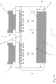
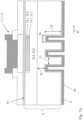
- Figure 1 shows a semiconductor switch element 10 comprising a first vertical transistor device 1.1 and a second vertical transistor device 1.2.
- the transistor devices 1.1, 1.2 are formed in the same substrate 8.
- a source region 2.1 of the first transistor device 1.1 and a source region 2.2 of the second transistor device 1.2 are arranged.
- a drain region 4.1 of the first transistor device 1.1 and a drain region 4.2 of the second transistor device 1.2 are arranged.
- a conductive element 9 is formed on the second side 8.2 of the substrate 8. It electrically connects the drain region 4.1 of the first transistor device 1.1 and the drain region 4.2 of the second transistor device 1.2.
- a trench 11 extends vertically into the substrate 8, and a part 9.1 of the conductive element 9 is arranged in the trench 11.
- a vertical distance 23 between the conductive element 9 and a respective drift region 13.1, 13.2 of the respective transistor device 1.1, 1.2 can be reduced (e. g. to around 10 ⁇ m). In consequence, the electrical resistivity is reduced, see the description above in detail.
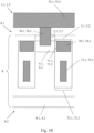
- Figure 1B shows an enlarged view of a transistor cell.
- the first and the second transistor 1.1, 1.2 have an identical layout, the following description applies for both of them.
- the body region 6.1, 6.2 is arranged.
- a gate region 5.1, 5.2 is formed, it comprises a gate electrode 70.1, 70.2 and a gate dielectric 71.1, 71.2.
- the gate region 5.1, 5.2 is arranged in a gate trench 72.1, 72.2.
- a field plate 73.1, 73.2 is formed in the gate trench 72.1, 72.2 below the gate electrode 70.1, 70.2, electrically isolated therefrom.
- the electrical contact of the gate electrode 70.1, 70.2 on the first side 8.1 of the substrate 8 is not visible (it is arranged in front of or behind the drawing plane).
- the source region 2.1, 2.2 and the body region 6.1, 6.2 are shorted, they can be contacted via a contact pad 75.1, 75.2 formed on the first side 8.1 of the substrate 8.
- a contact plug 76.1, 76.2 connects the contact pad 75.1, 75.2 to the source and body region 2.1, 2.2, 6.1, 6.2.
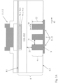
- Figure 2A shows the switch element 10 of figure 1A in another sectional plane, perpendicular to the sectional plane of figure 1A . Comparing the different views of figures 1A and 2A , it can be seen that three trenches 11 are formed in the substrate 8.
- the trenches 11 are longitudinal trenches 21 which extend in a first vertical direction 41 from the first transistor device 1.1 to the second transistor device 1.2 ( figure 1A ).
- the trenches 11, 21 are arranged laterally aside each other ( figure 2A ).
- the trenches 11, 21 respectively have a lateral width 30 of around 30 ⁇ m.
- a lateral distance 31 in between the trenches 11, 21 is around 30 ⁇ m in this example.
- the trenches 11, 21 have a depth 22 of around 35 ⁇ m.
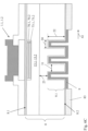
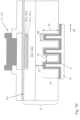
- figure 2B differs from figure 2A in that the conductive material of the conductive element 9 fills only a respective portion 11.1 of a respective trench 11. In another portion 11.2 of the respective trench 11, no conductive material is arranged. Likewise, more space to relax is left for the conductive material, e. g. metal, which can reduce the mechanical stress in the substrate 8.
- the conductive material e. g. metal
- the embodiment of figure 3 differs from figure 2B in that the other portion 11.2 of the respective trench 11 is filled up with a polymeric material 35.
- the polymeric material 35 can for instance be an epoxy resin, it covers the second side 8.2 of the substrate 8 partly. It can provide a protection against humidity and the like.
- Figure 4 shows a schematic top view of a switch element 10 comprising a first transistor device 1.1 and a second transistor device 1.2 formed in the same substrate 8.
- the first and the second transistor device 1.1, 1.2 are connected by a conductive element (not shown in figure 4 ).
- the conductive element is arranged in trenches 11, namely hole-shaped trenches 51 in this embodiment.
- the hole-shaped trenches 51 can have the same design as the trenches 11 shown in figures 2A , 2B and 3 . They can be filled entirely or partly with the conductive material, optionally in combination with a polymeric material.
- the hole-shaped trenches are arranged in rows 55. Therein, the hole-shaped trenches of neighbouring rows 55.1, 55.2 are arranged with an offset 56 to each other. Likewise, the packing density of the hole-shaped trenches 51 can be increased without reducing the minimum distance between neighbouring hole-shaped trenches 51.
- FIG. 5 shows a switch device 60 comprising a switch element 10 as described above and a board 61.
- the switch element 10 is mounted on the board 61 by flip chip bonding, the first side 8.1 of the substrate 8 faces the board 61.
- the electrical contact to the board 61 is formed via the contact pads 75.1, 75.2, these are soldered directly to the board 61 (not shown in detail).
- Figures 6A-D illustrate some manufacturing steps for the switch element 10 of figure 2B .
- a hard mask 80 is deposited on the second side 8.2 of the substrate 8 and structured.
- the hard mask 8 defines the locations 81 where the trenches 11 are etched.
- a seed layer 82 is deposited ( figure 6B ), for instance by sputtering.
- a photoresist mask 83 is deposited and structured.
- the photoresist mask 83 defines the location for the metal deposition in the subsequent plating process ( figure 6C ), for instance copper plating.
- the photoresist mask 83 is removed, leaving the conductive element 9 formed in the plating process.
- the part of the seed layer 82 aside the conductive element 9 can be removed in a brief etch step.
- Figures 7A-D illustrate some manufacturing steps for the switch element 10 of figure 3 .
- the metal plating is applied without a photoresist mask
- the conductive material 90 covers the entire second side 8.2 of the substrate 8 ( figure 7A ).
- the polymeric material 35 is deposited, filling the remaining holes in the trenches 11 ( figure 7B ).
- the polymeric material 35 is structured ( figure 7C ) and used as a mask for the removal of the conductive material 90 arranged laterally at the side ( figure 7D ). polymeric material 35 remains in the trenches 11.
- Figure 8 illustrates some manufacturing steps in a flow diagram 95. After forming 91 the transistor devices 1.1, 1.2, the trench 11 is etched 92 into the substrate 8. Thereafter, the trench 11 is filled 93 partly with the conductive material to form the conductive element 9.
Landscapes
- Metal-Oxide And Bipolar Metal-Oxide Semiconductor Integrated Circuits (AREA)
- Electrodes Of Semiconductors (AREA)
Claims (13)
- Halbleiterschaltelement (10), umfassendeine erste vertikale Transistorvorrichtung (1.1), die in einem Substrat (8) ausgebildet ist, miteinem Source-Bereich (2.1), der auf einer ersten Seite (8.1) des Substrats (8) ausgebildet ist, undeinem Drain-Bereich (4.1), der auf einer zweiten Seite (8.2) des Substrats (8) ausgebildet ist, die der ersten Seite (8.1) vertikal entgegengesetzt liegt,eine zweite vertikale Transistorvorrichtung (1.2), die seitlich neben der ersten vertikalen Transistorvorrichtung (1.1) in demselben Substrat (8) ausgebildet ist, miteinem Source-Bereich (2.2), der auf der ersten Seite (8.1) des Substrats (8) ausgebildet ist, undeinem Drain-Bereich (4.2), der auf der zweiten Seite (8.2) des Substrats (8) ausgebildet ist,ein leitfähiges Element (9), das auf der zweiten Seite (8.2) des Substrats (8) angeordnet ist und die Drain-Bereiche (4.1, 4.2) der vertikalen Transistorvorrichtungen (1.1, 1.2) elektrisch verbindet,wobei ein Graben (11), der sich vertikal in das Substrat (8) erstreckt, auf der zweiten Seite (8.2) des Substrats (8) ausgebildet ist,und wobei zumindest ein Teil (9.1) des leitfähigen Elements (9) in dem Graben (11) angeordnet ist,wobei ein leitfähiges Material, aus dem das leitfähige Element (9) ausgebildet ist, nur einen Abschnitt (11.1) des Grabens (11) füllt,dadurch gekennzeichnet, dass ein anderer Abschnitt (11.2) des Grabens (11) mit einem Polymermaterial (35) gefüllt ist,wobei das Polymermaterial die zweite Seite (8.2) des Substrats (8) nur teilweise bedeckt.
- Halbleiterschaltelement (10) nach Anspruch 1, wobei der Graben (11) eine vertikale Tiefe (22) von mindestens 15 µm und höchstens 40 µm aufweist.
- Halbleiterschaltelement (10) nach Anspruch 1 oder 2, wobei ein vertikaler Abstand (23) zwischen einem Boden (15) des Grabens (11) und einem jeweiligen Driftbereich (13.1, 13.2) der jeweiligen Transistorvorrichtung (1.1, 1.2) höchstens 30 µm beträgt.
- Halbleiterschaltelement (10) nach einem der vorhergehenden Ansprüche, wobei der Graben (11) eine laterale Breite (30) von höchstens 100 µm aufweist.
- Halbleiterschaltelement (10) nach einem der vorhergehenden Ansprüche, wobei eine Vielzahl von Gräben (11), die sich jeweils vertikal in das Substrat (8) erstrecken, auf der zweiten Seite (8.2) des Substrats (8) ausgebildet sind, wobei zumindest ein Teil (9.1) des leitfähigen Elements (9) jeweils in jedem Graben (11) der Vielzahl von Gräben (11) angeordnet ist.
- Halbleiterschaltelement (10) nach Anspruch 5, wobei die vertikalen Transistorvorrichtungen (1.1, 1.2) seitlich nebeneinander in einer ersten lateralen Richtung (41) angeordnet sind, wobei zumindest einige der Gräben (11) seitlich nebeneinander in einer zweiten lateralen Richtung (42) senkrecht zu der ersten lateralen Richtung (41) angeordnet sind.
- Halbleiterschaltelement (10) nach Anspruch 5 oder 6, wobei die Gräben (11) lochförmige Gräben (51) sind, wobei eine erste Teilmenge (51.1) der lochförmigen Gräben vertikal ausgerichtet mit der ersten Transistorvorrichtung (1.1) angeordnet ist und eine zweite Teilmenge (51.2) der lochförmigen Gräben (51) vertikal ausgerichtet mit der zweiten Transistorvorrichtung (1.2) angeordnet ist.
- Halbleiterschaltelement (10) nach einem der Ansprüche 5 bis 7, wobei die Gräben (11) lochförmige Gräben (51) sind, die in Reihen (55) angeordnet sind, wobei die lochförmigen Gräben (51) benachbarter Reihen (55.1, 55.2) mit einem Versatz (56) zueinander angeordnet sind.
- Halbleiterschaltelement (10) nach einem der Ansprüche 5 bis 8, wobei die Gräben (11) lochförmige Gräben (51) mit einem kreisförmigen Querschnitt in einer lateralen Ebene sind.
- Halbleiterschaltelement (10) nach einem der Ansprüche 1 bis 6, wobei der Graben (11) oder die Gräben (11) ein Längsgraben (21) ist oder Längsgräben (21) sind, der bzw. die sich seitlich von der ersten vertikalen Transistorvorrichtung (1.1) zu der zweiten vertikalen Transistorvorrichtung (1.2) erstreckt bzw. erstrecken.
- Schaltvorrichtung, umfassendein Halbleiterschaltelement (10) nach einem der vorhergehenden Ansprüche, und eine Platine, auf der das Halbleiterschaltelement (10) montiert ist,wobei das Halbleiterschaltelement (10) durch Flip-Chip-Bonden auf der Platine montiert ist, wobei die erste Seite (8.1) des Substrats (8) der Platine zugewandt ist.
- Verfahren zum Herstellen eines Halbleiterschaltelements (10) nach einem der Ansprüche 1-10, wobei das Verfahren die Schritte umfasst:i) Ausbilden der Transistorvorrichtungen (1.1, 1.2);ii) Ätzen des Grabens (11) in das Substrat (8), und zwar auf der zweiten Seite (8.2) des Substrats (8);iii) teilweises Füllen des Grabens (11) mit einem leitfähigen Material, um das leitfähige Element (9) auszubilden.
- Verwendung eines Halbleiterschaltelements (10) nach einem der Ansprüche 1-10 oder einer Schaltvorrichtung nach Anspruch 11 in einem Batteriemanagementsystem, insbesondere zum Verbinden und Trennen einer Batterie mit einem Lade- und/oder Entladepfad.
Priority Applications (4)
| Application Number | Priority Date | Filing Date | Title |
|---|---|---|---|
| EP19215271.8A EP3836201B1 (de) | 2019-12-11 | 2019-12-11 | Halbleiterschaltelement und verfahren zur herstellung davon |
| KR1020200172097A KR20210075019A (ko) | 2019-12-11 | 2020-12-10 | 반도체 스위치 소자 및 그 제조 방법 |
| US17/117,576 US11581369B2 (en) | 2019-12-11 | 2020-12-10 | Semiconductor switch element and method of manufacturing the same |
| CN202011444549.1A CN112951903A (zh) | 2019-12-11 | 2020-12-11 | 半导体开关元件及其制造方法 |
Applications Claiming Priority (1)
| Application Number | Priority Date | Filing Date | Title |
|---|---|---|---|
| EP19215271.8A EP3836201B1 (de) | 2019-12-11 | 2019-12-11 | Halbleiterschaltelement und verfahren zur herstellung davon |
Publications (2)
| Publication Number | Publication Date |
|---|---|
| EP3836201A1 EP3836201A1 (de) | 2021-06-16 |
| EP3836201B1 true EP3836201B1 (de) | 2025-04-23 |
Family
ID=68886854
Family Applications (1)
| Application Number | Title | Priority Date | Filing Date |
|---|---|---|---|
| EP19215271.8A Active EP3836201B1 (de) | 2019-12-11 | 2019-12-11 | Halbleiterschaltelement und verfahren zur herstellung davon |
Country Status (4)
| Country | Link |
|---|---|
| US (1) | US11581369B2 (de) |
| EP (1) | EP3836201B1 (de) |
| KR (1) | KR20210075019A (de) |
| CN (1) | CN112951903A (de) |
Families Citing this family (3)
| Publication number | Priority date | Publication date | Assignee | Title |
|---|---|---|---|---|
| WO2022210367A1 (ja) * | 2021-03-29 | 2022-10-06 | ヌヴォトンテクノロジージャパン株式会社 | 半導体装置、電池保護回路、および、パワーマネージメント回路 |
| DE102022128515B3 (de) * | 2022-10-27 | 2024-02-15 | Infineon Technologies Ag | Sic-halbleiterkörper enthaltende vertikale leistungs-halbleitervorrichtung |
| CN118943166A (zh) * | 2024-07-26 | 2024-11-12 | 深圳市创飞芯源半导体有限公司 | 共漏极mosfet器件及制备方法、电子设备及制备方法 |
Family Cites Families (10)
| Publication number | Priority date | Publication date | Assignee | Title |
|---|---|---|---|---|
| JP4015504B2 (ja) * | 2002-08-09 | 2007-11-28 | 株式会社ルネサステクノロジ | 半導体装置 |
| CN202231176U (zh) * | 2008-09-30 | 2012-05-23 | 苹果公司 | 尺寸减小的多引脚阴性插座连接器 |
| JP2010087096A (ja) * | 2008-09-30 | 2010-04-15 | Sanyo Electric Co Ltd | 半導体装置及びその製造方法 |
| JP2010103208A (ja) * | 2008-10-22 | 2010-05-06 | Denso Corp | 半導体装置 |
| US20100103208A1 (en) * | 2008-10-28 | 2010-04-29 | Olympus Corporation | Ink filling method and inkjet printer |
| US8058732B2 (en) * | 2008-11-20 | 2011-11-15 | Fairchild Semiconductor Corporation | Semiconductor die structures for wafer-level chipscale packaging of power devices, packages and systems for using the same, and methods of making the same |
| JP5995435B2 (ja) * | 2011-08-02 | 2016-09-21 | ローム株式会社 | 半導体装置およびその製造方法 |
| JP2015231033A (ja) * | 2014-06-06 | 2015-12-21 | ルネサスエレクトロニクス株式会社 | 半導体装置及び半導体装置の製造方法 |
| JP2018049974A (ja) * | 2016-09-23 | 2018-03-29 | ルネサスエレクトロニクス株式会社 | 半導体装置およびその製造方法 |
| CN108962997A (zh) * | 2018-07-25 | 2018-12-07 | 阳林涛 | 一种功率器件及其制作方法 |
-
2019
- 2019-12-11 EP EP19215271.8A patent/EP3836201B1/de active Active
-
2020
- 2020-12-10 US US17/117,576 patent/US11581369B2/en active Active
- 2020-12-10 KR KR1020200172097A patent/KR20210075019A/ko not_active Ceased
- 2020-12-11 CN CN202011444549.1A patent/CN112951903A/zh active Pending
Also Published As
| Publication number | Publication date |
|---|---|
| KR20210075019A (ko) | 2021-06-22 |
| CN112951903A (zh) | 2021-06-11 |
| US11581369B2 (en) | 2023-02-14 |
| US20210183948A1 (en) | 2021-06-17 |
| EP3836201A1 (de) | 2021-06-16 |
Similar Documents
| Publication | Publication Date | Title |
|---|---|---|
| US10388781B2 (en) | Device structure having inter-digitated back to back MOSFETs | |
| JP4646284B2 (ja) | 単一表面上のバンプコンタクトを有する垂直伝導フリップチップ半導体デバイス | |
| US9576841B2 (en) | Semiconductor device and manufacturing method | |
| US11581369B2 (en) | Semiconductor switch element and method of manufacturing the same | |
| US8324686B2 (en) | Semiconductor device and method for manufacturing | |
| US20130168832A1 (en) | Semiconductor device | |
| EP0091079A2 (de) | Leistungs-MOSFET | |
| US5592026A (en) | Integrated structure pad assembly for lead bonding | |
| US9899343B2 (en) | High voltage tolerant bonding pad structure for trench-based semiconductor devices | |
| WO2022192830A1 (en) | Vertical transistors with gate connection grid | |
| CN114496987B (zh) | Mosfet功率器件及其形成方法、csp封装模块 | |
| US20260143687A1 (en) | Semiconductor devices | |
| EP4718989A1 (de) | Halbleiterchip mit vertikaler transistorvorrichtung | |
| US20240203835A1 (en) | Semiconductor device | |
| US20250125308A1 (en) | Semiconductor circuit device | |
| EP4156279A1 (de) | Halbleiterchip und verfahren zur herstellung davon | |
| EP4561291A1 (de) | Graben-halbleiterleistungsbauelement | |
| WO2023223589A1 (ja) | 半導体チップ | |
| CN121924798A (zh) | 半导体器件 | |
| WO2023223590A1 (ja) | 半導体チップ | |
| US20050269711A1 (en) | Semiconductor device | |
| KR20260038481A (ko) | 반도체 장치 | |
| CN118658858A (zh) | 具有垂直器件的半导体管芯 | |
| CN117954314A (zh) | 半导体封装结构及其制造方法 |
Legal Events
| Date | Code | Title | Description |
|---|---|---|---|
| PUAI | Public reference made under article 153(3) epc to a published international application that has entered the european phase |
Free format text: ORIGINAL CODE: 0009012 |
|
| STAA | Information on the status of an ep patent application or granted ep patent |
Free format text: STATUS: THE APPLICATION HAS BEEN PUBLISHED |
|
| AK | Designated contracting states |
Kind code of ref document: A1 Designated state(s): AL AT BE BG CH CY CZ DE DK EE ES FI FR GB GR HR HU IE IS IT LI LT LU LV MC MK MT NL NO PL PT RO RS SE SI SK SM TR |
|
| STAA | Information on the status of an ep patent application or granted ep patent |
Free format text: STATUS: REQUEST FOR EXAMINATION WAS MADE |
|
| 17P | Request for examination filed |
Effective date: 20211215 |
|
| RBV | Designated contracting states (corrected) |
Designated state(s): AL AT BE BG CH CY CZ DE DK EE ES FI FR GB GR HR HU IE IS IT LI LT LU LV MC MK MT NL NO PL PT RO RS SE SI SK SM TR |
|
| REG | Reference to a national code |
Ref country code: DE Ref legal event code: R079 Free format text: PREVIOUS MAIN CLASS: H01L0021823400 Ipc: H10D0084010000 Ref country code: DE Ref legal event code: R079 Ref document number: 602019068945 Country of ref document: DE Free format text: PREVIOUS MAIN CLASS: H01L0021823400 Ipc: H10D0084010000 |
|
| GRAP | Despatch of communication of intention to grant a patent |
Free format text: ORIGINAL CODE: EPIDOSNIGR1 |
|
| STAA | Information on the status of an ep patent application or granted ep patent |
Free format text: STATUS: GRANT OF PATENT IS INTENDED |
|
| RIC1 | Information provided on ipc code assigned before grant |
Ipc: H10D 84/03 20250101ALI20250204BHEP Ipc: H10D 64/00 20250101ALI20250204BHEP Ipc: H10D 30/66 20250101ALI20250204BHEP Ipc: H10D 84/83 20250101ALI20250204BHEP Ipc: H10D 84/01 20250101AFI20250204BHEP |
|
| GRAS | Grant fee paid |
Free format text: ORIGINAL CODE: EPIDOSNIGR3 |
|
| GRAA | (expected) grant |
Free format text: ORIGINAL CODE: 0009210 |
|
| STAA | Information on the status of an ep patent application or granted ep patent |
Free format text: STATUS: THE PATENT HAS BEEN GRANTED |
|
| INTG | Intention to grant announced |
Effective date: 20250221 |
|
| AK | Designated contracting states |
Kind code of ref document: B1 Designated state(s): AL AT BE BG CH CY CZ DE DK EE ES FI FR GB GR HR HU IE IS IT LI LT LU LV MC MK MT NL NO PL PT RO RS SE SI SK SM TR |
|
| REG | Reference to a national code |
Ref country code: GB Ref legal event code: FG4D |
|
| REG | Reference to a national code |
Ref country code: CH Ref legal event code: EP |
|
| REG | Reference to a national code |
Ref country code: DE Ref legal event code: R096 Ref document number: 602019068945 Country of ref document: DE |
|
| REG | Reference to a national code |
Ref country code: IE Ref legal event code: FG4D |
|
| P01 | Opt-out of the competence of the unified patent court (upc) registered |
Free format text: CASE NUMBER: APP_20507/2025 Effective date: 20250429 |
|
| REG | Reference to a national code |
Ref country code: NL Ref legal event code: MP Effective date: 20250423 |
|
| PG25 | Lapsed in a contracting state [announced via postgrant information from national office to epo] |
Ref country code: NL Free format text: LAPSE BECAUSE OF FAILURE TO SUBMIT A TRANSLATION OF THE DESCRIPTION OR TO PAY THE FEE WITHIN THE PRESCRIBED TIME-LIMIT Effective date: 20250423 |
|
| REG | Reference to a national code |
Ref country code: AT Ref legal event code: MK05 Ref document number: 1789111 Country of ref document: AT Kind code of ref document: T Effective date: 20250423 |
|
| PG25 | Lapsed in a contracting state [announced via postgrant information from national office to epo] |
Ref country code: PT Free format text: LAPSE BECAUSE OF FAILURE TO SUBMIT A TRANSLATION OF THE DESCRIPTION OR TO PAY THE FEE WITHIN THE PRESCRIBED TIME-LIMIT Effective date: 20250825 Ref country code: FI Free format text: LAPSE BECAUSE OF FAILURE TO SUBMIT A TRANSLATION OF THE DESCRIPTION OR TO PAY THE FEE WITHIN THE PRESCRIBED TIME-LIMIT Effective date: 20250423 Ref country code: ES Free format text: LAPSE BECAUSE OF FAILURE TO SUBMIT A TRANSLATION OF THE DESCRIPTION OR TO PAY THE FEE WITHIN THE PRESCRIBED TIME-LIMIT Effective date: 20250423 |
|
| REG | Reference to a national code |
Ref country code: LT Ref legal event code: MG9D |
|
| PG25 | Lapsed in a contracting state [announced via postgrant information from national office to epo] |
Ref country code: GR Free format text: LAPSE BECAUSE OF FAILURE TO SUBMIT A TRANSLATION OF THE DESCRIPTION OR TO PAY THE FEE WITHIN THE PRESCRIBED TIME-LIMIT Effective date: 20250724 Ref country code: NO Free format text: LAPSE BECAUSE OF FAILURE TO SUBMIT A TRANSLATION OF THE DESCRIPTION OR TO PAY THE FEE WITHIN THE PRESCRIBED TIME-LIMIT Effective date: 20250723 |
|
| PG25 | Lapsed in a contracting state [announced via postgrant information from national office to epo] |
Ref country code: PL Free format text: LAPSE BECAUSE OF FAILURE TO SUBMIT A TRANSLATION OF THE DESCRIPTION OR TO PAY THE FEE WITHIN THE PRESCRIBED TIME-LIMIT Effective date: 20250423 |
|
| PG25 | Lapsed in a contracting state [announced via postgrant information from national office to epo] |
Ref country code: BG Free format text: LAPSE BECAUSE OF FAILURE TO SUBMIT A TRANSLATION OF THE DESCRIPTION OR TO PAY THE FEE WITHIN THE PRESCRIBED TIME-LIMIT Effective date: 20250423 |
|
| PG25 | Lapsed in a contracting state [announced via postgrant information from national office to epo] |
Ref country code: HR Free format text: LAPSE BECAUSE OF FAILURE TO SUBMIT A TRANSLATION OF THE DESCRIPTION OR TO PAY THE FEE WITHIN THE PRESCRIBED TIME-LIMIT Effective date: 20250423 |
|
| PG25 | Lapsed in a contracting state [announced via postgrant information from national office to epo] |
Ref country code: AT Free format text: LAPSE BECAUSE OF FAILURE TO SUBMIT A TRANSLATION OF THE DESCRIPTION OR TO PAY THE FEE WITHIN THE PRESCRIBED TIME-LIMIT Effective date: 20250423 |
|
| PG25 | Lapsed in a contracting state [announced via postgrant information from national office to epo] |
Ref country code: RS Free format text: LAPSE BECAUSE OF FAILURE TO SUBMIT A TRANSLATION OF THE DESCRIPTION OR TO PAY THE FEE WITHIN THE PRESCRIBED TIME-LIMIT Effective date: 20250723 |
|
| PG25 | Lapsed in a contracting state [announced via postgrant information from national office to epo] |
Ref country code: IS Free format text: LAPSE BECAUSE OF FAILURE TO SUBMIT A TRANSLATION OF THE DESCRIPTION OR TO PAY THE FEE WITHIN THE PRESCRIBED TIME-LIMIT Effective date: 20250823 |
|
| PG25 | Lapsed in a contracting state [announced via postgrant information from national office to epo] |
Ref country code: LV Free format text: LAPSE BECAUSE OF FAILURE TO SUBMIT A TRANSLATION OF THE DESCRIPTION OR TO PAY THE FEE WITHIN THE PRESCRIBED TIME-LIMIT Effective date: 20250423 |
|
| PG25 | Lapsed in a contracting state [announced via postgrant information from national office to epo] |
Ref country code: DK Free format text: LAPSE BECAUSE OF FAILURE TO SUBMIT A TRANSLATION OF THE DESCRIPTION OR TO PAY THE FEE WITHIN THE PRESCRIBED TIME-LIMIT Effective date: 20250423 Ref country code: SM Free format text: LAPSE BECAUSE OF FAILURE TO SUBMIT A TRANSLATION OF THE DESCRIPTION OR TO PAY THE FEE WITHIN THE PRESCRIBED TIME-LIMIT Effective date: 20250423 |
|
| PG25 | Lapsed in a contracting state [announced via postgrant information from national office to epo] |
Ref country code: CZ Free format text: LAPSE BECAUSE OF FAILURE TO SUBMIT A TRANSLATION OF THE DESCRIPTION OR TO PAY THE FEE WITHIN THE PRESCRIBED TIME-LIMIT Effective date: 20250423 |
|
| PG25 | Lapsed in a contracting state [announced via postgrant information from national office to epo] |
Ref country code: EE Free format text: LAPSE BECAUSE OF FAILURE TO SUBMIT A TRANSLATION OF THE DESCRIPTION OR TO PAY THE FEE WITHIN THE PRESCRIBED TIME-LIMIT Effective date: 20250423 |
|
| REG | Reference to a national code |
Ref country code: DE Ref legal event code: R097 Ref document number: 602019068945 Country of ref document: DE |
|
| PG25 | Lapsed in a contracting state [announced via postgrant information from national office to epo] |
Ref country code: RO Free format text: LAPSE BECAUSE OF FAILURE TO SUBMIT A TRANSLATION OF THE DESCRIPTION OR TO PAY THE FEE WITHIN THE PRESCRIBED TIME-LIMIT Effective date: 20250423 Ref country code: SK Free format text: LAPSE BECAUSE OF FAILURE TO SUBMIT A TRANSLATION OF THE DESCRIPTION OR TO PAY THE FEE WITHIN THE PRESCRIBED TIME-LIMIT Effective date: 20250423 |
|
| PG25 | Lapsed in a contracting state [announced via postgrant information from national office to epo] |
Ref country code: IT Free format text: LAPSE BECAUSE OF FAILURE TO SUBMIT A TRANSLATION OF THE DESCRIPTION OR TO PAY THE FEE WITHIN THE PRESCRIBED TIME-LIMIT Effective date: 20250423 |
|
| PLBE | No opposition filed within time limit |
Free format text: ORIGINAL CODE: 0009261 |
|
| STAA | Information on the status of an ep patent application or granted ep patent |
Free format text: STATUS: NO OPPOSITION FILED WITHIN TIME LIMIT |
|
| REG | Reference to a national code |
Ref country code: CH Ref legal event code: L10 Free format text: ST27 STATUS EVENT CODE: U-0-0-L10-L00 (AS PROVIDED BY THE NATIONAL OFFICE) Effective date: 20260304 |
|
| 26N | No opposition filed |
Effective date: 20260126 |
|
| PGFP | Annual fee paid to national office [announced via postgrant information from national office to epo] |
Ref country code: DE Payment date: 20260224 Year of fee payment: 7 |