EP3813137B1 - Display device - Google Patents
Display device Download PDFInfo
- Publication number
- EP3813137B1 EP3813137B1 EP19837592.5A EP19837592A EP3813137B1 EP 3813137 B1 EP3813137 B1 EP 3813137B1 EP 19837592 A EP19837592 A EP 19837592A EP 3813137 B1 EP3813137 B1 EP 3813137B1
- Authority
- EP
- European Patent Office
- Prior art keywords
- data
- line
- display area
- area
- display apparatus
- Prior art date
- Legal status (The legal status is an assumption and is not a legal conclusion. Google has not performed a legal analysis and makes no representation as to the accuracy of the status listed.)
- Active
Links
Images


Classifications
-
- H—ELECTRICITY
- H10—SEMICONDUCTOR DEVICES; ELECTRIC SOLID-STATE DEVICES NOT OTHERWISE PROVIDED FOR
- H10K—ORGANIC ELECTRIC SOLID-STATE DEVICES
- H10K59/00—Integrated devices, or assemblies of multiple devices, comprising at least one organic light-emitting element covered by group H10K50/00
- H10K59/10—OLED displays
- H10K59/12—Active-matrix OLED [AMOLED] displays
- H10K59/131—Interconnections, e.g. wiring lines or terminals
- H10K59/1315—Interconnections, e.g. wiring lines or terminals comprising structures specially adapted for lowering the resistance
-
- H—ELECTRICITY
- H10—SEMICONDUCTOR DEVICES; ELECTRIC SOLID-STATE DEVICES NOT OTHERWISE PROVIDED FOR
- H10K—ORGANIC ELECTRIC SOLID-STATE DEVICES
- H10K50/00—Organic light-emitting devices
- H10K50/80—Constructional details
-
- H—ELECTRICITY
- H10—SEMICONDUCTOR DEVICES; ELECTRIC SOLID-STATE DEVICES NOT OTHERWISE PROVIDED FOR
- H10K—ORGANIC ELECTRIC SOLID-STATE DEVICES
- H10K59/00—Integrated devices, or assemblies of multiple devices, comprising at least one organic light-emitting element covered by group H10K50/00
- H10K59/10—OLED displays
- H10K59/12—Active-matrix OLED [AMOLED] displays
- H10K59/121—Active-matrix OLED [AMOLED] displays characterised by the geometry or disposition of pixel elements
- H10K59/1213—Active-matrix OLED [AMOLED] displays characterised by the geometry or disposition of pixel elements the pixel elements being TFTs
-
- H—ELECTRICITY
- H10—SEMICONDUCTOR DEVICES; ELECTRIC SOLID-STATE DEVICES NOT OTHERWISE PROVIDED FOR
- H10K—ORGANIC ELECTRIC SOLID-STATE DEVICES
- H10K59/00—Integrated devices, or assemblies of multiple devices, comprising at least one organic light-emitting element covered by group H10K50/00
- H10K59/10—OLED displays
- H10K59/12—Active-matrix OLED [AMOLED] displays
- H10K59/126—Shielding, e.g. light-blocking means over the TFTs
-
- H—ELECTRICITY
- H10—SEMICONDUCTOR DEVICES; ELECTRIC SOLID-STATE DEVICES NOT OTHERWISE PROVIDED FOR
- H10K—ORGANIC ELECTRIC SOLID-STATE DEVICES
- H10K77/00—Constructional details of devices covered by this subclass and not covered by groups H10K10/80, H10K30/80, H10K50/80 or H10K59/80
- H10K77/10—Substrates, e.g. flexible substrates
- H10K77/111—Flexible substrates
-
- H—ELECTRICITY
- H10—SEMICONDUCTOR DEVICES; ELECTRIC SOLID-STATE DEVICES NOT OTHERWISE PROVIDED FOR
- H10K—ORGANIC ELECTRIC SOLID-STATE DEVICES
- H10K2102/00—Constructional details relating to the organic devices covered by this subclass
- H10K2102/301—Details of OLEDs
- H10K2102/302—Details of OLEDs of OLED structures
- H10K2102/3023—Direction of light emission
-
- H—ELECTRICITY
- H10—SEMICONDUCTOR DEVICES; ELECTRIC SOLID-STATE DEVICES NOT OTHERWISE PROVIDED FOR
- H10K—ORGANIC ELECTRIC SOLID-STATE DEVICES
- H10K2102/00—Constructional details relating to the organic devices covered by this subclass
- H10K2102/301—Details of OLEDs
- H10K2102/311—Flexible OLED
-
- Y—GENERAL TAGGING OF NEW TECHNOLOGICAL DEVELOPMENTS; GENERAL TAGGING OF CROSS-SECTIONAL TECHNOLOGIES SPANNING OVER SEVERAL SECTIONS OF THE IPC; TECHNICAL SUBJECTS COVERED BY FORMER USPC CROSS-REFERENCE ART COLLECTIONS [XRACs] AND DIGESTS
- Y02—TECHNOLOGIES OR APPLICATIONS FOR MITIGATION OR ADAPTATION AGAINST CLIMATE CHANGE
- Y02E—REDUCTION OF GREENHOUSE GAS [GHG] EMISSIONS, RELATED TO ENERGY GENERATION, TRANSMISSION OR DISTRIBUTION
- Y02E10/00—Energy generation through renewable energy sources
- Y02E10/50—Photovoltaic [PV] energy
- Y02E10/549—Organic PV cells
Definitions
- Embodiments relate generally to a display apparatus. More particularly, embodiments of the present disclosure relate to a display apparatus in which a width of a peripheral area that is a non-display area is reduced.
- CTR cathode ray tube
- the display apparatus includes a display area for displaying an image, and a peripheral area that is a non-display area around the display area. In this case, efforts have been made to reduce a width of the peripheral area.
- GB 2420651 A discloses a display device having data link lines connecting data lines to a data pad.
- US 2018/130856 A1 discloses a display device having connection lines in a non-display area connecting data lines to a data pad.
- WO2018/062023 A1 discloses a display panel having connection lines in the display area connecting data lines to a data pad.
- Embodiments provide a display apparatus in which a width of a peripheral area that is a non-display area is reduced.
- the first connecting line is disposed in the display area other than the peripheral area, a display apparatus in which a width of the peripheral area is reduced to reduce a bezel portion, which is a non-display area, can be implemented.
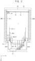
- FIG. 1 is a plan view showing a display apparatus according to embodiments.
- a display apparatus includes a display area AA for displaying an image, and a peripheral area PA that is a non-display area adjacent to the display area AA and surrounding the display area AA.
- the display area AA may have a rectangular shape on a plane defined by a first direction D1 and a second direction D2 perpendicular to the first direction D1, and a corner of the display area AA may have a round shape.
- the display area AA may have a rectangular shape including rounded corners, but embodiments are not limited thereto.
- the peripheral area PA may include: a left peripheral area adjacent to a left side of the display area AA; a right peripheral area adjacent to a right side of the display area AA; an upper peripheral area adjacent to an upper side of the display area AA; and a lower peripheral area adjacent to a lower side of the display area AA.
- a data pad COP and a gate pad FOP for connecting a driver may be disposed in the lower peripheral area, so that the lower peripheral area may have a width greater than a width of each of the upper, left, and right peripheral areas.
- the lower peripheral area may include: a first peripheral area PAa directly adjacent to the display area AA; a bending area BA; and a second peripheral area PAb.
- the data pad COP and the gate pad FOP may be disposed in the second peripheral area PAb.
- the bending area BA may be a portion folded to place the second peripheral area PAb on a rear surface of the display apparatus, and the bending area BA may be disposed between the first peripheral area PAa and the second peripheral area PAb.
- a length of the bending area BA in the first direction D1 may be smaller than a length of the display area AA in the first direction D1. Accordingly, data lines, which are located outward in the first direction D1 compared to a data spider line DSPL disposed in the lower peripheral area, are connected to the data spider line DSPL through a connecting line CL.
- the data spider line DSPL may be electrically connected to a data line disposed in the display area AA and to the data pad COP. Meanwhile, a gate spider line GSPL connected to a scan driver or a data driver and connected to the gate pad FOP may be disposed at a portion adjacent to the data spider line DSPL in the lower peripheral area.
- a chip including the data driver may be connected to the data pad COP.
- a driving substrate including a timing controller may be connected to the gate pad FOP.
- FIG. 2 is a block diagram illustrating an example of pixels and drivers included in the display apparatus of FIG. 1
- FIG. 3 is a diagram illustrating an example of a pixel shown in FIG. 2
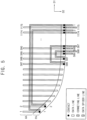
- FIG. 4 is an enlarged view showing a lower left portion of the display apparatus of FIG. 1
- FIG. 5 is a diagram for describing a connection relation between a data line and a connecting line of the display apparatus of FIG. 4 .
- the display apparatus may include a plurality of pixels PX, a driver, and a wire part.
- the driver may include a scan driver SDV, an emission driver EDV, a data driver DD, and a timing controller TC.
- positions of the scan driver SDV, the emission driver EDV, the data driver DD, and the timing controller TC are set for convenience of description, and the scan driver SDV, the emission driver EDV, the data driver DD, and the timing controller TC may be disposed at different positions in the display apparatus when implementing an actual display apparatus.
- the wire part may provide a signal of the driver to each pixel PX, and may include scan lines SL, data lines DL1, ..., DLn-1, DLn, DLn+1, ..., emission control lines EL, first and second power lines (not shown), and an initialization power line (not shown).
- Each pixel PX may be electrically connected to a scan line, a data line, and an emission control line.
- the pixels PX may receive data signals from the data lines DL1, ..., DLn-1, DLn, DLn+1, ....
- the pixels PX that have received the data signals may control an amount of a current flowing from a first power ELVDD to a second power ELVSS via an organic light emitting diode OLED.
- the data line is connected to the connecting line CL through a connection contact hole CCNT, and the connecting line CL may be connected to the data spider line DSPL through a spider contact hole SCNT; or the data line may be directly connected to the data spider line DSPL through the spider contact hole SCNT.
- n th data line DLn and the (n+1) th data line DLn+1 may be respectively directly connected to a corresponding data spider line DSPL through a corresponding spider contact hole SCNT in the peripheral area PA without passing through the connecting line.
- FIG. 5 conceptually shows a case where n is 589.
- each of the data spider lines DSPL1 and DSPL may extend in the second direction while being parallel to each other in the peripheral area PA between the bending area BA and the display area AA. Accordingly, compared to a conventional technology in which the data spider lines DSPL1 and DSPL are bent at a predetermined angle with respect to the second direction D2, a sufficient distance between the data spider lines DSPL1 and DSPL may be ensured, so that wire resistances of the data spider lines DSPL1 and DSPL may be reduced.
- the display apparatus includes a display area for displaying an image, and a peripheral area that is a non-display area surrounding the display area.
- the display apparatus includes: a base substrate; a first data line disposed in the display area on the base substrate and extending into the peripheral area in a second direction that is perpendicular to a first direction; a first connecting line at least partially disposed in the display area on the base substrate and electrically connected to the first data line through a connection contact hole in the peripheral area; a data pad disposed in the peripheral area; wherein the first connecting line includes a first portion extending in the second direction parallel to the first data line from the connection contact hole in the peripheral area into the display area, a second portion connected to the first portion in the display area and extending in the first direction within the display area and a third portion connected to the second portion, parallel to the first portion and extending from the display area into the peripheral area towards the data pad; the display apparatus further comprises a first data spider line disposed in the peripheral area between the data pad and the display area
- the scan driver SDV is disposed in the peripheral area PA adjacent to the left side of the display area AA
- the emission driver EDV is disposed in the peripheral area PA adjacent to the right side of the display area AA
- the scan driver and the emission driver connected to each other by the scan line, and the emission control line may be disposed in both the left and right peripheral areas, so that signals synchronized with each other may be supplied to the pixels from the left and right sides.
- the pixel PX may include an organic light emitting diode OLED, first to seventh transistors T1 to T7, and a storage capacitor CST.
- the organic light emitting diode OLED may include an anode connected to the first transistor T1 via the sixth transistor T6, and a cathode connected to the second power ELVSS.
- the organic light emitting diode OLED may generate light having a luminance in response to an amount of a current supplied from the first transistor T1.
- the first power ELVDD may be set as a voltage that is higher than a voltage of the second power ELVSS so that the current may flow through the organic light emitting diode OLED.
- the seventh transistor T7 may be connected between an initialization power VINT and the anode of the organic light emitting diode OLED.
- a gate electrode of the seventh transistor T7 may be connected to an (i+1) th -first scan line S1i+1 or an (i-1) th -first scan line S1i-1.
- the seventh transistor T7 may be turned on when a scan signal is supplied to the i th -first scan line S1i so that a voltage of the initialization power VINT may be supplied to the anode of the organic light emitting diode OLED.
- the initialization power VINT may be set as a voltage that is lower than a voltage of a data signal.
- the sixth transistor T6 may be connected between the first transistor T1 and the organic light emitting diode OLED.
- a gate electrode of the sixth transistor T6 may be connected to an i th -first emission control line E1i.
- the sixth transistor T6 may be turned off when an emission control signal is supplied to the i th -first emission control line E1i, and may be turned on in other cases.
- the fifth transistor T5 may be connected between the first power ELVDD and the first transistor T1.
- a gate electrode of the fifth transistor T5 may be connected to the i th -first emission control line E1i.
- the fifth transistor T5 may be turned off when the emission control signal is supplied to the i th -first emission control line E1i, and may be turned on in other cases.
- the first transistor T1 (a driving transistor) may include a first electrode connected to the first power ELVDD via the fifth transistor T5, and a second electrode connected to the anode of the organic light emitting diode OLED via the sixth transistor T6.
- a gate electrode of the first transistor T1 may be connected to a first node N1.
- the first transistor T1 may control an amount of a current flowing from the first power ELVDD to the second power ELVSS via the organic light emitting diode OLED in response to a voltage of the first node N1.
- the third transistor T3 may be connected between the second electrode of the first transistor T1 and the first node N1.
- a gate electrode of the third transistor T3 may be connected to the i th -first scan line S1i.
- the third transistor T3 may be turned on when the scan signal is supplied to the i th -first scan line S1i so that the second electrode of the first transistor T1 may be electrically connected to the first node N1. Accordingly, when the third transistor T3 is turned on, the first transistor T1 may be connected in the form of a diode.
- the fourth transistor T4 may be connected between the first node N1 and the initialization power VINT.
- a gate electrode of the fourth transistor T4 may be connected to the (i-1) th -first scan line S1i-1.
- the fourth transistor T4 may be turned on when the scan signal is supplied to the (i-1) th -first scan line S1i-1 so that the voltage of the initialization power VINT may be supplied to the first node N1.
- the second transistor T2 may be connected between the m th data line Dm and the first electrode of the first transistor T1.
- a gate electrode of the second transistor T2 may be connected to the i th -first scan line S1i.
- the second transistor T2 may be turned on when the scan signal is supplied to the i th -first scan line S1i so that the m th data line Dm may be electrically connected to the first electrode of the first transistor T1.
- the display apparatus may include a base substrate 100, a buffer layer 110, an active pattern ACT, a first gate insulating layer 120, a first gate pattern, a second gate insulating layer 130, a second gate pattern GAT2, an interlayer insulating layer 140, a first data pattern, a first insulating layer 160, a connecting line pattern, a second insulating layer 170, a pixel defining layer PDL, a light emitting structure 180, and a thin film encapsulation layer TFE.
- the base substrate 100 may include a transparent insulating substrate.
- the base substrate 100 may be a transparent resin substrate having flexibility.
- the transparent resin substrate may include a polyimide-based resin, an acryl-based resin, a polyacrylate-based resin, a polycarbonate-based resin, a polyether-based resin, a sulfonic acid-based resin, a polyethyleneterephthalate-based resin, and the like.
- the base substrate 100 may be a polyimide (PI) resin film.
- the buffer layer 110 may prevent metal atoms or impurities from diffusing from the base substrate 100, and may control a heat transfer rate during a crystallization process for forming the active pattern ACT, which will be described below, to obtain a substantially uniform active pattern ACT.
- the buffer layer 110 may serve to improve flatness of the surface of the base substrate 100.
- the buffer layer 110 may be formed by using a silicon compound such as silicon oxide (SiO x ), silicon nitride (SiN x ), silicon oxynitride (SiO x N y ), silicon oxycarbide (SiO x C y ), and silicon carbonitride (SiC x N y ).
- the buffer layer 110 may not be formed in the bending area BA of the peripheral area PA.
- the buffer layer 110 may not be formed in the bending area BA, or may be removed from the bending area BA. This is because the bending area BA is a portion that is folded in a final product, and when the buffer layer 110, which is an inorganic layer, is formed in the bending area BA, damage such as a crack may occur in the buffer layer 110.
- the insulating layers 120, 130, and the like, which are formed of an inorganic film may not be formed in the bending area BA.
- the active pattern ACT may be disposed on the buffer layer 110.
- the active pattern ACT may include active patterns ACT2 and ACT6 of thin film transistors TFT2 and TFT6 that are disposed in the display area AA to constitute a pixel structure, and an active pattern (not shown) disposed in the peripheral area PA to constitute a driving circuit.
- the driving circuit may be an amorphous silicon gate (ASG) circuit.
- the active patterns ACT2 and ACT6 of the thin film transistors TFT2 and TFT6 may include drain regions D2 and D6 and source regions S2 and S6, which are doped with impurities, and channel regions C2 and C6 disposed between the drain regions D2 and D6 and the source regions S2 and S6, respectively.
- the thin film transistors TFT2 and TFT6 may be the second transistor and the sixth transistor of FIG. 3 , respectively.
- the first gate pattern may be disposed on the first gate insulating layer 120.
- the first gate pattern may include: gate electrodes GE2 and GE6 of the thin film transistors TFT2 and TFT6; a signal line such as a gate line configured to transmit a signal for driving the pixel; and the like.
- the first gate pattern may be formed by using a metal, an alloy, metal nitride, conductive metal oxide, a transparent conductive material, and the like.
- the first gate pattern may be formed of a metal such as copper, aluminum, and molybdenum.
- the first gate pattern may have a layered structure including a plurality of layers.
- the first gate pattern may include a copper layer and a molybdenum layer disposed on the copper layer.
- the second gate pattern GAT2 may be disposed on the second gate insulating layer 130.
- the second gate pattern GAT2 may be formed by using a metal, an alloy, metal nitride, conductive metal oxide, a transparent conductive material, and the like.
- the second gate pattern GAT2 may be formed of a metal such as copper, aluminum, and molybdenum.
- the second gate pattern GAT2 may have a layered structure including a plurality of layers.
- the second gate pattern GAT2 may include a copper layer and a molybdenum layer disposed on the copper layer.
- the data spider line DSPL may include the first gate pattern and the second gate pattern that are alternately arranged.
- two adjacent data spider lines DSPL may be formed on different respective layers, so that a line width of each of the data spider lines DSPL may be increased. Accordingly, a width W for arranging one data spider line DSPL may be decreased.
- the interlayer insulating layer 140 may be disposed on the second gate insulating layer 130 on which the second gate pattern GAT2 is disposed.
- the first data pattern may be disposed on the interlayer insulating layer 140.
- the first data pattern may include the data line DL, a shielding electrode SH, and a first contact pad CP1.
- the first data pattern may be formed by using a metal, an alloy, metal nitride, conductive metal oxide, a transparent conductive material, and the like.
- the first data pattern may be formed of a metal such as copper and aluminum having high conductivity.
- the first data pattern may have a layered structure including a plurality of layers.
- the first data pattern may include: a titanium layer; an aluminum layer disposed on the titanium layer; and a titanium layer disposed on the aluminum layer.
- the first power ELVDD may be applied to the shielding electrode SH to prevent occurrence of a coupling capacitor between the first connecting line CL1 and other pixel structures.
- the shielding electrode SH may be disposed between the thin film transistors TFT2 and TFT6 and the first connecting line CL1.
- the shielding electrode SH may be a part of the first power line extending parallel to the data line DL.
- the first insulating layer 160 may be disposed on the interlayer insulating layer 140 on which the first data pattern is disposed.
- the first insulating layer 160 may include an organic insulating material, and may have a substantially flat top surface while sufficiently covering the first data pattern.
- the connecting line pattern may be disposed on the first insulating layer 160.
- the connecting line pattern may include the first connecting line CL1 and a second contact pad CP2.
- the connecting line pattern may be formed by using a metal, an alloy, metal nitride, conductive metal oxide, a transparent conductive material, and the like.
- the second insulating layer 170 may be disposed on the first insulating layer 160 on which the connecting line pattern is disposed.
- the second insulating layer 170 may include an organic insulating material, and may have a substantially flat top surface while sufficiently covering the connecting line pattern.
- the light emitting structure 180 may include a first electrode 181, a light emitting layer 182, and a second electrode 183.
- the first electrode 181 may be disposed on the second insulating layer 170.
- the first electrode 181 may be electrically connected to the thin film transistor TFT6 through contact holes formed through the second insulating layer 170.
- the first electrode 181 may be connected to the thin film transistor TFT6 through the second contact pad CP2 and the first contact pad CP1.
- the first electrode 181 may be formed by using a reflective material or a transmissive material.
- the first electrode 181 may include aluminum, an aluminum-containing alloy, aluminum nitride, silver, a silver-containing alloy, tungsten, tungsten nitride, copper, a copper-containing alloy, nickel, chromium, chromium nitride, molybdenum, a molybdenum-containing alloy, titanium, titanium nitride, platinum, tantalum, tantalum nitride, neodymium, scandium, strontium ruthenium oxide, zinc oxide, indium tin oxide, tin oxide, indium oxide, gallium oxide, indium zinc oxide, and the like.
- the first electrode 181 may have a single-layer structure or a multilayer structure including a metal film, an alloy film, a metal nitride film, a conductive metal oxide film, and/or a transparent conductive material film.
- the pixel defining layer PDL may be disposed on the second insulating layer 170 on which the first electrode 181 is disposed.
- the pixel defining layer PDL may be formed by using an organic material, an inorganic material, and the like.
- the pixel defining layer PDL may be formed by using a photoresist, a polyacryl-based resin, a polyimide-based resin, an acryl-based resin, a silicone compound, and the like.
- the pixel defining layer PDL may be etched to form an opening that partially exposes the first electrode 181.
- a display area and a non-display area of the display apparatus may be defined by the opening of the pixel defining layer PDL.
- a portion where the opening of the pixel defining layer PDL is located may correspond to the display area
- the non-display area may correspond to a portion adjacent to the opening of the pixel defining layer PDL.
- the organic emission layer of the light emitting layer 182 may be formed by using light emitting materials for generating different color lights such as red light, green light, and blue light according to each of the pixels of the display apparatus.
- the organic emission layer of the light emitting layer 182 may have a structure in which a plurality of light emitting materials for implementing different color lights such as red light, green light, and blue light are stacked to emit white light.
- the above light emitting structures may be commonly formed to correspond to the pixels, and the pixels may be classified by a color filter layer.
- the second electrode 183 may be disposed on the pixel defining layer PDL and the light emitting layer 182. Depending on the light emitting scheme of the display apparatus, the second electrode 183 may include a transmissive material or a reflective material.
- the second electrode 183 may include aluminum, an aluminum-containing alloy, aluminum nitride, silver, a silver-containing alloy, tungsten, tungsten nitride, copper, a copper-containing alloy, nickel, chromium, chromium nitride, molybdenum, a molybdenum-containing alloy, titanium, titanium nitride, platinum, tantalum, tantalum nitride, neodymium, scandium, strontium ruthenium oxide, zinc oxide, indium tin oxide, tin oxide, indium oxide, gallium oxide, indium zinc oxide, and the like.
- the thin film encapsulation layer TFE may be disposed on the second electrode 183.
- the thin film encapsulation layer TFE may prevent moisture and oxygen from penetrating from an outside.
- the thin film encapsulation layer TFE may include at least one organic layer and at least one inorganic layer.
- the at least one organic layer and the at least one inorganic layer may be alternately stacked on each other.
- the thin film encapsulation layer TFE may include two inorganic layers and an organic layer disposed therebetween, but the embodiments are not limited thereto.
- a sealing substrate may be provided instead of the thin film encapsulation layer to block outside air and moisture from penetrating into the display apparatus.
- FIG. 8 is a sectional view showing a display apparatus according to embodiments.
- a display apparatus is substantially the same as the display apparatus of FIG. 6 except that the display apparatus further includes an inorganic insulating layer 150, and the shielding electrode SH overlaps the data line DL. Therefore, redundant descriptions thereof will be omitted.
- the display apparatus may further include an inorganic insulating layer 150 disposed between the interlayer insulating layer 140 and the first insulating layer 160.
- the inorganic insulating layer 150 may include an inorganic insulating material.
- the shielding electrode SH may overlap the first connecting line CL1 and the data line DL. Accordingly, the shielding electrode SH may shield the data line DL as well as the first connecting line CL1, so that occurrence of a coupling capacitor between different pixel structures may be prevented.
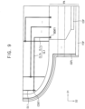
- FIG. 9 is an enlarged view showing a lower left portion of a display apparatus according to embodiments not forming part of the claimed invention
- FIG. 10 is a diagram for describing a connection relation between a data line and a connecting line of the display apparatus of FIG. 9 .
- a display apparatus is substantially the same as the display apparatus of FIGS. 4 and 5 except that the connection contact hole through which the connecting line and the data line are connected to each other is disposed in the display area other than the peripheral area so that the data lines electrically connected to the data spider lines are sequentially arranged. Therefore, redundant descriptions thereof will be omitted.
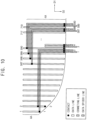
- FIG. 11 is a diagram for describing a connection relation between a data line and a connecting line of a display apparatus according to embodiments.
- FIG. 12 is a sectional view showing a display apparatus according to embodiments
- FIG. 13 is a sectional view showing a display apparatus according to embodiments
- FIG. 14 is a sectional view showing a display apparatus according to embodiments
- FIG. 15 is a sectional view showing a display apparatus according to embodiments.
- FIGS. 12 to 15 illustrate embodiments of display apparatuses in which positions of the connecting line CL, data lines DL_E and DL_O, and the shielding electrode SH are variously changed.
- the data lines may include evennumbered data lines DL_E and odd-numbered data lines DL_O, and some embodiments may correspond to a display apparatus to which a two-data-line (TDL) structure where two data lines correspond to one pixel, a demultiplexer (demux) structure, or the like is applied.
- TDL two-data-line
- demux demultiplexer
- FIG. 16 is a block diagram illustrating an electronic device according to embodiments
- FIG. 17A is a diagram illustrating an example in which the electronic device of FIG. 16 is implemented as a television
- FIG. 17B is a diagram illustrating an example in which the electronic device of FIG. 16 is implemented as a smart phone.
- the electronic device 500 may include a processor 510, a memory device 520, a storage device 530, an input/output (I/O) device 540, a power supply 550, and a display apparatus 560.
- the display apparatus 560 may be the display apparatus of FIG. 1 .
- the electronic device 500 may further include a plurality of ports for communicating with a video card, a sound card, a memory card, a universal serial bus (USB) device, other electronic devices, etc.
- the electronic device 500 may be implemented as a television.
- the electronic device 500 may be implemented as a smart phone.
- the electronic device 500 is not limited thereto.
- the electronic device 500 may be implemented as a cellular phone, a video phone, a smart pad, a smart watch, a tablet PC, a car navigation system, a computer monitor, a laptop, a head mounted display (HMD) apparatus, etc.
- a cellular phone a video phone, a smart pad, a smart watch, a tablet PC, a car navigation system, a computer monitor, a laptop, a head mounted display (HMD) apparatus, etc.
- HMD head mounted display
- the processor 510 may perform various computing functions.
- the processor 510 may be a microprocessor, a central processing unit (CPU), an application processor (AP), etc.
- the processor 510 may be coupled to other components via an address bus, a control bus, a data bus, etc. Further, the processor 510 may be coupled to an extended bus such as a peripheral component interconnection (PCI) bus.
- the memory device 520 may store data for operations of the electronic device 500.
- the memory device 520 may include at least one non-volatile memory device such as an erasable programmable read-only memory (EPROM) device, an electrically erasable programmable read-only memory (EEPROM) device, a flash memory device, a phase change random access memory (PRAM) device, a resistance random access memory (RRAM) device, a nano floating gate memory (NFGM) device, a polymer random access memory (PoRAM) device, a magnetic random access memory (MRAM) device, a ferroelectric random access memory (FRAM) device, etc. and/or at least one volatile memory device such as a dynamic random access memory (DRAM) device, a static random access memory (SRAM) device, a mobile DRAM device, etc.
- EPROM erasable programmable read-only memory
- EEPROM electrically erasable programmable read-only memory
- flash memory device a phase change random access memory (PRAM) device, a resistance random access memory (RRAM) device, a nano floating gate
- the storage device 530 may include a solid state drive (SSD) device, a hard disk drive (HDD) device, a CD-ROM device, etc.
- the I/O device 540 may include an input device such as a keyboard, a keypad, a mouse device, a touch-pad, a touch-screen, etc., and an output device such as a printer, a speaker, etc.
- the power supply 550 may provide power for operations of the electronic device 500.
- the display apparatus 560 may be coupled to other components via the buses or other communication links.
- the I/O device 540 may include the display apparatus 560.
- the display apparatus 560 may have a structure in which a data spider line for a part of an edge of a display area is connected to a data line through a connecting line, so that a width of a bezel, which is a non-display area, at an L-cut part (see FIG. 4 , etc.) of the edge of the display device may be reduced.
- the connecting line may be shielded from other signal wires by the shielding electrode. Since these are described above, duplicated description related thereto will not be repeated.
- the present disclosure may be applied to a display apparatus (e.g., an organic light emitting display device and the like) and an electronic device including the display apparatus.
- a display apparatus e.g., an organic light emitting display device and the like
- the present disclosure may be applied to a smart phone, a cellular phone, a video phone, a smart pad, a smart watch, a tablet PC, a car navigation system, a television, a computer monitor, a laptop, a head mounted display apparatus, etc.
Landscapes
- Engineering & Computer Science (AREA)
- Microelectronics & Electronic Packaging (AREA)
- Physics & Mathematics (AREA)
- Geometry (AREA)
- Optics & Photonics (AREA)
- Devices For Indicating Variable Information By Combining Individual Elements (AREA)
- Electroluminescent Light Sources (AREA)
Applications Claiming Priority (2)
| Application Number | Priority Date | Filing Date | Title |
|---|---|---|---|
| KR1020180083825A KR102528500B1 (ko) | 2018-07-19 | 2018-07-19 | 표시 장치 |
| PCT/KR2019/008669 WO2020017835A1 (ko) | 2018-07-19 | 2019-07-12 | 표시 장치 |
Publications (3)
| Publication Number | Publication Date |
|---|---|
| EP3813137A1 EP3813137A1 (en) | 2021-04-28 |
| EP3813137A4 EP3813137A4 (en) | 2021-08-11 |
| EP3813137B1 true EP3813137B1 (en) | 2025-07-09 |
Family
ID=69164613
Family Applications (1)
| Application Number | Title | Priority Date | Filing Date |
|---|---|---|---|
| EP19837592.5A Active EP3813137B1 (en) | 2018-07-19 | 2019-07-12 | Display device |
Country Status (6)
| Country | Link |
|---|---|
| US (2) | US12035595B2 (https=) |
| EP (1) | EP3813137B1 (https=) |
| JP (1) | JP7553428B2 (https=) |
| KR (2) | KR102528500B1 (https=) |
| CN (2) | CN112840475B (https=) |
| WO (1) | WO2020017835A1 (https=) |
Families Citing this family (39)
| Publication number | Priority date | Publication date | Assignee | Title |
|---|---|---|---|---|
| KR102555841B1 (ko) * | 2018-10-30 | 2023-07-17 | 삼성디스플레이 주식회사 | 표시 장치 |
| KR102798966B1 (ko) | 2019-04-01 | 2025-04-24 | 삼성디스플레이 주식회사 | 전자 장치 |
| KR102772543B1 (ko) * | 2019-06-13 | 2025-02-26 | 삼성디스플레이 주식회사 | 표시 장치 |
| KR102845509B1 (ko) | 2019-08-07 | 2025-08-12 | 삼성디스플레이 주식회사 | 디스플레이 장치 및 그 제조방법 |
| KR102866752B1 (ko) | 2019-09-05 | 2025-09-30 | 삼성디스플레이 주식회사 | 표시 장치 |
| KR102779180B1 (ko) | 2019-09-16 | 2025-03-10 | 삼성디스플레이 주식회사 | 표시 장치 |
| KR102776380B1 (ko) | 2019-09-27 | 2025-03-10 | 삼성디스플레이 주식회사 | 표시장치 |
| KR20210061505A (ko) | 2019-11-19 | 2021-05-28 | 삼성디스플레이 주식회사 | 표시 장치 |
| KR102849776B1 (ko) * | 2020-03-06 | 2025-08-26 | 삼성디스플레이 주식회사 | 표시 장치 |
| KR102733852B1 (ko) * | 2020-04-29 | 2024-11-27 | 삼성디스플레이 주식회사 | 유기발광 디스플레이 장치 및 그 제조방법 |
| WO2021223189A1 (zh) * | 2020-05-07 | 2021-11-11 | 京东方科技集团股份有限公司 | 阵列基板和显示装置 |
| KR102827182B1 (ko) * | 2020-05-29 | 2025-07-02 | 삼성디스플레이 주식회사 | 디스플레이 장치 |
| KR102888565B1 (ko) | 2020-12-01 | 2025-11-21 | 삼성디스플레이 주식회사 | 표시 장치 |
| KR102838156B1 (ko) * | 2020-12-23 | 2025-07-24 | 삼성디스플레이 주식회사 | 표시 장치 |
| GB2610957A (en) | 2021-01-29 | 2023-03-22 | Boe Technology Group Co Ltd | Display substrate and display device |
| KR102835592B1 (ko) | 2021-03-08 | 2025-07-21 | 삼성디스플레이 주식회사 | 표시 장치 |
| KR20220144451A (ko) | 2021-04-19 | 2022-10-27 | 삼성디스플레이 주식회사 | 디스플레이 장치 |
| US12484396B2 (en) * | 2021-04-30 | 2025-11-25 | Chengdu Boe Optoelectronics Technology Co., Ltd. | Array substrate and display device |
| KR102893693B1 (ko) | 2021-07-26 | 2025-12-01 | 삼성디스플레이 주식회사 | 표시장치 |
| KR20230067750A (ko) | 2021-11-08 | 2023-05-17 | 삼성디스플레이 주식회사 | 표시 패널 및 이를 포함하는 전자 장치 |
| CN116203774A (zh) * | 2021-11-30 | 2023-06-02 | 江西兴泰科技股份有限公司 | 一种具有外围裂缝检测电路的柔性电子纸 |
| KR20230114838A (ko) | 2022-01-25 | 2023-08-02 | 삼성디스플레이 주식회사 | 표시 장치 |
| KR20230117018A (ko) | 2022-01-28 | 2023-08-07 | 삼성디스플레이 주식회사 | 표시 장치 |
| US12293700B2 (en) * | 2022-04-20 | 2025-05-06 | Chengdu Boe Optoelectronics Technology Co., Ltd. | Display panel and display apparatus |
| CN115207073B (zh) * | 2022-04-25 | 2023-10-24 | 京东方科技集团股份有限公司 | 显示基板及显示装置 |
| TWI822016B (zh) * | 2022-04-28 | 2023-11-11 | 元太科技工業股份有限公司 | 顯示裝置 |
| US12525161B2 (en) | 2022-04-28 | 2026-01-13 | E Ink Holdings Inc. | Narrow border reflective display device |
| US12610701B2 (en) | 2022-04-28 | 2026-04-21 | Chengdu Boe Optoelectronics Technology Co., Ltd. | Display substrate, manufacturing method therefor, and display device |
| US20230397462A1 (en) * | 2022-06-03 | 2023-12-07 | Samsung Display Co., Ltd. | Display device |
| WO2024000346A1 (zh) * | 2022-06-30 | 2024-01-04 | 京东方科技集团股份有限公司 | 显示基板和显示装置 |
| CN115132760B (zh) * | 2022-06-30 | 2025-10-03 | 武汉华星光电半导体显示技术有限公司 | 显示面板及显示装置 |
| US20240119889A1 (en) * | 2022-10-07 | 2024-04-11 | Samsung Display Co., Ltd. | Display device |
| KR20240092973A (ko) * | 2022-12-15 | 2024-06-24 | 엘지디스플레이 주식회사 | 디스플레이 장치 및 디스플레이 패널 |
| KR20240106246A (ko) | 2022-12-29 | 2024-07-08 | 엘지디스플레이 주식회사 | 픽셀 회로 및 이를 포함하는 표시 장치 |
| KR20240120773A (ko) * | 2023-01-31 | 2024-08-08 | 엘지디스플레이 주식회사 | 디스플레이 패널 및 디스플레이 장치 |
| US20240397766A1 (en) * | 2023-05-26 | 2024-11-28 | Samsung Display Co., Ltd. | Display apparatus |
| KR20250050157A (ko) * | 2023-10-05 | 2025-04-15 | 삼성디스플레이 주식회사 | 표시 장치 |
| KR20250104351A (ko) * | 2023-12-29 | 2025-07-08 | 엘지디스플레이 주식회사 | 표시 장치 |
| KR20250132586A (ko) | 2024-02-28 | 2025-09-05 | 삼성디스플레이 주식회사 | 디스플레이 장치 |
Citations (1)
| Publication number | Priority date | Publication date | Assignee | Title |
|---|---|---|---|---|
| WO2018062023A1 (ja) * | 2016-09-27 | 2018-04-05 | シャープ株式会社 | 表示パネル |
Family Cites Families (16)
| Publication number | Priority date | Publication date | Assignee | Title |
|---|---|---|---|---|
| JP2003288044A (ja) | 2002-03-28 | 2003-10-10 | Tdk Corp | ディスプレイ装置 |
| KR20060001702A (ko) | 2004-06-30 | 2006-01-06 | 엘지.필립스 엘시디 주식회사 | 부식방지를 위한 액정표시소자 및 그 제조방법 |
| KR100603836B1 (ko) | 2004-11-30 | 2006-07-24 | 엘지.필립스 엘시디 주식회사 | 유기전계발광 소자 및 그의 제조방법 |
| KR100721949B1 (ko) * | 2005-09-16 | 2007-05-25 | 삼성에스디아이 주식회사 | 유기 전계발광 표시장치 |
| KR101433109B1 (ko) * | 2007-10-16 | 2014-08-26 | 엘지디스플레이 주식회사 | 액정표시장치용 어레이 기판 및 그 제조방법 |
| KR20100075058A (ko) * | 2008-12-24 | 2010-07-02 | 삼성전자주식회사 | 박막 트랜지스터 기판 및 그 제조 방법 |
| KR101602332B1 (ko) | 2009-12-01 | 2016-03-11 | 엘지디스플레이 주식회사 | 액정표시장치 및 그 제조방법 |
| TWI692280B (zh) | 2013-03-07 | 2020-04-21 | 日商半導體能源研究所股份有限公司 | 顯示裝置 |
| US9430180B2 (en) | 2013-11-15 | 2016-08-30 | Semiconductor Energy Laboratory Co., Ltd | Display panel and electronic device |
| WO2016140281A1 (ja) | 2015-03-02 | 2016-09-09 | シャープ株式会社 | アクティブマトリクス基板、及びそれを備えた表示装置 |
| KR102481377B1 (ko) * | 2015-08-13 | 2022-12-27 | 삼성디스플레이 주식회사 | 어레이 기판 |
| KR102427312B1 (ko) | 2015-11-27 | 2022-08-01 | 엘지디스플레이 주식회사 | 유기발광표시패널 및 유기발광표시장치 |
| KR20180030325A (ko) | 2016-09-13 | 2018-03-22 | 삼성디스플레이 주식회사 | 표시장치 |
| KR102743728B1 (ko) * | 2016-11-08 | 2024-12-19 | 삼성디스플레이 주식회사 | 표시 장치 |
| KR102594020B1 (ko) | 2016-12-07 | 2023-10-27 | 삼성디스플레이 주식회사 | 표시 장치 |
| KR102731256B1 (ko) | 2016-12-30 | 2024-11-19 | 엘지디스플레이 주식회사 | 표시장치와 그의 제조방법 |
-
2018
- 2018-07-19 KR KR1020180083825A patent/KR102528500B1/ko active Active
-
2019
- 2019-07-12 JP JP2021502997A patent/JP7553428B2/ja active Active
- 2019-07-12 WO PCT/KR2019/008669 patent/WO2020017835A1/ko not_active Ceased
- 2019-07-12 CN CN201980048341.7A patent/CN112840475B/zh active Active
- 2019-07-12 EP EP19837592.5A patent/EP3813137B1/en active Active
- 2019-07-12 US US17/261,527 patent/US12035595B2/en active Active
- 2019-07-12 CN CN202510129119.7A patent/CN119907550A/zh active Pending
-
2023
- 2023-04-27 KR KR1020230055638A patent/KR102632740B1/ko active Active
-
2024
- 2024-07-08 US US18/766,517 patent/US12563933B2/en active Active
Patent Citations (1)
| Publication number | Priority date | Publication date | Assignee | Title |
|---|---|---|---|---|
| WO2018062023A1 (ja) * | 2016-09-27 | 2018-04-05 | シャープ株式会社 | 表示パネル |
Also Published As
| Publication number | Publication date |
|---|---|
| US12035595B2 (en) | 2024-07-09 |
| KR20200010697A (ko) | 2020-01-31 |
| US20240365621A1 (en) | 2024-10-31 |
| KR102528500B1 (ko) | 2023-05-04 |
| US20210273035A1 (en) | 2021-09-02 |
| US12563933B2 (en) | 2026-02-24 |
| CN112840475B (zh) | 2025-02-25 |
| KR20230062521A (ko) | 2023-05-09 |
| WO2020017835A1 (ko) | 2020-01-23 |
| CN112840475A (zh) | 2021-05-25 |
| EP3813137A4 (en) | 2021-08-11 |
| CN119907550A (zh) | 2025-04-29 |
| EP3813137A1 (en) | 2021-04-28 |
| JP2021530746A (ja) | 2021-11-11 |
| JP7553428B2 (ja) | 2024-09-18 |
| KR102632740B1 (ko) | 2024-02-05 |
Similar Documents
| Publication | Publication Date | Title |
|---|---|---|
| US12563933B2 (en) | Display apparatus | |
| CN110310961B (zh) | 具有凹口的显示装置 | |
| KR102804879B1 (ko) | 표시 장치 | |
| CN110660812B (zh) | 显示装置 | |
| JP7537880B2 (ja) | 表示装置 | |
| US11665938B2 (en) | Display apparatus | |
| US20230141982A1 (en) | Display apparatus | |
| CN111509003B (zh) | 显示设备 | |
| US10700150B2 (en) | Unit pixel and organic light emitting display device including the same | |
| CN116071996A (zh) | 显示装置 |
Legal Events
| Date | Code | Title | Description |
|---|---|---|---|
| STAA | Information on the status of an ep patent application or granted ep patent |
Free format text: STATUS: THE INTERNATIONAL PUBLICATION HAS BEEN MADE |
|
| PUAI | Public reference made under article 153(3) epc to a published international application that has entered the european phase |
Free format text: ORIGINAL CODE: 0009012 |
|
| STAA | Information on the status of an ep patent application or granted ep patent |
Free format text: STATUS: REQUEST FOR EXAMINATION WAS MADE |
|
| 17P | Request for examination filed |
Effective date: 20210119 |
|
| AK | Designated contracting states |
Kind code of ref document: A1 Designated state(s): AL AT BE BG CH CY CZ DE DK EE ES FI FR GB GR HR HU IE IS IT LI LT LU LV MC MK MT NL NO PL PT RO RS SE SI SK SM TR |
|
| AX | Request for extension of the european patent |
Extension state: BA ME |
|
| REG | Reference to a national code |
Ref country code: DE Ref legal event code: R079 Free format text: PREVIOUS MAIN CLASS: H01L0051520000 Ipc: H01L0027320000 Ref document number: 602019072390 Country of ref document: DE |
|
| A4 | Supplementary search report drawn up and despatched |
Effective date: 20210713 |
|
| RIC1 | Information provided on ipc code assigned before grant |
Ipc: H01L 27/32 20060101AFI20210708BHEP |
|
| DAV | Request for validation of the european patent (deleted) | ||
| DAX | Request for extension of the european patent (deleted) | ||
| P01 | Opt-out of the competence of the unified patent court (upc) registered |
Effective date: 20230516 |
|
| STAA | Information on the status of an ep patent application or granted ep patent |
Free format text: STATUS: EXAMINATION IS IN PROGRESS |
|
| 17Q | First examination report despatched |
Effective date: 20230626 |
|
| REG | Reference to a national code |
Ref country code: DE Ref legal event code: R079 Free format text: PREVIOUS MAIN CLASS: H01L0027320000 Ipc: H10K0059131000 Ref document number: 602019072390 Country of ref document: DE |
|
| GRAP | Despatch of communication of intention to grant a patent |
Free format text: ORIGINAL CODE: EPIDOSNIGR1 |
|
| STAA | Information on the status of an ep patent application or granted ep patent |
Free format text: STATUS: GRANT OF PATENT IS INTENDED |
|
| RIC1 | Information provided on ipc code assigned before grant |
Ipc: H10K 59/131 20230101AFI20250113BHEP |
|
| INTG | Intention to grant announced |
Effective date: 20250129 |
|
| GRAS | Grant fee paid |
Free format text: ORIGINAL CODE: EPIDOSNIGR3 |
|
| GRAA | (expected) grant |
Free format text: ORIGINAL CODE: 0009210 |
|
| STAA | Information on the status of an ep patent application or granted ep patent |
Free format text: STATUS: THE PATENT HAS BEEN GRANTED |
|
| AK | Designated contracting states |
Kind code of ref document: B1 Designated state(s): AL AT BE BG CH CY CZ DE DK EE ES FI FR GB GR HR HU IE IS IT LI LT LU LV MC MK MT NL NO PL PT RO RS SE SI SK SM TR |
|
| REG | Reference to a national code |
Ref country code: GB Ref legal event code: FG4D |
|
| REG | Reference to a national code |
Ref country code: CH Ref legal event code: EP |
|
| REG | Reference to a national code |
Ref country code: IE Ref legal event code: FG4D |
|
| REG | Reference to a national code |
Ref country code: DE Ref legal event code: R096 Ref document number: 602019072390 Country of ref document: DE |
|
| PGFP | Annual fee paid to national office [announced via postgrant information from national office to epo] |
Ref country code: DE Payment date: 20250721 Year of fee payment: 7 |
|
| PGFP | Annual fee paid to national office [announced via postgrant information from national office to epo] |
Ref country code: GB Payment date: 20250722 Year of fee payment: 7 |
|
| PGFP | Annual fee paid to national office [announced via postgrant information from national office to epo] |
Ref country code: FR Payment date: 20250725 Year of fee payment: 7 |
|
| REG | Reference to a national code |
Ref country code: NL Ref legal event code: MP Effective date: 20250709 |
|
| PG25 | Lapsed in a contracting state [announced via postgrant information from national office to epo] |
Ref country code: PT Free format text: LAPSE BECAUSE OF FAILURE TO SUBMIT A TRANSLATION OF THE DESCRIPTION OR TO PAY THE FEE WITHIN THE PRESCRIBED TIME-LIMIT Effective date: 20251110 |
|
| PG25 | Lapsed in a contracting state [announced via postgrant information from national office to epo] |
Ref country code: NL Free format text: LAPSE BECAUSE OF FAILURE TO SUBMIT A TRANSLATION OF THE DESCRIPTION OR TO PAY THE FEE WITHIN THE PRESCRIBED TIME-LIMIT Effective date: 20250709 |
|
| REG | Reference to a national code |
Ref country code: AT Ref legal event code: MK05 Ref document number: 1813126 Country of ref document: AT Kind code of ref document: T Effective date: 20250709 |
|
| PG25 | Lapsed in a contracting state [announced via postgrant information from national office to epo] |
Ref country code: IS Free format text: LAPSE BECAUSE OF FAILURE TO SUBMIT A TRANSLATION OF THE DESCRIPTION OR TO PAY THE FEE WITHIN THE PRESCRIBED TIME-LIMIT Effective date: 20251109 |
|
| PG25 | Lapsed in a contracting state [announced via postgrant information from national office to epo] |
Ref country code: NO Free format text: LAPSE BECAUSE OF FAILURE TO SUBMIT A TRANSLATION OF THE DESCRIPTION OR TO PAY THE FEE WITHIN THE PRESCRIBED TIME-LIMIT Effective date: 20251009 |
|
| REG | Reference to a national code |
Ref country code: LT Ref legal event code: MG9D |
|
| PG25 | Lapsed in a contracting state [announced via postgrant information from national office to epo] |
Ref country code: AT Free format text: LAPSE BECAUSE OF FAILURE TO SUBMIT A TRANSLATION OF THE DESCRIPTION OR TO PAY THE FEE WITHIN THE PRESCRIBED TIME-LIMIT Effective date: 20250709 |
|
| PG25 | Lapsed in a contracting state [announced via postgrant information from national office to epo] |
Ref country code: FI Free format text: LAPSE BECAUSE OF FAILURE TO SUBMIT A TRANSLATION OF THE DESCRIPTION OR TO PAY THE FEE WITHIN THE PRESCRIBED TIME-LIMIT Effective date: 20250709 |
|
| PG25 | Lapsed in a contracting state [announced via postgrant information from national office to epo] |
Ref country code: HR Free format text: LAPSE BECAUSE OF FAILURE TO SUBMIT A TRANSLATION OF THE DESCRIPTION OR TO PAY THE FEE WITHIN THE PRESCRIBED TIME-LIMIT Effective date: 20250709 |
|
| PG25 | Lapsed in a contracting state [announced via postgrant information from national office to epo] |
Ref country code: GR Free format text: LAPSE BECAUSE OF FAILURE TO SUBMIT A TRANSLATION OF THE DESCRIPTION OR TO PAY THE FEE WITHIN THE PRESCRIBED TIME-LIMIT Effective date: 20251010 |
|
| PG25 | Lapsed in a contracting state [announced via postgrant information from national office to epo] |
Ref country code: SE Free format text: LAPSE BECAUSE OF FAILURE TO SUBMIT A TRANSLATION OF THE DESCRIPTION OR TO PAY THE FEE WITHIN THE PRESCRIBED TIME-LIMIT Effective date: 20250709 |
|
| PG25 | Lapsed in a contracting state [announced via postgrant information from national office to epo] |
Ref country code: LV Free format text: LAPSE BECAUSE OF FAILURE TO SUBMIT A TRANSLATION OF THE DESCRIPTION OR TO PAY THE FEE WITHIN THE PRESCRIBED TIME-LIMIT Effective date: 20250709 |
|
| PG25 | Lapsed in a contracting state [announced via postgrant information from national office to epo] |
Ref country code: BG Free format text: LAPSE BECAUSE OF FAILURE TO SUBMIT A TRANSLATION OF THE DESCRIPTION OR TO PAY THE FEE WITHIN THE PRESCRIBED TIME-LIMIT Effective date: 20250709 Ref country code: PL Free format text: LAPSE BECAUSE OF FAILURE TO SUBMIT A TRANSLATION OF THE DESCRIPTION OR TO PAY THE FEE WITHIN THE PRESCRIBED TIME-LIMIT Effective date: 20250709 |
|
| PG25 | Lapsed in a contracting state [announced via postgrant information from national office to epo] |
Ref country code: RS Free format text: LAPSE BECAUSE OF FAILURE TO SUBMIT A TRANSLATION OF THE DESCRIPTION OR TO PAY THE FEE WITHIN THE PRESCRIBED TIME-LIMIT Effective date: 20251009 |
|
| PG25 | Lapsed in a contracting state [announced via postgrant information from national office to epo] |
Ref country code: ES Free format text: LAPSE BECAUSE OF FAILURE TO SUBMIT A TRANSLATION OF THE DESCRIPTION OR TO PAY THE FEE WITHIN THE PRESCRIBED TIME-LIMIT Effective date: 20250709 |
|
| REG | Reference to a national code |
Ref country code: CH Ref legal event code: H13 Free format text: ST27 STATUS EVENT CODE: U-0-0-H10-H13 (AS PROVIDED BY THE NATIONAL OFFICE) Effective date: 20260224 |
|
| PG25 | Lapsed in a contracting state [announced via postgrant information from national office to epo] |
Ref country code: LU Free format text: LAPSE BECAUSE OF NON-PAYMENT OF DUE FEES Effective date: 20250712 Ref country code: RO Free format text: LAPSE BECAUSE OF FAILURE TO SUBMIT A TRANSLATION OF THE DESCRIPTION OR TO PAY THE FEE WITHIN THE PRESCRIBED TIME-LIMIT Effective date: 20250709 |
|
| REG | Reference to a national code |
Ref country code: BE Ref legal event code: MM Effective date: 20250731 |
|
| PG25 | Lapsed in a contracting state [announced via postgrant information from national office to epo] |
Ref country code: SM Free format text: LAPSE BECAUSE OF FAILURE TO SUBMIT A TRANSLATION OF THE DESCRIPTION OR TO PAY THE FEE WITHIN THE PRESCRIBED TIME-LIMIT Effective date: 20250709 |
|
| PG25 | Lapsed in a contracting state [announced via postgrant information from national office to epo] |
Ref country code: DK Free format text: LAPSE BECAUSE OF FAILURE TO SUBMIT A TRANSLATION OF THE DESCRIPTION OR TO PAY THE FEE WITHIN THE PRESCRIBED TIME-LIMIT Effective date: 20250709 |
|
| PG25 | Lapsed in a contracting state [announced via postgrant information from national office to epo] |
Ref country code: BE Free format text: LAPSE BECAUSE OF NON-PAYMENT OF DUE FEES Effective date: 20250731 Ref country code: IT Free format text: LAPSE BECAUSE OF FAILURE TO SUBMIT A TRANSLATION OF THE DESCRIPTION OR TO PAY THE FEE WITHIN THE PRESCRIBED TIME-LIMIT Effective date: 20250709 |
|
| PG25 | Lapsed in a contracting state [announced via postgrant information from national office to epo] |
Ref country code: CH Free format text: LAPSE BECAUSE OF NON-PAYMENT OF DUE FEES Effective date: 20250731 Ref country code: CZ Free format text: LAPSE BECAUSE OF FAILURE TO SUBMIT A TRANSLATION OF THE DESCRIPTION OR TO PAY THE FEE WITHIN THE PRESCRIBED TIME-LIMIT Effective date: 20250709 |
|
| PG25 | Lapsed in a contracting state [announced via postgrant information from national office to epo] |
Ref country code: EE Free format text: LAPSE BECAUSE OF FAILURE TO SUBMIT A TRANSLATION OF THE DESCRIPTION OR TO PAY THE FEE WITHIN THE PRESCRIBED TIME-LIMIT Effective date: 20250709 Ref country code: SK Free format text: LAPSE BECAUSE OF FAILURE TO SUBMIT A TRANSLATION OF THE DESCRIPTION OR TO PAY THE FEE WITHIN THE PRESCRIBED TIME-LIMIT Effective date: 20250709 |