EP3806173A1 - Light-emitting diode package - Google Patents
Light-emitting diode package Download PDFInfo
- Publication number
- EP3806173A1 EP3806173A1 EP19820318.4A EP19820318A EP3806173A1 EP 3806173 A1 EP3806173 A1 EP 3806173A1 EP 19820318 A EP19820318 A EP 19820318A EP 3806173 A1 EP3806173 A1 EP 3806173A1
- Authority
- EP
- European Patent Office
- Prior art keywords
- lead
- electrode pad
- exposing plane
- light emitting
- emitting diode
- Prior art date
- Legal status (The legal status is an assumption and is not a legal conclusion. Google has not performed a legal analysis and makes no representation as to the accuracy of the status listed.)
- Pending
Links
Images






Classifications
-
- H—ELECTRICITY
- H10—SEMICONDUCTOR DEVICES; ELECTRIC SOLID-STATE DEVICES NOT OTHERWISE PROVIDED FOR
- H10H—INORGANIC LIGHT-EMITTING SEMICONDUCTOR DEVICES HAVING POTENTIAL BARRIERS
- H10H20/00—Individual inorganic light-emitting semiconductor devices having potential barriers, e.g. light-emitting diodes [LED]
- H10H20/80—Constructional details
- H10H20/85—Packages
- H10H20/857—Interconnections, e.g. lead-frames, bond wires or solder balls
-
- H—ELECTRICITY
- H10—SEMICONDUCTOR DEVICES; ELECTRIC SOLID-STATE DEVICES NOT OTHERWISE PROVIDED FOR
- H10H—INORGANIC LIGHT-EMITTING SEMICONDUCTOR DEVICES HAVING POTENTIAL BARRIERS
- H10H20/00—Individual inorganic light-emitting semiconductor devices having potential barriers, e.g. light-emitting diodes [LED]
- H10H20/80—Constructional details
- H10H20/81—Bodies
- H10H20/819—Bodies characterised by their shape, e.g. curved or truncated substrates
-
- H—ELECTRICITY
- H10—SEMICONDUCTOR DEVICES; ELECTRIC SOLID-STATE DEVICES NOT OTHERWISE PROVIDED FOR
- H10H—INORGANIC LIGHT-EMITTING SEMICONDUCTOR DEVICES HAVING POTENTIAL BARRIERS
- H10H20/00—Individual inorganic light-emitting semiconductor devices having potential barriers, e.g. light-emitting diodes [LED]
- H10H20/80—Constructional details
- H10H20/83—Electrodes
- H10H20/831—Electrodes characterised by their shape
-
- H—ELECTRICITY
- H10—SEMICONDUCTOR DEVICES; ELECTRIC SOLID-STATE DEVICES NOT OTHERWISE PROVIDED FOR
- H10H—INORGANIC LIGHT-EMITTING SEMICONDUCTOR DEVICES HAVING POTENTIAL BARRIERS
- H10H20/00—Individual inorganic light-emitting semiconductor devices having potential barriers, e.g. light-emitting diodes [LED]
- H10H20/80—Constructional details
- H10H20/85—Packages
-
- H—ELECTRICITY
- H10—SEMICONDUCTOR DEVICES; ELECTRIC SOLID-STATE DEVICES NOT OTHERWISE PROVIDED FOR
- H10H—INORGANIC LIGHT-EMITTING SEMICONDUCTOR DEVICES HAVING POTENTIAL BARRIERS
- H10H20/00—Individual inorganic light-emitting semiconductor devices having potential barriers, e.g. light-emitting diodes [LED]
- H10H20/80—Constructional details
- H10H20/85—Packages
- H10H20/8506—Containers
-
- H—ELECTRICITY
- H10—SEMICONDUCTOR DEVICES; ELECTRIC SOLID-STATE DEVICES NOT OTHERWISE PROVIDED FOR
- H10W—GENERIC PACKAGES, INTERCONNECTIONS, CONNECTORS OR OTHER CONSTRUCTIONAL DETAILS OF DEVICES COVERED BY CLASS H10
- H10W90/00—Package configurations
Definitions
- Embodiments of the present disclosure relate to a light emitting diode package, and more particularly, to a light emitting diode package capable of improving luminous efficacy of light emitted therefrom.
- a light emitting diode is an inorganic light source adapted to generate light through recombination of electrons and holes.
- light emitting diodes are used in various fields including a display apparatus, a vehicular lamp, general lighting, and the like.
- the light emitting diode has various advantages, such as longer lifespan, lower power consumption and rapider response time than existing light sources. With such advantages, light emitting diodes have replaced existing light sources.
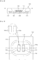
- FIG. 1 is a top plan view of a typical light emitting diode package and FIG. 2 is a cross-sectional view taken along line S-S' of FIG. 1 .
- a typical light emitting diode package includes a first lead and a second lead separated from each other and a housing adapted to support the first lead and the second lead.
- the housing may have a cavity 15 formed to expose upper surfaces of the first lead and the second lead.
- the cavity 15 is formed to open a top portion of a central region of the housing while exposing the first lead and the second lead through a lower portion thereof.
- a light emitting diode chip is mounted on the first lead. The light emitting diode chip is electrically connected to the first lead and the second lead through a wire.
- the first lead and the second lead are exposed over a bottom surface of the cavity 15.
- the housing is formed of a white synthetic resin
- the first lead and the second lead have lower reflectivity than the housing, thereby causing deterioration in luminous efficacy of the light emitting diode package.
- the light emitting diode chip is electrically connected to the first lead and the second lead through the wire, there can be a problem of obstruction of light emitted from the light emitting diode chip due to the wire.
- Embodiments of the present disclosure provide a light emitting diode package capable of improving luminous efficacy.
- a light emitting diode package includes: a light emitting diode chip provided at a lower side thereof with a first electrode pad and a second electrode pad; a first lead and a second lead spaced apart from each other and contacting the first electrode pad and the second electrode pad of the light emitting diode chip to be electrically connected thereto, respectively; and a housing formed to surround the first lead and the second lead and having a cavity open at a top portion thereof.
- the first lead and the second lead have a first lead exposing plane and a second lead exposing plane disposed on a bottom surface of the cavity of the housing and partially exposing the first lead and the second lead, respectively.
- the first lead exposing plane and the second lead exposing plane may be formed in sizes and shapes corresponding to the first electrode pad and the second electrode pad, respectively.
- Each of the first lead and the second lead may be formed on an upper surface thereof with a groove such that only the first lead exposing plane and the second lead exposing plane are exposed to the bottom surface of the cavity therethrough.
- the grooves of the first lead and the second lead may be occupied with the housing.
- the sizes and shapes of the first lead exposing plane and the second lead exposing plane may be the same as those of the first electrode pad and the second electrode pad, respectively.
- Each of the first electrode pad and the second electrode pad may have a rectangular shape; each of the first lead exposing plane and the second lead exposing plane may have a rectangular shape; and one side of the rectangular shape of each of the first lead exposing plane and the second lead exposing plane may be placed outside one side of the rectangular shape of each of the first electrode pad and the second electrode pad.
- the first electrode pad and the second electrode pad may contact the first lead exposing plane and the second lead exposing plane, respectively, such that at least one of other sides of the rectangular shape of each of the first lead exposing plane and the second lead exposing plane is coincident with at least one side of each of the first electrode pad and the second electrode pad.
- Each of the first lead exposing plane and the second lead exposing plane may be partially extended in an outward direction.
- Each of the first lead exposing plane and the second lead exposing plane may have a polygonal concave shape.
- Each of the first lead exposing plane and the second lead exposing plane may have an octagonal or dodecagonal concave shape.
- Each of the first lead exposing plane and the second lead exposing plane may have a polygonal shape formed by extending a portion of one side of a rectangular shape in the outward direction.
- Each of the first lead exposing plane and the second lead exposing plane may have a polygonal shape formed by extending a portion of each of three sides of a rectangular shape in the outward direction.
- Each of the first lead exposing plane and the second lead exposing plane may have a hexagonal shape; the first electrode pad and the second electrode pad may contact the first lead exposing plane and the second lead exposing plane, respectively, such that at least one side of each of the first and second electrode pads is coincident with at least one side of each of the first and second lead exposing planes, while allowing the entirety of the first electrode pad and the second electrode pad to contact the first lead exposing plane and the second lead exposing plane, respectively.
- Each of the first lead exposing plane and the second lead exposing plane may have a surface not contacting the first electrode pad or the second electrode pad at a location opposite to at least one side thereof at which the first electrode pad and the second electrode pad are coincident with the first lead exposing plane and the second lead exposing plane, respectively.
- Each of the first lead exposing plane and the second lead exposing plane may have a surface not contacting the first electrode pad or the second electrode pad at opposite locations with respect to at least one side thereof at which the first electrode pad and the second electrode pad are coincident with the first lead exposing plane and the second lead exposing plane, respectively.
- At least one corner of each of the first electrode pad and the second electrode pad may contact at least one side of each of the first lead exposing plane and the second lead exposing plane each having the hexagonal shape.
- Each of the first lead and the second lead may be partially exposed to the bottom surface of the cavity of the housing and may include a Zener diode mounting portion and a Zener diode connecting portion to which a Zener diode chip is electrically connected.
- Each of a first groove formed on the first lead and a second groove formed on the second lead may have an asymmetrical structure in which one side thereof is asymmetrical to the other side thereof opposite to the one side.
- each of the first groove and the second groove may be placed under an inner surface of the housing defining the cavity. Further, a portion of the other side surface of each of the first groove and the second groove may be placed between the inner surface of the housing and an outer surface of the housing.
- a width from one side of the first groove to one side of the first lead exposing plane facing the one side of the first groove may be greater than a width from the other side of the first lead exposing plane to one side of the Zener diode mounting portion facing the other side of the first lead exposing plane.
- a width from one side of the second groove to one side of the second lead exposing plane facing the one side of the second groove may be greater than a width from the other side of the second lead exposing plane to one side of the Zener diode connecting portion facing the other side of the second lead exposing plane.
- a portion of a side surface of each of the first lead and the second lead may be exposed to a side surface of the housing.
- the light emitting diode package may further include a sealing member filling the cavity of the housing.
- a light emitting diode package employs a flip-chip type light emitting diode chip and minimizes exposure of a first lead and a second lead, thereby maximizing luminous efficacy of the light emitting diode package.
- each of the first lead and the second lead for electrical connection to the light emitting diode chip is formed with a groove on an upper surface thereof, thereby minimizing exposure of the first lead and the second lead through a cavity of the housing.
- the first lead and the second lead are formed in greater sizes than a first electrode pad and a second electrode pad formed on the light emitting diode chip, thereby improving bonding strength between the light emitting diode chip and each of the first lead and the second lead while minimizing generation of solder balls protruding from the first lead and the second lead.
- each of the first lead and the second lead exposed to the bottom surface of the cavity for electrical connection to the light emitting diode chip is partially extended in the lateral direction.
- the first electrode pad and the second electrode pad of the light emitting diode chip are placed corresponding to the shapes of the exposed first and second leads, whereby the light emitting diode chip can be placed at an accurate location while minimizing generation of solder balls protruding from the first lead and the second lead.
- FIG. 3 is a perspective view of a light emitting diode package according to a first embodiment of the present disclosure.
- FIG. 4 to FIG. 6 are a top plan view and cross-sectional views of the light emitting diode package according to the first embodiment of the present disclosure, respectively.
- FIG. 5 is a cross-sectional view taken along line A-A' of FIG. 4
- FIG. 6 is a cross-sectional view taken along line B-B' of FIG. 4 .
- a light emitting diode package 100 includes a housing 110, a first lead 120, a second lead 130, and a light emitting diode chip 150.
- the housing 110 is formed to surround the first lead 120 and the second lead 130 so as to support the first lead 120 and the second lead 130. A space between the first lead 120 and the second lead 130 may be occupied by the housing 110.
- the housing 110 may be formed to expose a portion of an upper surface of each of the first lead 120 and the second lead 130 through a cavity 115, instead of completely surrounding the entirety of the first lead 120 and the second lead 130.
- the first lead 120 and the second lead 130 are spaced apart from each other and serve to supply electric power to the light emitting diode chip 150.
- the first lead 120 and the second lead 130 include a first lead exposing plane 120a and a second lead exposing plane 130a, on which the cavity 115 of the housing 110 is partially exposed, respectively.
- the first lead 120 and the second lead 130 may be exposed to a lower surface of the housing 110.
- the first lead 120 and the second lead 130 are formed on upper surfaces thereof with a first groove H1 and a second groove H2, respectively.
- a portion of the first lead 120 corresponding to a location of the light emitting diode chip 150 mounted on the first lead 120 protrudes upwards to form a first lead exposing plane 120a exposed to an inner surface of the cavity 115.
- another portion of the first lead 120 opposite to the portion of the first lead 120 protruding to form the first lead exposing plane 120a may also protrude upwards.
- the first lead 120 is formed with the first groove H1, which has the same shape as the cavity 115 defined in the housing 110, between the protruding portions of the first lead 120 at opposite sides on the upper surface of the first lead 120.
- the entirety of a lower surface of the first lead 120 is exposed to the lower surface of the housing 110.
- the first lead 120 may be restrictively exposed to the cavity 115 of the housing 110.
- the first lead 120 exposed to the cavity 115 may have an exposed size corresponding to the size of a first electrode pad 152 of the light emitting diode chip 150.
- the second lead 130 may have a symmetrical shape to the first lead 120 in sectional view, in which the second groove H2 having a shape corresponding to the cavity 115 defined in the housing 110 is formed on the upper surface of the second lead 130. Further, the entirety of a lower surface of the second lead 130 is exposed to the lower surface of the housing 110.
- a portion of the second lead 130 corresponding to a location of the light emitting diode chip 150 mounted on the second lead 130 protrudes upwards to form a second lead exposing plane 130a exposed to the inner surface of the cavity 115.
- another portion of the second lead 130 opposite to the portion of the second lead 130 protruding to form the second lead exposing plane 130a may also protrude upwards.
- the second lead 130 is formed with the second groove H2 between the protruding portions of the second lead 130 at opposite sides on the upper surface of the second lead 130.
- the second lead 130 may be restrictively exposed to the cavity 115 of the housing 110.
- the second lead 130 exposed to the cavity 115 may have an exposed size corresponding to the size of a second electrode pad 154 of the light emitting diode chip 150.
- the light emitting diode package may include at least one light emitting diode chip 150, which may be placed on the first lead 120 and the second lead 130 exposed to a bottom surface of the cavity 115.
- the light emitting diode chip 150 may be provided at a lower side thereof with the first electrode pad 152 and the second electrode pad 154, and may emit light when electric power is applied thereto through the first electrode pad 152 and the second electrode pad 154.
- the light emitting diode chip 150 includes an n-type semiconductor layer, an active layer, and a p-type semiconductor layer.
- Each of the n-type semiconductor layer, the active layer, and the p-type semiconductor layer may include a III-V group-based compound semiconductor, for example, a nitride semiconductor, such as (Al, Ga, In)N.
- the active layer may be formed on the n-type semiconductor layer and the p-type semiconductor layer may be formed on the active layer.
- the locations of the n-type semiconductor layer and the p-type semiconductor layer may be changed, as needed.
- the n-type semiconductor layer may include n-type dopants (for example, Si) and the p-type semiconductor layer may include p-type dopants (for example, Mg).
- the active layer is interposed between the n-type semiconductor layer and the p-type semiconductor layer, and may include a multi-quantum well (MQW) structure. The composition of the active layer may be adjusted to generate light having a desired peak wavelength.
- MQW multi-quantum well
- the first electrode pad 152 and the second electrode pad 154 on the light emitting diode chip 150 may be electrically connected to the p-type semiconductor layer and the n-type semiconductor layer, respectively, or vice versa.
- the first lead 120 and the second lead 130 exposed to the cavity 115 of the housing 110 have the exposed sizes corresponding to the first electrode pad 152 and the second electrode pad 154 of the light emitting diode chip 150, respectively.
- the light emitting diode chip 150 is mounted on the first lead 120 and the second lead 130 via solders. Accordingly, the first electrode pad 152 and the second electrode pad 154 have sizes corresponding to the first lead 120 and the second lead 130, thereby allowing the light emitting diode chip 150 to be mounted at accurate locations on the first lead 120 and the second lead 130 when the light emitting diode chip 150 is mounted thereon.
- an exposed region of each of the first lead 120 and the second lead 130 may be minimized and an inner surface of the cavity 115 is defined by the housing 110, which has higher reflectivity than a metal forming the first lead 120 and the second lead 130, thereby maximizing luminous efficacy of the light emitting diode package 100.
- a separate wire is not used to supply electric power to the light emitting diode chip 150, light emitted from the light emitting diode chip 150 can be prevented from being obstructed by the wire.
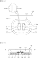
- FIG. 7 and FIG. 8 are a top plan view and a cross-sectional view of a light emitting diode package according to a second embodiment of the present disclosure, respectively.
- FIG. 8 is a cross-sectional view taken along line C-C' of FIG. 7 .
- a light emitting diode package 100 includes a housing 110, a first lead 120, a second lead 130, and a light emitting diode chip 150. Description of the same components as those of the first embodiment will be omitted.
- the light emitting diode package according to this embodiment has the same configuration as the light emitting diode package according to the first embodiment except for the shapes of the first lead exposing plane 120a and the second lead exposing plane 130a, on which the first lead 120 and the second lead 130 are exposed to the cavity 115 of the housing 110.
- the first lead 120 and the second lead 130 are partially exposed at opposite sides of the light emitting diode chip mounting region 150a, on which the light emitting diode chip 150 is mounted. That is, although each of the first lead exposing plane 120a and the second lead exposing plane 130a may have a rectangular shape as in the first embodiment, the first lead exposing plane 120a and the second lead exposing plane 130a may have greater sizes than those of the first embodiment.
- the first lead exposing plane 120a and the second lead exposing plane 130a may have greater sizes than the first electrode pad 152 and the second electrode pad 154 of the light emitting diode chip 150, respectively.
- the first lead exposing plane 120a may have a rectangular shape having an enlarged size in a leftward direction, as compared with the first electrode pad 152, with reference to FIG. 7 and FIG. 8 . That is, when the first electrode pad 152 is brought into contact with the first lead exposing plane 120a, three sides of the rectangular shape of the first electrode pad 152 are coincident with the corresponding three sides of the first lead exposing plane 120a in plan view.
- the second lead exposing plane 130a may have a rectangular shape having an enlarged size in a rightward direction, as compared with the second electrode pad 154, with reference to FIG. 7 and FIG. 8 . That is, when the second electrode pad 154 is brought into contact with the second lead exposing plane 130a, three sides of the rectangular shape of the second electrode pad 154 are coincident with the corresponding three sides of the second lead exposing plane 130a in plan view.
- the first lead exposing plane 120a and the second lead exposing plane 130a may be exposed at the opposite sides of the light emitting diode chip 150.
- the light emitting diode package can prevent generation of solder balls formed by solders sticking out of lateral sides of the first electrode pad 152 and the second electrode pad 154 even when the amount of the solders for bonding the first lead exposing plane 120a and the second lead exposing plane 130a to the first electrode pad 152 and the second electrode pad 154 is increased.
- the solder balls excessively protruding from the lateral sides of the first electrode pad 152 and the second electrode pad 154 can cause short circuit.
- the light emitting diode package 100 according to this embodiment can minimize generation of the solder balls, thereby minimizing failure of the light emitting diode package 100.
- FIG. 9 and FIG. 10 are a top plan view and a cross-sectional view of a light emitting diode package according to a third embodiment of the present disclosure, respectively.
- FIG. 10 is a cross-sectional view taken along line D-D' of FIG. 9 .
- a light emitting diode package 100 includes a housing 110, a first lead 120, a second lead 130, and a light emitting diode chip 150. Description of the same components as those of the first embodiment will be omitted.
- the light emitting diode package according to this embodiment has the same configuration as the light emitting diode package according to the first embodiment except for the shapes of the first lead exposing plane 120a and the second lead exposing plane 130a, on which the first lead 120 and the second lead 130 are exposed to the cavity 115 of the housing 110.
- each of the first lead exposing plane 120a and the second lead exposing plane 130a may have a rectangular shape having one side partially protruding outwards.
- the first lead exposing plane 120a and the second lead exposing plane 130a may have the same shapes as those of the first embodiment except for the outwardly protruding portions thereof.
- first lead exposing plane 120a and the second lead exposing plane 130a may have larger sizes than the first electrode pad 152 and the second electrode pad 154 of the light emitting diode chip 150, in which the size of each of the first and second lead exposing planes 120a, 130a is enlarged by the outwardly protruding portion thereof, as described above.
- the first lead exposing plane 120a may have a ' ' shape formed by extending a portion of the left side of the rectangular shape with reference to FIG. 9 .
- four corners of the first electrode pad 152 having a rectangular shape may be disposed to be coincident with corresponding four corners of the first lead exposing plane 120a.
- the second lead exposing plane 130a may have a ' ' shape formed by extending a portion of the right side of the rectangular shape with reference to FIG. 9 .
- four corners of the second electrode pad 154 having a rectangular shape may be disposed to be coincident with corresponding four corners of the second lead exposing plane 130a.
- the shapes of the first lead exposing plane 120a and the second lead exposing plane 130a correspond to the shapes of the first electrode pad 152 and the second electrode pad 154 and have the lateral sides partially extended in the lateral direction, respectively, whereby the light emitting diode chip 150 can be mounted at accurate locations on the first lead exposing plane 120a and the second lead exposing plane 130a. That is, the light emitting diode chip 150 may be mounted thereon such that the four corners of each of the first electrode pad 152 and the second electrode pad 154 correspond to the four corners of each of the first lead exposing plane 120a and the second lead exposing plane 130a, thereby minimizing a tilting phenomenon upon mounting of the light emitting diode chip 150.
- each of the first lead exposing plane 120a and the second lead exposing plane 130a is partially extended outwards in the lateral direction, thereby minimizing generation of solder balls at the lateral side of the first electrode pad 152 or the second electrode pad 154 even when the amount of solders for bonding the light emitting diode chip 150 is increased.
- FIG. 11 to FIG. 13 are a top plan view and cross-sectional views of a light emitting diode package according to a fourth embodiment of the present disclosure, respectively.
- FIG. 12 is a cross-sectional view taken along line E-E' of FIG. 11
- FIG. 13 is a cross-sectional view taken along line F-F' of FIG. 11 .
- a light emitting diode package 100 includes a housing 110, a first lead 120, a second lead 130, and a light emitting diode chip 150. Description of the same components as those of the first embodiment will be omitted.
- the light emitting diode package according to this embodiment has the same configuration as the light emitting diode package according to the first embodiment except for the shapes of the first lead exposing plane 120a and the second lead exposing plane 130a, on which the first lead 120 and the second lead 130 are exposed to the cavity 115 of the housing 110.
- each of the first lead exposing plane 120a and the second lead exposing plane 130a may have a rectangular shape having three sides partially protruding outwards.
- the first lead exposing plane 120a and the second lead exposing plane 130a may have the same shapes as those of the first embodiment except for the outwardly protruding portions thereof.
- first lead exposing plane 120a and the second lead exposing plane 130a may have larger sizes than the first electrode pad 152 and the second electrode pad 154 of the light emitting diode chip 150, in which the size of each of the first and second lead exposing planes 120a, 130a is enlarged by the outwardly protruding portion thereof, as described above.
- the first lead exposing plane 120a may have a shape formed by extending a portion of the left side of the rectangular shape and a portion of each of the upper and lower sides of the rectangular shape with reference to FIG. 11 . That is, the first lead exposing plane 120a may have a shape formed by outwardly extending a portion of each of the other sides of the rectangular shape excluding the right side thereof. As three sides of the first lead exposing plane 120a are partially extended in the outward direction, four corners of the first electrode pad 152 having a rectangular shape may be disposed to be coincident with corresponding four corners of the first lead exposing plane 120a.
- the second lead exposing plane 130a may have a shape formed by extending a portion of the right side and a portion of each of the upper and lower sides of the rectangular shape with reference to FIG. 11 . That is, the second lead exposing plane 130a may have a shape formed by outwardly extending a portion of each of the other sides of the rectangular shape excluding the left side thereof. As three sides of the second lead exposing plane 130a are partially extended in the outward direction, four corners of the second electrode pad 154 having a rectangular shape may be disposed to be coincident with corresponding four corners of the second lead exposing plane 130a.
- the shapes of the first lead exposing plane 120a and the second lead exposing plane 130a correspond to the shapes of the first electrode pad 152 and the second electrode pad 154 and have the lateral sides partially extended in the outward direction, whereby the light emitting diode chip 150 can be mounted at accurate locations on the first lead exposing plane 120a and the second lead exposing plane 130a. That is, the light emitting diode chip 150 may be mounted thereon such that the four corners of each of the first electrode pad 152 and the second electrode pad 154 correspond to the four corners of each of the first lead exposing plane 120a and the second lead exposing plane 130a, thereby minimizing a tilting phenomenon upon mounting of the light emitting diode chip 150.
- each of the first lead exposing plane 120a and the second lead exposing plane 130a is partially extended in the outward direction, thereby minimizing generation of solder balls at the lateral side of the first electrode pad 152 or the second electrode pad 154 even when the amount of solders for bonding the light emitting diode chip 150 is increased.
- FIG. 14 and FIG. 15 are a top plan view and a cross-sectional view of a light emitting diode package according to a fifth embodiment of the present disclosure, respectively.
- FIG. 15 is a cross-sectional view taken along line G-G' of FIG. 14 .
- a light emitting diode package 100 includes a housing 110, a first lead 120, a second lead 130, and a light emitting diode chip 150. Description of the same components as those of the first embodiment will be omitted.
- the light emitting diode package according to this embodiment has the same configuration as the light emitting diode package according to the first embodiment except for the shapes of the first lead exposing plane 120a and the second lead exposing plane 130a, on which the first lead 120 and the second lead 130 are exposed to the cavity 115 of the housing 110.
- each of the first lead exposing plane 120a and the second lead exposing plane 130a may have a rectangular shape having one side partially protruding outwards.
- the first lead exposing plane 120a and the second lead exposing plane 130a may have the same shapes as those of the first embodiment except for the outwardly protruding portions thereof.
- first lead exposing plane 120a and the second lead exposing plane 130a may have larger sizes than the first electrode pad 152 and the second electrode pad 154 of the light emitting diode chip 150, in which the size of each of the first and second lead exposing planes 120a, 130a is enlarged by the outwardly protruding portion thereof, as described above.
- the first lead exposing plane 120a may have a pentagonal shape having a left side enlarged in the outward direction with reference to FIG. 14 .
- four corners of the first electrode pad 152 having a rectangular shape may be disposed to be coincident with corresponding four corners of the first lead exposing plane 120a.
- the second lead exposing plane 130a may have a pentagonal shape having a right side enlarged in the outward direction with reference to FIG. 14 .
- four corners of the second electrode pad 154 having a rectangular shape may be disposed to be coincident with corresponding four corners of the second lead exposing plane 130a.
- the shapes of the first lead exposing plane 120a and the second lead exposing plane 130a correspond to the shapes of the first electrode pad 152 and the second electrode pad 154 and have the lateral sides partially extended in the lateral direction, respectively, whereby the light emitting diode chip 150 can be mounted at accurate locations on the first lead exposing plane 120a and the second lead exposing plane 130a. That is, the light emitting diode chip 150 may be mounted thereon such that the four corners of each of the first electrode pad 152 and the second electrode pad 154 correspond to the four corners of each of the first lead exposing plane 120a and the second lead exposing plane 130a, thereby minimizing a tilting phenomenon upon mounting the light emitting diode chip 150.
- each of the first lead exposing plane 120a and the second lead exposing plane 130a is partially extended in the lateral direction, thereby minimizing generation of solder balls at the lateral side of the first electrode pad 152 or the second electrode pad 154 even when the amount of solders for bonding the light emitting diode chip 150 is increased.
- FIG. 16 and FIG. 17 are a top plan view and a cross-sectional view of a light emitting diode package according to a sixth embodiment of the present disclosure, respectively.
- FIG. 17 is a cross-sectional view taken along line H-H' of FIG. 16 .
- the light emitting diode package 100 includes a housing 110, a first lead 120, a second lead 130, and a light emitting diode chip 150. Description of the same components as those of the first embodiment will be omitted.
- the light emitting diode package according to this embodiment has the same configuration as the light emitting diode package according to the first embodiment except for the shapes of the first lead exposing plane 120a and the second lead exposing plane 130a, on which the first lead 120 and the second lead 130 are exposed to the cavity 115 of the housing 110.
- each of the first lead exposing plane 120a and the second lead exposing plane 130a may have a rectangular shape having three sides partially protruding outwards.
- the first lead exposing plane 120a and the second lead exposing plane 130a may have the same shapes as those of the first embodiment except for the outwardly protruding portions thereof.
- the shape of each of the first lead exposing plane 120a and the second lead exposing plane 130a is the same as the shape thereof according to the first embodiment except for the outwardly protruding portion.
- first lead exposing plane 120a and the second lead exposing plane 130a may have larger sizes than the first electrode pad 152 and the second electrode pad 154 of the light emitting diode chip 150, in which the size of each of the first and second lead exposing planes 120a, 130a is enlarged by the outwardly protruding portion thereof, as described above.
- the first lead exposing plane 120a may have a shape formed by enlarging the left side and each of the upper and lower sides of the rectangular shape with reference to FIG. 16 . That is, the first lead exposing plane 120a may have a pentagonal shape formed by outwardly enlarging the other sides of the rectangular shape excluding the right side thereof. As three sides of the first lead exposing plane 120a are enlarged in the outward direction, left two corners of the first electrode pad 152 having four corners may be disposed at locations corresponding to middle points of the lateral sides of the pentagonal shape of the first lead exposing plane 120a.
- the second lead exposing plane 130a may have a shape formed by enlarging the right side and each of the upper and lower sides of the rectangular shape with reference to FIG. 16 . That is, the second lead exposing plane 130a may have a pentagonal shape formed by outwardly enlarging the other sides of the rectangular shape excluding the left side thereof. As the three sides of the second lead exposing plane 130a are enlarged in the outward direction, right two corners of the second electrode pad 154 having four corners may be disposed at locations corresponding to middle points of the lateral sides of the pentagonal shape of the second lead exposing plane 130a.
- the shapes of the first lead exposing plane 120a and the second lead exposing plane 130a correspond to the shapes of the first electrode pad 152 and the second electrode pad 154 and have the lateral sides enlarged in the outward direction, respectively, whereby the light emitting diode chip 150 can be mounted at accurate locations on the first lead exposing plane 120a and the second lead exposing plane 130a. Accordingly, the light emitting diode package according to this embodiment can minimize a tilting phenomenon upon mounting the light emitting diode chip 150.
- each of the first lead exposing plane 120a and the second lead exposing plane 130a has the lateral side partially extended in the outward direction, thereby minimizing generation of solder balls at the lateral side of the first electrode pad 152 or the second electrode pad 154 even when the amount of solders for bonding the light emitting diode chip 150 is increased.
- FIG. 18 to FIG. 20 are a top plan view and cross-sectional views of a light emitting diode package according to a seventh embodiment of the present disclosure, respectively.
- FIG. 19 is a cross-sectional view taken along line I-I' of FIG. 18
- FIG. 20 is a cross-sectional view taken along line J-J' of FIG. 18 .
- a light emitting diode package 100 includes a housing 110, a first lead 120, a second lead 130, and a light emitting diode chip 150. Description of the same components as those of the third embodiment will be omitted.
- this embodiment is a modification of the third embodiment and the other embodiments may also be modified as in this embodiment.
- the light emitting diode package 100 may further include a Zener diode mounting portion 122 and a Zener diode connecting portion 132 inside the cavity 115 of the housing 110.
- the locations of the first lead exposing plane 120a and the second lead exposing plane 130a may be adjusted.
- the Zener diode mounting portion 122 and the Zener diode connecting portion 132 may be biased to one side of the cavity 115, as shown in FIG. 18 .
- a Zener diode chip may be mounted on the Zener diode mounting portion 122 and may be electrically connected to the Zener diode connecting portion 132 via a wire.
- the Zener diode chip mounted on the Zener diode mounting portion may be covered by a reflective member.
- the reflective member may be formed of a silicone resin containing a reflective material, such as TiO 2 .
- FIG. 21 to FIG. 23 are views of a light emitting diode package according to an eighth embodiment of the present disclosure, respectively.
- FIG. 21 is a perspective view of a light emitting diode package 200 according to the eighth embodiment.
- FIG. 22 is a top plan view of the light emitting diode package 200 according to the eighth embodiment, showing a first lead 220 and a second lead 230.
- the housing 110 is illustrated with a dotted line.
- FIG. 23 is a cross-sectional view taken along line K1-K2 of FIG. 21 .
- the light emitting diode package 200 according to the eighth embodiment includes a housing 110, a first lead 220, a second lead 230, a light emitting diode chip 150, a Zener diode chip 160, and a molding portion 270.
- the first lead 220 and the second lead 230 have different structures from those of the light emitting diode packages according to the above embodiments. The following description will focus on the structures of the first lead 220 and the second lead 230.
- each of the first groove H1 of the first lead 220 and the second groove H2 of the second lead 230 has an asymmetrical structure in which one side is asymmetrical to the other side.
- one side of each of the first groove H1 and the second groove H2 refers to a side at which the Zener diode mounting portion 222 and the Zener diode connecting portion 232 are placed.
- the other side of each of the first groove H1 and the second groove H2 refers to a side opposite to the one side.
- One side surface of the first groove H1 is placed under an inner surface of the housing 110.
- the one side surface of the first groove H1 refers to a side surface thereof placed at one side of an inner surface of the first lead 220, which defines the first groove H1.
- the inner surface of the housing 110 defines the cavity 115.
- a portion of the other side surface of the first groove H1 facing the one side surface thereof is placed under the cavity 115. This portion corresponds to a side surface of the Zener diode mounting portion 222 in the first lead 220. Further, another portion of the other side surface of the first groove H1 is placed between the inner surface of the housing 110 and an outer surface of the housing 110. A side surface of the first groove H1 corresponding to a portion of the first groove H1 more deeply depressed than other portions of the first groove H1 is connected to a side surface of the Zener diode mounting portion 222.
- the first groove H1 has an asymmetrical structure in which a portion of the other side surface thereof has a greater length than one side surface thereof with reference to the center of the cavity 115.
- the structure wherein the other side surface of the first groove H1 is more deeply depressed than the other portions thereof allows the Zener diode mounting portion 222 to be formed in a sufficiently large area.
- the light emitting diode package 200 according to this embodiment can prevent absorption of light by the first lead 220 and discoloration of the first lead 220 by minimizing the exposed area of the first lead 220 exposed to the cavity 115 of the housing 110, thereby improving reliability.
- the second groove H2 of the second lead 230 may be symmetrical to the first groove H1 of the first lead 220. Accordingly, the second groove H2 of the second lead 230 also has an asymmetrical structure in which a portion of the other side surface thereof has a greater length than one side surface thereof with reference to the center of the cavity 115.
- a width from one side of the first groove H1 to one side of the first lead exposing plane 221 may be greater than a width from the other side of the first lead exposing plane 221 to one side of the Zener diode mounting portion 222.
- the one side of the first groove H1 faces the one side of the first lead exposing plane 221 and the other side of the first lead exposing plane 221 faces the one side of the Zener diode mounting portion 222.
- a width from one side of the second groove H2 to one side of the second lead exposing plane 231 may be greater than a width form the other side of the second lead exposing plane 231 to one side of the Zener diode connecting portion 232.
- the one side of the second groove H2 faces the one side of the second lead exposing plane 231 and the other side of the second lead exposing plane 231 faces the one side of the Zener diode connecting portion 232.
- each of the first lead 220 and the second lead 230 is partially exposed to the side surface of the housing 110. That is, the first lead 220 includes a first lead exposing side surface 225 exposed to the side surface of the housing 110. In addition, the second lead 230 includes a second lead exposing side surface 235 exposed to the side surface of the housing 110.
- a portion of one side surface of each of the first lead 220 and the second lead 230 is removed by etching such that another portion thereof protrudes in the lateral direction.
- One surface of the first lead 220 protruding in the lateral direction is the first lead exposing side surface 225.
- one surface of the second lead 230 protruding in the lateral direction is the second lead exposing side surface 235.
- the side surface of each of the first lead 220 and the second lead 230 has an increased area. As a result, bonding strength between each of the first lead 220 and the second lead 230 and the housing 110 can be improved. Further, since a portion of the side surface of each of the first lead 220 and the second lead 230 is exposed outside the housing 110, heat dissipation paths of the light emitting diode package 200 are increased, thereby improving heat dissipation efficiency.
- the molding portion 270 fills the cavity 115 of the housing 110.
- the molding portion 270 protects the light emitting diode chip 150 from an external environment, such as moisture, dust, and the like. Further, the molding portion 270 can protect the light emitting diode chip 150 from external impact.
- the molding portion 270 may be formed of a light transmitting resin. Further, the molding portion 270 may be formed of a light transmitting resin that contains a wavelength conversion material dispersed therein.
Landscapes
- Led Device Packages (AREA)
Abstract
Description
- Embodiments of the present disclosure relate to a light emitting diode package, and more particularly, to a light emitting diode package capable of improving luminous efficacy of light emitted therefrom.
- A light emitting diode is an inorganic light source adapted to generate light through recombination of electrons and holes. In recent years, light emitting diodes are used in various fields including a display apparatus, a vehicular lamp, general lighting, and the like. The light emitting diode has various advantages, such as longer lifespan, lower power consumption and rapider response time than existing light sources. With such advantages, light emitting diodes have replaced existing light sources.
-
FIG. 1 is a top plan view of a typical light emitting diode package andFIG. 2 is a cross-sectional view taken along line S-S' ofFIG. 1 . - A typical light emitting diode package includes a first lead and a second lead separated from each other and a housing adapted to support the first lead and the second lead. The housing may have a
cavity 15 formed to expose upper surfaces of the first lead and the second lead. Thecavity 15 is formed to open a top portion of a central region of the housing while exposing the first lead and the second lead through a lower portion thereof. In addition, a light emitting diode chip is mounted on the first lead. The light emitting diode chip is electrically connected to the first lead and the second lead through a wire. - In such a typical light emitting diode package, the first lead and the second lead are exposed over a bottom surface of the
cavity 15. - In the related art, since the housing is formed of a white synthetic resin, the first lead and the second lead have lower reflectivity than the housing, thereby causing deterioration in luminous efficacy of the light emitting diode package.
- Moreover, since the light emitting diode chip is electrically connected to the first lead and the second lead through the wire, there can be a problem of obstruction of light emitted from the light emitting diode chip due to the wire.
- Embodiments of the present disclosure provide a light emitting diode package capable of improving luminous efficacy.
- In accordance with embodiments of the present disclosure, a light emitting diode package includes: a light emitting diode chip provided at a lower side thereof with a first electrode pad and a second electrode pad; a first lead and a second lead spaced apart from each other and contacting the first electrode pad and the second electrode pad of the light emitting diode chip to be electrically connected thereto, respectively; and a housing formed to surround the first lead and the second lead and having a cavity open at a top portion thereof. The first lead and the second lead have a first lead exposing plane and a second lead exposing plane disposed on a bottom surface of the cavity of the housing and partially exposing the first lead and the second lead, respectively. The first lead exposing plane and the second lead exposing plane may be formed in sizes and shapes corresponding to the first electrode pad and the second electrode pad, respectively.
- Each of the first lead and the second lead may be formed on an upper surface thereof with a groove such that only the first lead exposing plane and the second lead exposing plane are exposed to the bottom surface of the cavity therethrough. The grooves of the first lead and the second lead may be occupied with the housing.
- The sizes and shapes of the first lead exposing plane and the second lead exposing plane may be the same as those of the first electrode pad and the second electrode pad, respectively.
- Each of the first electrode pad and the second electrode pad may have a rectangular shape; each of the first lead exposing plane and the second lead exposing plane may have a rectangular shape; and one side of the rectangular shape of each of the first lead exposing plane and the second lead exposing plane may be placed outside one side of the rectangular shape of each of the first electrode pad and the second electrode pad.
- The first electrode pad and the second electrode pad may contact the first lead exposing plane and the second lead exposing plane, respectively, such that at least one of other sides of the rectangular shape of each of the first lead exposing plane and the second lead exposing plane is coincident with at least one side of each of the first electrode pad and the second electrode pad.
- Each of the first lead exposing plane and the second lead exposing plane may be partially extended in an outward direction.
- Each of the first lead exposing plane and the second lead exposing plane may have a polygonal concave shape.
- Each of the first lead exposing plane and the second lead exposing plane may have an octagonal or dodecagonal concave shape.
- Each of the first lead exposing plane and the second lead exposing plane may have a polygonal shape formed by extending a portion of one side of a rectangular shape in the outward direction.
- Each of the first lead exposing plane and the second lead exposing plane may have a polygonal shape formed by extending a portion of each of three sides of a rectangular shape in the outward direction.
- Each of the first lead exposing plane and the second lead exposing plane may have a hexagonal shape; the first electrode pad and the second electrode pad may contact the first lead exposing plane and the second lead exposing plane, respectively, such that at least one side of each of the first and second electrode pads is coincident with at least one side of each of the first and second lead exposing planes, while allowing the entirety of the first electrode pad and the second electrode pad to contact the first lead exposing plane and the second lead exposing plane, respectively.
- Each of the first lead exposing plane and the second lead exposing plane may have a surface not contacting the first electrode pad or the second electrode pad at a location opposite to at least one side thereof at which the first electrode pad and the second electrode pad are coincident with the first lead exposing plane and the second lead exposing plane, respectively.
- Each of the first lead exposing plane and the second lead exposing plane may have a surface not contacting the first electrode pad or the second electrode pad at opposite locations with respect to at least one side thereof at which the first electrode pad and the second electrode pad are coincident with the first lead exposing plane and the second lead exposing plane, respectively.
- At least one corner of each of the first electrode pad and the second electrode pad may contact at least one side of each of the first lead exposing plane and the second lead exposing plane each having the hexagonal shape.
- Each of the first lead and the second lead may be partially exposed to the bottom surface of the cavity of the housing and may include a Zener diode mounting portion and a Zener diode connecting portion to which a Zener diode chip is electrically connected.
- Each of a first groove formed on the first lead and a second groove formed on the second lead may have an asymmetrical structure in which one side thereof is asymmetrical to the other side thereof opposite to the one side.
- For example, one side surface of each of the first groove and the second groove may be placed under an inner surface of the housing defining the cavity. Further, a portion of the other side surface of each of the first groove and the second groove may be placed between the inner surface of the housing and an outer surface of the housing.
- A width from one side of the first groove to one side of the first lead exposing plane facing the one side of the first groove may be greater than a width from the other side of the first lead exposing plane to one side of the Zener diode mounting portion facing the other side of the first lead exposing plane.
- A width from one side of the second groove to one side of the second lead exposing plane facing the one side of the second groove may be greater than a width from the other side of the second lead exposing plane to one side of the Zener diode connecting portion facing the other side of the second lead exposing plane.
- A portion of a side surface of each of the first lead and the second lead may be exposed to a side surface of the housing.
- The light emitting diode package may further include a sealing member filling the cavity of the housing.
- According to embodiments of the present disclosure, a light emitting diode package employs a flip-chip type light emitting diode chip and minimizes exposure of a first lead and a second lead, thereby maximizing luminous efficacy of the light emitting diode package.
- Further, each of the first lead and the second lead for electrical connection to the light emitting diode chip is formed with a groove on an upper surface thereof, thereby minimizing exposure of the first lead and the second lead through a cavity of the housing.
- Further, upon soldering for electrical connection of the light emitting diode chip to the first lead and the second lead, the first lead and the second lead are formed in greater sizes than a first electrode pad and a second electrode pad formed on the light emitting diode chip, thereby improving bonding strength between the light emitting diode chip and each of the first lead and the second lead while minimizing generation of solder balls protruding from the first lead and the second lead.
- Furthermore, each of the first lead and the second lead exposed to the bottom surface of the cavity for electrical connection to the light emitting diode chip is partially extended in the lateral direction. With this structure, the first electrode pad and the second electrode pad of the light emitting diode chip are placed corresponding to the shapes of the exposed first and second leads, whereby the light emitting diode chip can be placed at an accurate location while minimizing generation of solder balls protruding from the first lead and the second lead.
-
-
FIG. 1 and FIG. 2 are a top plan view and a cross-sectional view of a typical light emitting diode package, respectively. -
FIG. 3 is a perspective view of a light emitting diode package according to a first embodiment of the present disclosure. -
FIG. 4 to FIG. 6 are a top plan view and cross-sectional views of the light emitting diode package according to the first embodiment of the present disclosure, respectively. -
FIG. 7 andFIG. 8 are a top plan view and a cross-sectional view of a light emitting diode package according to a second embodiment of the present disclosure, respectively. -
FIG. 9 andFIG. 10 are a top plan view and a cross-sectional view of a light emitting diode package according to a third embodiment of the present disclosure, respectively. -
FIG. 11 to FIG. 13 are a top plan view and cross-sectional views of a light emitting diode package according to a fourth embodiment of the present disclosure, respectively. -
FIG. 14 and FIG. 15 are a top plan view and a cross-sectional view of a light emitting diode package according to a fifth embodiment of the present disclosure, respectively. -
FIG. 16 and FIG. 17 are a top plan view and a cross-sectional view of a light emitting diode package according to a sixth embodiment of the present disclosure, respectively. -
FIG. 18 to FIG. 20 are a top plan view and cross-sectional views of a light emitting diode package according to a seventh embodiment of the present disclosure, respectively. -
FIG. 21 to FIG. 23 are views of a light emitting diode package according to an eighth embodiment of the present disclosure, respectively. - Hereinafter, embodiments of the present disclosure will be described in detail with reference to the accompanying drawings. The following embodiments are provided by way of example so as to fully convey the spirit of the present disclosure to those skilled in the art to which the present disclosure pertains. Accordingly, the present disclosure is not limited to the embodiments disclosed herein and can also be implemented in different forms. In the drawings, widths, lengths, thicknesses, and the like of elements can be exaggerated for clarity and descriptive purposes. Throughout the specification, the same or like reference numerals denote the same or like elements.
-
FIG. 3 is a perspective view of a light emitting diode package according to a first embodiment of the present disclosure.FIG. 4 to FIG. 6 are a top plan view and cross-sectional views of the light emitting diode package according to the first embodiment of the present disclosure, respectively. Here,FIG. 5 is a cross-sectional view taken along line A-A' ofFIG. 4 andFIG. 6 is a cross-sectional view taken along line B-B' ofFIG. 4 . - First, referring to
FIG. 3 , a light emittingdiode package 100 according to a first embodiment includes ahousing 110, afirst lead 120, asecond lead 130, and a light emittingdiode chip 150. - The
housing 110 is formed to surround thefirst lead 120 and thesecond lead 130 so as to support thefirst lead 120 and thesecond lead 130. A space between thefirst lead 120 and thesecond lead 130 may be occupied by thehousing 110. Thehousing 110 may be formed to expose a portion of an upper surface of each of thefirst lead 120 and thesecond lead 130 through acavity 115, instead of completely surrounding the entirety of thefirst lead 120 and thesecond lead 130. - The
first lead 120 and thesecond lead 130 are spaced apart from each other and serve to supply electric power to the light emittingdiode chip 150. Thefirst lead 120 and thesecond lead 130 include a firstlead exposing plane 120a and a secondlead exposing plane 130a, on which thecavity 115 of thehousing 110 is partially exposed, respectively. Thefirst lead 120 and thesecond lead 130 may be exposed to a lower surface of thehousing 110. - Referring to
FIG. 5 andFIG. 6 , thefirst lead 120 and thesecond lead 130 are formed on upper surfaces thereof with a first groove H1 and a second groove H2, respectively. - That is, referring to
FIG. 5 , in a cross-section of thefirst lead 120, a portion of thefirst lead 120 corresponding to a location of the light emittingdiode chip 150 mounted on thefirst lead 120 protrudes upwards to form a firstlead exposing plane 120a exposed to an inner surface of thecavity 115. In addition, another portion of thefirst lead 120 opposite to the portion of thefirst lead 120 protruding to form the firstlead exposing plane 120a may also protrude upwards. As a result, thefirst lead 120 is formed with the first groove H1, which has the same shape as thecavity 115 defined in thehousing 110, between the protruding portions of thefirst lead 120 at opposite sides on the upper surface of thefirst lead 120. The entirety of a lower surface of thefirst lead 120 is exposed to the lower surface of thehousing 110. - Upper ends of the opposite sides of the
first lead 120 protrude in an outward direction. With the structure wherein the upper ends of the opposite sides of thefirst lead 120 protrude a predetermined length in the outward direction, a contact area between thefirst lead 120 and thehousing 110 increases, thereby improving bonding strength between thefirst lead 120 and thehousing 110. - In the structure wherein the first groove H1 is formed on the upper surface of the
first lead 120, thefirst lead 120 may be restrictively exposed to thecavity 115 of thehousing 110. In this embodiment, thefirst lead 120 exposed to thecavity 115 may have an exposed size corresponding to the size of afirst electrode pad 152 of the light emittingdiode chip 150. - Likewise, the
second lead 130 may have a symmetrical shape to thefirst lead 120 in sectional view, in which the second groove H2 having a shape corresponding to thecavity 115 defined in thehousing 110 is formed on the upper surface of thesecond lead 130. Further, the entirety of a lower surface of thesecond lead 130 is exposed to the lower surface of thehousing 110. - That is, a portion of the
second lead 130 corresponding to a location of the light emittingdiode chip 150 mounted on thesecond lead 130 protrudes upwards to form a secondlead exposing plane 130a exposed to the inner surface of thecavity 115. In addition, another portion of thesecond lead 130 opposite to the portion of thesecond lead 130 protruding to form the secondlead exposing plane 130a may also protrude upwards. As a result, thesecond lead 130 is formed with the second groove H2 between the protruding portions of thesecond lead 130 at opposite sides on the upper surface of thesecond lead 130. - Upper ends of the opposite sides of the
second lead 130 protrude in an outward direction. With the structure wherein the upper ends of the opposite sides of thesecond lead 130 protrude a predetermined length in the outward direction, a contact area between thesecond lead 130 and thehousing 110 increases, thereby improving bonding strength between thesecond lead 130 and thehousing 110. - Further, in the structure wherein the second groove H2 is formed on the upper surface of the
second lead 130, thesecond lead 130 may be restrictively exposed to thecavity 115 of thehousing 110. In this embodiment, thesecond lead 130 exposed to thecavity 115 may have an exposed size corresponding to the size of asecond electrode pad 154 of the light emittingdiode chip 150. - The light emitting diode package may include at least one light emitting
diode chip 150, which may be placed on thefirst lead 120 and thesecond lead 130 exposed to a bottom surface of thecavity 115. According to this embodiment, the light emittingdiode chip 150 may be provided at a lower side thereof with thefirst electrode pad 152 and thesecond electrode pad 154, and may emit light when electric power is applied thereto through thefirst electrode pad 152 and thesecond electrode pad 154. The light emittingdiode chip 150 includes an n-type semiconductor layer, an active layer, and a p-type semiconductor layer. - Each of the n-type semiconductor layer, the active layer, and the p-type semiconductor layer may include a III-V group-based compound semiconductor, for example, a nitride semiconductor, such as (Al, Ga, In)N. In this embodiment, the active layer may be formed on the n-type semiconductor layer and the p-type semiconductor layer may be formed on the active layer. However, it should be understood that the locations of the n-type semiconductor layer and the p-type semiconductor layer may be changed, as needed.
- The n-type semiconductor layer may include n-type dopants (for example, Si) and the p-type semiconductor layer may include p-type dopants (for example, Mg). The active layer is interposed between the n-type semiconductor layer and the p-type semiconductor layer, and may include a multi-quantum well (MQW) structure. The composition of the active layer may be adjusted to generate light having a desired peak wavelength.
- In this embodiment, the
first electrode pad 152 and thesecond electrode pad 154 on the light emittingdiode chip 150 may be electrically connected to the p-type semiconductor layer and the n-type semiconductor layer, respectively, or vice versa. - As described above, the
first lead 120 and thesecond lead 130 exposed to thecavity 115 of thehousing 110 have the exposed sizes corresponding to thefirst electrode pad 152 and thesecond electrode pad 154 of the light emittingdiode chip 150, respectively. The light emittingdiode chip 150 is mounted on thefirst lead 120 and thesecond lead 130 via solders. Accordingly, thefirst electrode pad 152 and thesecond electrode pad 154 have sizes corresponding to thefirst lead 120 and thesecond lead 130, thereby allowing the light emittingdiode chip 150 to be mounted at accurate locations on thefirst lead 120 and thesecond lead 130 when the light emittingdiode chip 150 is mounted thereon. - Furthermore, according to this embodiment, an exposed region of each of the
first lead 120 and thesecond lead 130 may be minimized and an inner surface of thecavity 115 is defined by thehousing 110, which has higher reflectivity than a metal forming thefirst lead 120 and thesecond lead 130, thereby maximizing luminous efficacy of the light emittingdiode package 100. Further, since a separate wire is not used to supply electric power to the light emittingdiode chip 150, light emitted from the light emittingdiode chip 150 can be prevented from being obstructed by the wire. -
FIG. 7 andFIG. 8 are a top plan view and a cross-sectional view of a light emitting diode package according to a second embodiment of the present disclosure, respectively. Here,FIG. 8 is a cross-sectional view taken along line C-C' ofFIG. 7 . - Referring to
FIG. 7 andFIG. 8 , a light emittingdiode package 100 according to the second embodiment includes ahousing 110, afirst lead 120, asecond lead 130, and a light emittingdiode chip 150. Description of the same components as those of the first embodiment will be omitted. - The light emitting diode package according to this embodiment has the same configuration as the light emitting diode package according to the first embodiment except for the shapes of the first
lead exposing plane 120a and the secondlead exposing plane 130a, on which thefirst lead 120 and thesecond lead 130 are exposed to thecavity 115 of thehousing 110. - Referring to
FIG. 7 , thefirst lead 120 and thesecond lead 130 are partially exposed at opposite sides of the light emitting diodechip mounting region 150a, on which the light emittingdiode chip 150 is mounted. That is, although each of the firstlead exposing plane 120a and the secondlead exposing plane 130a may have a rectangular shape as in the first embodiment, the firstlead exposing plane 120a and the secondlead exposing plane 130a may have greater sizes than those of the first embodiment. - In this embodiment, the first
lead exposing plane 120a and the secondlead exposing plane 130a may have greater sizes than thefirst electrode pad 152 and thesecond electrode pad 154 of the light emittingdiode chip 150, respectively. Here, the firstlead exposing plane 120a may have a rectangular shape having an enlarged size in a leftward direction, as compared with thefirst electrode pad 152, with reference toFIG. 7 andFIG. 8 . That is, when thefirst electrode pad 152 is brought into contact with the firstlead exposing plane 120a, three sides of the rectangular shape of thefirst electrode pad 152 are coincident with the corresponding three sides of the firstlead exposing plane 120a in plan view. - Further, the second
lead exposing plane 130a may have a rectangular shape having an enlarged size in a rightward direction, as compared with thesecond electrode pad 154, with reference toFIG. 7 andFIG. 8 . That is, when thesecond electrode pad 154 is brought into contact with the secondlead exposing plane 130a, three sides of the rectangular shape of thesecond electrode pad 154 are coincident with the corresponding three sides of the secondlead exposing plane 130a in plan view. - As a result, when the light emitting
diode chip 150 is mounted on the first and second electrode pads such that the firstlead exposing plane 120a and the secondlead exposing plane 130a contact therewith, the firstlead exposing plane 120a and the secondlead exposing plane 130a may be exposed at the opposite sides of the light emittingdiode chip 150. - With the structure wherein the first
lead exposing plane 120a and the secondlead exposing plane 130a have larger sizes than thefirst electrode pad 152 and thesecond electrode pad 154 of the light emittingdiode chip 150, the light emitting diode package according to this embodiment can prevent generation of solder balls formed by solders sticking out of lateral sides of thefirst electrode pad 152 and thesecond electrode pad 154 even when the amount of the solders for bonding the firstlead exposing plane 120a and the secondlead exposing plane 130a to thefirst electrode pad 152 and thesecond electrode pad 154 is increased. The solder balls excessively protruding from the lateral sides of thefirst electrode pad 152 and thesecond electrode pad 154 can cause short circuit. The light emittingdiode package 100 according to this embodiment can minimize generation of the solder balls, thereby minimizing failure of the light emittingdiode package 100. -
FIG. 9 andFIG. 10 are a top plan view and a cross-sectional view of a light emitting diode package according to a third embodiment of the present disclosure, respectively. Here,FIG. 10 is a cross-sectional view taken along line D-D' ofFIG. 9 . - Referring to
FIG. 9 andFIG. 10 , a light emittingdiode package 100 according to the third embodiment includes ahousing 110, afirst lead 120, asecond lead 130, and a light emittingdiode chip 150. Description of the same components as those of the first embodiment will be omitted. - The light emitting diode package according to this embodiment has the same configuration as the light emitting diode package according to the first embodiment except for the shapes of the first
lead exposing plane 120a and the secondlead exposing plane 130a, on which thefirst lead 120 and thesecond lead 130 are exposed to thecavity 115 of thehousing 110. - Referring to
FIG. 9 , thefirst lead 120 and thesecond lead 130 are partially exposed at opposite sides of the light emitting diodechip mounting region 150a, on which the light emittingdiode chip 150 is mounted. That is, each of the firstlead exposing plane 120a and the secondlead exposing plane 130a may have a rectangular shape having one side partially protruding outwards. Here, the firstlead exposing plane 120a and the secondlead exposing plane 130a may have the same shapes as those of the first embodiment except for the outwardly protruding portions thereof. - In this embodiment, the first
lead exposing plane 120a and the secondlead exposing plane 130a may have larger sizes than thefirst electrode pad 152 and thesecond electrode pad 154 of the light emittingdiode chip 150, in which the size of each of the first and secondlead exposing planes - The first
lead exposing plane 120a may have a '' shape formed by extending a portion of the left side of the rectangular shape with reference to
FIG. 9 . In addition, as one side of the firstlead exposing plane 120a is partially extended in the lateral direction, four corners of thefirst electrode pad 152 having a rectangular shape may be disposed to be coincident with corresponding four corners of the firstlead exposing plane 120a. - The second
lead exposing plane 130a may have a '' shape formed by extending a portion of the right side of the rectangular shape with reference to
FIG. 9 . In addition, as one side of the secondlead exposing plane 130a is partially extended in the lateral direction, four corners of thesecond electrode pad 154 having a rectangular shape may be disposed to be coincident with corresponding four corners of the secondlead exposing plane 130a. - In this way, the shapes of the first
lead exposing plane 120a and the secondlead exposing plane 130a correspond to the shapes of thefirst electrode pad 152 and thesecond electrode pad 154 and have the lateral sides partially extended in the lateral direction, respectively, whereby the light emittingdiode chip 150 can be mounted at accurate locations on the firstlead exposing plane 120a and the secondlead exposing plane 130a. That is, the light emittingdiode chip 150 may be mounted thereon such that the four corners of each of thefirst electrode pad 152 and thesecond electrode pad 154 correspond to the four corners of each of the firstlead exposing plane 120a and the secondlead exposing plane 130a, thereby minimizing a tilting phenomenon upon mounting of the light emittingdiode chip 150. - Further, each of the first
lead exposing plane 120a and the secondlead exposing plane 130a is partially extended outwards in the lateral direction, thereby minimizing generation of solder balls at the lateral side of thefirst electrode pad 152 or thesecond electrode pad 154 even when the amount of solders for bonding the light emittingdiode chip 150 is increased. -
FIG. 11 to FIG. 13 are a top plan view and cross-sectional views of a light emitting diode package according to a fourth embodiment of the present disclosure, respectively. Here,FIG. 12 is a cross-sectional view taken along line E-E' ofFIG. 11 andFIG. 13 is a cross-sectional view taken along line F-F' ofFIG. 11 . - Referring to
FIG. 11 andFIG. 12 , a light emittingdiode package 100 according to the fourth embodiment includes ahousing 110, afirst lead 120, asecond lead 130, and a light emittingdiode chip 150. Description of the same components as those of the first embodiment will be omitted. - The light emitting diode package according to this embodiment has the same configuration as the light emitting diode package according to the first embodiment except for the shapes of the first
lead exposing plane 120a and the secondlead exposing plane 130a, on which thefirst lead 120 and thesecond lead 130 are exposed to thecavity 115 of thehousing 110. - Referring to
FIG. 11 , thefirst lead 120 and thesecond lead 130 are partially exposed at opposite sides and at upper and lower sides of the light emitting diodechip mounting region 150a, on which the light emittingdiode chip 150 is mounted. That is, each of the firstlead exposing plane 120a and the secondlead exposing plane 130a may have a rectangular shape having three sides partially protruding outwards. Here, the firstlead exposing plane 120a and the secondlead exposing plane 130a may have the same shapes as those of the first embodiment except for the outwardly protruding portions thereof. - In this embodiment, the first
lead exposing plane 120a and the secondlead exposing plane 130a may have larger sizes than thefirst electrode pad 152 and thesecond electrode pad 154 of the light emittingdiode chip 150, in which the size of each of the first and secondlead exposing planes - The first
lead exposing plane 120a may have a shape formed by extending a portion of the left side of the rectangular shape and a portion of each of the upper and lower sides of the rectangular shape with reference toFIG. 11 . That is, the firstlead exposing plane 120a may have a shape formed by outwardly extending a portion of each of the other sides of the rectangular shape excluding the right side thereof. As three sides of the firstlead exposing plane 120a are partially extended in the outward direction, four corners of thefirst electrode pad 152 having a rectangular shape may be disposed to be coincident with corresponding four corners of the firstlead exposing plane 120a. - The second
lead exposing plane 130a may have a shape formed by extending a portion of the right side and a portion of each of the upper and lower sides of the rectangular shape with reference toFIG. 11 . That is, the secondlead exposing plane 130a may have a shape formed by outwardly extending a portion of each of the other sides of the rectangular shape excluding the left side thereof. As three sides of the secondlead exposing plane 130a are partially extended in the outward direction, four corners of thesecond electrode pad 154 having a rectangular shape may be disposed to be coincident with corresponding four corners of the secondlead exposing plane 130a. - In this way, the shapes of the first
lead exposing plane 120a and the secondlead exposing plane 130a correspond to the shapes of thefirst electrode pad 152 and thesecond electrode pad 154 and have the lateral sides partially extended in the outward direction, whereby the light emittingdiode chip 150 can be mounted at accurate locations on the firstlead exposing plane 120a and the secondlead exposing plane 130a. That is, the light emittingdiode chip 150 may be mounted thereon such that the four corners of each of thefirst electrode pad 152 and thesecond electrode pad 154 correspond to the four corners of each of the firstlead exposing plane 120a and the secondlead exposing plane 130a, thereby minimizing a tilting phenomenon upon mounting of the light emittingdiode chip 150. - Further, the lateral side of each of the first
lead exposing plane 120a and the secondlead exposing plane 130a is partially extended in the outward direction, thereby minimizing generation of solder balls at the lateral side of thefirst electrode pad 152 or thesecond electrode pad 154 even when the amount of solders for bonding the light emittingdiode chip 150 is increased. -
FIG. 14 and FIG. 15 are a top plan view and a cross-sectional view of a light emitting diode package according to a fifth embodiment of the present disclosure, respectively.FIG. 15 is a cross-sectional view taken along line G-G' ofFIG. 14 . - Referring to
FIG. 14 and FIG. 15 , a light emittingdiode package 100 according to the fifth embodiment includes ahousing 110, afirst lead 120, asecond lead 130, and a light emittingdiode chip 150. Description of the same components as those of the first embodiment will be omitted. - The light emitting diode package according to this embodiment has the same configuration as the light emitting diode package according to the first embodiment except for the shapes of the first
lead exposing plane 120a and the secondlead exposing plane 130a, on which thefirst lead 120 and thesecond lead 130 are exposed to thecavity 115 of thehousing 110. - Referring to
FIG. 14 , thefirst lead 120 and thesecond lead 130 are partially exposed at opposite sides of the light emitting diodechip mounting region 150a, on which the light emittingdiode chip 150 is mounted. That is, each of the firstlead exposing plane 120a and the secondlead exposing plane 130a may have a rectangular shape having one side partially protruding outwards. Here, the firstlead exposing plane 120a and the secondlead exposing plane 130a may have the same shapes as those of the first embodiment except for the outwardly protruding portions thereof. - In this embodiment, the first
lead exposing plane 120a and the secondlead exposing plane 130a may have larger sizes than thefirst electrode pad 152 and thesecond electrode pad 154 of the light emittingdiode chip 150, in which the size of each of the first and secondlead exposing planes - The first
lead exposing plane 120a may have a pentagonal shape having a left side enlarged in the outward direction with reference toFIG. 14 . In addition, as one side of the firstlead exposing plane 120a is partially extended in the lateral direction, four corners of thefirst electrode pad 152 having a rectangular shape may be disposed to be coincident with corresponding four corners of the firstlead exposing plane 120a. - The second
lead exposing plane 130a may have a pentagonal shape having a right side enlarged in the outward direction with reference toFIG. 14 . In addition, as one side of the secondlead exposing plane 130a is partially extended in the lateral direction, four corners of thesecond electrode pad 154 having a rectangular shape may be disposed to be coincident with corresponding four corners of the secondlead exposing plane 130a. - In this way, the shapes of the first
lead exposing plane 120a and the secondlead exposing plane 130a correspond to the shapes of thefirst electrode pad 152 and thesecond electrode pad 154 and have the lateral sides partially extended in the lateral direction, respectively, whereby the light emittingdiode chip 150 can be mounted at accurate locations on the firstlead exposing plane 120a and the secondlead exposing plane 130a. That is, the light emittingdiode chip 150 may be mounted thereon such that the four corners of each of thefirst electrode pad 152 and thesecond electrode pad 154 correspond to the four corners of each of the firstlead exposing plane 120a and the secondlead exposing plane 130a, thereby minimizing a tilting phenomenon upon mounting the light emittingdiode chip 150. - Further, each of the first
lead exposing plane 120a and the secondlead exposing plane 130a is partially extended in the lateral direction, thereby minimizing generation of solder balls at the lateral side of thefirst electrode pad 152 or thesecond electrode pad 154 even when the amount of solders for bonding the light emittingdiode chip 150 is increased. -
FIG. 16 and FIG. 17 are a top plan view and a cross-sectional view of a light emitting diode package according to a sixth embodiment of the present disclosure, respectively.FIG. 17 is a cross-sectional view taken along line H-H' ofFIG. 16 . - Referring to
FIG. 16 and FIG. 17 , the light emittingdiode package 100 according to the sixth embodiment includes ahousing 110, afirst lead 120, asecond lead 130, and a light emittingdiode chip 150. Description of the same components as those of the first embodiment will be omitted. - The light emitting diode package according to this embodiment has the same configuration as the light emitting diode package according to the first embodiment except for the shapes of the first
lead exposing plane 120a and the secondlead exposing plane 130a, on which thefirst lead 120 and thesecond lead 130 are exposed to thecavity 115 of thehousing 110. - Referring to
FIG. 16 , thefirst lead 120 and thesecond lead 130 are partially exposed at opposite sides and at upper and lower sides of the light emitting diodechip mounting region 150a, on which the light emittingdiode chip 150 is mounted. That is, each of the firstlead exposing plane 120a and the secondlead exposing plane 130a may have a rectangular shape having three sides partially protruding outwards. Here, the firstlead exposing plane 120a and the secondlead exposing plane 130a may have the same shapes as those of the first embodiment except for the outwardly protruding portions thereof. The shape of each of the firstlead exposing plane 120a and the secondlead exposing plane 130a is the same as the shape thereof according to the first embodiment except for the outwardly protruding portion. - In this embodiment, the first
lead exposing plane 120a and the secondlead exposing plane 130a may have larger sizes than thefirst electrode pad 152 and thesecond electrode pad 154 of the light emittingdiode chip 150, in which the size of each of the first and secondlead exposing planes - The first
lead exposing plane 120a may have a shape formed by enlarging the left side and each of the upper and lower sides of the rectangular shape with reference toFIG. 16 . That is, the firstlead exposing plane 120a may have a pentagonal shape formed by outwardly enlarging the other sides of the rectangular shape excluding the right side thereof. As three sides of the firstlead exposing plane 120a are enlarged in the outward direction, left two corners of thefirst electrode pad 152 having four corners may be disposed at locations corresponding to middle points of the lateral sides of the pentagonal shape of the firstlead exposing plane 120a. - The second
lead exposing plane 130a may have a shape formed by enlarging the right side and each of the upper and lower sides of the rectangular shape with reference toFIG. 16 . That is, the secondlead exposing plane 130a may have a pentagonal shape formed by outwardly enlarging the other sides of the rectangular shape excluding the left side thereof. As the three sides of the secondlead exposing plane 130a are enlarged in the outward direction, right two corners of thesecond electrode pad 154 having four corners may be disposed at locations corresponding to middle points of the lateral sides of the pentagonal shape of the secondlead exposing plane 130a. - In this way, the shapes of the first
lead exposing plane 120a and the secondlead exposing plane 130a correspond to the shapes of thefirst electrode pad 152 and thesecond electrode pad 154 and have the lateral sides enlarged in the outward direction, respectively, whereby the light emittingdiode chip 150 can be mounted at accurate locations on the firstlead exposing plane 120a and the secondlead exposing plane 130a. Accordingly, the light emitting diode package according to this embodiment can minimize a tilting phenomenon upon mounting the light emittingdiode chip 150. - Further, each of the first
lead exposing plane 120a and the secondlead exposing plane 130a has the lateral side partially extended in the outward direction, thereby minimizing generation of solder balls at the lateral side of thefirst electrode pad 152 or thesecond electrode pad 154 even when the amount of solders for bonding the light emittingdiode chip 150 is increased. -
FIG. 18 to FIG. 20 are a top plan view and cross-sectional views of a light emitting diode package according to a seventh embodiment of the present disclosure, respectively. Here,FIG. 19 is a cross-sectional view taken along line I-I' ofFIG. 18 andFIG. 20 is a cross-sectional view taken along line J-J' ofFIG. 18 . - Referring to
FIG. 18 to FIG. 20 , a light emittingdiode package 100 according to the seventh embodiment includes ahousing 110, afirst lead 120, asecond lead 130, and a light emittingdiode chip 150. Description of the same components as those of the third embodiment will be omitted. - That is, it should be noted that this embodiment is a modification of the third embodiment and the other embodiments may also be modified as in this embodiment.
- Referring to
FIG. 18 , the light emittingdiode package 100 may further include a Zenerdiode mounting portion 122 and a Zenerdiode connecting portion 132 inside thecavity 115 of thehousing 110. To this end, the locations of the firstlead exposing plane 120a and the secondlead exposing plane 130a may be adjusted. Here, the Zenerdiode mounting portion 122 and the Zenerdiode connecting portion 132 may be biased to one side of thecavity 115, as shown inFIG. 18 . - Referring to
FIG. 20 , a Zener diode chip may be mounted on the Zenerdiode mounting portion 122 and may be electrically connected to the Zenerdiode connecting portion 132 via a wire. - The Zener diode chip mounted on the Zener diode mounting portion may be covered by a reflective member. As a result, it is possible to minimize absorption of light by the Zener diode chip when light is emitted from the light emitting diode chip. The reflective member may be formed of a silicone resin containing a reflective material, such as TiO2.
-
FIG. 21 to FIG. 23 are views of a light emitting diode package according to an eighth embodiment of the present disclosure, respectively. -
FIG. 21 is a perspective view of a light emittingdiode package 200 according to the eighth embodiment.FIG. 22 is a top plan view of the light emittingdiode package 200 according to the eighth embodiment, showing afirst lead 220 and asecond lead 230. InFIG. 22 , for description of the structure of each of thefirst lead 220 and thesecond lead 230 and the locations of the first groove H1 and the second groove H2, thehousing 110 is illustrated with a dotted line.FIG. 23 is a cross-sectional view taken along line K1-K2 ofFIG. 21 . - The light emitting
diode package 200 according to the eighth embodiment includes ahousing 110, afirst lead 220, asecond lead 230, a light emittingdiode chip 150, aZener diode chip 160, and amolding portion 270. In the light emittingdiode package 200 according to the eighth embodiment, thefirst lead 220 and thesecond lead 230 have different structures from those of the light emitting diode packages according to the above embodiments. The following description will focus on the structures of thefirst lead 220 and thesecond lead 230. - Referring to
FIG. 22 , each of the first groove H1 of thefirst lead 220 and the second groove H2 of thesecond lead 230 has an asymmetrical structure in which one side is asymmetrical to the other side. Here, one side of each of the first groove H1 and the second groove H2 refers to a side at which the Zenerdiode mounting portion 222 and the Zenerdiode connecting portion 232 are placed. The other side of each of the first groove H1 and the second groove H2 refers to a side opposite to the one side. - One side surface of the first groove H1 is placed under an inner surface of the
housing 110. Here, the one side surface of the first groove H1 refers to a side surface thereof placed at one side of an inner surface of thefirst lead 220, which defines the first groove H1. In addition, the inner surface of thehousing 110 defines thecavity 115. - A portion of the other side surface of the first groove H1 facing the one side surface thereof is placed under the
cavity 115. This portion corresponds to a side surface of the Zenerdiode mounting portion 222 in thefirst lead 220. Further, another portion of the other side surface of the first groove H1 is placed between the inner surface of thehousing 110 and an outer surface of thehousing 110. A side surface of the first groove H1 corresponding to a portion of the first groove H1 more deeply depressed than other portions of the first groove H1 is connected to a side surface of the Zenerdiode mounting portion 222. - As such, the first groove H1 has an asymmetrical structure in which a portion of the other side surface thereof has a greater length than one side surface thereof with reference to the center of the
cavity 115. - The structure wherein the other side surface of the first groove H1 is more deeply depressed than the other portions thereof allows the Zener
diode mounting portion 222 to be formed in a sufficiently large area. In addition, it is possible to prevent a portion of thefirst lead 220 adjacent to the Zenerdiode mounting portion 222 from being exposed to thecavity 115. That is, with the structure wherein the other side surface of the first groove H1 is more deeply depressed than the other portions thereof, the area of the Zenerdiode mounting portion 222 can be secured in consideration of injection tolerance of thefirst lead 220 while minimizing an exposed area of thefirst lead 220 exposed to thecavity 115 of thehousing 110. The light emittingdiode package 200 according to this embodiment can prevent absorption of light by thefirst lead 220 and discoloration of thefirst lead 220 by minimizing the exposed area of thefirst lead 220 exposed to thecavity 115 of thehousing 110, thereby improving reliability. - The second groove H2 of the
second lead 230 may be symmetrical to the first groove H1 of thefirst lead 220. Accordingly, the second groove H2 of thesecond lead 230 also has an asymmetrical structure in which a portion of the other side surface thereof has a greater length than one side surface thereof with reference to the center of thecavity 115. - A width from one side of the first groove H1 to one side of the first
lead exposing plane 221 may be greater than a width from the other side of the firstlead exposing plane 221 to one side of the Zenerdiode mounting portion 222. Here, the one side of the first groove H1 faces the one side of the firstlead exposing plane 221 and the other side of the firstlead exposing plane 221 faces the one side of the Zenerdiode mounting portion 222. - A width from one side of the second groove H2 to one side of the second
lead exposing plane 231 may be greater than a width form the other side of the secondlead exposing plane 231 to one side of the Zenerdiode connecting portion 232. Here, the one side of the second groove H2 faces the one side of the secondlead exposing plane 231 and the other side of the secondlead exposing plane 231 faces the one side of the Zenerdiode connecting portion 232. - Referring to
FIG. 21 , each of thefirst lead 220 and thesecond lead 230 is partially exposed to the side surface of thehousing 110. That is, thefirst lead 220 includes a first lead exposingside surface 225 exposed to the side surface of thehousing 110. In addition, thesecond lead 230 includes a second lead exposingside surface 235 exposed to the side surface of thehousing 110. - Referring to
FIG. 22 , a portion of one side surface of each of thefirst lead 220 and thesecond lead 230 is removed by etching such that another portion thereof protrudes in the lateral direction. One surface of thefirst lead 220 protruding in the lateral direction is the first lead exposingside surface 225. In addition, one surface of thesecond lead 230 protruding in the lateral direction is the second lead exposingside surface 235. With this structure, the side surface of each of thefirst lead 220 and thesecond lead 230 has an increased area. As a result, bonding strength between each of thefirst lead 220 and thesecond lead 230 and thehousing 110 can be improved. Further, since a portion of the side surface of each of thefirst lead 220 and thesecond lead 230 is exposed outside thehousing 110, heat dissipation paths of the light emittingdiode package 200 are increased, thereby improving heat dissipation efficiency. - The
molding portion 270 fills thecavity 115 of thehousing 110. Themolding portion 270 protects the light emittingdiode chip 150 from an external environment, such as moisture, dust, and the like. Further, themolding portion 270 can protect the light emittingdiode chip 150 from external impact. Themolding portion 270 may be formed of a light transmitting resin. Further, themolding portion 270 may be formed of a light transmitting resin that contains a wavelength conversion material dispersed therein. - Although some embodiments have been described herein, it should be understood that these embodiments are provided for illustration only and are not to be construed in any way as limiting the present disclosure. Therefore, it should be understood that the scope of the present disclosure should be defined by the appended claims and equivalents thereto.
Claims (20)
- A light emitting diode package comprising:a light emitting diode chip provided at a lower side thereof with a first electrode pad and a second electrode pad;a first lead and a second lead spaced apart from each other and contacting the first electrode pad and the second electrode pad of the light emitting diode chip to be electrically connected thereto, respectively; anda housing formed to surround the first lead and the second lead and having a cavity open at a top portion thereof,wherein the first lead and the second lead have a first lead exposing plane and a second lead exposing plane disposed on a bottom surface of the cavity of the housing and partially exposing the first lead and the second lead, respectively, andwherein the first lead exposing plane and the second lead exposing plane are formed in sizes and shapes corresponding to the first electrode pad and the second electrode pad, respectively.
- The light emitting diode package according to claim 1, wherein each of the first lead and the second lead is formed on an upper surface thereof with a groove such that only the first lead exposing plane and the second lead exposing plane are exposed to the bottom surface of the cavity therethrough, and the grooves of the first lead and the second lead are occupied with the housing.
- The light emitting diode package according to claim 1, wherein the sizes and shapes of the first lead exposing plane and the second lead exposing plane are the same as those of the first electrode pad and the second electrode pad, respectively.
- The light emitting diode package according to claim 1, wherein:each of the first electrode pad and the second electrode pad has a rectangular shape;each of the first lead exposing plane and the second lead exposing plane has a rectangular shape; andone side of the rectangular shape of each of the first lead exposing plane and the second lead exposing plane is placed outside one side of the rectangular shape of each of the first electrode pad and the second electrode pad.
- The light emitting diode package according to claim 4, wherein the first electrode pad and the second electrode pad contact the first lead exposing plane and the second lead exposing plane, respectively, such that at least one of other sides of the rectangular shape of each of the first lead exposing plane and the second lead exposing plane is coincident with at least one side of each of the first electrode pad and the second electrode pad.
- The light emitting diode package according to claim 1, wherein each of the first lead exposing plane and the second lead exposing plane is partially extended in an outward direction.
- The light emitting diode package according to claim 1, wherein each of the first lead exposing plane and the second lead exposing plane has a polygonal concave shape.
- The light emitting diode package according to claim 7, wherein each of the first lead exposing plane and the second lead exposing plane has an octagonal or dodecagonal concave shape.
- The light emitting diode package according to claim 1, wherein each of the first lead exposing plane and the second lead exposing plane has a polygonal shape formed by extending a portion of one side of a rectangular shape in an outward direction.
- The light emitting diode package according to claim 1, wherein each of the first lead exposing plane and the second lead exposing plane has a polygonal shape formed by extending a portion of each of three sides of a rectangular shape in an outward direction.
- The light emitting diode package according to claim 1, wherein:each of the first lead exposing plane and the second lead exposing plane has a hexagonal shape; andthe first electrode pad and the second electrode pad contact the first lead exposing plane and the second lead exposing plane, respectively, such that at least one side of each of the first and second electrode pads is coincident with at least one side of each of the first and second lead exposing planes, while allowing the entirety of the first electrode pad and the second electrode pad to contact the first lead exposing plane and the second lead exposing plane, respectively.
- The light emitting diode package according to claim 11, wherein each of the first lead exposing plane and the second lead exposing plane has a surface not contacting the first electrode pad or the second electrode pad at a location opposite to at least one side thereof at which the first electrode pad and the second electrode pad are coincident with the first lead exposing plane and the second lead exposing plane, respectively.
- The light emitting diode package according to claim 11, wherein each of the first lead exposing plane and the second lead exposing plane has a surface not contacting the first electrode pad or the second electrode pad at opposite locations with respect to at least one side thereof at which the first electrode pad and the second electrode pad are coincident with the first lead exposing plane and the second lead exposing plane, respectively.
- The light emitting diode package according to claim 11, wherein at least one corner of each of the first electrode pad and the second electrode pad contacts at least one side of each of the first lead exposing plane and the second lead exposing plane each having the hexagonal shape.
- The light emitting diode package according to claim 1, wherein each of the first lead and the second lead is partially exposed to the bottom surface of the cavity of the housing, and comprises a Zener diode mounting portion and a Zener diode connecting portion to which a Zener diode chip is electrically connected.
- The light emitting diode package according to claim 15, wherein each of a first groove formed on the first lead and a second groove formed on the second lead has an asymmetrical structure in which one side thereof is asymmetrical to the other side thereof opposite to the one side.
- The light emitting diode package according to claim 16, wherein:one side surface of each of the first groove and the second groove is placed under an inner surface of the housing defining the cavity; anda portion of the other side surface of each of the first groove and the second groove is placed between the inner surface of the housing and an outer surface of the housing.
- The light emitting diode package according to claim 16, wherein:a width from one side of the first groove to one side of the first lead exposing plane facing the one side of the first groove is greater than a width from the other side of the first lead exposing plane to one side of the Zener diode mounting portion facing the other side of the first lead exposing plane; anda width from one side of the second groove to one side of the second lead exposing plane facing the one side of the second groove is greater than a width from the other side of the second lead exposing plane to one side of the Zener diode connecting portion facing the other side of the second lead exposing plane.
- The light emitting diode package according to claim 1, wherein a portion of a side surface of each of the first lead and the second lead is exposed to a side surface of the housing.
- The light emitting diode package according to claim 1, further comprising: a sealing member filling the cavity of the housing.
Applications Claiming Priority (2)
| Application Number | Priority Date | Filing Date | Title |
|---|---|---|---|
| KR1020180067055A KR102701803B1 (en) | 2018-06-11 | 2018-06-11 | Light emitting diode package |
| PCT/KR2019/006996 WO2019240461A1 (en) | 2018-06-11 | 2019-06-11 | Light-emitting diode package |
Publications (2)
| Publication Number | Publication Date |
|---|---|
| EP3806173A1 true EP3806173A1 (en) | 2021-04-14 |
| EP3806173A4 EP3806173A4 (en) | 2022-03-02 |
Family
ID=68843437
Family Applications (1)
| Application Number | Title | Priority Date | Filing Date |
|---|---|---|---|
| EP19820318.4A Pending EP3806173A4 (en) | 2018-06-11 | 2019-06-11 | LIGHT EMITTING DIODE HOUSING |
Country Status (5)
| Country | Link |
|---|---|
| US (2) | US12113158B2 (en) |
| EP (1) | EP3806173A4 (en) |
| KR (1) | KR102701803B1 (en) |
| CN (1) | CN110859052B (en) |
| WO (1) | WO2019240461A1 (en) |
Families Citing this family (2)
| Publication number | Priority date | Publication date | Assignee | Title |
|---|---|---|---|---|
| DE102020107409B4 (en) * | 2020-03-18 | 2023-11-02 | OSRAM Opto Semiconductors Gesellschaft mit beschränkter Haftung | HOUSING FOR AN OPTOELECTRONIC SEMICONDUCTOR COMPONENT AND OPTOELECTRONIC SEMICONDUCTOR COMPONENT |
| CN111463334A (en) * | 2020-04-16 | 2020-07-28 | 中国科学院半导体研究所 | A ceramic substrate and packaging method thereof |
Family Cites Families (31)
| Publication number | Priority date | Publication date | Assignee | Title |
|---|---|---|---|---|
| JP2006032544A (en) * | 2004-07-14 | 2006-02-02 | Eeshikku Kk | Chip-type electronic component and its manufacturing method |
| US20090121252A1 (en) * | 2007-11-14 | 2009-05-14 | Hung-Tsung Hsu | Method for manufacturing flip-chip light emitting diode package |
| KR101064026B1 (en) * | 2009-02-17 | 2011-09-08 | 엘지이노텍 주식회사 | Light emitting device package and manufacturing method thereof |
| TWI389357B (en) * | 2009-08-04 | 2013-03-11 | 榮創能源科技股份有限公司 | Surface-adhesive light-emitting diode component with waterproof function, light-emitting diode module with waterproof function and manufacturing method thereof |
| CN102032485B (en) * | 2009-09-29 | 2013-10-30 | 丰田合成株式会社 | Lighting device |
| JP5375630B2 (en) * | 2010-01-25 | 2013-12-25 | 大日本印刷株式会社 | Lead frame with resin and manufacturing method thereof, and LED element package and manufacturing method thereof |
| KR101007116B1 (en) * | 2010-02-19 | 2011-01-10 | 엘지이노텍 주식회사 | Light emitting apparatus |
| US8866708B2 (en) | 2011-01-21 | 2014-10-21 | Peter Sui Lun Fong | Light emitting diode switch device and array |
| JP5766976B2 (en) * | 2011-02-28 | 2015-08-19 | 日亜化学工業株式会社 | Method for manufacturing light emitting device |
| US9431592B2 (en) * | 2011-06-01 | 2016-08-30 | The Hong Kong University Of Science And Technology | Submount with cavities and through vias for LED packaging |
| JP2013033910A (en) * | 2011-06-29 | 2013-02-14 | Hitachi Cable Ltd | Substrate for mounting light emitting element, led package, and manufacturing method of led package |
| KR101983779B1 (en) * | 2013-01-08 | 2019-05-29 | 엘지이노텍 주식회사 | A light emitting device package |
| WO2014184698A1 (en) * | 2013-05-14 | 2014-11-20 | Koninklijke Philips N.V. | Chip scale light emitting device package in molded leadframe |
| DE102013212393A1 (en) * | 2013-06-27 | 2014-12-31 | Osram Opto Semiconductors Gmbh | Method for producing an optoelectronic component |
| KR102123039B1 (en) * | 2013-07-19 | 2020-06-15 | 니치아 카가쿠 고교 가부시키가이샤 | Light emitting device and method of manufacturing the same |
| EP3084850B1 (en) * | 2013-12-19 | 2022-03-09 | Lumileds LLC | Light emitting device package |
| JP2017501577A (en) * | 2014-01-07 | 2017-01-12 | コーニンクレッカ フィリップス エヌ ヴェKoninklijke Philips N.V. | Light emitting device package |
| KR102194803B1 (en) * | 2014-05-29 | 2020-12-24 | 엘지이노텍 주식회사 | Light emitting device package |
| EP3975272A1 (en) * | 2014-05-29 | 2022-03-30 | Suzhou Lekin Semiconductor Co., Ltd. | Light emitting device package |
| KR20150141337A (en) * | 2014-06-10 | 2015-12-18 | 주식회사 루멘스 | Light emitting device package, backlight unit, lighting device and its manufacturing method |
| KR102279212B1 (en) * | 2014-11-13 | 2021-07-20 | 쑤저우 레킨 세미컨덕터 컴퍼니 리미티드 | A light emitting device package |
| KR20160041599A (en) * | 2014-10-08 | 2016-04-18 | 서울반도체 주식회사 | Light emitting device |
| US9601673B2 (en) * | 2014-11-21 | 2017-03-21 | Cree, Inc. | Light emitting diode (LED) components including LED dies that are directly attached to lead frames |
| KR101627178B1 (en) * | 2014-12-12 | 2016-06-03 | 주식회사 루멘스 | Light emitting device package, backlight unit and lighting device |
| US20160351548A1 (en) * | 2015-05-28 | 2016-12-01 | Mikro Mesa Technology Co., Ltd. | Light emitting diode display device and manufacturing method thereof |
| KR20160061297A (en) * | 2016-05-16 | 2016-05-31 | 주식회사 루멘스 | Light emitting device package |
| KR102530759B1 (en) * | 2016-06-14 | 2023-05-11 | 삼성전자주식회사 | Light emitting device package and method of manufacturing the same |
| KR102614672B1 (en) * | 2016-07-19 | 2023-12-15 | 서울반도체 주식회사 | Light emitting diode package |
| KR20180041489A (en) * | 2016-10-14 | 2018-04-24 | 엘지이노텍 주식회사 | Light emitting device package |
| KR102680862B1 (en) * | 2016-12-16 | 2024-07-03 | 삼성전자주식회사 | Semiconductor light emitting device |
| US10686109B2 (en) * | 2016-12-30 | 2020-06-16 | Lumileds Llc | LED package using electroform stencil printing |
-
2018
- 2018-06-11 KR KR1020180067055A patent/KR102701803B1/en active Active
-
2019
- 2019-06-11 WO PCT/KR2019/006996 patent/WO2019240461A1/en not_active Ceased
- 2019-06-11 CN CN201980002157.9A patent/CN110859052B/en active Active
- 2019-06-11 EP EP19820318.4A patent/EP3806173A4/en active Pending
-
2020
- 2020-12-09 US US17/116,399 patent/US12113158B2/en active Active
-
2024
- 2024-09-26 US US18/897,729 patent/US20250015247A1/en active Pending
Also Published As
| Publication number | Publication date |
|---|---|
| WO2019240461A1 (en) | 2019-12-19 |
| CN110859052B (en) | 2023-07-07 |
| CN110859052A (en) | 2020-03-03 |
| US20210091287A1 (en) | 2021-03-25 |
| US20250015247A1 (en) | 2025-01-09 |
| EP3806173A4 (en) | 2022-03-02 |
| US12113158B2 (en) | 2024-10-08 |
| KR20190140352A (en) | 2019-12-19 |
| KR102701803B1 (en) | 2024-09-03 |
Similar Documents
| Publication | Publication Date | Title |
|---|---|---|
| US8288793B2 (en) | LED package having a lead frame | |
| US8203218B2 (en) | Semiconductor device package including a paste member | |
| KR100981214B1 (en) | LED Package | |
| US20250015247A1 (en) | Light emitting diode package | |
| US9899573B2 (en) | Slim LED package | |
| KR101825473B1 (en) | Light emitting device package and method of fabricating the same | |
| CN107546310B (en) | Light emitting diode package | |
| US20150076541A1 (en) | Light-emitting device | |
| US20210193895A1 (en) | Light emitting diode package | |
| JP2006344717A (en) | Light emitting device and manufacturing method thereof | |
| KR101719816B1 (en) | Light emitting diode array | |
| KR101288470B1 (en) | Light emitting device package | |
| KR100601197B1 (en) | Light emitting diode | |
| KR101633046B1 (en) | Light emitting device package | |
| KR20120093008A (en) | Light emitting diode device package | |
| KR101858387B1 (en) | Light emitting diode array | |
| KR101474368B1 (en) | Metallic reflector for led package | |
| KR20110051176A (en) | Lens-Mounted LED Package | |
| KR20110039228A (en) | Lens-Mounted LED Package | |
| KR20090064717A (en) | Light emitting diode package | |
| KR100803161B1 (en) | LED package made of single crystal silicon and light emitting device using same | |
| KR20070025008A (en) | Lens-Mounted LED Package | |
| KR102304643B1 (en) | Light emitting device, light emitting package having the same and light system having the same | |
| TW201347236A (en) | Light-emitting diode | |
| KR20090032864A (en) | LED package with lens |
Legal Events
| Date | Code | Title | Description |
|---|---|---|---|
| STAA | Information on the status of an ep patent application or granted ep patent |
Free format text: STATUS: THE INTERNATIONAL PUBLICATION HAS BEEN MADE |
|
| PUAI | Public reference made under article 153(3) epc to a published international application that has entered the european phase |
Free format text: ORIGINAL CODE: 0009012 |
|
| STAA | Information on the status of an ep patent application or granted ep patent |
Free format text: STATUS: REQUEST FOR EXAMINATION WAS MADE |
|
| 17P | Request for examination filed |
Effective date: 20201211 |
|
| AK | Designated contracting states |
Kind code of ref document: A1 Designated state(s): AL AT BE BG CH CY CZ DE DK EE ES FI FR GB GR HR HU IE IS IT LI LT LU LV MC MK MT NL NO PL PT RO RS SE SI SK SM TR |
|
| AX | Request for extension of the european patent |
Extension state: BA ME |
|
| DAV | Request for validation of the european patent (deleted) | ||
| DAX | Request for extension of the european patent (deleted) | ||
| A4 | Supplementary search report drawn up and despatched |
Effective date: 20220202 |
|
| RIC1 | Information provided on ipc code assigned before grant |
Ipc: H01L 25/16 20060101ALN20220127BHEP Ipc: H01L 33/48 20100101ALI20220127BHEP Ipc: H01L 33/38 20100101ALI20220127BHEP Ipc: H01L 33/62 20100101AFI20220127BHEP |