EP3762779B1 - Scan strategies to minimize charging effects and radiation damage of charged particle beam metrology system - Google Patents
Scan strategies to minimize charging effects and radiation damage of charged particle beam metrology system Download PDFInfo
- Publication number
- EP3762779B1 EP3762779B1 EP19764082.4A EP19764082A EP3762779B1 EP 3762779 B1 EP3762779 B1 EP 3762779B1 EP 19764082 A EP19764082 A EP 19764082A EP 3762779 B1 EP3762779 B1 EP 3762779B1
- Authority
- EP
- European Patent Office
- Prior art keywords
- target
- overlay
- scanning
- charged particle
- particle beam
- Prior art date
- Legal status (The legal status is an assumption and is not a legal conclusion. Google has not performed a legal analysis and makes no representation as to the accuracy of the status listed.)
- Active
Links
Images


Classifications
-
- G—PHYSICS
- G01—MEASURING; TESTING
- G01B—MEASURING LENGTH, THICKNESS OR SIMILAR LINEAR DIMENSIONS; MEASURING ANGLES; MEASURING AREAS; MEASURING IRREGULARITIES OF SURFACES OR CONTOURS
- G01B15/00—Measuring arrangements characterised by the use of electromagnetic waves or particle radiation, e.g. by the use of microwaves, X-rays, gamma rays or electrons
-
- G—PHYSICS
- G03—PHOTOGRAPHY; CINEMATOGRAPHY; ANALOGOUS TECHNIQUES USING WAVES OTHER THAN OPTICAL WAVES; ELECTROGRAPHY; HOLOGRAPHY
- G03F—PHOTOMECHANICAL PRODUCTION OF TEXTURED OR PATTERNED SURFACES, e.g. FOR PRINTING, FOR PROCESSING OF SEMICONDUCTOR DEVICES; MATERIALS THEREFOR; ORIGINALS THEREFOR; APPARATUS SPECIALLY ADAPTED THEREFOR
- G03F7/00—Photomechanical, e.g. photolithographic, production of textured or patterned surfaces, e.g. printing surfaces; Materials therefor, e.g. comprising photoresists; Apparatus specially adapted therefor
- G03F7/70—Microphotolithographic exposure; Apparatus therefor
- G03F7/70383—Direct write, i.e. pattern is written directly without the use of a mask by one or multiple beams
- G03F7/704—Scanned exposure beam, e.g. raster-, rotary- and vector scanning
-
- G—PHYSICS
- G03—PHOTOGRAPHY; CINEMATOGRAPHY; ANALOGOUS TECHNIQUES USING WAVES OTHER THAN OPTICAL WAVES; ELECTROGRAPHY; HOLOGRAPHY
- G03F—PHOTOMECHANICAL PRODUCTION OF TEXTURED OR PATTERNED SURFACES, e.g. FOR PRINTING, FOR PROCESSING OF SEMICONDUCTOR DEVICES; MATERIALS THEREFOR; ORIGINALS THEREFOR; APPARATUS SPECIALLY ADAPTED THEREFOR
- G03F7/00—Photomechanical, e.g. photolithographic, production of textured or patterned surfaces, e.g. printing surfaces; Materials therefor, e.g. comprising photoresists; Apparatus specially adapted therefor
- G03F7/70—Microphotolithographic exposure; Apparatus therefor
- G03F7/70483—Information management; Active and passive control; Testing; Wafer monitoring, e.g. pattern monitoring
- G03F7/70605—Workpiece metrology
- G03F7/70616—Monitoring the printed patterns
- G03F7/70633—Overlay, i.e. relative alignment between patterns printed by separate exposures in different layers, or in the same layer in multiple exposures or stitching
-
- G—PHYSICS
- G03—PHOTOGRAPHY; CINEMATOGRAPHY; ANALOGOUS TECHNIQUES USING WAVES OTHER THAN OPTICAL WAVES; ELECTROGRAPHY; HOLOGRAPHY
- G03F—PHOTOMECHANICAL PRODUCTION OF TEXTURED OR PATTERNED SURFACES, e.g. FOR PRINTING, FOR PROCESSING OF SEMICONDUCTOR DEVICES; MATERIALS THEREFOR; ORIGINALS THEREFOR; APPARATUS SPECIALLY ADAPTED THEREFOR
- G03F7/00—Photomechanical, e.g. photolithographic, production of textured or patterned surfaces, e.g. printing surfaces; Materials therefor, e.g. comprising photoresists; Apparatus specially adapted therefor
- G03F7/70—Microphotolithographic exposure; Apparatus therefor
- G03F7/70483—Information management; Active and passive control; Testing; Wafer monitoring, e.g. pattern monitoring
- G03F7/70605—Workpiece metrology
- G03F7/70681—Metrology strategies
- G03F7/70683—Mark designs
-
- G—PHYSICS
- G03—PHOTOGRAPHY; CINEMATOGRAPHY; ANALOGOUS TECHNIQUES USING WAVES OTHER THAN OPTICAL WAVES; ELECTROGRAPHY; HOLOGRAPHY
- G03F—PHOTOMECHANICAL PRODUCTION OF TEXTURED OR PATTERNED SURFACES, e.g. FOR PRINTING, FOR PROCESSING OF SEMICONDUCTOR DEVICES; MATERIALS THEREFOR; ORIGINALS THEREFOR; APPARATUS SPECIALLY ADAPTED THEREFOR
- G03F7/00—Photomechanical, e.g. photolithographic, production of textured or patterned surfaces, e.g. printing surfaces; Materials therefor, e.g. comprising photoresists; Apparatus specially adapted therefor
- G03F7/70—Microphotolithographic exposure; Apparatus therefor
- G03F7/70691—Handling of masks or workpieces
-
- H—ELECTRICITY
- H01—ELECTRIC ELEMENTS
- H01J—ELECTRIC DISCHARGE TUBES OR DISCHARGE LAMPS
- H01J37/00—Discharge tubes with provision for introducing objects or material to be exposed to the discharge, e.g. for the purpose of examination or processing thereof
- H01J37/02—Details
- H01J37/026—Means for avoiding or neutralising unwanted electrical charges on tube components
-
- H—ELECTRICITY
- H01—ELECTRIC ELEMENTS
- H01J—ELECTRIC DISCHARGE TUBES OR DISCHARGE LAMPS
- H01J37/00—Discharge tubes with provision for introducing objects or material to be exposed to the discharge, e.g. for the purpose of examination or processing thereof
- H01J37/02—Details
- H01J37/22—Optical, image processing or photographic arrangements associated with the tube
- H01J37/222—Image processing arrangements associated with the tube
-
- H—ELECTRICITY
- H01—ELECTRIC ELEMENTS
- H01J—ELECTRIC DISCHARGE TUBES OR DISCHARGE LAMPS
- H01J37/00—Discharge tubes with provision for introducing objects or material to be exposed to the discharge, e.g. for the purpose of examination or processing thereof
- H01J37/26—Electron or ion microscopes; Electron or ion diffraction tubes
- H01J37/28—Electron or ion microscopes; Electron or ion diffraction tubes with scanning beams
-
- H—ELECTRICITY
- H10—SEMICONDUCTOR DEVICES; ELECTRIC SOLID-STATE DEVICES NOT OTHERWISE PROVIDED FOR
- H10P—GENERIC PROCESSES OR APPARATUS FOR THE MANUFACTURE OR TREATMENT OF DEVICES COVERED BY CLASS H10
- H10P72/00—Handling or holding of wafers, substrates or devices during manufacture or treatment thereof
- H10P72/06—Apparatus for monitoring, sorting, marking, testing or measuring
-
- H—ELECTRICITY
- H10—SEMICONDUCTOR DEVICES; ELECTRIC SOLID-STATE DEVICES NOT OTHERWISE PROVIDED FOR
- H10P—GENERIC PROCESSES OR APPARATUS FOR THE MANUFACTURE OR TREATMENT OF DEVICES COVERED BY CLASS H10
- H10P74/00—Testing or measuring during manufacture or treatment of wafers, substrates or devices
- H10P74/23—Testing or measuring during manufacture or treatment of wafers, substrates or devices characterised by multiple measurements, corrections, marking or sorting processes
-
- G—PHYSICS
- G01—MEASURING; TESTING
- G01B—MEASURING LENGTH, THICKNESS OR SIMILAR LINEAR DIMENSIONS; MEASURING ANGLES; MEASURING AREAS; MEASURING IRREGULARITIES OF SURFACES OR CONTOURS
- G01B2210/00—Aspects not specifically covered by any group under G01B, e.g. of wheel alignment, caliper-like sensors
- G01B2210/56—Measuring geometric parameters of semiconductor structures, e.g. profile, critical dimensions or trench depth
-
- H—ELECTRICITY
- H01—ELECTRIC ELEMENTS
- H01J—ELECTRIC DISCHARGE TUBES OR DISCHARGE LAMPS
- H01J2237/00—Discharge tubes exposing object to beam, e.g. for analysis treatment, etching, imaging
- H01J2237/004—Charge control of objects or beams
-
- H—ELECTRICITY
- H01—ELECTRIC ELEMENTS
- H01J—ELECTRIC DISCHARGE TUBES OR DISCHARGE LAMPS
- H01J2237/00—Discharge tubes exposing object to beam, e.g. for analysis treatment, etching, imaging
- H01J2237/26—Electron or ion microscopes
- H01J2237/28—Scanning microscopes
- H01J2237/2813—Scanning microscopes characterised by the application
- H01J2237/2817—Pattern inspection
Definitions
- the present invention relates generally to measurement techniques that are used in semiconductor manufacturing processes. More specifically, the present invention relates to techniques for measuring overlay error between different layers or different patterns on the same layer of a semiconductor wafer stack, as well as measuring other characteristics such as critical dimension (CD).
- CD critical dimension
- An overlay measurement generally specifies how accurately a first patterned layer aligns with respect to a second patterned layer disposed above or below it or how accurately a first pattern aligns with respect to a second pattern disposed on the same layer.
- the overlay error is typically determined with an overlay target having structures formed on one or more layers of a work piece (e.g., semiconductor wafer).
- the structures may take the form of gratings, and these gratings may be periodic. If the two layers or patterns are properly formed, then the structure on one layer or pattern tends to be aligned in a specific measurable orientation relative to the structure on the other layer or pattern. If the two layers or patterns are not properly formed, then the structure on one layer or pattern tends to be offset or misaligned with respect to this specific orientation.
- US2017/047197 discloses a measurement system and measurement method.
- a method of performing overlay metrology upon a target having at least two layers formed thereon as recited in claim 1 is disclosed.
- the invention pertains to a charged particle beam system for performing overlay metrology upon a target having at least two layers formed thereon as recited in claim 9.
- an overlay error between two process layers or a shift between two sets of structures on the same layer may be determined using specially designed overlay targets, for which the target structures are designed with a known relationship between their symmetry characteristics and discrepancies from such symmetry correspond to overlay error in such targets.
- a layer may refer to any suitable materials, such as a semiconductor or a photoresist layer that are generated and patterned for fabrication of a wafer device or test structure.
- techniques of the present invention may be applied to any type of periodic targets, and such targets may be formed in an inactive area (e.g., scribe line) or in an active region of a die on of a production wafer (e.g., as part of a device portion of a die).
- Techniques that are described herein may also be applied to targets for determining other types of characteristics, such as critical dimension (CD), CD uniformity (CDU), edge placement error (EPE), pattern fidelity, etc.
- CD critical dimension
- CDU CD uniformity
- EPE edge placement error
- pattern fidelity etc.
- Figure 1 is a top plan view of two overlay targets for measuring overlay error between two different process layers in an X and Y direction, respectively.
- a first target 102 is arranged for measuring an overlay error between a set of first structures 106a and 106b in a first layer and a set of second structures 108a and 108b in a second layer with respect to an X direction.
- a second target 100 is arranged for measuring an overlay error between a set of first structures 112a and 112b in a first layer and a set of second structures 114a and 114b in a second layer with respect to a Y direction.
- each of the X and Y targets are designed so that its first structures have a same 180° rotational center of symmetry as its second structures although the X direction target 102 is designed to have a center of symmetry (COS) 110 that has a different location than the Y direction target 104 COS 114.
- COS center of symmetry
- the X direction target 102 has first structures that are divided into two groups 106a and 106b that are positioned with respect to each other so that if they were rotated 180° about a center of symmetry 110, the first structures would have a same appearance before and after such rotation.
- the X direction target 102 also includes second structures that are divided into two groups 108a and 108b that are positioned with respect to each other so that if they were rotated 180° about a center of symmetry 110, these second structures would have a same appearance before and after such rotation.
- the COS of the first structures is at the same position as the COS of the second structures.
- the COS of the first structures of such target is shifted from the COS of the second structures. This shift is called the overlay error.
- the overlay error in separate X and Y targets may be determined based on a priori knowledge that each target is designed to have structures in each layer that have a 180° rotational symmetry about a same COS. Any shift between the COS's of the first and second layer structures may be imaged and measured as an overlay error.
- the X and/or Y targets of Figure 1 may be arranged so that the first and second structures have a COS with a known offset. In this case, if the shift does not match the known offset, the amount of variance corresponds to the overlay error.
- a measurement on overlay targets can be performed with an optical measurement system after or during a photoresist development inspection (ADI) step. If overlay is assessed after development of the photoresist, for example, the wafer can be reworked if the overlay results are out of specification. As the device feature size scales down, however, the pattern of an optical target will tend to be much larger than the real device pattern and not provide reliable results. Thus, a scanning electron microscope (SEM), which can resolve and image much smaller patterns, becomes more attractive for overlay measurement applications.
- SEM scanning electron microscope
- SEM overlay (SEM-OVL) or e-beam overly (eOVL) measurements have mainly been used after etch inspection (AEI), which is also called after clean inspection (ACI), to calibrate any non-zero bias between scribe line ADI measurements of optical overlay and the overlay in real devices after etch.
- AEI etch inspection
- ACI after clean inspection
- IC manufacturers are also interested in applying SEM-OVL/eOVL in ADI applications.
- overlay determination techniques may utilize electron beam scanning metrology systems, it is contemplated that similar techniques may be used with any suitable type of charged beam system.
- high landing energy may be needed to allow primary electrons not only to penetrate the layer under the photo-resist (PR) layer to reach the target structures of the underlying layer, but also to allow backscattered electrons (BSE) to also reach the detector.
- BSE backscattered electrons
- the BSE signal usually is significantly lower than the secondary electron (SE) signal, higher beam current is preferred.
- an e-beam with higher LE and higher beam current may also cause charging and e-beam induced PR damage.
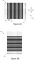
- FIG 2A illustrates asymmetric imaging of a grating target portion 200 caused by scanning in an X direction (specifically, in a west and east direction) with a charged particle beam.
- a charged particle beam is raster scanned in a scan pattern 202 that is in an "east" direction relative to the lines of the target 200.
- the beam scans along a plurality of scan paths 202 that are each in a direction that is perpendicular to the line structures of the grating target 200.
- Figure 2B illustrates similar asymmetric imaging of a grating target 250 that is caused by scanning in a single Y (or south) direction with a charged particle beam.
- the line structures asymmetrically retain charge from the charged particle beam as it scans across the line structures and, as a result, the periodic line image is asymmetric.
- leading edge 204a of line 204 may have a thicker white edge in the resulting image than the trailing edge 204b of the same line 204. This asymmetry may be caused by uneven positive charging of the line edges as the beam moves across such lines, which results in unequal amounts of secondary electrons from the different edges reaching the detector and contributing to the image.
- Certain embodiments of the present invention provide symmetric scanning patterns that result in symmetric charging effects for the image generated for the sample, which also results in symmetric PR damage.
- a charged particle beam e.g., e-beam
- Figure 2C illustrates a process for symmetrically scanning the charged particle beam back across a Y direction grating target in a direction that is opposite of the charged particle beam scan illustrated in Figure 2B to result in target image 260.
- e-beam scans 254 will tend to result in asymmetry between the leading and lagging edges in the target image 260, which is opposite the asymmetry in the target image 250 that is caused by asymmetric beam scans 252 as shown in Figure 2B .
- Combining images from the bidirectional (opposite or symmetrical) scans will tend to result in symmetrical charging effects in the combined image.
- Figure 2D illustrates a scanning pattern that includes symmetrical beam scans that are perpendicular to the Y direction grating structures, which can be used to form a symmetric combined target image 270 in accordance with one embodiment of the present invention.
- a charged particle beam is scanned symmetrically in both a "north" direction (up) and a “south” direction (down) with respect to the longitudinal axis of each line in the grating that is oriented in an east and west direction.
- a similar technique can be implemented with respect to an X direction overlay target.
- the target image 200 of Figure 2A was obtained from grating lines that each have a north and south aligned longitudinal axis.
- a beam may also be scanned in a west direction that is opposite the east-direction beam scan 202 to thereby achieve symmetrical east and west direction scans relative to the overlay target grating 200.
- the images from the symmetric scans (east and west) may then be combined to form a symmetric image.
- e-beam patterns that scan in both +X and -X (east and west) directions or in both +Y and -Y (north and south) directions can be used to form combined symmetric target images for X and Y direction grating structures, respectively.
- the asymmetries in the two different images that were formed by the two directional, but symmetrical, scans may then be combined to form a symmetric image.
- the symmetric image may then be analyzed for accurate overlay (or other measurements, such as CD) determination.
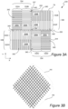
- FIG. 3A is a top plan view of a combination XY overlay mark 330 for which an alternate symmetric beam scan pattern may be implemented in accordance with a specific embodiments of the present invention as described further below.
- the overlay mark 330 of Figure 3A is configured to measure overlay in two separate directions. As such, mark 330 obviates the need to have one mark for each direction in which overlay needs to be measured.
- Overlay mark 330 is shown in a configuration that results when the tested layers of a wafer are in perfect alignment.
- the overlay mark 330 is generally provided to determine the relative shift between two or more successive layers of a wafer or between two or more separately generated patterns on a single layer of a wafer.
- the overlay mark 330 will be described in context of measuring overlay between different layers of a substrate. It should be noted, however, that the overlay mark in this figure (or any other target described herein) may also be used to measure two or more separately generated patterns on a single layer of a substrate.
- the overlay mark 330 includes a plurality of working zones 332 for determining the registration error between two wafer layers in two different directions.
- the overlay mark 330 includes eight rectangular shaped working zones 332, which are configured to substantially fill its perimeter 79.
- the working zones 332 represent the actual areas of the mark that are used to calculate alignment between different layers of the wafer.
- the working zones 332 are spatially separated from one another so that they do not overlap portions of an adjacent working zone. In this particular configuration, some of the working zones are separated via exclusion zones while other working zones are positioned next to an adjacent working zone.
- working zone 332B is separated from working zones 332E and 332F via an exclusion zone 333 while working zones 332E and 332F are positioned next to one another at their edges without an exclusionary zone there between.
- the working zones 332 are grouped into a first working group 334 and a second working group 336.
- the first working group 334 includes four working zones 332A-D that are configured to provide overlay information in a first direction.
- the first direction may be the Y direction.
- two of them 332A and 332D are disposed in the first layer and two of them 332B and 332C are disposed in the second layer (the first layer is represented by cross hatching, the second layer is represented by no cross hatching).
- the centers of symmetry 335 of working zones 332A&D and working zones 332B&C coincide exactly.
- the second working group 336 includes four working zones 332E-H configured to provide overlay information in a second direction that is perpendicular to the first direction.
- the second direction may be the X direction.
- the centers of symmetry 337 of working zones 332E&H and working zones 332F&G coincide exactly.
- the centers of symmetry may also be offset by a predefined amount and a deviation from such predefined offset indicates an overlay error.
- each of the groups 334 and 336 represents an "X" - configured mark (albeit offset).
- working group 334 includes working zones 332A&D, which are on the same first layer and in diagonally opposed positions relative to one another, and working zones 332B&C, which are on the same second layer and in diagonally opposed positions relative to one another.
- working zones 332A&D are angled relative to working zones 3322B&C.
- working zone 332A is spatially offset from working zone 332D
- working zone 332B is spatially offset from working zone 332D.
- working group 336 includes working zones 332E&H, which are on the same first layer and in diagonally opposed positions relative to one another, and working zones 332F&G, which are on the same second layer and in diagonally opposed positions relative to one another. Further, working zones 332E&H are angled relative to working zones 332F&G. Further still, working zone 332E is spatially offset from working zone 332H, and working zone 332F is spatially offset from working zone 332G. In essence, this particular mark produces two "X" configured marks that are positioned orthogonal to each other, i.e., working group 394 and working group 396.
- a working zone on one layer is generally juxtaposed relative to a working zone on another layer.
- working zone 332A is juxtaposed relative to working zone 332B and working zone 332C is juxtaposed relative to working zone 332D.
- working zone 332E is juxtaposed relative to working zone 332H and working zone 332F is juxtaposed relative to working zone 332G.
- the working zone on the second layer is typically positioned closer to the center than the working zone on the first layer.
- working zones 332B and 332C and working zones 332F and 332G are positioned closer to the center 342 of the region of interest 344 than their juxtaposed working zones 332A and 332D and working zones 332E and 332H, respectively.
- the juxtaposed pairs are positioned in an opposed relationship (e.g., diagonal) relative to the other juxtaposed pair in the group.
- juxtaposed pairs 332A&B are positioned opposite juxtaposed pairs 332C&D
- juxtaposed pairs 332E&F are positioned opposite juxtaposed pairs 332G&H.
- the configuration of the working zones is rotationally symmetric (+90, 180, 270, 360 degrees around the center of the mark). This is typically done to reduce the impact of radial and axial variations across the field of view of the metrology tool, as for example, radial and axial variations caused by non-uniform optical aberrations and illumination that may cause tool induced shifts (TIS).
- Radial variations generally refer to variations that radiate from the center of the mark to the outer regions of the mark.
- Axial variations generally refer to variations that occur in directions along the axis of the mark, as for example, in the X direction from the left to the right portions of the mark, and in the Y direction from the lower to the upper portions of the mark.
- Each of the working zones 332A-H includes a periodic structure 338 comprised of a plurality of coarsely segmented lines 340.
- the linewidths, D, and spacings, s, of the coarsely segmented lines may be widely varied.
- each of the periodic structures 338 substantially fills the perimeter of its corresponding working zone 332.
- the periodic structures 338 are also disposed on the layer of its corresponding working zone 332.
- the periodic structures 338 may be broken up into a first periodic structure 338A that is associated with the first working group 334 and a second periodic structure 338B that is associated with the second working group.
- the first periodic structures 338A are all oriented in the same direction, i.e., the coarsely segmented lines 340 are parallel and horizontally positioned relative to each other.
- the second periodic structures 338B are also all oriented in the same direction (albeit differently than the first periodic structures), i.e., the coarsely segmented lines 340 are parallel and vertically positioned relative to each other.
- the periodic structures 338A in the first working group 334 are orthogonal to the periodic structures 338B in the second working group 336.
- the coarsely segmented lines of juxtaposed periodic structures are aligned with one another, ( e.g ., if we ignore the different layers, they appear to be continuous gratings).
- the coarsely segmented lines of working zone 332A may align with the coarsely segmented lines of working zone 332B and coarsely segmented lines of working zone 332C may align with the coarsely segmented lines of working zone 332D.
- the coarsely segmented lines of working zone 332E may align with the coarsely segmented lines of working zone 332F and coarsely segmented lines of working zone 332G may align with the coarsely segmented lines of working zone 332H.
- a symmetrical X or Y beam scan pattern would result in the e-beam being scanned along at least a portion of the target lines' longitudinal axis, which is generally avoided.
- an e-beam that is scanned bi-directionally along the X axis (east and west) would form scan paths that are perpendicular to the vertical lines of the second working group 336 and parallel with the horizontal lines of the first second working group 334.
- an e-beam that is scanned bi-directionally in the Y direction would form scan paths that were perpendicular to the horizontal lines of the first working group 334 and parallel to the vertical lines of the second working group 336.
- certain embodiments of the present invention include charged particle beam scan patterns that form symmetrical scan paths having angles with respect to the scanned edges that are at least 10° or in a range between about 10° and 80° from any of the lines of the target.
- the scan paths may include pairs of scan paths at multiple rotations so as to maximize the symmetry in the final combined image.
- Figure 3B illustrates an alternative beam scan pattern having symmetric scan paths that are 45° with respect to a combination XY target having both X and Y lines ( e.g ., target 330 of Figure 3A ) in accordance with a specific implementation of the present invention.
- multiple pairs of bi-directional line scans at two different rotations (or 4 different scan angles) symmetrically cover the target.
- FIG. 3C is a flowchart illustrating a general procedure 350 for determining overlay with symmetric beam scanning in accordance with one embodiment of the present invention.
- a periodic target for measuring overlay in at least one direction is provided in operation 352 of Figure 3C .
- the target may include structures for only measuring overlay in a single direction (e . g ., X or Y) or a target that includes structures for measuring overlay in two or more directions ( e . g ., X and Y), like the XY target 330 of Figure 3A .
- a charged particle beam may then be scanned in a first direction across a plurality of scan swaths of the target and at a first tilt with respect to the target so that each scanned edge of the target is scanned at an angle in operation 354. Additionally, the charged particle beam can then be scanned in a second direction, which is opposite the first direction, across the same plurality of scan swaths and at a second tilt that is 180° from the first tilt in operation 356.
- the pattern of scans may include either scanning in north and south directions or scanning in east and west directions, respectively, across a plurality of scanned swaths
- the scanning operations may be repeated at new tilts so as to achieve symmetry in the scans with respect to the target.
- the beam is scanned with respect to the target along sets of bidirectional swaths at tilts of 45°, 135°, 225°, and 315°. That is, scanned swaths for each first pair 342 are at 45°and 225°, and scan swaths of each second pair 344 are at 135°and 315°.
- These scan swaths may be achieved by scanning the charged particle beam in two translational directions while the target is moved in a translational and rotational manner.
- the target is moved in a linear and rotational manner under the charged particle beam so as to scan the target in four frames.
- the target is moved perpendicular to the beam's scan direction so as to scan a first set of swaths in a first direction and at a first tilt ( e.g ., 45°).
- the target may then be rotated to a second tilt (e.g ., 225°), which is 180° from the first tilt, so that the beam will effectively scan in a second opposite direction with respect to the first set of swaths.
- the target is then translated in a direction that is perpendicular to the beam's scan direction so as to scan the same first set of swaths in the second direction that is opposite the first direction. This process may then be repeated for the other two tilt pair 135°and 315°.
- the charged particle may be scanned in two opposite linear directions, and the target may be rotated to only two tilt positions for such bidirectional beam scans.
- the target is translated under the beam in a direction that is perpendicular to the beam scan's direction so as to raster scan multiple lines in the beam's direction.
- the target may be rotated and translated with respect to the charged particle beam so that the beam scans across a plurality of lines/swaths in two directions and at a first pair of tilts 45°and 225° with respect to the target.
- the target is then rotated once more, and the target is translated so that the beam then scans across a plurality of lines/swaths in two directions and at a second pair of tilts 135°and 315° with respect to the target.
- Symmetric charged particle scan patterns may likely result in improvements for the edge sharpness and symmetry for a wide variety of target configurations, such as an XY overlay target.
- the beam is only scanned in opposite directions along either scan swaths 342 or scan swaths 344, with or without rotating the target to achieve the two symmetric directions along the same scan swaths.
- each sequential scan may skip swaths (or lines) in accordance with an alternative embodiment of the present invention.
- Figure 3D is a diagrammatic representation of a symmetric scanning process that includes skipping lines in accordance with an alternative embodiment of the present invention.
- the scan pattern 374 includes sequentially scanned lines that skip swaths or lines. For example, 8 lines are skipped between each sequential swath scan.
- the scan pattern would also include scans in the opposite direction (from right to left) that trace over the illustrated scan lines 374.
- the skipped lines would be left unscanned, and overlay may be determined based on a combination of the signals or images that are generated in response to the beam moving across each of the scanned lines 374 in two opposite symmetrical directions. For example, symmetric image portions obtained in response to the scanned lines 374 are combined to form a combination image that excludes image data from skipped lines of the target.
- any suitable number of lines may be skipped so as to minimize damage to the scanned material and obtain enough data for accurately determining overlay or the like.
- a scan pattern that skips lines causes less damage to certain materials such as photoresist, which tends to shrink in areas that are scanned by a charged particle beam.
- the number of skipped lines may be selected so that the amount of shrinkage will tend to be comparable to line edge roughness and not significantly affect the overall line edges.
- 8 or more lines are skipped.
- 100 or more lines are skipped, for example, for an 8k by 8k field of view (FOV).
- each swath scan results in generation of signals or images, for example, by the system's detector and processor system.
- the images from the first and second direction scans may then be combined into a combined image in operation 358.
- Figure 2D shows a representation of a combined image for a Y direction target portion in which no lines are skipped. If lines are skipped, the image portions for the individually scanned lines may be compressed together so that they abut each other in the combined image. If 8 lines are skipped by way of example, the resulting combined image will be 1/8 the size of an image that is formed without skipping lines.
- images are combined as each pair of scanned swaths of the target are collected.
- images may be combined after the images for all of the pairs of swaths for a particular overlay direction are collected or after the images for all pairs of swaths for all overlay directions are collected.
- the combined image may then be analyzed to determine overlay (or another characteristic, such as CD) in operation 360.
- Each combined image for each scan swath may be analyzed separately or a single combined image for all the swaths may be analyzed.
- a subsequent process is adjusted to compensate for the process that is out of specification in operation 364. For example, if it is determined that the photoresist pattern is misaligned in any portion, the photoresist may then be stripped and reapplied in a corrected pattern to eliminate the misalignment.
- the subsequent process is then performed so as to continue fabrication of the same wafer in operation 366. For example, the wafer may be patterned.
- processing of the wafer may be halted and the wafer may then be discarded in operation 368.
- the process that is out of specification may then be adjusted for subsequent wafers in operation 369.
- Figure 3E is a flow chart illustrating the operation 362 of Figure 3C for determining whether a target is out of specification in accordance with a specific implementation of the present invention. Although this procedure is described with respect to a target having structures with a 180° rotational COS, of course, this procedure may be easily modified for structures with mirror or other type of symmetry.
- the center of the imaged target structures are initially moved to the center of the FOV of the inspection tool in operation 382.
- the region of interests (ROI's) of each layer are then determined in operation 384.
- the X target structures of Figure 1 will be used to illustrate the procedure of Figure 3E .
- four ROI's may be formed for the X direction target structures 106a, 106b, 108a and 108b of Figure 1 , as represented by the dotted lines.
- the dotted line 102 may represent the FOV of the inspection tool, while the cross 110 represents the center of the X target structures.
- the COS for each set of structures 106 and 108 from the first and second layers, respectively, may be determined using any suitable technique.
- an edge technique may be utilized to determine COS for the structures in each layer.
- the outside edges of each ROI of each layer are used to determine the COS for each layer in operation 386.
- the outside edges of each ROI may be determined and then the edges are then used to find a center position between the outside edges of each set of structures (e.g., between structures 106a and structures 106b).
- each set of sub-resolution lines e.g., fine lines 404 that form part of each course set of lines 402
- the edge of each set of sub-resolution lines would be measured as a single edge.
- COS determination technique is referred to as the correlation technique.
- an initial COS position is estimated between the ROI's of the structures of each layer in operation 388.
- an initial estimate of COS 110 may be positioned between structures 106a and 106b.
- Two linear arrays are then obtained by measuring across the two sets of structures at positions that are equal distances from the initial COS.
- the structures 106a and 106b will tend to each result in a periodic signal with three peak intensity values.
- the two obtained linear arrays are then flipped horizontally and vertically and matched and a metric of correlation such as the product is calculated.
- the arrays are moved with respect to one another and the metric is calculated for each offset.
- the metric is then plotted and the correct COS is located by finding the maximum of the correlation metric.
- Intelligent searching algorithms e.g., a binary search
- Intelligent searching algorithms may also be used to efficiently locate the correct COS position.
- the COS is found using any suitable technique, it is then determined whether the COS of the first layer structures differs from the COS of the second layer structures by more than a predetermined value in operation 394. If they do not differ by more than the predetermined value, it is determined that the target under analysis in not out of specification in operation 398. However, if they do differ by more than the predetermined amount, it is determined that the target under analysis is out of specification in operation 396. The procedure for determining whether the target is out of specification then ends.
- Opposite direction and tilted (with respect to the overlay direction or longitudinal axis of the target lines) scan patterns may be applied to any suitable type of combination X and Y targets, besides the example of Figure 3A .
- Several periodic overlay targets are further described in U.S. Patent No. 9,702,693, issued 11 July 2017 by Ghinovker et al. , which patent is incorporated herein by reference.
- Figures 4A through 4I illustrate a plurality of different combination XY targets for which symmetric beam scanning techniques may be implemented in accordance with various embodiments of the present invention.
- Figure 4A is a top plan view of another multi-directional overlay mark 400.
- the coarsely segmented lines 402 are formed by a plurality of finely segmented elements 404.
- FIG 4B is a top plan view of an overlay mark 410, in accordance with an alternate target.
- the overlay mark 410 may generally include X and Y line gratings with the addition of a box in box overlay structure 418.
- overlay mark 410 contains eight working zones 412A-H for determining the registration error between two wafer layers in two different directions (one layer is represented by cross-hatching, the other is not).
- Each of the working zones includes a periodic structure 414 comprised of a plurality of coarsely segmented lines 416.
- the working zones 412 are arranged to accommodate additional structure 418 in the center of the mark 410.
- the working zones 412A-H are disposed around the outer region of the mark, while the additional structure 418 is disposed in the center of the mark.
- the additional structure 418 may represent a standard box in box overlay structure.
- Figure 4C is a top plan view of an overlay mark 420, in accordance with an alternate target.
- the overlay mark 420 of Figure 4C is configured to measure overlay in two separate directions.
- the mark 420 includes triangularly shaped working zones 402.
- a first set of working zones 422A-D are configured to provide overlay information in a first direction.
- the first direction may be the Y direction.
- two of them 422A and D are disposed in the first layer and two of them 422 B and 422C are disposed in the second layer.
- the centers of symmetry 425 of working zones 422A&D and working zones 422B&C coincide exactly.
- a second set of working zones 422E-H are configured to provide overlay information in a second direction that is perpendicular to the first direction.
- the second direction may be the X direction.
- each of the working zones 422E-H includes a periodic structure 428 comprised by a plurality of coarsely segmented lines 421. Although not shown, each coarsely segmented line may be formed by a plurality of finely segmented elements to further enhance this mark or any mark described herein.
- Figure 4D is a top plan view of an overlay mark 430, in accordance with an alternative target.
- mark 430 has the same general layout and characteristics as mark 420 of Figure 4C , i.e., eight triangularly shaped working zones.
- Mark 430 differs from mark 420, however, in that it biases the center of the mark with a grating pattern 432 formed on one of the two layers.
- the grating pattern 432 is typically used in cases where the mark quality in one layer is poorer than the mark quality in the other layer due to contrast or graininess. That is, the information (e.g., edges) in a layer where contrast is low is increased.
- biasing the center of the FOV with one layer may further protect it from process damage.
- the grating pattern 432 may be widely varied.
- grating pattern may include any number of lines in any number of distributions and sizes.
- the grating pattern is formed on the second layer and includes groups of two coarsely segmented lines 434 that alternate in direction (e.g., X and Y directions) around the center of the mark.
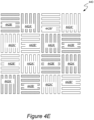
- FIG 4E is a top plan view of an overlay mark 440, in accordance with an alternate target.
- overlay mark 440 is configured to measure overlay in two separate directions.
- the overlay mark 440 includes a plurality of working zones 442 for determining the registration error between two wafer layers in two different directions.
- the overlay mark 442 includes sixteen square shaped working zones 442, which are configured to substantially fill its perimeter.
- Each of the working zones 442 includes a periodic structure of coarsely segmented lines. Of the 16 working zones, 8 of the working zones 442A are oriented in the X direction and 8 of the working zones 442B are oriented in the Y direction (as shown by the periodic structures disposed therein). Of the 8 working zones 442, in any given orientation (A or B), 4 of the working zones 442' are printed in a first layer (represented by cross hatching) while 4 of the working zones 442" are printed in a second layer (not represented by cross hatching).
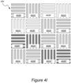
- FIG 4F is a top plan view of an overlay mark 450, in accordance with an alternate target.
- overlay mark 450 is configured to measure overlay in two separate directions.
- the overlay mark 450 includes a plurality of working zones 452 for determining the registration error between two wafer layers in two different directions.
- Each of the working zones 452 includes a periodic structure of coarsely segmented lines.
- 8 of the working zones 452A are oriented in the X direction and 8 of the working zones 452B are oriented in the Y direction (as shown by the periodic structures disposed therein).
- 8 working zones 452 in any given orientation (A or B), 4 of the working zones 452' are printed in a first layer (represented by cross hatching) while 4 of the working zones 452" are printed in a second layer (not represented by cross hatching).
- FIG 4G is a top plan view of an overlay mark 460, in accordance with an alternate target.
- overlay mark 460 is configured to measure overlay in two separate directions.
- the overlay mark 460 includes a plurality of working zones 462 for determining the registration error between two wafer layers in two different directions.
- Each of the working zones 462 includes a periodic structure of coarsely segmented lines.
- 8 of the working zones 462A are oriented in the X direction and 8 of the working zones 462B are oriented in the Y direction (as shown by the periodic structures disposed therein).
- 8 working zones 462 in any given orientation (A or B), 4 of the working zones 462' are printed in a first layer (represented by cross hatching) while 4 of the working zones 462" are printed in a second layer (not represented by cross hatching).
- FIG 4H is a top plan view of an overlay mark 480, in accordance with an alternate structure.
- overlay mark 480 is configured to measure overlay in two separate directions.
- the overlay mark 480 includes a plurality of working zones 482 for determining the registration error between two wafer layers in two different directions.
- Each of the working zones 482 includes a periodic structure of coarsely segmented lines. Of the 16 working zones, 8 of the working zones 482A are oriented in the X direction and 8 of the working zones 482B are oriented in the Y direction (as shown by the periodic structures disposed therein).
- any given orientation (A or B)
- 4 of the working zones 482' are printed in a first layer (represented by cross hatching) while 4 of the working zones 482" are printed in a second layer (not represented by cross hatching).
- 4 of the working zones 482 in any given orientation (A or B), 4 of the working zones 482 have a periodic structure M with a first period (represented by thinner lines) while 4 of the working zones 482 have a periodic structure N with a second period that is different than the first period (represented by wider lines).
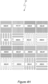
- Figure 4I is a top plan view of an overlay mark 490, in accordance with an alternate structure.
- overlay mark 490 is configured to measure overlay in two separate directions.
- overlay mark 490 is also configured to determine the relative shift between three successive layers of a wafer or between three separately generated patterns on a single layer of a wafer.
- the overlay mark 490 includes sixteen square shaped working zones 492.
- Each of the working zones 492 includes a periodic structure of coarsely segmented lines.
- the first layer (also represented by a single prime) is disposed over the second layer (also represented by a double prime) and the second layer is disposed over the third layer (also represented by a triple prime).
- the first layer may represent a resist layer
- the second layer may represent a first metal layer
- the third layer may represent a second metal layer.
- FIG. 5 is a top plan view of an alternative combination XY overlay mark 500 having overlapping periodic line structures for which symmetric beam scan techniques may be implemented in accordance with specific embodiments of the present invention.
- This target 500 includes complex patterns of sub-resolution X and Y features, with some of the X structures interleaved with the Y structures.
- working group 502A contains interleaved X and Y sub-resolution features for a first layer as shown in expanded area 501.
- Some of the working zones also include an overlaid working zone for a second layer that is formed after and on top of the first layer.
- working zone 502B contains X and Y sub-resolution periodic features in the first layer with a second layer of X course periodic structures formed over the first layer periodic structures.
- Overlay may generally be determined by the difference between centers of symmetry/gravity of the currently formed layer patterns and previous layer patterns.
- Figure 6 is another target 600 having XY overlay structures for which symmetric beam scan techniques may be implemented in accordance with specific embodiments of the present invention.
- working group 602A contains Y overlay grating structures in three different layers (white, black and cross-hashing), while working group 602B contains X overlay grating structures in the same three different layers (white, black, and cross-hatching).
- the structures for each layer in each working group are arranged to have a same center position 604 when there is zero overlay error.
- Overlay may generally be determined by the difference between centers of gravity (or deviation from predefined offset between centers of gravity) of the currently formed layer patterns and previous layer patterns.
- a scan pattern may generally include tilted bidirectional scans with respect to the line edges and symmetrical with respect to the target, with or without skipping lines in between sequential scans.
- the beam may be scanned with respect to combination XY target along sets of swaths that are tilted at 45°, 135°, 225°, and 315° or any suitable combination of symmetrical angles that are tilted with respect to the overlay target's orientation.
- the tilt angles can include 19° to 21° and 199° to 201° so the e-beam can scan perpendicular to the top layer pattern (e.g., 701) in Figure 7 .
- FIG. 7 is a top plan view of an alternative target portion 700 having periodic line structures in different layers and directions that are tilted with respect to each other at an angle that excludes a perpendicular or parallel angle. That is, the tilt angle between the two gratings is greater than 0° and less than 90°.
- the target has a set of lines in a first layer, which are denoted by cross-hatched shading, and a set of lines in a second layer, which are denoted by white shading.
- the second layer lines are tilted with respect to the first layer lines at an angle that is about 21°.
- the charged particle beam can be scanned in pairs of symmetrical scans at any suitable symmetrical combination of tilted angles.
- Each pair of scans include two opposite directional set of scans that are symmetrical with respect to each other, and the resulting scan paths of all scan pairs are not parallel to any longitudinal axis of the target.
- the beam scan pattern may include scans that are either perpendicular to each of the line sets or tilted with respect to each of the line sets.
- the charged particle beam would not be scanned in east and west directions since this would result in the horizontal lines of the second layer being scanned along their longitudinal axis.
- Overlay for the target of Figure 7 may generally be determined by the difference between centers of gravity of the currently formed layer patterns and previous layer patterns.
- FIG. 8 is a top plan view of an alternative overlay mark 810 formed from a plurality of contact structures for which X and Y overlay may be determined.
- the overlay mark 810 is configured to measure overlay in two separate directions. As such, mark 810 obviates the need to have separately positioned or offset structures for each X and Y direction in which overlay is to be measured.
- Overlay mark 810 is shown in a configuration that results when the tested layers of a wafer are in perfect alignment.
- the overlay mark 810 includes a plurality of working zones 812 for determining the registration error between two wafer layers in two different directions.
- the overlay mark 810 includes four square shaped working zones 812, which are configured to substantially fill a field of view (not shown) of the metrology tool used to image the overlay mark 810.
- the working zones 812 represent the actual areas of the mark that are used to calculate alignment between different layers of the wafer. As mentioned previously, the working zones 812 are spatially separated from one another so that they do not overlap portions of an adjacent working zone of the second layer.
- the working zones are configured to provide overlay information in two directions, as for example, in the X and Y directions.
- two of them 812A and 812D are disposed in the first layer and two of them 812B and 812C are disposed in the second layer (the first layer is represented by solid fill, the second layer is represented by no fill).
- Working zones 812A and 812D which are disposed on the same first layer, are positioned opposite one another at a first vertical angle while working zones 812B and 812C, which are disposed on the same second layer, are positioned opposite one another at a second vertical angle (e.g., diagonally).
- These cross-positioned structures form an "X" shaped pattern.
- Each of the working zones 812 contains an individual periodic structure 814, as for example, periodic structures 814A-D. As shown, each of the periodic structures 814 substantially fills the perimeter of its corresponding working zone 812. As should be appreciated, each of the periodic structures 814 is formed in the layer of its corresponding working zone 812.
- the periodic structures 814 include coarsely segmented elements 816 that are arranged in spaced apart rows and columns.
- each of the coarsely segmented elements 816 may also be formed by finely segmented elements 818.
- the finely segmented elements 818 are also arranged in spaced apart rows and columns.
- the individual coarsely segmented elements 816 and finely segmented elements 818 may be configured with a variety of sizes, shapes and distributions.
- both the coarsely segmented elements 816 and finely segmented elements 818 are square shaped and equally spaced from an adjacent element.
- overlay mark 810 can be used to measure the misregistration value in two separate directions that are perpendicular to each other since the mark 810 has the same repeating structural pattern in orthogonal directions.
- the overlay contact array target 810 may be scanned in north, south, east, and west directions, only north and south directions (for Y overlay), or only eat and west directions (for X overlay). Any scan pattern may include skipping lines.
- the target may include an array of cross-shaped structures. In this later example, the beam may be scanned at tilted angles with respect to the target, like the combination XY targets described herein.
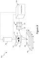
- FIG. 9 is a diagrammatic representation of a scanning electron microscopy (SEM) overlay metrology system in accordance with one embodiment of the present invention. Scanning in symmetrical directions across the periodic structures may avoid image asymmetries caused by buildup of electrons, and as a result, minimize inaccurate overlay measurements (or the like).
- SEM scanning electron microscopy
- the system 900 may include, but is not limited to, a defect-review (DR) SEM tool with SEM overlay option, a critical-dimension (CD) SEM tool with SEM overlay option, a standalone SEM tool, a lithography/etch tool with integrated SEM overlay metrology, or a lithography/etch metrology cluster with features such as imaging optical overlay, scatterometry optical overlay, scatterometry CD, and CDSEM with SEM overlay option.
- DR defect-review
- CD critical-dimension
- the system 900 may be configured to scan a sample 906 such as, but not limited to, a wafer (e.g., semiconductor wafer) having two or more layers formed thereon with an electron beam 904 in order to determine overlay error (e.g., a misalignment or spatial offset between at least two layers of interest).
- a sample 906 such as, but not limited to, a wafer (e.g., semiconductor wafer) having two or more layers formed thereon with an electron beam 904 in order to determine overlay error (e.g., a misalignment or spatial offset between at least two layers of interest).
- the system 900 may operate in any scanning mode known in the art.
- the system 900 may operate in a swathing mode when scanning an electron beam 904 across the surface of the sample 906.
- the system 900 may scan an electron beam 904 across the sample 906, while the sample is moving, with the direction of scanning being nominally perpendicular to the direction of the sample motion.
- the system 900 may operate in a step-and-scan mode when scanning an electron beam 904 across the surface of the sample 906.
- the system 900 may scan an electron beam 904 across the sample 906, which is nominally stationary when the beam 904 is being scanned.
- the system 900 may include an electron beam source 902 for generating one or more electron beams 904.
- the electron beam source 902 may include any electron source known in the art.
- the electron beam source 902 may include, but is not limited to, one or more electron guns.
- a computing system 924 or controller may be communicatively coupled to the electron beam source 902.
- the computing system 924 may be configured to adjust one or more electron source parameters via a control signal to the electron beam source 902.
- the computing system 924 may be configured to vary the beam current for the electron beam 904 emitted by source 902 via a control signal transmitted to control circuitry of the electron beam source 902.
- the sample 906 may be disposed on a sample stage 908 configured to support the sample 906 during scanning.
- the sample stage 908 is an actuatable stage.
- the sample stage 908 may include, but is not limited to, one or more translational stages suitable for selectably translating the sample 906 along one or more linear directions (e.g., x-direction, y-direction and/or z-direction).
- the sample stage 908 may include, but is not limited to, one or more rotational stages suitable for selectably rotating the sample 906 along a rotational direction.
- the sample stage 908 may include, but is not limited to, a rotational stage and a translational stage suitable for selectably translating the sample along a linear direction and/or rotating the sample 906 along a rotational direction.
- the computing system 924 or controller is communicatively coupled to the sample stage 908.
- the computing system 924 may be configured to adjust one or more stage parameters via a control signal transmitted to the sample stage 908.
- the computing system 924 may be configured to vary the sample scanning speed and/or control the scan direction via a control signal transmitted to control circuitry of the sample stage 908.
- the computing system 924 may be configured to vary the speed and/or control the direction with which sample 906 is linearly translated (e.g., x-direction or y-direction) relative to the electron beam 904.
- the sample 906 may be scanned in a tilted orientation relative to feature placement (e.g., perpendicular or tilted otherwise with respect to a longitudinal axis of the pattern lines) of target structures forming an overlay metrology target or mark on the sample 906.
- feature placement e.g., perpendicular or tilted otherwise with respect to a longitudinal axis of the pattern lines
- the system 900 may further include a set of electron-optic elements 910.
- the set of electron-optics may include any electron-optic elements known in the art suitable for focusing and/or directing the electron beam 904 onto a selected portion of the sample 906.
- the set of electron-optics elements includes one or more electron-optic lenses.
- the electron-optic lenses may include, but are not limited to, one or more condenser lenses 912 for collecting electrons from the electron beam source.
- the electron-optic lenses may include, but are not limited to, one or more objective lenses 914 for focusing the electron beam 904 onto a selected region of the sample 906.
- the electron beam 904 may be directed to the sample 906 at a controlled angle to the sample grating. Because wafer system of coordinates does not necessarily coincide with SEM system of coordinates, controlling a fine scan angle may improve matching between the coordinate systems and significantly contribute to sampling performance/accuracy.
- the set of electron-optics elements includes one or more electron beam scanning elements 916.
- the one or more electron beam scanning elements 916 may include, but are not limited to, one or more scanning coils or deflectors suitable for controlling a position of the beam relative to the surface of the sample 906.
- the one or more scanning elements 916 may be utilized to scan the electron beam 904 across the sample 906 in a selected scan direction or pattern.
- the sample 906 may be scanned in tilted or perpendicular bidirectional scans relative to feature placement (e.g., at bidirectional directions and angled with respect to target lines) of target structures forming an overlay metrology target or mark on the sample 906.
- the computing system 924 or controller may be communicatively coupled to one or more of the electron-optic elements 910, such as the one or more scanning elements 916. Accordingly, the computing system may be configured to adjust one or more electron-optic parameters and/or control the scan direction via a control signal transmitted to the one or more communicatively coupled electron-optic elements 910.
- the system 900 may further include a detector assembly 918 configured to receive electrons 917 from the sample 906.
- the detector assembly 918 includes an electron collector 920 (e.g., secondary electron collector).
- the detector assembly may further include an energy filter 919 based, for example, on retarding field principle.
- the energy filter 919 may be configured to stop low energy secondary electrons while passing high energy secondary electrons (i.e., backscattered electrons). If the energy filter 919 is not activated, all secondary electrons are detected according to collection efficiency of the detection system. By subtracting high energy electron image from overall electron image, low energy secondary electron image can be obtained.
- the detector assembly 918 may further include a detector 922 (e.g., scintillating element and PMT detector 922) for detecting electrons from the sample surface (e.g., secondary electrons).
- the detection system 922 may include several electron detectors, such as, for example, one or more Bright Field (BF) detectors 921 and one or more Dark Field (DF) detectors 923. In some embodiments, there may be from 2 to 8 (or even more) DF detectors 923.
- the BF detector 921 detects electrons with low (according to wafer normal) emission angles, while DF detectors 923 provide information carried by the electrons with higher emission angles.
- the detector 922 of the detector assembly 918 includes a light detector.
- the anode of a PMT detector of the detector 922 may include a phosphor anode, which is energized by the cascaded electrons of the PMT detector absorbed by the anode and may subsequently emit light.
- the light detector may collect light emitted by the phosphor anode in order to image the sample 906.
- the light detector may include any light detector known in the art, such as, but not limited to, a CCD detector or a CCD-TDI detector.
- the system 900 may include additional/alternative detector types such as, but not limited to, Everhart-Thornley type detectors.
- the embodiments described herein are applicable to single detector and multiple-detector arrangements.
- the computing system 924 or controller is communicatively coupled to the detector assembly 918.
- the computing system 924 may be configured to adjust one or more image forming parameters via a control signal transmitted to the detector assembly 918.
- the computing system may be configured to adjust the extraction voltage or the extraction field strength for the secondary electrons.
- the computing system 924" may include one or more computing systems or controllers, such as one or more processors configured to execute one or more instruction sets embedded in program instructions stored by at least one non-transitory signal bearing medium.
- the computing system 924 may control various scanning or sampling parameters such as, but not limited to, those described herein.
- the detector assembly 918 may include any device or combination of devices known in the art for characterizing a sample surface or bulk with an electron beam 904.
- the detector assembly 918 may include any particle detector known in the art configured to collect backscattered electrons, Auger electrons, transmitted electrons or photons (e.g., x-rays emitted by surface in response to incident electrons).
- the detected electrons are differentiated (e.g., secondary electrons vs. backscattered electrons) based upon the energy levels and/or emission angles of the detected electrons, and by subtracting high energy electron image from overall electron image, low energy secondary electron image can be obtained.
- the computing system 924 may be configured to receive and/or acquire data or information (e.g., detected signals/images, statistical results, reference or calibration data, training data, models, extracted features or transformation results, transformed datasets, curve fittings, qualitative and quantitative results, etc.) from other systems by a transmission medium that may include wireline and/or wireless portions.
- the transmission medium may serve as a data link between the computing system 924 and other systems (e.g., memory on-board metrology system, external memory, reference measurement source, or other external systems).
- computing system 924 may be configured to receive measurement data from a storage medium (e.g., internal or external memory) via a data link.
- results obtained using the detection system may be stored in a permanent or semipermanent memory device (e.g., internal or external memory).
- the results may be imported from on-board memory or from an external memory system.
- the computing system 924 may send data to other systems via a transmission medium.
- qualitative and/or quantitative results, such as overlay values, determined by computing system 924 may be communicated and stored in an external memory.
- measurement results may be exported to another system.
- Computing system 924 may include, but is not limited to, a personal computer system, mainframe computer system, workstation, image computer, parallel processor, or any other device known in the art.
- the term "computing system” may be broadly defined to encompass any device having one or more processors, which execute instructions from a memory medium.
- Program instructions may be stored in a computer readable medium (e.g., memory).
- Exemplary computer-readable media include read-only memory, a random access memory, a magnetic or optical disk, or a magnetic tape.
- the metrology tool may be designed to make many different types of measurements related to semiconductor manufacturing. Certain embodiments of the invention for determining quality and/or quantitative values may utilize such measurements. Additional metrology techniques for determining specific target characteristics may also be combined with the above-described quality determination techniques. For example, in certain embodiments the tool may obtain signals/images and determine characteristics of one or more targets (e . g ., overlay, critical dimensions, sidewall angles, film thicknesses, process-related parameters (e.g., focus and/or dose).
- the targets can include certain regions of interest that are periodic in nature, such as for example gratings in a memory die. Targets can include multiple layers (or films) whose thicknesses can be measured by the metrology tool.
- Targets can include target designs placed (or already existing) on the semiconductor wafer for use, e.g., with alignment and/or overlay registration operations. Certain targets can be located at various places on the semiconductor wafer. For example, targets can be located within the scribe lines (e.g., between dies) and/or located in the die itself. In certain embodiments, multiple targets are measured (at the same time or at differing times) by the same or multiple metrology tools. The data from such measurements may be combined. Data from the metrology tool may be used in the semiconductor manufacturing process, for example, to feed-forward, feed-backward and/or feed-sideways corrections to the process (e.g. lithography, etch) and therefore, might yield a complete process control solution.
- the process e.g. lithography, etch
- Computational algorithms are usually optimized for metrology applications with one or more approaches being used such as design and implementation of computational hardware, parallelization, distribution of computation, load-balancing, multi-service support, dynamic load optimization, etc. Different implementations of algorithms can be done in firmware, software, FPGA, programmable optics components, etc.
- Certain embodiments of the present invention presented here generally address the field of semiconductor metrology and process control, and are not limited to the hardware, algorithm/software implementations and architectures, and use cases summarized above.
Landscapes
- Physics & Mathematics (AREA)
- General Physics & Mathematics (AREA)
- Chemical & Material Sciences (AREA)
- Analytical Chemistry (AREA)
- Electromagnetism (AREA)
- Engineering & Computer Science (AREA)
- Computer Vision & Pattern Recognition (AREA)
- Exposure And Positioning Against Photoresist Photosensitive Materials (AREA)
- Testing Or Measuring Of Semiconductors Or The Like (AREA)
- Length-Measuring Devices Using Wave Or Particle Radiation (AREA)
- Analysing Materials By The Use Of Radiation (AREA)
Applications Claiming Priority (3)
| Application Number | Priority Date | Filing Date | Title |
|---|---|---|---|
| US201862639603P | 2018-03-07 | 2018-03-07 | |
| US15/969,158 US10446367B2 (en) | 2018-03-07 | 2018-05-02 | Scan strategies to minimize charging effects and radiation damage of charged particle beam metrology system |
| PCT/US2019/020630 WO2019173252A1 (en) | 2018-03-07 | 2019-03-05 | Scan strategies to minimize charging effects and radiation damage of charged particle beam metrology system |
Publications (3)
| Publication Number | Publication Date |
|---|---|
| EP3762779A1 EP3762779A1 (en) | 2021-01-13 |
| EP3762779A4 EP3762779A4 (en) | 2021-12-01 |
| EP3762779B1 true EP3762779B1 (en) | 2025-06-04 |
Family
ID=67843378
Family Applications (1)
| Application Number | Title | Priority Date | Filing Date |
|---|---|---|---|
| EP19764082.4A Active EP3762779B1 (en) | 2018-03-07 | 2019-03-05 | Scan strategies to minimize charging effects and radiation damage of charged particle beam metrology system |
Country Status (8)
| Country | Link |
|---|---|
| US (1) | US10446367B2 (https=) |
| EP (1) | EP3762779B1 (https=) |
| JP (1) | JP7175319B2 (https=) |
| KR (1) | KR102438826B1 (https=) |
| CN (2) | CN121115423A (https=) |
| IL (1) | IL276810B2 (https=) |
| SG (1) | SG11202008092QA (https=) |
| WO (1) | WO2019173252A1 (https=) |
Families Citing this family (19)
| Publication number | Priority date | Publication date | Assignee | Title |
|---|---|---|---|---|
| US11605550B2 (en) * | 2018-12-21 | 2023-03-14 | Xia Tai Xin Semiconductor (Qing Dao) Ltd. | Alignment system |
| JP2021093336A (ja) | 2019-12-12 | 2021-06-17 | 株式会社日立ハイテク | 画像調整方法および荷電粒子ビームシステム |
| US11874102B2 (en) * | 2019-12-30 | 2024-01-16 | Kla Corporation | Thick photo resist layer metrology target |
| KR102857305B1 (ko) * | 2020-02-07 | 2025-09-08 | 케이엘에이 코포레이션 | 반도체 디바이스의 오정합 측정에서의 비직교 타겟 및 이를 사용하기 위한 방법 |
| KR102630496B1 (ko) * | 2020-04-15 | 2024-01-29 | 케이엘에이 코포레이션 | 반도체 디바이스의 오정합을 측정하는 데 유용한 디바이스 스케일 피쳐를 갖는 오정합 타겟 |
| US11054753B1 (en) * | 2020-04-20 | 2021-07-06 | Applied Materials Israel Ltd. | Overlay monitoring |
| KR102608079B1 (ko) * | 2020-05-05 | 2023-11-29 | 케이엘에이 코포레이션 | 고 지형 반도체 스택들에 대한 계측 타겟들 |
| WO2021225587A1 (en) * | 2020-05-06 | 2021-11-11 | Kla Corporation | Inter-step feedforward process control in the manufacture of semiconductor devices |
| US11686576B2 (en) * | 2020-06-04 | 2023-06-27 | Kla Corporation | Metrology target for one-dimensional measurement of periodic misregistration |
| US12100574B2 (en) * | 2020-07-01 | 2024-09-24 | Kla Corporation | Target and algorithm to measure overlay by modeling back scattering electrons on overlapping structures |
| JP7144485B2 (ja) * | 2020-07-15 | 2022-09-29 | 日本電子株式会社 | 像取得方法および電子顕微鏡 |
| US11995848B2 (en) * | 2021-03-22 | 2024-05-28 | Applied Materials Israel Ltd. | Image generation for examination of a semiconductor specimen |
| KR102617622B1 (ko) * | 2021-04-26 | 2023-12-27 | (주)오로스 테크놀로지 | 오버레이 마크 및 이를 이용한 오버레이 계측방법 및 반도체 디바이스 제조방법 |
| KR102750923B1 (ko) * | 2021-06-30 | 2025-01-09 | (주) 오로스테크놀로지 | 오버레이 마크 및 이를 이용한 오버레이 계측방법 및 반도체 디바이스 제조방법 |
| KR102750903B1 (ko) * | 2021-06-30 | 2025-01-09 | (주) 오로스테크놀로지 | 오버레이 마크 및 이를 이용한 오버레이 계측방법 및 반도체 디바이스 제조방법 |
| KR102750914B1 (ko) * | 2021-06-30 | 2025-01-09 | (주) 오로스테크놀로지 | 오버레이 마크 및 이를 이용한 오버레이 계측방법 및 반도체 디바이스 제조방법 |
| US12461456B2 (en) * | 2022-01-28 | 2025-11-04 | Taiwan Semiconductor Manufacturing Company, Ltd. | Method and structure for overlay measurement in semiconductor device manufacturing |
| TW202414771A (zh) * | 2022-09-29 | 2024-04-01 | 聯華電子股份有限公司 | 疊對圖樣 |
| US20240167813A1 (en) * | 2022-11-23 | 2024-05-23 | Kla Corporation | System and method for suppression of tool induced shift in scanning overlay metrology |
Family Cites Families (17)
| Publication number | Priority date | Publication date | Assignee | Title |
|---|---|---|---|---|
| JPH0774079A (ja) * | 1993-09-02 | 1995-03-17 | Nikon Corp | 露光方法及び露光装置 |
| JP3148353B2 (ja) | 1991-05-30 | 2001-03-19 | ケーエルエー・インストルメンツ・コーポレーション | 電子ビーム検査方法とそのシステム |
| JP2000077300A (ja) * | 1998-08-28 | 2000-03-14 | Nikon Corp | 投影露光装置及び位置検出方法 |
| JP2001189263A (ja) | 1999-12-28 | 2001-07-10 | Toshiba Corp | 合わせずれ検査方法及び荷電ビーム露光方法 |
| EP1314198B1 (en) * | 2000-08-30 | 2017-03-08 | KLA-Tencor Corporation | Overlay marks, methods of overlay mark design and methods of overlay measurements |
| US7541201B2 (en) | 2000-08-30 | 2009-06-02 | Kla-Tencor Technologies Corporation | Apparatus and methods for determining overlay of structures having rotational or mirror symmetry |
| US7001830B2 (en) * | 2003-09-02 | 2006-02-21 | Advanced Micro Devices, Inc | System and method of pattern recognition and metrology structure for an X-initiative layout design |
| JP2005183577A (ja) * | 2003-12-18 | 2005-07-07 | Sony Corp | 露光装置、露光方法、および半導体装置の製造方法 |
| JP4734261B2 (ja) * | 2004-02-18 | 2011-07-27 | ケーエルエー−テンカー コーポレイション | 連続変化するオフセットマークと、オーバレイ決定方法 |
| WO2006093722A2 (en) * | 2005-02-25 | 2006-09-08 | Accent Optical Technologies, Inc. | Methods and systems for determining overlay error based on target image symmetry |
| US7808643B2 (en) * | 2005-02-25 | 2010-10-05 | Nanometrics Incorporated | Determining overlay error using an in-chip overlay target |
| DE102008064504B4 (de) * | 2008-12-22 | 2011-04-07 | Carl Zeiss Smt Gmbh | Projektionsbelichtungsverfahren und Projektionsbelichtungsanlage für die Mikrolithographie |
| EP2458441B1 (en) | 2010-11-30 | 2022-01-19 | ASML Netherlands BV | Measuring method, apparatus and substrate |
| JP6002480B2 (ja) * | 2012-07-06 | 2016-10-05 | 株式会社日立ハイテクノロジーズ | オーバーレイ誤差測定装置、及びパターン測定をコンピューターに実行させるコンピュータープログラム |
| US9214317B2 (en) * | 2013-06-04 | 2015-12-15 | Kla-Tencor Corporation | System and method of SEM overlay metrology |
| JP6378927B2 (ja) | 2014-04-25 | 2018-08-22 | 株式会社日立ハイテクノロジーズ | 計測システムおよび計測方法 |
| EP3171396A1 (en) * | 2015-11-18 | 2017-05-24 | Nederlandse Organisatie voor toegepast- natuurwetenschappelijk onderzoek TNO | Method of determining an overlay error, manufacturing method and system for manufacturing of a multilayer semiconductor device, and semiconductor device manufactured thereby |
-
2018
- 2018-05-02 US US15/969,158 patent/US10446367B2/en active Active
-
2019
- 2019-03-05 KR KR1020207028710A patent/KR102438826B1/ko active Active
- 2019-03-05 EP EP19764082.4A patent/EP3762779B1/en active Active
- 2019-03-05 CN CN202511422236.9A patent/CN121115423A/zh active Pending
- 2019-03-05 WO PCT/US2019/020630 patent/WO2019173252A1/en not_active Ceased
- 2019-03-05 JP JP2020546371A patent/JP7175319B2/ja active Active
- 2019-03-05 CN CN201980016988.1A patent/CN111801626A/zh active Pending
- 2019-03-05 SG SG11202008092QA patent/SG11202008092QA/en unknown
-
2020
- 2020-08-19 IL IL276810A patent/IL276810B2/en unknown
Also Published As
| Publication number | Publication date |
|---|---|
| JP2021515232A (ja) | 2021-06-17 |
| CN121115423A (zh) | 2025-12-12 |
| KR102438826B1 (ko) | 2022-08-31 |
| IL276810B2 (en) | 2023-08-01 |
| CN111801626A (zh) | 2020-10-20 |
| JP7175319B2 (ja) | 2022-11-18 |
| WO2019173252A1 (en) | 2019-09-12 |
| EP3762779A1 (en) | 2021-01-13 |
| US20190279841A1 (en) | 2019-09-12 |
| KR20200118908A (ko) | 2020-10-16 |
| IL276810B1 (en) | 2023-04-01 |
| SG11202008092QA (en) | 2020-09-29 |
| US10446367B2 (en) | 2019-10-15 |
| IL276810A (en) | 2020-10-29 |
| EP3762779A4 (en) | 2021-12-01 |
Similar Documents
| Publication | Publication Date | Title |
|---|---|---|
| EP3762779B1 (en) | Scan strategies to minimize charging effects and radiation damage of charged particle beam metrology system | |
| US10417756B2 (en) | Pattern measurement apparatus and defect inspection apparatus | |
| US10762383B2 (en) | Pattern inspection apparatus and pattern inspection method | |
| KR102351677B1 (ko) | 멀티-패터닝 단계 오버레이 오차의 결정 | |
| US6664121B2 (en) | Method and apparatus for position measurement of a pattern formed by a lithographic exposure tool | |
| US10727026B2 (en) | Charged particle beam inspection method | |
| US20150136976A1 (en) | Overlay error measuring device and computer program | |
| US20150029499A1 (en) | Auto-focus system and methods for die-to-die inspection | |
| US6566655B1 (en) | Multi-beam SEM for sidewall imaging | |
| JP6649130B2 (ja) | パターン検査装置及びパターン検査方法 | |
| JP6966319B2 (ja) | マルチビーム画像取得装置及びマルチビーム画像取得方法 | |
| US12205272B2 (en) | Pattern inspection device and pattern inspection method | |
| US20240242334A1 (en) | Method for defect detection in a semiconductor sample in sample images with distortion | |
| TWI773329B (zh) | 圖案檢查裝置以及圖案檢查方法 | |
| US11353413B2 (en) | Mask inspection apparatuses and methods, and methods of fabricating masks including mask inspection methods | |
| US12586753B2 (en) | Image enhancement based on charge accumulation reduction in charged-particle beam inspection | |
| JP2020134165A (ja) | 検査装置及び検査方法 | |
| TWI907989B (zh) | 掃描式電子顯微鏡、掃描式電子顯微鏡系統以及用於實作3d影像演算法的方法 | |
| US20260029725A1 (en) | Localized region of interest based image grabs for improved metrology cost of ownership | |
| KR102765307B1 (ko) | 마스크 검사 장치와 방법, 및 그 검사 방법을 포함한 마스크 제조방법 |
Legal Events
| Date | Code | Title | Description |
|---|---|---|---|
| STAA | Information on the status of an ep patent application or granted ep patent |
Free format text: STATUS: THE INTERNATIONAL PUBLICATION HAS BEEN MADE |
|
| PUAI | Public reference made under article 153(3) epc to a published international application that has entered the european phase |
Free format text: ORIGINAL CODE: 0009012 |
|
| STAA | Information on the status of an ep patent application or granted ep patent |
Free format text: STATUS: REQUEST FOR EXAMINATION WAS MADE |
|
| 17P | Request for examination filed |
Effective date: 20201005 |
|
| AK | Designated contracting states |
Kind code of ref document: A1 Designated state(s): AL AT BE BG CH CY CZ DE DK EE ES FI FR GB GR HR HU IE IS IT LI LT LU LV MC MK MT NL NO PL PT RO RS SE SI SK SM TR |
|
| AX | Request for extension of the european patent |
Extension state: BA ME |
|
| DAV | Request for validation of the european patent (deleted) | ||
| DAX | Request for extension of the european patent (deleted) | ||
| A4 | Supplementary search report drawn up and despatched |
Effective date: 20211103 |
|
| RIC1 | Information provided on ipc code assigned before grant |
Ipc: H01J 37/02 20060101ALI20211027BHEP Ipc: H01J 37/28 20060101ALI20211027BHEP Ipc: G01B 15/00 20060101ALI20211027BHEP Ipc: G06T 7/00 20170101ALI20211027BHEP Ipc: G01B 15/04 20060101ALI20211027BHEP Ipc: H01L 21/67 20060101ALI20211027BHEP Ipc: H01L 21/66 20060101ALI20211027BHEP Ipc: G03F 7/20 20060101AFI20211027BHEP |
|
| P01 | Opt-out of the competence of the unified patent court (upc) registered |
Effective date: 20230526 |
|
| GRAP | Despatch of communication of intention to grant a patent |
Free format text: ORIGINAL CODE: EPIDOSNIGR1 |
|
| STAA | Information on the status of an ep patent application or granted ep patent |
Free format text: STATUS: GRANT OF PATENT IS INTENDED |
|
| INTG | Intention to grant announced |
Effective date: 20250107 |
|
| RAP3 | Party data changed (applicant data changed or rights of an application transferred) |
Owner name: KLA-TENCOR CORPORATION |
|
| GRAS | Grant fee paid |
Free format text: ORIGINAL CODE: EPIDOSNIGR3 |
|
| GRAA | (expected) grant |
Free format text: ORIGINAL CODE: 0009210 |
|
| STAA | Information on the status of an ep patent application or granted ep patent |
Free format text: STATUS: THE PATENT HAS BEEN GRANTED |
|
| AK | Designated contracting states |
Kind code of ref document: B1 Designated state(s): AL AT BE BG CH CY CZ DE DK EE ES FI FR GB GR HR HU IE IS IT LI LT LU LV MC MK MT NL NO PL PT RO RS SE SI SK SM TR |
|
| REG | Reference to a national code |
Ref country code: GB Ref legal event code: FG4D |
|
| REG | Reference to a national code |
Ref country code: CH Ref legal event code: EP |
|
| REG | Reference to a national code |
Ref country code: DE Ref legal event code: R096 Ref document number: 602019070763 Country of ref document: DE |
|
| REG | Reference to a national code |
Ref country code: IE Ref legal event code: FG4D |
|
| REG | Reference to a national code |
Ref country code: NL Ref legal event code: FP |
|
| PG25 | Lapsed in a contracting state [announced via postgrant information from national office to epo] |
Ref country code: FI Free format text: LAPSE BECAUSE OF FAILURE TO SUBMIT A TRANSLATION OF THE DESCRIPTION OR TO PAY THE FEE WITHIN THE PRESCRIBED TIME-LIMIT Effective date: 20250604 Ref country code: ES Free format text: LAPSE BECAUSE OF FAILURE TO SUBMIT A TRANSLATION OF THE DESCRIPTION OR TO PAY THE FEE WITHIN THE PRESCRIBED TIME-LIMIT Effective date: 20250604 |
|
| REG | Reference to a national code |
Ref country code: LT Ref legal event code: MG9D |
|
| PG25 | Lapsed in a contracting state [announced via postgrant information from national office to epo] |
Ref country code: GR Free format text: LAPSE BECAUSE OF FAILURE TO SUBMIT A TRANSLATION OF THE DESCRIPTION OR TO PAY THE FEE WITHIN THE PRESCRIBED TIME-LIMIT Effective date: 20250905 Ref country code: NO Free format text: LAPSE BECAUSE OF FAILURE TO SUBMIT A TRANSLATION OF THE DESCRIPTION OR TO PAY THE FEE WITHIN THE PRESCRIBED TIME-LIMIT Effective date: 20250904 |
|
| PG25 | Lapsed in a contracting state [announced via postgrant information from national office to epo] |
Ref country code: PL Free format text: LAPSE BECAUSE OF FAILURE TO SUBMIT A TRANSLATION OF THE DESCRIPTION OR TO PAY THE FEE WITHIN THE PRESCRIBED TIME-LIMIT Effective date: 20250604 |
|
| PG25 | Lapsed in a contracting state [announced via postgrant information from national office to epo] |
Ref country code: BG Free format text: LAPSE BECAUSE OF FAILURE TO SUBMIT A TRANSLATION OF THE DESCRIPTION OR TO PAY THE FEE WITHIN THE PRESCRIBED TIME-LIMIT Effective date: 20250604 |
|
| PG25 | Lapsed in a contracting state [announced via postgrant information from national office to epo] |
Ref country code: HR Free format text: LAPSE BECAUSE OF FAILURE TO SUBMIT A TRANSLATION OF THE DESCRIPTION OR TO PAY THE FEE WITHIN THE PRESCRIBED TIME-LIMIT Effective date: 20250604 |
|
| PG25 | Lapsed in a contracting state [announced via postgrant information from national office to epo] |
Ref country code: RS Free format text: LAPSE BECAUSE OF FAILURE TO SUBMIT A TRANSLATION OF THE DESCRIPTION OR TO PAY THE FEE WITHIN THE PRESCRIBED TIME-LIMIT Effective date: 20250904 |
|
| PG25 | Lapsed in a contracting state [announced via postgrant information from national office to epo] |
Ref country code: LV Free format text: LAPSE BECAUSE OF FAILURE TO SUBMIT A TRANSLATION OF THE DESCRIPTION OR TO PAY THE FEE WITHIN THE PRESCRIBED TIME-LIMIT Effective date: 20250604 |
|
| PG25 | Lapsed in a contracting state [announced via postgrant information from national office to epo] |
Ref country code: PT Free format text: LAPSE BECAUSE OF FAILURE TO SUBMIT A TRANSLATION OF THE DESCRIPTION OR TO PAY THE FEE WITHIN THE PRESCRIBED TIME-LIMIT Effective date: 20251006 |
|
| REG | Reference to a national code |
Ref country code: AT Ref legal event code: MK05 Ref document number: 1800892 Country of ref document: AT Kind code of ref document: T Effective date: 20250604 |
|
| PG25 | Lapsed in a contracting state [announced via postgrant information from national office to epo] |
Ref country code: IS Free format text: LAPSE BECAUSE OF FAILURE TO SUBMIT A TRANSLATION OF THE DESCRIPTION OR TO PAY THE FEE WITHIN THE PRESCRIBED TIME-LIMIT Effective date: 20251004 |
|
| PG25 | Lapsed in a contracting state [announced via postgrant information from national office to epo] |
Ref country code: AT Free format text: LAPSE BECAUSE OF FAILURE TO SUBMIT A TRANSLATION OF THE DESCRIPTION OR TO PAY THE FEE WITHIN THE PRESCRIBED TIME-LIMIT Effective date: 20250604 Ref country code: SM Free format text: LAPSE BECAUSE OF FAILURE TO SUBMIT A TRANSLATION OF THE DESCRIPTION OR TO PAY THE FEE WITHIN THE PRESCRIBED TIME-LIMIT Effective date: 20250604 |
|
| PG25 | Lapsed in a contracting state [announced via postgrant information from national office to epo] |
Ref country code: CZ Free format text: LAPSE BECAUSE OF FAILURE TO SUBMIT A TRANSLATION OF THE DESCRIPTION OR TO PAY THE FEE WITHIN THE PRESCRIBED TIME-LIMIT Effective date: 20250604 |
|
| PG25 | Lapsed in a contracting state [announced via postgrant information from national office to epo] |
Ref country code: EE Free format text: LAPSE BECAUSE OF FAILURE TO SUBMIT A TRANSLATION OF THE DESCRIPTION OR TO PAY THE FEE WITHIN THE PRESCRIBED TIME-LIMIT Effective date: 20250604 |
|
| PG25 | Lapsed in a contracting state [announced via postgrant information from national office to epo] |
Ref country code: SK Free format text: LAPSE BECAUSE OF FAILURE TO SUBMIT A TRANSLATION OF THE DESCRIPTION OR TO PAY THE FEE WITHIN THE PRESCRIBED TIME-LIMIT Effective date: 20250604 Ref country code: RO Free format text: LAPSE BECAUSE OF FAILURE TO SUBMIT A TRANSLATION OF THE DESCRIPTION OR TO PAY THE FEE WITHIN THE PRESCRIBED TIME-LIMIT Effective date: 20250604 |
|
| PG25 | Lapsed in a contracting state [announced via postgrant information from national office to epo] |
Ref country code: IT Free format text: LAPSE BECAUSE OF FAILURE TO SUBMIT A TRANSLATION OF THE DESCRIPTION OR TO PAY THE FEE WITHIN THE PRESCRIBED TIME-LIMIT Effective date: 20250604 |
|
| REG | Reference to a national code |
Ref country code: DE Ref legal event code: R097 Ref document number: 602019070763 Country of ref document: DE |
|
| PLBE | No opposition filed within time limit |
Free format text: ORIGINAL CODE: 0009261 |
|
| STAA | Information on the status of an ep patent application or granted ep patent |
Free format text: STATUS: NO OPPOSITION FILED WITHIN TIME LIMIT |
|
| PG25 | Lapsed in a contracting state [announced via postgrant information from national office to epo] |
Ref country code: DK Free format text: LAPSE BECAUSE OF FAILURE TO SUBMIT A TRANSLATION OF THE DESCRIPTION OR TO PAY THE FEE WITHIN THE PRESCRIBED TIME-LIMIT Effective date: 20250604 |
|
| PGFP | Annual fee paid to national office [announced via postgrant information from national office to epo] |
Ref country code: DE Payment date: 20260327 Year of fee payment: 8 |
|
| PGFP | Annual fee paid to national office [announced via postgrant information from national office to epo] |
Ref country code: NL Payment date: 20260326 Year of fee payment: 8 |
|
| REG | Reference to a national code |
Ref country code: CH Ref legal event code: L10 Free format text: ST27 STATUS EVENT CODE: U-0-0-L10-L00 (AS PROVIDED BY THE NATIONAL OFFICE) Effective date: 20260416 |