EP3731007A1 - Arraysubstrat und verfahren zur herstellung davon sowie anzeigevorrichtung - Google Patents
Arraysubstrat und verfahren zur herstellung davon sowie anzeigevorrichtung Download PDFInfo
- Publication number
- EP3731007A1 EP3731007A1 EP18859964.1A EP18859964A EP3731007A1 EP 3731007 A1 EP3731007 A1 EP 3731007A1 EP 18859964 A EP18859964 A EP 18859964A EP 3731007 A1 EP3731007 A1 EP 3731007A1
- Authority
- EP
- European Patent Office
- Prior art keywords
- light shielding
- region
- forming
- layer
- substrate
- Prior art date
- Legal status (The legal status is an assumption and is not a legal conclusion. Google has not performed a legal analysis and makes no representation as to the accuracy of the status listed.)
- Granted
Links
Images


Classifications
-
- G—PHYSICS
- G02—OPTICS
- G02F—OPTICAL DEVICES OR ARRANGEMENTS FOR THE CONTROL OF LIGHT BY MODIFICATION OF THE OPTICAL PROPERTIES OF THE MEDIA OF THE ELEMENTS INVOLVED THEREIN; NON-LINEAR OPTICS; FREQUENCY-CHANGING OF LIGHT; OPTICAL LOGIC ELEMENTS; OPTICAL ANALOGUE/DIGITAL CONVERTERS
- G02F1/00—Devices or arrangements for the control of the intensity, colour, phase, polarisation or direction of light arriving from an independent light source, e.g. switching, gating or modulating; Non-linear optics
- G02F1/01—Devices or arrangements for the control of the intensity, colour, phase, polarisation or direction of light arriving from an independent light source, e.g. switching, gating or modulating; Non-linear optics for the control of the intensity, phase, polarisation or colour
- G02F1/13—Devices or arrangements for the control of the intensity, colour, phase, polarisation or direction of light arriving from an independent light source, e.g. switching, gating or modulating; Non-linear optics for the control of the intensity, phase, polarisation or colour based on liquid crystals, e.g. single liquid crystal display cells
- G02F1/133—Constructional arrangements; Operation of liquid crystal cells; Circuit arrangements
- G02F1/1333—Constructional arrangements; Manufacturing methods
- G02F1/133388—Constructional arrangements; Manufacturing methods with constructional differences between the display region and the peripheral region
-
- G—PHYSICS
- G02—OPTICS
- G02F—OPTICAL DEVICES OR ARRANGEMENTS FOR THE CONTROL OF LIGHT BY MODIFICATION OF THE OPTICAL PROPERTIES OF THE MEDIA OF THE ELEMENTS INVOLVED THEREIN; NON-LINEAR OPTICS; FREQUENCY-CHANGING OF LIGHT; OPTICAL LOGIC ELEMENTS; OPTICAL ANALOGUE/DIGITAL CONVERTERS
- G02F1/00—Devices or arrangements for the control of the intensity, colour, phase, polarisation or direction of light arriving from an independent light source, e.g. switching, gating or modulating; Non-linear optics
- G02F1/01—Devices or arrangements for the control of the intensity, colour, phase, polarisation or direction of light arriving from an independent light source, e.g. switching, gating or modulating; Non-linear optics for the control of the intensity, phase, polarisation or colour
- G02F1/13—Devices or arrangements for the control of the intensity, colour, phase, polarisation or direction of light arriving from an independent light source, e.g. switching, gating or modulating; Non-linear optics for the control of the intensity, phase, polarisation or colour based on liquid crystals, e.g. single liquid crystal display cells
- G02F1/133—Constructional arrangements; Operation of liquid crystal cells; Circuit arrangements
- G02F1/136—Liquid crystal cells structurally associated with a semi-conducting layer or substrate, e.g. cells forming part of an integrated circuit
- G02F1/1362—Active matrix addressed cells
- G02F1/136209—Light shielding layers, e.g. black matrix, incorporated in the active matrix substrate, e.g. structurally associated with the switching element
-
- H—ELECTRICITY
- H10—SEMICONDUCTOR DEVICES; ELECTRIC SOLID-STATE DEVICES NOT OTHERWISE PROVIDED FOR
- H10D—INORGANIC ELECTRIC SEMICONDUCTOR DEVICES
- H10D86/00—Integrated devices formed in or on insulating or conducting substrates, e.g. formed in silicon-on-insulator [SOI] substrates or on stainless steel or glass substrates
- H10D86/01—Manufacture or treatment
- H10D86/021—Manufacture or treatment of multiple TFTs
-
- H—ELECTRICITY
- H10—SEMICONDUCTOR DEVICES; ELECTRIC SOLID-STATE DEVICES NOT OTHERWISE PROVIDED FOR
- H10D—INORGANIC ELECTRIC SEMICONDUCTOR DEVICES
- H10D86/00—Integrated devices formed in or on insulating or conducting substrates, e.g. formed in silicon-on-insulator [SOI] substrates or on stainless steel or glass substrates
- H10D86/40—Integrated devices formed in or on insulating or conducting substrates, e.g. formed in silicon-on-insulator [SOI] substrates or on stainless steel or glass substrates characterised by multiple TFTs
- H10D86/451—Integrated devices formed in or on insulating or conducting substrates, e.g. formed in silicon-on-insulator [SOI] substrates or on stainless steel or glass substrates characterised by multiple TFTs characterised by the compositions or shapes of the interlayer dielectrics
-
- H—ELECTRICITY
- H10—SEMICONDUCTOR DEVICES; ELECTRIC SOLID-STATE DEVICES NOT OTHERWISE PROVIDED FOR
- H10D—INORGANIC ELECTRIC SEMICONDUCTOR DEVICES
- H10D86/00—Integrated devices formed in or on insulating or conducting substrates, e.g. formed in silicon-on-insulator [SOI] substrates or on stainless steel or glass substrates
- H10D86/40—Integrated devices formed in or on insulating or conducting substrates, e.g. formed in silicon-on-insulator [SOI] substrates or on stainless steel or glass substrates characterised by multiple TFTs
- H10D86/60—Integrated devices formed in or on insulating or conducting substrates, e.g. formed in silicon-on-insulator [SOI] substrates or on stainless steel or glass substrates characterised by multiple TFTs wherein the TFTs are in active matrices
-
- H—ELECTRICITY
- H10—SEMICONDUCTOR DEVICES; ELECTRIC SOLID-STATE DEVICES NOT OTHERWISE PROVIDED FOR
- H10W—GENERIC PACKAGES, INTERCONNECTIONS, CONNECTORS OR OTHER CONSTRUCTIONAL DETAILS OF DEVICES COVERED BY CLASS H10
- H10W42/00—Arrangements for protection of devices
- H10W42/20—Arrangements for protection of devices protecting against electromagnetic or particle radiation, e.g. light, X-rays, gamma-rays or electrons
-
- G—PHYSICS
- G02—OPTICS
- G02F—OPTICAL DEVICES OR ARRANGEMENTS FOR THE CONTROL OF LIGHT BY MODIFICATION OF THE OPTICAL PROPERTIES OF THE MEDIA OF THE ELEMENTS INVOLVED THEREIN; NON-LINEAR OPTICS; FREQUENCY-CHANGING OF LIGHT; OPTICAL LOGIC ELEMENTS; OPTICAL ANALOGUE/DIGITAL CONVERTERS
- G02F2201/00—Constructional arrangements not provided for in groups G02F1/00 - G02F7/00
- G02F2201/56—Substrates having a particular shape, e.g. non-rectangular
-
- H—ELECTRICITY
- H10—SEMICONDUCTOR DEVICES; ELECTRIC SOLID-STATE DEVICES NOT OTHERWISE PROVIDED FOR
- H10D—INORGANIC ELECTRIC SEMICONDUCTOR DEVICES
- H10D30/00—Field-effect transistors [FET]
- H10D30/60—Insulated-gate field-effect transistors [IGFET]
- H10D30/67—Thin-film transistors [TFT]
- H10D30/6704—Thin-film transistors [TFT] having supplementary regions or layers in the thin films or in the insulated bulk substrates for controlling properties of the device
- H10D30/6723—Thin-film transistors [TFT] having supplementary regions or layers in the thin films or in the insulated bulk substrates for controlling properties of the device having light shields
Definitions
- the present disclosure relates to the field of display techniques, and particularly, to an array substrate and a method for manufacturing the same, and a display device.
- an edge of a display region also has a non-rectangular irregular shape, so as to meet diversified requirements of users on an appearance of a display device.
- the embodiments of the present disclosure provide an array substrate and a method for manufacturing the same, and a display device.
- an array substrate comprising: a substrate having a display region and a peripheral region surrounding the display region, the display region having a plurality of pixels arranged in an array, and each of the plurality of pixels comprising a light transmission region and a light shielding region; and a light shielding block covering at least a part of the light transmission region of at least one pixel close to the peripheral region of the plurality of pixels.
- the array substrate further comprises a thin film transistor located on the substrate and in the light shielding region, the thin film transistor comprising an active layer on the substrate, and the array substrate further comprising a light shielding layer located between the active layer and the substrate, wherein the light shielding block is disposed on a same layer as the light shielding layer.
- the array substrate further comprises a thin film transistor located on the substrate and in the light shielding region, wherein the thin film transistor comprises an active layer, a gate electrode and a gate dielectric layer therebetween, and the light shielding block is disposed on a same layer as the gate electrode.
- the array substrate further comprises a thin film transistor located on the substrate, wherein the thin film transistor comprises an active layer, a gate electrode, a gate dielectric layer therebetween and a source/drain electrode disposed on the active layer, and the light shielding block is disposed on a same layer as the source/drain electrode.
- the light shielding block comprises a first portion and a second portion respectively covering opposite ends of the light transmission region of the at least one pixel close to the peripheral region.
- the light shielding block further comprises a third portion located between the first portion and the second portion.
- a ratio of an area of the light shielding block to an area of edge pixel is set as one of N values constituting an arithmetic progression, wherein 3 ⁇ N ⁇ 101, and the arithmetic progression has a first item of 0 and a last item of 100%.
- an absolute value of a difference between the one of the N values and a desired set value depending on a shape of an edge of the display region is smaller than an absolute value of a difference between any other one of the N values and the desired set value.
- a display device comprising any of the array substrates as described in the first aspect of the present disclosure.
- a method for manufacturing an array substrate comprising: providing a substrate having a display region and a peripheral region surrounding the display region, the display region having a plurality of pixels arranged in an array, and each of the plurality of pixels comprising a light transmission region and a light shielding region; and forming a light shielding block to cover at least a part of the light transmission region of at least one pixel close to the peripheral region of the plurality of pixels.
- the method further comprises forming a thin film transistor on the substrate and in the light shielding region, wherein forming the thin film transistor comprises: forming a light shielding material layer on the substrate; patterning the light shielding material layer to form a light shielding layer in the light shielding region, and form the light shielding block; forming a first insulating layer on the light shielding layer and the light shielding block; forming an active layer in the light shielding region and on the first insulating layer; forming a second insulating layer as a gate dielectric layer on the active layer; and forming a gate electrode in the light shielding region and on the second insulating layer.
- the method further comprises forming a thin film transistor on the substrate and in the light shielding region, wherein forming the thin film transistor comprises: forming an active layer on the substrate and in the light shielding region; forming a third insulating layer as a gate dielectric layer on the active layer; forming a first conductive layer on the third insulating layer; and patterning the first conductive layer to form a gate electrode in the light shielding region, and form the light shielding block.
- the method before forming the active layer, further comprises forming a light shielding layer on the substrate and in the light shielding region, and forming a fourth insulating layer on the light shielding layer.
- the method further comprises forming a thin film transistor on the substrate and in the light shielding region, wherein forming the thin film transistor comprises: forming a second conductive layer on the substrate; patterning the second conductive layer to form a gate electrode in the light shielding region, and form the light shielding block; forming a fourth insulating layer on the gate electrode and the light shielding block; and forming an active layer in the light shielding region and on the fourth insulating layer.
- the method further comprises forming a thin film transistor on the substrate and in the light shielding region, wherein forming the thin film transistor comprises: forming a third conductive layer on the substrate; patterning the third conductive layer to form a gate electrode in the light shielding region; forming a fifth insulating layer as a gate dielectric layer on the gate electrode; forming an active layer in the light shielding region and on the fifth insulating layer; forming a fourth conductive material layer on the active layer; and patterning the fourth conductive material layer to form a source/drain electrode in the light shielding region, and form the light shielding block.
- forming a light shielding block in the light transmission region of the edge pixel comprises forming a first portion and a second portion respectively covering opposite ends of the light transmission region of the edge pixel.
- a third portion located between the first portion and the second portion is further formed.
- a ratio of an area of the light shielding block to an area of the edge pixel is set as one of N values constituting an arithmetic progression, wherein 3 ⁇ N ⁇ 101, and the arithmetic progression has a first item of 0 and a last item of 100%.
- an absolute value of a difference between the one of the N values and a desired set value depending on a shape of an edge of the display region is smaller than an absolute value of a difference between any other one of the N values and the desired set value.
- an element or layer when an element or layer is referred to as being “on” another element or layer, it may be directly located on the another element or layer, or there may be an intermediate element or layer; similarly, when an element or layer is referred to as being “under” another element or layer, it may be directly located under the another element or layer, or there may be at least one intermediate element or layer; and when an element or layer is referred to as being "between” two elements or layers, it may be an unique element or layer between the two elements or layers, or there may be more than one intermediate element or layer.
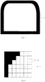
- Fig. 1 illustrates a schematic diagram of a structure of a display device.
- Fig. 2 illustrates a schematic diagram of a part of an array substrate of the display device as illustrated in Fig. 1 .
- an edge of a display region a of the display device is round-cornered macroscopically.
- pixels b in the display region a are generally rectangular, and since an arrangement of the pixels b at the edge is uneven, the edge of the display region a appears to be sawtoothed.
- the edge of the display region a will present a graininess and sawtooth feeling, thereby affecting the display effect of the display device.
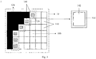
- the array substrate 1 may comprise a substrate 10.
- the substrate 10 has a display region 100 and a peripheral region 120 surrounding the display region 100.
- the peripheral region 120 may be disposed corresponding to a black matrix (not illustrated) on a color filter substrate (not illustrated).
- the display region 100 has a plurality of pixels 140 arranged in an array, and the pixels 140 may be disposed corresponding to color block (not illustrated) on the color filter substrate.
- the pixel 140 comprises a light transmission region 142 and a light shielding region 144.
- the pixels located outside the display region 100 constitute a plurality of edge pixels 160, i.e., pixels close to the peripheral region.
- the array substrate 1 may further comprise a light shielding block 20 that covers at least a part of the light transmission region 142 of the edge pixel 160 to shield light transmission.
- the light shielding block 20 covers at least a part of the light transmission region 142 of the edge pixel 160 of the array substrate 1, a light transmittance of the edge pixel 160 (i.e., a ratio of a difference between an area of the light transmission region and an area of the light shielding block to an area of the light transmission region) is reduced, and a brightness of the edge pixel 160 is decreased, thereby reducing the acuity of human eyes in capturing the edge of the display region having a non-rectangular shape, finally relieving the problem of graininess and sawtooth feeling at the edge of the display region, and improving the display effect.
- a light transmittance of the edge pixel 160 i.e., a ratio of a difference between an area of the light transmission region and an area of the light shielding block to an area of the light transmission region
- Fig. 3 illustrates only a part of the array substrate having the non-rectangular edge.
- the number of the pixels is not limited and can be set based on the actual need.
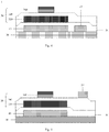
- Fig. 4 illustrates a cross-sectional diagram of an edge pixel of an array substrate 1 according to an embodiment of the present disclosure.
- the array substrate 1 may further comprise a thin film transistor 30 located on the substrate 10 and in the light shielding region 144.
- the thin film transistor 30 comprises an active layer 320, a gate dielectric layer 340, and a gate electrode 360 sequentially disposed on the substrate 10, i.e., the thin film transistor 30 is a top gate structure.
- a material of the active layer may comprise Low Temperature Poly-Silicon (LTPS).
- the array substrate 1 may further comprise a light shielding layer 40 located between the active layer 320 and the substrate 10.
- LTPS Low Temperature Poly-Silicon
- the light shielding layer 40 can prevent light rays from irradiating the active layer, and then avoid the performance of the thin film transistor 30 from being affected.
- the light shielding block 20 in the light transmitting region 142 of the edge pixel 160 may be disposed on a same layer as the light shielding layer 40.
- "disposed on a same layer” means being formed of a same film layer.
- the light shielding layer 40 and the light shielding block 20 thus may be made of a same material. In this case, the light shielding layer 40 and the light shielding block 20 can be simultaneously formed by the masking, exposing and etching processes at one time, thereby simplifying the process flow.
- an insulating layer 50 is disposed between the light shielding layer 40 and the active layer 320.
- the light transmittance of the edge pixel 160 can be reduced by disposing the light shielding block 20 in the light transmission region 142 of the edge pixel 160 of the array substrate 1, thereby relieving the problem of graininess and sawtooth feeling at the edge of the display region, and improving the display effect.
- the process flow can be simplified.
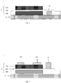
- Fig. 5 illustrates a cross-sectional diagram of an edge pixel of an array substrate 1 according to another embodiment of the present disclosure.
- the array substrate 1 may further comprise a thin film transistor 30 located on the substrate 10 and in the light shielding region 144.
- the thin film transistor 30 comprises an active layer 320, a gate dielectric layer 340, and a gate electrode 360 sequentially disposed on the substrate 10.
- the array substrate 1 further comprises a light shielding layer 40 disposed between the active layer 320 and the substrate 10, and an insulating layer 50 disposed between the light shielding layer 40 and the active layer 320.
- the light shielding block 20 in the light transmission region 142 of the edge pixel 160 may be disposed on a same layer as the gate electrode 360.
- the light shielding block 20 and the gate electrode 360 may be made of a same material.
- the light shielding block 20 and the gate electrode 360 can be simultaneously formed by the masking, exposing and etching processes at one time, thereby simplifying the process flow.
- Fig. 6 illustrates a cross-sectional diagram of an edge pixel of an array substrate 1 according to still another embodiment of the present disclosure.
- the array substrate 1 may further comprise a thin film transistor 32 located on the substrate 10 and in the light shielding region 144.
- the thin film transistor 32 comprises a gate electrode 360, a gate dielectric layer 340, and an active layer 320 sequentially disposed on the substrate 10, i.e., the thin film transistor 32 is a bottom gate structure.
- the light shielding block 20 in the light transmitting region 142 of the edge pixel 160 may be disposed on a same layer as the gate electrode 360.
- the light shielding block 20 and the gate electrode 360 may be made of a same material. In this case, the light shielding block 20 and the gate electrode 360 can be simultaneously formed by the masking, exposing and etching processes at one time, thereby simplifying the process flow.
- the light transmittance of the edge pixel 160 can be reduced by disposing the light shielding block 20 to cover at least a part of the light transmission region 142 of the edge pixel 160 of the array substrate 1, thereby relieving the problem of graininess and sawtooth feeling at the edge of the display region, and improving the display effect.
- the process flow can be simplified.
- Fig. 7 illustrates a cross-sectional diagram of an edge pixel of an array substrate 1 according to yet another embodiment of the present disclosure.
- the array substrate 1 may further comprise a thin film transistor 34 located on the substrate 10 and in the light shielding region 144.
- the thin film transistor 34 comprises a gate electrode 360, a gate dielectric layer 340 and an active layer 320 sequentially disposed on the substrate 10, i.e., the thin film transistor 34 is a bottom gate structure.
- the thin film transistor 34 may further comprise a source electrode 382/ drain electrode 384 disposed on the active layer 320.
- the light shielding block 20 in the light transmission region 142 of the edge pixel 160 may be disposed on a same layer as the source electrode 382/drain electrode 384.
- the light shielding block 20 and the source electrode 382/drain electrode 384 may be made of a same material. In this case, the light shielding block 20 and the source electrode 382/drain electrode 384 can be simultaneously formed by the masking, exposing and etching processes at one time, thereby simplifying the process flow.
- the light transmittance of the edge pixel 160 can be reduced by disposing the light shielding block 20 to cover at least a part of the light transmission region 142 of the edge pixel 160 of the array substrate 1, thereby relieving the problem of graininess and sawtooth feeling at the edge of the display region, and improving the display effect.
- the process flow can be simplified.
- Figs. 8A and 8B illustrate schematic diagrams of a structure of a pixel 140 according to an embodiment of the present disclosure.
- a pixel 140 and an edge pixel 160 each may comprise three sub-pixels 1402 located in a light transmission region 142.
- the sub-pixels 1402 may be red, green and blue sub-pixels, respectively, which may be disposed corresponding to respective color block (not illustrated) on the color film substrate.
- the light shielding block 20 may be disposed within the three sub-pixels 1402 to shield light transmission.
- the light shielding block 20 within each of the sub-pixels 1402 may have a same area, so that each of the sub-pixels 1402 in a same edge pixel 160 has a same light transmittance, thereby avoiding the problem that one of the sub-pixels 1402 is too bright and causing color difference.
- Figs. 9A and 9B illustrate schematic diagrams of a structure of an edge pixel 160 according to an embodiment of the present disclosure.
- the light shielding block 20 may comprise a first portion 202 and a second portion 204 that cover opposite ends of a light transmission region of an edge pixel 160, respectively. In this way, the edge pixel 160 can be covered finely to achieve a better display effect.
- the light shielding block 20 may further comprise a third portion 206 located between the first portion 202 and the second portion 204. In this way, the edge pixel 160 can be further covered finely to achieve a better display effect.
- an area of the light shielding block 20 of each of the edge pixels 160 may be set according to a desired shape of an edge of the display region 100.
- the area of each of the light shielding blocks may be different depending on the shape of the edge, it is necessary to separately design a mask for each of the light shielding blocks, which potentially increases the number of the masks.
- a ratio of the area of the light shielding block 20 of the edge pixel 160 to an area of the edge pixel 160 may be set as one of N values constituting an arithmetic progression, and specifically, 3 ⁇ N ⁇ 101.
- the arithmetic progression has a first item of 0 and a last item of 100%.
- N is equal to 9
- the arithmetic progression may be 0, 12.5%, 25%, 37.5%, 50%, 62.5%, 75%, 87.5%, 100%.
- an absolute value of a difference between one of the N values and a desired set value depending on the shape of the edge of the display region may be smaller than an absolute value of a difference between any other one of the N values and the desired set value.
- the ratio of the area of the light shielding block 20 of one of the edge pixels 160 to an area of the edge pixel 160 can be set as 62.5%, i.e., a value closest to 68% selected from the above arithmetic progression.
- N is equal to 3
- the arithmetic progression may be 0, 50%, 100%.
- N is equal to 4
- the arithmetic progression may be 0, 33.3%, 66.6%, 100%. It will be understood that the above N values may not constitute an arithmetic progression and can be set based on the actual needs.
- a method for manufacturing an array substrate described herein is provided.
- Fig. 10 illustrates a flowchart of a method for manufacturing an array substrate according to an embodiment of the present disclosure.
- the method for manufacturing the array substrate may comprise the following steps:
- the substrate has a display region and a peripheral region surrounding the display region.
- the display region has a plurality of pixels arranged in an array, and each of the pixels comprises a light transmission region and a light shielding region.
- the pixels located outside the display region constitute a plurality of edge pixels.
- the light shielding block may comprise a first portion and a second portion that cover opposite ends of a light transmission region of an edge pixel, respectively. In this way, the edge pixel can be covered finely to achieve a better display effect.
- the light shielding block may further comprise a third portion located between the first portion and the second portion. In this way, the edge pixel can be further covered finely to achieve a better display effect.
- an area of the light shielding block of each of the edge pixels may be set according to a desired shape of an edge of the display region.
- a ratio of the area of the light shielding block 20 of the edge pixel 160 to an area of the edge pixel 160 may be set as one of N values constituting an arithmetic progression, and specifically, 3 ⁇ N ⁇ 101.
- the arithmetic progression has a first item of 0 and a last item of 100%. This setting can reduce the number of the mask during manufacturing.
- N is equal to 9
- the arithmetic progression may be 0, 12.5%, 25%, 37.5%, 50%, 62.5%, 75%, 87.5%, 100%.
- N is equal to 3, and the arithmetic progression may be 0, 50%, 100%. In still another exemplary embodiment, N is equal to 4, and the arithmetic progression may be 0, 33.3%, 66.6%, 100%. It will be understood that the above N values may not constitute an arithmetic progression and can be set based on the actual needs.
- the light shielding block covers the light transmission region of the edge pixel, a light transmittance of the edge pixel is reduced, and a brightness of the edge pixel is decreased, thereby reducing the acuity of human eyes in capturing the edge of the display region having a non-rectangular shape, finally relieving the problem of graininess and sawtooth feeling at the edge of the display region, and improving the display effect.
- the method for manufacturing the array substrate may further comprise forming a thin film transistor on the substrate and in the light shielding region.
- the steps of forming the thin film transistor may comprise S201 to S206.
- the method for manufacturing the array substrate may further comprise forming a thin film transistor on the substrate and in the light shielding region.
- the steps of forming the thin film transistor may comprise S301 to S304.
- the method may further comprise forming a light shielding layer on the substrate and in the light shielding region, and forming a fourth insulating layer on the light shielding layer.
- the method for manufacturing the array substrate may further comprise forming a thin film transistor on the substrate and in the light shielding region.
- the steps of forming the thin film transistor may comprise S401 to S404.
- the method for manufacturing the array substrate may further comprise forming a thin film transistor on the substrate and in the light shielding region.
- the steps of forming the thin film transistor may comprise S501 to S506.
- a display device comprising the array substrate described in the aforementioned embodiments.
- Fig. 11 illustrates a schematic diagram of a display device according to an embodiment of the present disclosure.
- the display device 2 according to the present disclosure comprises the aforementioned array substrate 1.
- the light transmittance of the edge pixel can be reduced by disposing the light shielding block to cover at least a part of the light transmission region of the edge pixel of the array substrate of the display device, thereby relieving the problem of graininess and sawtooth feeling at the edge of the display region, and improving the display effect.
Landscapes
- Physics & Mathematics (AREA)
- Nonlinear Science (AREA)
- Mathematical Physics (AREA)
- Chemical & Material Sciences (AREA)
- Crystallography & Structural Chemistry (AREA)
- General Physics & Mathematics (AREA)
- Optics & Photonics (AREA)
- Engineering & Computer Science (AREA)
- Microelectronics & Electronic Packaging (AREA)
- Devices For Indicating Variable Information By Combining Individual Elements (AREA)
- Manufacturing & Machinery (AREA)
- Health & Medical Sciences (AREA)
- Electromagnetism (AREA)
- Toxicology (AREA)
- Liquid Crystal (AREA)
Applications Claiming Priority (2)
| Application Number | Priority Date | Filing Date | Title |
|---|---|---|---|
| CN201711313230.3A CN109920795A (zh) | 2017-12-12 | 2017-12-12 | 阵列基板及其制造方法、显示装置 |
| PCT/CN2018/113746 WO2019114456A1 (zh) | 2017-12-12 | 2018-11-02 | 阵列基板及其制造方法、显示装置 |
Publications (3)
| Publication Number | Publication Date |
|---|---|
| EP3731007A1 true EP3731007A1 (de) | 2020-10-28 |
| EP3731007A4 EP3731007A4 (de) | 2021-11-03 |
| EP3731007B1 EP3731007B1 (de) | 2025-06-04 |
Family
ID=66820747
Family Applications (1)
| Application Number | Title | Priority Date | Filing Date |
|---|---|---|---|
| EP18859964.1A Active EP3731007B1 (de) | 2017-12-12 | 2018-11-02 | Arraysubstrat und verfahren zur herstellung davon sowie anzeigevorrichtung |
Country Status (4)
| Country | Link |
|---|---|
| US (3) | US11404582B2 (de) |
| EP (1) | EP3731007B1 (de) |
| CN (1) | CN109920795A (de) |
| WO (1) | WO2019114456A1 (de) |
Cited By (1)
| Publication number | Priority date | Publication date | Assignee | Title |
|---|---|---|---|---|
| CN112701145A (zh) * | 2020-12-22 | 2021-04-23 | Oppo(重庆)智能科技有限公司 | 有机电致发光二极管显示面板及其制备方法、电子设备 |
Families Citing this family (3)
| Publication number | Priority date | Publication date | Assignee | Title |
|---|---|---|---|---|
| WO2021103014A1 (zh) * | 2019-11-29 | 2021-06-03 | 京东方科技集团股份有限公司 | 阵列基板、显示面板、拼接显示面板及显示驱动方法 |
| CN111352267A (zh) * | 2020-04-14 | 2020-06-30 | Tcl华星光电技术有限公司 | 一种显示面板 |
| KR102939861B1 (ko) * | 2020-10-22 | 2026-03-16 | 삼성디스플레이 주식회사 | 디스플레이 장치와, 이의 제조방법 |
Family Cites Families (26)
| Publication number | Priority date | Publication date | Assignee | Title |
|---|---|---|---|---|
| JP2002353424A (ja) * | 2001-03-23 | 2002-12-06 | Seiko Epson Corp | 基板装置の製造方法及び基板装置、電気光学装置の製造方法及び電気光学装置、並びに電子機器 |
| KR20070015805A (ko) | 2005-08-01 | 2007-02-06 | 삼성전자주식회사 | 색필터 표시판 및 이를 포함하는 액정표시장치 |
| JP5197206B2 (ja) * | 2008-07-25 | 2013-05-15 | 株式会社ジャパンディスプレイセントラル | 液晶表示装置 |
| JP5532481B2 (ja) * | 2009-05-13 | 2014-06-25 | Nltテクノロジー株式会社 | カラー画像表示方式、カラーフィルタ基板、カラー画素アレイ基板、画像表示装置及び電子機器 |
| CN102445790B (zh) * | 2010-10-06 | 2016-05-18 | 株式会社日本显示器 | 取向膜、取向膜形成用组合物和液晶显示装置 |
| KR101335526B1 (ko) | 2012-09-12 | 2013-12-02 | 엘지디스플레이 주식회사 | 입체영상 표시장치 |
| US9523896B2 (en) | 2014-04-03 | 2016-12-20 | Apple Inc. | Border masking structures for liquid crystal displays |
| CN104570457B (zh) | 2014-12-23 | 2017-11-24 | 上海天马微电子有限公司 | 一种彩色滤光基板及显示装置 |
| WO2016135929A1 (ja) | 2015-02-26 | 2016-09-01 | 堺ディスプレイプロダクト株式会社 | 液晶パネル及び液晶表示装置 |
| KR102354998B1 (ko) | 2015-03-18 | 2022-01-24 | 삼성디스플레이 주식회사 | 액정 표시 장치 |
| JP2017037131A (ja) * | 2015-08-07 | 2017-02-16 | 三菱電機株式会社 | アレイ基板とそのアレイ基板を用いた液晶表示装置 |
| CN105116480A (zh) * | 2015-10-15 | 2015-12-02 | 京东方科技集团股份有限公司 | 一种彩膜基板、显示面板及显示装置 |
| CN205334901U (zh) * | 2016-01-25 | 2016-06-22 | 成都京东方光电科技有限公司 | 异形显示面板及显示装置 |
| CN105511152A (zh) * | 2016-02-02 | 2016-04-20 | 京东方科技集团股份有限公司 | 显示基板、显示面板和显示装置 |
| JP2017181820A (ja) | 2016-03-30 | 2017-10-05 | パナソニック液晶ディスプレイ株式会社 | 曲面ディスプレイを備えた車載デバイス |
| CN106292108B (zh) * | 2016-09-08 | 2019-03-29 | 京东方科技集团股份有限公司 | 一种阵列基板及显示面板 |
| TWI623795B (zh) | 2017-03-17 | 2018-05-11 | 友達光電股份有限公司 | 遮光圖案 |
| CN107357066B (zh) | 2017-06-30 | 2020-04-03 | 厦门天马微电子有限公司 | 异形显示面板和显示装置 |
| CN107167957B (zh) | 2017-07-04 | 2019-11-26 | 厦门天马微电子有限公司 | 异形显示面板及显示装置 |
| CN107255883A (zh) * | 2017-08-01 | 2017-10-17 | 京东方科技集团股份有限公司 | 一种显示基板及显示装置 |
| CN107390422B (zh) * | 2017-08-22 | 2019-12-03 | 厦门天马微电子有限公司 | 一种异形显示面板和显示装置 |
| CN107390444B (zh) * | 2017-09-06 | 2024-03-29 | 京东方科技集团股份有限公司 | 一种阵列基板及其制作方法和显示装置 |
| CN107422516B (zh) | 2017-09-19 | 2020-01-21 | 厦门天马微电子有限公司 | 异形显示面板和显示装置 |
| CN107742499B (zh) | 2017-11-30 | 2021-02-19 | 武汉天马微电子有限公司 | 一种异形显示面板及显示装置 |
| CN107861288B (zh) | 2017-12-14 | 2020-12-29 | 京东方科技集团股份有限公司 | 显示面板和显示装置 |
| CN108364568B (zh) | 2018-03-19 | 2020-05-12 | 京东方科技集团股份有限公司 | 一种显示面板、显示装置及彩膜基板 |
-
2017
- 2017-12-12 CN CN201711313230.3A patent/CN109920795A/zh active Pending
-
2018
- 2018-11-02 US US16/343,485 patent/US11404582B2/en active Active
- 2018-11-02 WO PCT/CN2018/113746 patent/WO2019114456A1/zh not_active Ceased
- 2018-11-02 EP EP18859964.1A patent/EP3731007B1/de active Active
-
2022
- 2022-06-21 US US17/845,568 patent/US11728435B2/en active Active
-
2023
- 2023-06-28 US US18/343,279 patent/US12002887B2/en active Active
Cited By (1)
| Publication number | Priority date | Publication date | Assignee | Title |
|---|---|---|---|---|
| CN112701145A (zh) * | 2020-12-22 | 2021-04-23 | Oppo(重庆)智能科技有限公司 | 有机电致发光二极管显示面板及其制备方法、电子设备 |
Also Published As
| Publication number | Publication date |
|---|---|
| US20230343874A1 (en) | 2023-10-26 |
| EP3731007A4 (de) | 2021-11-03 |
| US12002887B2 (en) | 2024-06-04 |
| US20210336065A1 (en) | 2021-10-28 |
| US11404582B2 (en) | 2022-08-02 |
| EP3731007B1 (de) | 2025-06-04 |
| US11728435B2 (en) | 2023-08-15 |
| WO2019114456A1 (zh) | 2019-06-20 |
| CN109920795A (zh) | 2019-06-21 |
| US20220320345A1 (en) | 2022-10-06 |
Similar Documents
| Publication | Publication Date | Title |
|---|---|---|
| US12002887B2 (en) | Array substrate and method for manufacturing the same, and display device | |
| US20210202621A1 (en) | Display panel and display device | |
| US20170108630A1 (en) | Color filter substrate, display panel and display device | |
| EP3076437A1 (de) | Dünnschichttransistor und herstellungsverfahren dafür, anzeigesubstrat und anzeigevorrichtung | |
| US20140092497A1 (en) | Color Filter and Related Manufacturing Method Thereof | |
| US20150179668A1 (en) | Thin film transistor array substrate, method for fabricating the same and display | |
| CN108376523B (zh) | 一种显示面板和显示装置 | |
| CN108681137B (zh) | 一种显示基板及其制作方法、显示面板、显示装置 | |
| EP3534208A1 (de) | Arraysubstrat und herstellungsverfahren dafür sowie flüssigkristallanzeigetafel | |
| US10365523B2 (en) | Display panel and manufacturing method based on BOA technology | |
| US20170139247A1 (en) | Thin Film Transistor Array Substrate, Manufacturing for the Same, and Liquid Crystal Display Panel Having the Same | |
| EP3349061A1 (de) | Arraysubstrat, herstellungsverfahren dafür, anzeigetafel und anzeigevorrichtung | |
| KR20170096007A (ko) | 어레이 기판, 디스플레이 패널, 및 어레이 기판의 제조 방법 | |
| US11402700B2 (en) | Display panel having pixel units on transition area | |
| EP3767379A1 (de) | Anzeigesubstrat, herstellungsverfahren, anzeigetafel und anzeigevorrichtung | |
| CN113066846B (zh) | 显示面板及电子设备 | |
| CN109507817A (zh) | 显示装置、阵列基板及其工艺方法 | |
| US9791755B2 (en) | Color filter-on-array substrate, display device, and method for manufacturing the color filter-on-array substrate | |
| WO2021012360A1 (zh) | 显示面板及制作方法、显示装置 | |
| US20150372013A1 (en) | Array substrate, manufacturing method thereof, and display device | |
| US9847427B2 (en) | Array substrate, method for fabricating the same, and display device | |
| CN109507827B (zh) | 显示面板制作方法、显示面板制作装置和显示面板 | |
| EP3088952B1 (de) | Maskengruppe, pixeleinheit und herstellungsverfahren dafür, arraysubstrat und anzeigevorrichtung | |
| CN112904631A (zh) | 一种阵列基板及其制备方法、显示面板及显示装置 | |
| CN108196411B (zh) | 液晶显示面板及其显示装置 |
Legal Events
| Date | Code | Title | Description |
|---|---|---|---|
| STAA | Information on the status of an ep patent application or granted ep patent |
Free format text: STATUS: UNKNOWN |
|
| STAA | Information on the status of an ep patent application or granted ep patent |
Free format text: STATUS: THE INTERNATIONAL PUBLICATION HAS BEEN MADE |
|
| PUAI | Public reference made under article 153(3) epc to a published international application that has entered the european phase |
Free format text: ORIGINAL CODE: 0009012 |
|
| STAA | Information on the status of an ep patent application or granted ep patent |
Free format text: STATUS: REQUEST FOR EXAMINATION WAS MADE |
|
| 17P | Request for examination filed |
Effective date: 20190403 |
|
| AK | Designated contracting states |
Kind code of ref document: A1 Designated state(s): AL AT BE BG CH CY CZ DE DK EE ES FI FR GB GR HR HU IE IS IT LI LT LU LV MC MK MT NL NO PL PT RO RS SE SI SK SM TR |
|
| AX | Request for extension of the european patent |
Extension state: BA ME |
|
| DAV | Request for validation of the european patent (deleted) | ||
| DAX | Request for extension of the european patent (deleted) | ||
| REG | Reference to a national code |
Ref legal event code: R079 Free format text: PREVIOUS MAIN CLASS: G02F0001133500 Ref country code: DE Ref legal event code: R079 Ref document number: 602018082465 Country of ref document: DE Free format text: PREVIOUS MAIN CLASS: G02F0001133500 Ipc: G02F0001133300 |
|
| A4 | Supplementary search report drawn up and despatched |
Effective date: 20211006 |
|
| RIC1 | Information provided on ipc code assigned before grant |
Ipc: G02F 1/1362 20060101ALI20210930BHEP Ipc: G02F 1/1333 20060101AFI20210930BHEP |
|
| STAA | Information on the status of an ep patent application or granted ep patent |
Free format text: STATUS: EXAMINATION IS IN PROGRESS |
|
| 17Q | First examination report despatched |
Effective date: 20230418 |
|
| GRAP | Despatch of communication of intention to grant a patent |
Free format text: ORIGINAL CODE: EPIDOSNIGR1 |
|
| STAA | Information on the status of an ep patent application or granted ep patent |
Free format text: STATUS: GRANT OF PATENT IS INTENDED |
|
| INTG | Intention to grant announced |
Effective date: 20250227 |
|
| GRAS | Grant fee paid |
Free format text: ORIGINAL CODE: EPIDOSNIGR3 |
|
| GRAA | (expected) grant |
Free format text: ORIGINAL CODE: 0009210 |
|
| STAA | Information on the status of an ep patent application or granted ep patent |
Free format text: STATUS: THE PATENT HAS BEEN GRANTED |
|
| AK | Designated contracting states |
Kind code of ref document: B1 Designated state(s): AL AT BE BG CH CY CZ DE DK EE ES FI FR GB GR HR HU IE IS IT LI LT LU LV MC MK MT NL NO PL PT RO RS SE SI SK SM TR |
|
| REG | Reference to a national code |
Ref country code: GB Ref legal event code: FG4D |
|
| REG | Reference to a national code |
Ref country code: CH Ref legal event code: EP |
|
| REG | Reference to a national code |
Ref country code: DE Ref legal event code: R096 Ref document number: 602018082465 Country of ref document: DE |
|
| REG | Reference to a national code |
Ref country code: IE Ref legal event code: FG4D |
|
| REG | Reference to a national code |
Ref country code: NL Ref legal event code: MP Effective date: 20250604 |
|
| PG25 | Lapsed in a contracting state [announced via postgrant information from national office to epo] |
Ref country code: FI Free format text: LAPSE BECAUSE OF FAILURE TO SUBMIT A TRANSLATION OF THE DESCRIPTION OR TO PAY THE FEE WITHIN THE PRESCRIBED TIME-LIMIT Effective date: 20250604 Ref country code: ES Free format text: LAPSE BECAUSE OF FAILURE TO SUBMIT A TRANSLATION OF THE DESCRIPTION OR TO PAY THE FEE WITHIN THE PRESCRIBED TIME-LIMIT Effective date: 20250604 |
|
| REG | Reference to a national code |
Ref country code: LT Ref legal event code: MG9D |
|
| PG25 | Lapsed in a contracting state [announced via postgrant information from national office to epo] |
Ref country code: GR Free format text: LAPSE BECAUSE OF FAILURE TO SUBMIT A TRANSLATION OF THE DESCRIPTION OR TO PAY THE FEE WITHIN THE PRESCRIBED TIME-LIMIT Effective date: 20250905 Ref country code: NO Free format text: LAPSE BECAUSE OF FAILURE TO SUBMIT A TRANSLATION OF THE DESCRIPTION OR TO PAY THE FEE WITHIN THE PRESCRIBED TIME-LIMIT Effective date: 20250904 |
|
| PG25 | Lapsed in a contracting state [announced via postgrant information from national office to epo] |
Ref country code: PL Free format text: LAPSE BECAUSE OF FAILURE TO SUBMIT A TRANSLATION OF THE DESCRIPTION OR TO PAY THE FEE WITHIN THE PRESCRIBED TIME-LIMIT Effective date: 20250604 |
|
| PG25 | Lapsed in a contracting state [announced via postgrant information from national office to epo] |
Ref country code: BG Free format text: LAPSE BECAUSE OF FAILURE TO SUBMIT A TRANSLATION OF THE DESCRIPTION OR TO PAY THE FEE WITHIN THE PRESCRIBED TIME-LIMIT Effective date: 20250604 |
|
| PG25 | Lapsed in a contracting state [announced via postgrant information from national office to epo] |
Ref country code: HR Free format text: LAPSE BECAUSE OF FAILURE TO SUBMIT A TRANSLATION OF THE DESCRIPTION OR TO PAY THE FEE WITHIN THE PRESCRIBED TIME-LIMIT Effective date: 20250604 |
|
| PG25 | Lapsed in a contracting state [announced via postgrant information from national office to epo] |
Ref country code: RS Free format text: LAPSE BECAUSE OF FAILURE TO SUBMIT A TRANSLATION OF THE DESCRIPTION OR TO PAY THE FEE WITHIN THE PRESCRIBED TIME-LIMIT Effective date: 20250904 |
|
| PG25 | Lapsed in a contracting state [announced via postgrant information from national office to epo] |
Ref country code: LV Free format text: LAPSE BECAUSE OF FAILURE TO SUBMIT A TRANSLATION OF THE DESCRIPTION OR TO PAY THE FEE WITHIN THE PRESCRIBED TIME-LIMIT Effective date: 20250604 |
|
| PG25 | Lapsed in a contracting state [announced via postgrant information from national office to epo] |
Ref country code: NL Free format text: LAPSE BECAUSE OF FAILURE TO SUBMIT A TRANSLATION OF THE DESCRIPTION OR TO PAY THE FEE WITHIN THE PRESCRIBED TIME-LIMIT Effective date: 20250604 |
|
| PG25 | Lapsed in a contracting state [announced via postgrant information from national office to epo] |
Ref country code: PT Free format text: LAPSE BECAUSE OF FAILURE TO SUBMIT A TRANSLATION OF THE DESCRIPTION OR TO PAY THE FEE WITHIN THE PRESCRIBED TIME-LIMIT Effective date: 20251006 |
|
| REG | Reference to a national code |
Ref country code: AT Ref legal event code: MK05 Ref document number: 1800879 Country of ref document: AT Kind code of ref document: T Effective date: 20250604 |
|
| PG25 | Lapsed in a contracting state [announced via postgrant information from national office to epo] |
Ref country code: IS Free format text: LAPSE BECAUSE OF FAILURE TO SUBMIT A TRANSLATION OF THE DESCRIPTION OR TO PAY THE FEE WITHIN THE PRESCRIBED TIME-LIMIT Effective date: 20251004 |
|
| PGFP | Annual fee paid to national office [announced via postgrant information from national office to epo] |
Ref country code: DE Payment date: 20251119 Year of fee payment: 8 |
|
| PGFP | Annual fee paid to national office [announced via postgrant information from national office to epo] |
Ref country code: GB Payment date: 20251121 Year of fee payment: 8 |
|
| PG25 | Lapsed in a contracting state [announced via postgrant information from national office to epo] |
Ref country code: SM Free format text: LAPSE BECAUSE OF FAILURE TO SUBMIT A TRANSLATION OF THE DESCRIPTION OR TO PAY THE FEE WITHIN THE PRESCRIBED TIME-LIMIT Effective date: 20250604 Ref country code: AT Free format text: LAPSE BECAUSE OF FAILURE TO SUBMIT A TRANSLATION OF THE DESCRIPTION OR TO PAY THE FEE WITHIN THE PRESCRIBED TIME-LIMIT Effective date: 20250604 |
|
| PG25 | Lapsed in a contracting state [announced via postgrant information from national office to epo] |
Ref country code: CZ Free format text: LAPSE BECAUSE OF FAILURE TO SUBMIT A TRANSLATION OF THE DESCRIPTION OR TO PAY THE FEE WITHIN THE PRESCRIBED TIME-LIMIT Effective date: 20250604 |
|
| PG25 | Lapsed in a contracting state [announced via postgrant information from national office to epo] |
Ref country code: EE Free format text: LAPSE BECAUSE OF FAILURE TO SUBMIT A TRANSLATION OF THE DESCRIPTION OR TO PAY THE FEE WITHIN THE PRESCRIBED TIME-LIMIT Effective date: 20250604 |
|
| PG25 | Lapsed in a contracting state [announced via postgrant information from national office to epo] |
Ref country code: SK Free format text: LAPSE BECAUSE OF FAILURE TO SUBMIT A TRANSLATION OF THE DESCRIPTION OR TO PAY THE FEE WITHIN THE PRESCRIBED TIME-LIMIT Effective date: 20250604 Ref country code: RO Free format text: LAPSE BECAUSE OF FAILURE TO SUBMIT A TRANSLATION OF THE DESCRIPTION OR TO PAY THE FEE WITHIN THE PRESCRIBED TIME-LIMIT Effective date: 20250604 |
|
| PG25 | Lapsed in a contracting state [announced via postgrant information from national office to epo] |
Ref country code: IT Free format text: LAPSE BECAUSE OF FAILURE TO SUBMIT A TRANSLATION OF THE DESCRIPTION OR TO PAY THE FEE WITHIN THE PRESCRIBED TIME-LIMIT Effective date: 20250604 |
|
| REG | Reference to a national code |
Ref country code: DE Ref legal event code: R097 Ref document number: 602018082465 Country of ref document: DE |
|
| PLBE | No opposition filed within time limit |
Free format text: ORIGINAL CODE: 0009261 |
|
| STAA | Information on the status of an ep patent application or granted ep patent |
Free format text: STATUS: NO OPPOSITION FILED WITHIN TIME LIMIT |
|
| PG25 | Lapsed in a contracting state [announced via postgrant information from national office to epo] |
Ref country code: DK Free format text: LAPSE BECAUSE OF FAILURE TO SUBMIT A TRANSLATION OF THE DESCRIPTION OR TO PAY THE FEE WITHIN THE PRESCRIBED TIME-LIMIT Effective date: 20250604 |
|
| REG | Reference to a national code |
Ref country code: CH Ref legal event code: L10 Free format text: ST27 STATUS EVENT CODE: U-0-0-L10-L00 (AS PROVIDED BY THE NATIONAL OFFICE) Effective date: 20260416 |