EP3706255B1 - Leiterplattendirektverbinder mit zweireihiger anschlussstruktur - Google Patents
Leiterplattendirektverbinder mit zweireihiger anschlussstruktur Download PDFInfo
- Publication number
- EP3706255B1 EP3706255B1 EP19818817.9A EP19818817A EP3706255B1 EP 3706255 B1 EP3706255 B1 EP 3706255B1 EP 19818817 A EP19818817 A EP 19818817A EP 3706255 B1 EP3706255 B1 EP 3706255B1
- Authority
- EP
- European Patent Office
- Prior art keywords
- connector
- circuit board
- connector housing
- upper plate
- terminal members
- Prior art date
- Legal status (The legal status is an assumption and is not a legal conclusion. Google has not performed a legal analysis and makes no representation as to the accuracy of the status listed.)
- Active
Links
Images


Classifications
-
- H—ELECTRICITY
- H01—ELECTRIC ELEMENTS
- H01R—ELECTRICALLY-CONDUCTIVE CONNECTIONS; STRUCTURAL ASSOCIATIONS OF A PLURALITY OF MUTUALLY-INSULATED ELECTRICAL CONNECTING ELEMENTS; COUPLING DEVICES; CURRENT COLLECTORS
- H01R12/00—Structural associations of a plurality of mutually-insulated electrical connecting elements, specially adapted for printed circuits, e.g. printed circuit boards [PCB], flat or ribbon cables, or like generally planar structures, e.g. terminal strips, terminal blocks; Coupling devices specially adapted for printed circuits, flat or ribbon cables, or like generally planar structures; Terminals specially adapted for contact with, or insertion into, printed circuits, flat or ribbon cables, or like generally planar structures
- H01R12/70—Coupling devices
- H01R12/77—Coupling devices for flexible printed circuits, flat or ribbon cables or like structures
- H01R12/771—Details
- H01R12/774—Retainers
-
- H—ELECTRICITY
- H01—ELECTRIC ELEMENTS
- H01R—ELECTRICALLY-CONDUCTIVE CONNECTIONS; STRUCTURAL ASSOCIATIONS OF A PLURALITY OF MUTUALLY-INSULATED ELECTRICAL CONNECTING ELEMENTS; COUPLING DEVICES; CURRENT COLLECTORS
- H01R12/00—Structural associations of a plurality of mutually-insulated electrical connecting elements, specially adapted for printed circuits, e.g. printed circuit boards [PCB], flat or ribbon cables, or like generally planar structures, e.g. terminal strips, terminal blocks; Coupling devices specially adapted for printed circuits, flat or ribbon cables, or like generally planar structures; Terminals specially adapted for contact with, or insertion into, printed circuits, flat or ribbon cables, or like generally planar structures
- H01R12/70—Coupling devices
- H01R12/71—Coupling devices for rigid printing circuits or like structures
- H01R12/72—Coupling devices for rigid printing circuits or like structures coupling with the edge of the rigid printed circuits or like structures
- H01R12/721—Coupling devices for rigid printing circuits or like structures coupling with the edge of the rigid printed circuits or like structures cooperating directly with the edge of the rigid printed circuits
-
- H—ELECTRICITY
- H01—ELECTRIC ELEMENTS
- H01R—ELECTRICALLY-CONDUCTIVE CONNECTIONS; STRUCTURAL ASSOCIATIONS OF A PLURALITY OF MUTUALLY-INSULATED ELECTRICAL CONNECTING ELEMENTS; COUPLING DEVICES; CURRENT COLLECTORS
- H01R12/00—Structural associations of a plurality of mutually-insulated electrical connecting elements, specially adapted for printed circuits, e.g. printed circuit boards [PCB], flat or ribbon cables, or like generally planar structures, e.g. terminal strips, terminal blocks; Coupling devices specially adapted for printed circuits, flat or ribbon cables, or like generally planar structures; Terminals specially adapted for contact with, or insertion into, printed circuits, flat or ribbon cables, or like generally planar structures
- H01R12/50—Fixed connections
- H01R12/51—Fixed connections for rigid printed circuits or like structures
- H01R12/55—Fixed connections for rigid printed circuits or like structures characterised by the terminals
- H01R12/58—Fixed connections for rigid printed circuits or like structures characterised by the terminals terminals for insertion into holes
-
- H—ELECTRICITY
- H01—ELECTRIC ELEMENTS
- H01R—ELECTRICALLY-CONDUCTIVE CONNECTIONS; STRUCTURAL ASSOCIATIONS OF A PLURALITY OF MUTUALLY-INSULATED ELECTRICAL CONNECTING ELEMENTS; COUPLING DEVICES; CURRENT COLLECTORS
- H01R12/00—Structural associations of a plurality of mutually-insulated electrical connecting elements, specially adapted for printed circuits, e.g. printed circuit boards [PCB], flat or ribbon cables, or like generally planar structures, e.g. terminal strips, terminal blocks; Coupling devices specially adapted for printed circuits, flat or ribbon cables, or like generally planar structures; Terminals specially adapted for contact with, or insertion into, printed circuits, flat or ribbon cables, or like generally planar structures
- H01R12/70—Coupling devices
- H01R12/7005—Guiding, mounting, polarizing or locking means; Extractors
-
- H—ELECTRICITY
- H01—ELECTRIC ELEMENTS
- H01R—ELECTRICALLY-CONDUCTIVE CONNECTIONS; STRUCTURAL ASSOCIATIONS OF A PLURALITY OF MUTUALLY-INSULATED ELECTRICAL CONNECTING ELEMENTS; COUPLING DEVICES; CURRENT COLLECTORS
- H01R12/00—Structural associations of a plurality of mutually-insulated electrical connecting elements, specially adapted for printed circuits, e.g. printed circuit boards [PCB], flat or ribbon cables, or like generally planar structures, e.g. terminal strips, terminal blocks; Coupling devices specially adapted for printed circuits, flat or ribbon cables, or like generally planar structures; Terminals specially adapted for contact with, or insertion into, printed circuits, flat or ribbon cables, or like generally planar structures
- H01R12/70—Coupling devices
- H01R12/71—Coupling devices for rigid printing circuits or like structures
- H01R12/712—Coupling devices for rigid printing circuits or like structures co-operating with the surface of the printed circuit or with a coupling device exclusively provided on the surface of the printed circuit
- H01R12/716—Coupling device provided on the PCB
-
- H—ELECTRICITY
- H01—ELECTRIC ELEMENTS
- H01R—ELECTRICALLY-CONDUCTIVE CONNECTIONS; STRUCTURAL ASSOCIATIONS OF A PLURALITY OF MUTUALLY-INSULATED ELECTRICAL CONNECTING ELEMENTS; COUPLING DEVICES; CURRENT COLLECTORS
- H01R12/00—Structural associations of a plurality of mutually-insulated electrical connecting elements, specially adapted for printed circuits, e.g. printed circuit boards [PCB], flat or ribbon cables, or like generally planar structures, e.g. terminal strips, terminal blocks; Coupling devices specially adapted for printed circuits, flat or ribbon cables, or like generally planar structures; Terminals specially adapted for contact with, or insertion into, printed circuits, flat or ribbon cables, or like generally planar structures
- H01R12/70—Coupling devices
- H01R12/82—Coupling devices connected with low or zero insertion force
- H01R12/85—Coupling devices connected with low or zero insertion force contact pressure producing means, contacts activated after insertion of printed circuits or like structures
- H01R12/89—Coupling devices connected with low or zero insertion force contact pressure producing means, contacts activated after insertion of printed circuits or like structures acting manually by moving connector housing parts linearly, e.g. slider
-
- H—ELECTRICITY
- H01—ELECTRIC ELEMENTS
- H01R—ELECTRICALLY-CONDUCTIVE CONNECTIONS; STRUCTURAL ASSOCIATIONS OF A PLURALITY OF MUTUALLY-INSULATED ELECTRICAL CONNECTING ELEMENTS; COUPLING DEVICES; CURRENT COLLECTORS
- H01R13/00—Details of coupling devices of the kinds covered by groups H01R12/70 or H01R24/00 - H01R33/00
- H01R13/02—Contact members
- H01R13/22—Contacts for co-operating by abutting
- H01R13/24—Contacts for co-operating by abutting resilient; resiliently-mounted
- H01R13/2435—Contacts for co-operating by abutting resilient; resiliently-mounted with opposite contact points, e.g. C beam
-
- H—ELECTRICITY
- H01—ELECTRIC ELEMENTS
- H01R—ELECTRICALLY-CONDUCTIVE CONNECTIONS; STRUCTURAL ASSOCIATIONS OF A PLURALITY OF MUTUALLY-INSULATED ELECTRICAL CONNECTING ELEMENTS; COUPLING DEVICES; CURRENT COLLECTORS
- H01R13/00—Details of coupling devices of the kinds covered by groups H01R12/70 or H01R24/00 - H01R33/00
- H01R13/02—Contact members
- H01R13/22—Contacts for co-operating by abutting
- H01R13/24—Contacts for co-operating by abutting resilient; resiliently-mounted
- H01R13/2457—Contacts for co-operating by abutting resilient; resiliently-mounted consisting of at least two resilient arms contacting the same counterpart
-
- H—ELECTRICITY
- H01—ELECTRIC ELEMENTS
- H01R—ELECTRICALLY-CONDUCTIVE CONNECTIONS; STRUCTURAL ASSOCIATIONS OF A PLURALITY OF MUTUALLY-INSULATED ELECTRICAL CONNECTING ELEMENTS; COUPLING DEVICES; CURRENT COLLECTORS
- H01R13/00—Details of coupling devices of the kinds covered by groups H01R12/70 or H01R24/00 - H01R33/00
- H01R13/02—Contact members
- H01R13/26—Pin or blade contacts for sliding co-operation on one side only
-
- H—ELECTRICITY
- H01—ELECTRIC ELEMENTS
- H01R—ELECTRICALLY-CONDUCTIVE CONNECTIONS; STRUCTURAL ASSOCIATIONS OF A PLURALITY OF MUTUALLY-INSULATED ELECTRICAL CONNECTING ELEMENTS; COUPLING DEVICES; CURRENT COLLECTORS
- H01R13/00—Details of coupling devices of the kinds covered by groups H01R12/70 or H01R24/00 - H01R33/00
- H01R13/40—Securing contact members in or to a base or case; Insulating of contact members
- H01R13/42—Securing in a demountable manner
- H01R13/436—Securing a plurality of contact members by one locking piece or operation
- H01R13/4361—Insertion of locking piece perpendicular to direction of contact insertion
-
- H—ELECTRICITY
- H01—ELECTRIC ELEMENTS
- H01R—ELECTRICALLY-CONDUCTIVE CONNECTIONS; STRUCTURAL ASSOCIATIONS OF A PLURALITY OF MUTUALLY-INSULATED ELECTRICAL CONNECTING ELEMENTS; COUPLING DEVICES; CURRENT COLLECTORS
- H01R13/00—Details of coupling devices of the kinds covered by groups H01R12/70 or H01R24/00 - H01R33/00
- H01R13/46—Bases; Cases
- H01R13/502—Bases; Cases composed of different pieces
-
- H—ELECTRICITY
- H01—ELECTRIC ELEMENTS
- H01R—ELECTRICALLY-CONDUCTIVE CONNECTIONS; STRUCTURAL ASSOCIATIONS OF A PLURALITY OF MUTUALLY-INSULATED ELECTRICAL CONNECTING ELEMENTS; COUPLING DEVICES; CURRENT COLLECTORS
- H01R13/00—Details of coupling devices of the kinds covered by groups H01R12/70 or H01R24/00 - H01R33/00
- H01R13/62—Means for facilitating engagement or disengagement of coupling parts or for holding them in engagement
- H01R13/627—Snap or like fastening
- H01R13/6271—Latching means integral with the housing
- H01R13/6272—Latching means integral with the housing comprising a single latching arm
-
- H—ELECTRICITY
- H01—ELECTRIC ELEMENTS
- H01R—ELECTRICALLY-CONDUCTIVE CONNECTIONS; STRUCTURAL ASSOCIATIONS OF A PLURALITY OF MUTUALLY-INSULATED ELECTRICAL CONNECTING ELEMENTS; COUPLING DEVICES; CURRENT COLLECTORS
- H01R13/00—Details of coupling devices of the kinds covered by groups H01R12/70 or H01R24/00 - H01R33/00
- H01R13/62—Means for facilitating engagement or disengagement of coupling parts or for holding them in engagement
- H01R13/629—Additional means for facilitating engagement or disengagement of coupling parts, e.g. aligning or guiding means, levers, gas pressure electrical locking indicators, manufacturing tolerances
-
- H—ELECTRICITY
- H01—ELECTRIC ELEMENTS
- H01R—ELECTRICALLY-CONDUCTIVE CONNECTIONS; STRUCTURAL ASSOCIATIONS OF A PLURALITY OF MUTUALLY-INSULATED ELECTRICAL CONNECTING ELEMENTS; COUPLING DEVICES; CURRENT COLLECTORS
- H01R13/00—Details of coupling devices of the kinds covered by groups H01R12/70 or H01R24/00 - H01R33/00
- H01R13/62—Means for facilitating engagement or disengagement of coupling parts or for holding them in engagement
- H01R13/629—Additional means for facilitating engagement or disengagement of coupling parts, e.g. aligning or guiding means, levers, gas pressure electrical locking indicators, manufacturing tolerances
- H01R13/631—Additional means for facilitating engagement or disengagement of coupling parts, e.g. aligning or guiding means, levers, gas pressure electrical locking indicators, manufacturing tolerances for engagement only
Definitions
- the present disclosure relates to a connector, and more particularly, to a connector that may be directly coupled to a PCB substrate without a complementary connector and include a large number of terminals with a compact size.
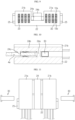
- a conventional connector generally includes a female connector 3 and a male connector 2 in a pair.
- the female connector 3 has a plurality of pins corresponding to a contact
- the male connector 2 has a plurality of plug terminals that come into contact with the plurality of pins.
- the male connector 2 is mounted to a circuit board 1by means of SMT (Surface Mounter Technology), and the female connector 3 is complementarily coupled with the male connector 2.
- FIG. 1 shows an 8-pin connector having 8 terminal pins.
- the right and left width of the connector is increased more than twice compared to the 8-pin connector.
- the area of the circuit board on which the connector is mounted increases accordingly, so that the space utilization of the device using the connector and the circuit board may deteriorate.
- the present disclosure is directed to providing a connector, which may be directly mounted on a circuit board to reduce component costs of the connector and process costs for the existing Surface Mounting Technology (SMT) process.
- SMT Surface Mounting Technology
- the present disclosure is directed to providing a connector, which may be stably fixed to the circuit board even against external impact and vibration to prevent separation or connection fault of the connector and also allow a plurality of components of the connector to be conveniently assembled and disassembled.
- the present disclosure is directed to providing a connector, which may be implemented with a compact size in comparison to the existing connector.
- a PCB direct connector as defined by the independent claim 1. Preferred embodiments are defined in the appended dependent claims.
- a PCB direct connector which is directly mounted to a circuit board, the PCB direct connector comprising: terminal members arranged in two rows to respectively contact upper conductive patterns and lower conductive patterns provided to an upper surface and a lower surface of the circuit board; and a connector housing configured to accommodate the terminal members therein and allow a connector connection portion formed at one side of an end of the circuit board to be fitted into and released from the connector housing.
- the connector housing includes an upper plate and a lower plate, and front portions of the upper plate and the lower plate may be spaced apart from each other as much as at least a thickness of the circuit board so that the connector connection portion is inserted therebetween to a predetermined depth, and rear portions of the upper plate and the lower plate may be connected to each other to form a single body.
- the rear portions of the upper plate and the lower plate may have insert holes into which the terminal members are inserted in two rows such that two terminal members are inserted into each insert hole.
- the terminal members may include a terminal body having a horizontal body formed to extend toward a portion where a signal transmission cable is connected and a pair of vertical bodies formed to extend in the same direction orthogonal to the horizontal body with a predetermined gap therebetween, the terminal body being interposed in the insert hole; and a contact portion formed to extend from the terminal body so that at least a part of the contact portion has a curved shape to elastically contact the upper surface or the lower surface of the circuit board, the contact portion being interposed at a front portion of the connector housing.
- the terminal members may include first-row terminal members and second-row terminal members symmetrically arranged inside the connector housing, the connector housing may have a side hole formed in at least one side surface thereof in a direction intersecting with the insert holes so as to communicate with a space surrounded by terminal bodies of the first-row terminal members and terminal bodies of the second-row terminal members, and the PCB direct connector may further comprise a retainer inserted into the side hole to integrally fix the first-row terminal members and the second-row terminal members.
- the connector housing may have a plurality of grooves formed by depressing a surface around the side hole, and the retainer may include a stopper configured to engage with a part of the plurality of grooves.
- the upper plate of the connector housing is divided into to two parts including a first upper plate and a second upper plate, and a latch is provided between the first upper plate and the second upper plate, and the latch has a hook provided at one end thereof so as to be hooked to a fastening hole provided in the circuit board in advance.
- the latch may include a shaft configured to protrude orthogonal to an upper surface of the lower plate located between the first upper plate and the second upper plate; and a latch plate configured to have the hook and extend parallel to the upper plate, the latch plate being connected to the shaft to make a seesawing operation based on the shaft.
- Both side surfaces of the connector housing has substrate holding ribs configured to be fitted into ends of the circuit board at both sides based on the connector connection portion.
- the substrate holding ribs are provided to the rear portions of the upper plate and the lower plate, and the substrate holding ribs have inlets formed with a width greater than the thickness of the circuit board, and the width of the inlets gradually decrease in a direction along which an end of the circuit board is inserted.
- the PCB direct connector may further comprise an insert limit plate provided at a border of a front portion and a rear portion of the connector housing to extend along a left and right width of the connector housing and form a predetermined wall for partially blocking outlets of the insert holes.
- the retainer may further include a terminal support inserted into the side hole and interposed in the connector housing, and the stopper may protrude at one side of the terminal support in a direction intersecting with the extending direction of the terminal support.
- the plurality of grooves of the connector housing may include at least one stopper placing groove formed to engage with the stopper and at least one tool groove provided such that a predetermined tool is inserted therein at a location adjacent to the stopper placing groove.
- the connector since the connector may be directly mounted on the circuit board, it is possible to reduce component costs of the connector and process costs for the existing Surface Mounting Technology (SMT) process.
- SMT Surface Mounting Technology
- the connector since the connector may be firmly mounted to the circuit board, it is possible to prevent separation or connection fault of the connector with respect to the circuit board even against external impact and vibration.
- components of the connector may be conveniently assembled and disassembled, thereby securing convenient maintenance and management.
- a circuit board may refer to a BMS circuit board that is applied to a battery pack for a vehicle.
- the BMS circuit board is a component of the battery pack for controlling the charge/discharge and cell balancing of battery cells.
- the PCB direct connector 5 of the present disclosure may be used to connect to the BMS circuit board and transmit voltage information or the like of the battery cells to the BMS.
- the PCB direct connector of the present disclosure may be used to connect to a printed circuit board of an electronic device such as a laptop, a tablet PC and a smart phone in addition to the BMS circuit board and transmit signals required for the electronic device.
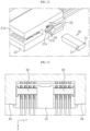
- FIG. 2 is an exploded perspective view showing a connector according to an embodiment of the present disclosure
- FIGS. 3 and 4 are perspective views showing the connector according to an embodiment of the present disclosure before and after being fastened to a circuit board.
- a PCB direct connector 5 is connected directly to a circuit board 4 without a male connector, unlike an existing method where a female connector is inserted into a male connector of a circuit board 4 for the connection to the circuit board 4. In this case, the production cost of the male connector and the process cost of mounting the male connector to the circuit board 4 may be reduced.
- the PCB direct connector 5 includes terminal members 10, a connector housing 20 and a retainer 30.
- the terminal members 10 are electrically conductive metallic components used to easily connect signal transmission cables 6 to conductive patterns of the circuit board 4.
- the terminal members 10 are assembled to the connector housing 20 in a two-row structure.
- the terminal members 10 include first-row terminal members 10a and second-row terminal members 10b, and the first-row terminal members 10a and the second-row terminal members 10b are symmetrically arranged to be spaced apart from each other inside the connector housing 20.
- the first-row terminal member 10a contacts an upper conductive pattern 4a provided on the upper surface of the circuit board 4, and the second-row terminal member 10b contacts a lower conductive pattern 4b provided on the lower surface of the circuit board 4, respectively, to transmit different signals to the circuit board 4.
- the conductive patterns 4a, 4b are formed on both surfaces of the circuit board 4 and the terminal members 10 are arranged in two rows inside the connector housing 20 to contact the conductive patterns 4a, 4b as described above, the right and left width of the connector housing 20 may be reduced by half compared to the existing connector housing 20 having a one-row structure.
- first-row terminal members 10a and the second-row terminal members 10b are symmetrically arranged in the same configuration, just one of them will be described.
- the terminal member 10 includes a terminal body 11 and a contact portion 16.
- the terminal body 11 of this embodiment includes a horizontal body 12 extending toward a portion where the signal transmission cable 6 is connected, and a pair of vertical bodies 13, 14 extending in the same direction orthogonal to the horizontal body 12 with a predetermined gap therebetween.
- the signal transmission cable 6 may be connected to the horizontal body 12, and the retainer 30 may be interposed later in a fitting space S formed between the pair of vertical bodies 13, 14.
- the retainer 30 may prevent the terminal members 10 from moving inside the connector housing 20 as explained in detail later.
- the contact portion 16 may be provided in a cantilever shape extending from the terminal body 11 and having at least a portion curved to elastically contact the surface of the circuit board 4.
- the contact portions 16 of the terminal members 10 may contact the upper conductive patterns 4a and the lower conductive patterns 4b of the circuit board 4, respectively, when the direct connector 5 is mounted on the circuit board 4.
- the interval between the curved portion of the contact portion 16 of the first-row terminal member 10a and the curved portion of the contact portion 16 of the second-row terminal member 10b is smaller than the thickness of the circuit board 4 so that the contact portions 16 may elastically contact the upper conductive patterns 4a and the lower conductive patterns 4b.
- the direct connector 5 may be fastened to the circuit board 4 without a male connector, but the direct connector 5 may also be applied to a circuit board 4 in which a predetermined fastening hole 4e and conductive patterns are provided at both surfaces thereof in advance.
- a connector connection portion 4c one side of an end of the circuit board 4 having the conductive patterns 4a, 4b at both surfaces thereof will be referred to as a connector connection portion 4c.
- the connector connection portion 4c is preferably formed concave into the circuit board 4 as shown in FIG. 3 .
- an insert limit plate 20c extending along the left and right width of the connector housing 20 to partially block the outlet of the insert holes 23 may be provided to a border between the front portion 20a and the rear portion 20b of the connector housing 20.
- the contact portions 16 may move out through the insert holes 23 and the gap between the insert limit plate 20c and be disposed at the front portion 20a of the connector housing 20, and the terminal bodies may be blocked by the insert limit plate 20c and thus disposed at the rear portion 20b of the connector housing 20.
- the connector connection portion 4c of the circuit board 4 may be inserted up to the front portion 20a of the connector housing 20, and the upper surface and the lower surface of the connector connection portion 4c may elastically contact the contact portion 16 of the first-row terminal member 10a and the contact portion 16 of the second-row terminal member 10b.
- the contact portions 16 of the different terminal members 10 neighboring in the Y-axis direction are partially inserted into guide grooves provided at the upper plate 21 and the lower plate 22 of the front portion 20a of the connector housing 20, respectively, to maintain the creepage distance constant, thereby preventing a short circuit.
- the latch 24 is hooked to the fastening hole 4e provided in the circuit board 4 in advance to hold the connector housing 20 not to be released from the connector connection portion 4c in a reverse direction (+X-axis direction).
- the upper plate 21 of the connector housing 20 is divided into a first upper plate 21 and a second upper plate 21, and the latch 24 is provided between the first upper plate 21 and the second upper plate 21.
- the latch 24 includes a shaft 24a protruding orthogonal to the upper surface of the lower plate 22, a latch plate 24b connected to the shaft 24a and extending parallel to the upper plate 21, and a hook 24c provided at one end of the latch plate 24b.
- the hook 24c may be vertically inserted into the fastening hole 4e provided at the circuit board 4 and be bent orthogonal to the latch plate 24b so as to be hooked in the fastening hole 4e.
- the latch plate 24b is supported by the shaft 24a at a predetermined gap away from the lower plate 22, and the shaft 24a is located approximately at the center of the latch plate 24b.
- the latch plate 24b may make a seesawing operation based on the shaft 24a. If the latch 24 is used, when it is intended to remove the connector housing 20 from the circuit board 4, a user may simply press the other end of the latch plate 24b to release the hooking between the hook 24c and the fastening hole 4e and then pull the connector housing 20 in the reverse direction.
- the substrate holding rib 25 holds the connector housing 20 not to move in the upper, lower, left and right directions ( ⁇ Y-axis and ⁇ Z-axis directions) relative to the circuit board 4.
- the circuit board 4 is configured such that the substrate holding rib 25 may be applied thereto. That is, the circuit board 4 is assumed such that the connector connection portion 4c has a width corresponding to the upper plate 21 and the lower plate 22 of the connector housing 20 and is concavely recessed into the circuit board 4.
- the substrate holding ribs 25 are located at both side surfaces of the connector housing 20 and have an inner width corresponding to the thickness of the circuit board 4 such that the end portions of the circuit board 4 adjacent to both sides of the connector connection portion 4c are fitted therein.
- the end portion of the circuit board 4 will be referred to as a rib connection portion 4d.
- the connector housing 20 When the front portion 20a of the connector housing 20 is pushed into the connector connection portion 4c of the circuit board 4, since the rib connection portions 4d are fitted into the substrate holding ribs 25, the connector housing 20 may be tightly fixed to the circuit board 4.
- the substrate holding ribs 25 may be provided at the rear portion 20b of the connector housing 20, namely at the rear portions 20b of the upper plate 21 and the lower plate 22 whose side surfaces are blocked.
- the rear portion 20b of the connector housing 20 is tightly interposed in the space between the rib connection portions 4d so that both side surfaces thereof are supported in the left and right direction by the rib connection portion 4d.
- the connector housing 20 may be fixed not to move in the left and right direction ( ⁇ Y-axis direction) with respect to the circuit board 4 even if there is vibration or impact.
- the substrate holding ribs 25 have an inlet 25a having a width greater than the thickness of the circuit board 4.
- the inlet 25a may have a width gradually decreasing in a direction along which the end of the circuit board 4 is inserted. If the inlet 25a of the substrate holding rib 25 is provided as above, the inlet 25a of the substrate holding rib 25 having a greater width may be easily matched with the front end of the rib connection portion 4d. In addition, even if the front end of the rib connection portion 4d is slightly misaligned from the center of the inlet 25a of the substrate holding rib 25 while being fitted, since the width of the inlet 25a gradually decreases, the rib connection portion 4d may be guided suitable for the inner width of the substrate holding rib 25. Thus, according to the configuration of the substrate holding rib 25, the direct connector 5 may be accurately aligned and mounted to the circuit board 4.
- the direct connector 5 is a connector for connecting to the BMS circuit board 4 applied to a battery pack for a vehicle, and further includes a retainer 30 for holding the terminal members 10 not to move.
- the retainer 30 may play a role of holding the terminal members 10 not to move in the positive and reverse directions ( ⁇ X-axis direction) and supporting the first-row terminal members 10a and the second-row terminal members 10b in the up and down directions ( ⁇ Z-axis direction) not to be shorted.
- a side hole 26 communicating with the fitting space S surrounded by the terminal bodies 11 of the first-row terminal members 10a and the terminal bodies 11 of the second-row terminal members 10b disposed in the insert holes 23 may be provided to at least one side surface of the connector housing.
- the side hole 26 is formed in both side surfaces of the connector housing to communicate with the insert holes 23 in an intersecting direction.
- the retainer 30 may be inserted into the side surface of the connector housing 20 one by one (in the Y-axis direction) through the side hole 26 and is interposed in the fitting space S formed between the first-row terminal body 11 and the second-row terminal body 11 disposed in the insert hole 23.
- the upper plate 21 of the connector housing 20 of this embodiment is divided into the first upper plate 21 and the second upper plate 21 with the latch 24 being interposed therebetween, and the terminal members 10 are also divided into a first group and a second group with the latch 24 being interposed therebetween.
- two side holes 26 are formed, one in each of both side surfaces of the connector housing 20, and two retainers 30 are used to fix the terminal members 10 of the first group and the second group.
- the two side holes 26 may be in communication with each other, and thus it is possible to extend one retainer 30 long so that the terminal members 10 of the first group and the second group are integrally fixed using a single retainer 30.
- the retainer 30 includes a terminal support 32 and a stopper 31.
- the terminal support 32 is interposed in the connector housing 20 through the side hole 26 to support the terminal members 10, and the stopper 31 protrudes on one side of the terminal support 32 to limit an insertion depth of the retainer 30.
- the stopper 31 may be hooked around the inlet of the side hole 26.
- a plurality of grooves formed by depressing a surface may be provided around the side hole 26.
- the grooves located to the left and right of the inlet of the side hole 26 are stopper placing grooves 27a, and the grooves located at the top and bottom thereof are tool grooves 27b.
- the retainer 30 may be inserted into the side hole 26 until the stopper 31 engages with the stopper placing groove 27a. That is, the insertion depth of the retainer 30 into the side hole 26 may be limited as the stopper 31 is caught by the stopper placing groove 27a.
- the retainer 30 of this embodiment since the stopper 31 is provided at one end thereof, the retainer 30 may be inserted into the side hole 26 until one end of the retainer 30 is located on the same plane as the side surface of the connector housing 20. In other words, the retainer 30 fully inserted into the side hole 26 may be regarded as being buried in the side surface of the connector housing 20.
- the connector since the terminal members 10 may be assembled in two rows in the connector housing 20, the connector may be implemented to have a half size compared to the existing connector, and also it is possible to prevent the connector from being separated or erroneously contacted even under the vibration and shock conditions.
- the connector housing 20 and the retainer 30 of the direct connector 5 are assembled and disassembled in a simple way, components the connector may be easily maintained and managed when necessary.
Landscapes
- Coupling Device And Connection With Printed Circuit (AREA)
- Details Of Connecting Devices For Male And Female Coupling (AREA)
- Connector Housings Or Holding Contact Members (AREA)
Claims (9)
- PCB-Direktverbinder (5), welcher direkt an einer Leiterplatte (4) montierbar ist, wobei der PCB-Direktverbinder umfasst:Anschlusselemente (10), welche derart in zwei Reihen angeordnet sind, dass sie obere Leiterbilder bzw. untere Leiterbilder kontaktieren, welche an einer oberen Fläche und einer unteren Fläche der Leiterplatte bereitgestellt sind; undein Verbindergehäuse (20), welches dazu eingerichtet ist, die Anschlusselemente darin aufzunehmen und zu ermöglichen, dass ein Verbinderverbindungsabschnitt, welcher an einer Seite eines Endes der Leiterplatte gebildet ist, in das Verbindergehäuse gepasst und davon gelöst werden kann,wobei das Verbindergehäuse eine obere Platte (21) und eine untere Platte (22) umfasst,wobei vordere Abschnitte der oberen Platte und der unteren Platte wenigstens um eine Dicke der Leiterplatte voneinander beabstandet sind, so dass der Verbinderverbindungsabschnitt bis zu einer vorbestimmten Tiefe dazwischen eingesetzt ist, und hintere Abschnitte der oberen Platte und der unteren Platte derart miteinander verbunden sind, dass sie einen einzigen Körper bilden,wobei die obere Platte des Verbindergehäuses in zwei Teile geteilt ist, welche eine erste obere Platte (21a) und eine zweite obere Platte (21b) umfassen, und ein Riegel (24) zwischen der ersten oberen Platte und der zweiten oberen Platte bereitgestellt ist,wobei der Riegel einen Haken aufweist, welcher derart an einem Ende davon bereitgestellt ist, dass er in einem Befestigungsloch eingehakt ist, welches im Voraus in der Leiterplatte bereitgestellt worden ist,wobei an beiden Seitenflächen des Verbindergehäuses davon vorstehende Substrathalterippen (25) positioniert sind, wobei die Substrathalterippen eine innere Breite aufweisen, welche einer Dicke der Leiterplatte entspricht, und wobei die Substrathalterippen dazu eingerichtet sind, auf Basis des Verbinderverbindungsabschnitts an beiden Seiten in Enden der Leiterplatte gepasst zu sein,wobei die Substrathalterippen an den hinteren Abschnitten der oberen Platte und der unteren Platte bereitgestellt sind undwobei die Substrathalterippen Einlässe aufweisen, welche mit einer Breite gebildet sind, die größer ist als die Dicke der Leiterplatte, und wobei die Breite der Einlässe in einer Richtung, entlang welcher ein Ende der Leiterplatte eingesetzt wird, allmählich abnimmt.
- PCB-Direktverbinder nach Anspruch 1,
wobei die hinteren Abschnitte der oberen Platte und der unteren Platte Einsatzlöcher (23) aufweisen, in welche die Anschlusselemente derart in zwei Reihen eingesetzt sind, dass in jedem Einsatzloch zwei Anschlusselemente eingesetzt sind. - PCB-Direktverbinder nach Anspruch 2,
wobei die Anschlusselemente umfassen:einen Anschlusskörper (11), welcher einen horizontalen Körper (12), der derart gebildet ist, dass er sich in Richtung eines Abschnitts erstreckt, in welchem ein Signalübertragungskabel (6) verbunden ist, und ein Paar von vertikalen Körpern (13, 14) aufweist, welche derart gebildet sind, dass sie sich in der gleichen Richtung mit einem vorbestimmten Spalt dazwischen orthogonal zu dem horizontalen Körper erstrecken, wobei der Anschlusskörper in dem Einsatzloch eingefügt ist; undeinen Kontaktabschnitt (16), welcher derart gebildet ist, dass er sich derart von dem Anschlusskörper erstreckt, dass wenigstens ein Teil des Kontaktabschnitts eine gekrümmte Form aufweist, um die obere Fläche oder die untere Fläche der Leiterplatte elastisch zu kontaktieren, wobei der Kontaktabschnitt an einem vorderen Abschnitt (20a) des Verbindergehäuses eingefügt ist. - PCB-Direktverbinder nach Anspruch 3,wobei die Anschlusselemente Erste-Reihe-Anschlusselemente und Zweite-Reihe-Anschlusselemente umfassen, welche symmetrisch innerhalb des Verbindergehäuses angeordnet sind,wobei das Verbindergehäuse ein Seitenloch (26) aufweist, welches in wenigstes einer Seitenfläche davon in einer Richtung gebildet ist, welche sich mit den Einsatzlöchern schneidet, um mit einem Raum zu kommunizieren, welcher durch Anschlusskörper der Erste-Reihe-Anschlusselemente und Anschlusskörper der Zweite-Reihe-Anschlusselemente umgeben ist, undwobei der PCB-Direktverbinder ferner einen Halter (30) umfasst, welcher derart in das Seitenloch eingesetzt ist, dass er die Erste-Reihe-Anschlusselemente und die Zweite-Reihe-Anschlusselemente integral fixiert.
- PCB-Direktverbinder nach Anspruch 4,wobei das Verbindergehäuse eine Mehrzahl von Nuten aufweist, welche durch ein Vertiefen einer Fläche um die Seitenlöcher herum gebildet sind, undwobei der Halter einen Stopper umfasst, welcher dazu eingerichtet ist, mit einem Teil der Mehrzahl von Nuten in Eingriff zu stehen.
- PCB-Direktverbinder nach Anspruch 1,
wobei der Riegel umfasst:einen Schaft (24a), welcher dazu eingerichtet ist, orthogonal zu einer oberen Fläche der unteren Platte vorzustehen, welche zwischen der ersten oberen Platte und der zweiten oberen Platte positioniert ist; undeine Riegelplatte (24b), welche derart eingerichtet ist, dass sie den Haken aufweist und sich parallel zu der oberen Platte erstreckt, wobei die Riegelplatte derart mit dem Schaft verbunden ist, dass sie auf Basis des Schafts einen wippenden Vorgang vollzieht. - PCB-Direktverbinder nach Anspruch 2, ferner umfassend:
eine Einsatzbegrenzungsplatte (20c), welche derart an einer Grenze eines vorderen Abschnitts (20a) und eines hinteren Abschnitts (20b) des Verbindergehäuses bereitgestellt ist, dass sie sich entlang einer Links-Rechts-Breite des Verbindergehäuses erstreckt und eine vorbestimmte Wand zum teilweisen Blockieren von Auslässen der Einsatzlöcher bildet. - PCB-Direktverbinder nach Anspruch 5,
wobei der Halter ferner eine Anschlusshalterung umfasst, welche in die Seitenlöcher eingesetzt ist und in dem Verbindergehäuse eingefügt ist, und wobei der Stopper an einer Seite der Anschlusshalterung in einer Richtung vorsteht, welche sich mit der Erstreckungsrichtung der Anschlusshalterung schneidet. - PCB-Direktverbinder nach Anspruch 5,
wobei die Mehrzahl von Nuten des Verbindergehäuses wenigstens eine Stopperplatzierungsnut (27a), welche derart gebildet ist, dass sie mit dem Stopper in Eingriff steht, und wenigstens eine Werkzeugnut (27b), welche derart bereitgestellt ist, dass ein vorbestimmtes Werkzeug darin eingesetzt werden kann, in einer zu der Stopperplatzierungsnut benachbarten Position umfasst.
Applications Claiming Priority (2)
| Application Number | Priority Date | Filing Date | Title |
|---|---|---|---|
| KR1020180067735A KR102300060B1 (ko) | 2018-06-12 | 2018-06-12 | 2열 터미널 구조의 pcb 다이렉트 커넥터 |
| PCT/KR2019/005573 WO2019240378A1 (ko) | 2018-06-12 | 2019-05-09 | 2열 터미널 구조의 pcb 다이렉트 커넥터 |
Publications (3)
| Publication Number | Publication Date |
|---|---|
| EP3706255A1 EP3706255A1 (de) | 2020-09-09 |
| EP3706255A4 EP3706255A4 (de) | 2020-12-30 |
| EP3706255B1 true EP3706255B1 (de) | 2025-02-26 |
Family
ID=68842251
Family Applications (1)
| Application Number | Title | Priority Date | Filing Date |
|---|---|---|---|
| EP19818817.9A Active EP3706255B1 (de) | 2018-06-12 | 2019-05-09 | Leiterplattendirektverbinder mit zweireihiger anschlussstruktur |
Country Status (8)
| Country | Link |
|---|---|
| US (1) | US11114788B2 (de) |
| EP (1) | EP3706255B1 (de) |
| JP (1) | JP7049565B2 (de) |
| KR (1) | KR102300060B1 (de) |
| CN (1) | CN111684669B (de) |
| ES (1) | ES3017064T3 (de) |
| HU (1) | HUE070689T2 (de) |
| WO (1) | WO2019240378A1 (de) |
Families Citing this family (8)
| Publication number | Priority date | Publication date | Assignee | Title |
|---|---|---|---|---|
| KR102332605B1 (ko) * | 2018-05-31 | 2021-11-26 | 주식회사 엘지에너지솔루션 | Pcb 다이렉트 커넥터 |
| KR102300060B1 (ko) * | 2018-06-12 | 2021-09-08 | 주식회사 엘지에너지솔루션 | 2열 터미널 구조의 pcb 다이렉트 커넥터 |
| US10892579B2 (en) * | 2019-02-25 | 2021-01-12 | J.S.T. Corporation | Female terminal position assurance (TPA) device for a connector and method for assembling thereof |
| US11088481B2 (en) * | 2019-03-13 | 2021-08-10 | 3M Innovative Properties Company | Scalable high-speed electrical cable assembly |
| US11710918B2 (en) * | 2020-06-19 | 2023-07-25 | Te Connectivity Solutions Gmbh | Cable receptacle connector for a communication system |
| FR3116887B1 (fr) * | 2020-11-30 | 2022-12-02 | Valeo Vision | Module de connexion électrique et dispositif d'éclairage automobile |
| KR20230052072A (ko) * | 2021-10-12 | 2023-04-19 | 현대자동차주식회사 | 연료 전지용 셀 모니터링 커넥터 |
| CN114447666A (zh) * | 2021-12-30 | 2022-05-06 | 通力科技股份有限公司 | 一种连接器、金属弹片及pcb板连接结构 |
Citations (2)
| Publication number | Priority date | Publication date | Assignee | Title |
|---|---|---|---|---|
| KR20180039936A (ko) * | 2016-10-11 | 2018-04-19 | (주)우주일렉트로닉스 | 기판 접속용 커넥터 |
| WO2018101910A1 (en) * | 2016-11-29 | 2018-06-07 | Molex, Llc | Low profile edge connector and system using same |
Family Cites Families (24)
| Publication number | Priority date | Publication date | Assignee | Title |
|---|---|---|---|---|
| JPS541595Y2 (de) | 1973-10-12 | 1979-01-24 | ||
| JPS5498986A (en) * | 1978-01-20 | 1979-08-04 | Nippon Telegr & Teleph Corp <Ntt> | Connector for printed circuit board |
| US4400049A (en) * | 1981-08-12 | 1983-08-23 | Ncr Corporation | Connector for interconnecting circuit boards |
| JPH05211082A (ja) * | 1992-01-30 | 1993-08-20 | Aisin Seiki Co Ltd | プリント配線板とコネクタの接続構造 |
| JPH0660082U (ja) | 1993-01-26 | 1994-08-19 | ミツミ電機株式会社 | 配線基板接続構造 |
| JPH07312265A (ja) * | 1994-05-18 | 1995-11-28 | Yazaki Corp | コネクタ取付構造 |
| JP2002324607A (ja) | 2001-04-25 | 2002-11-08 | Matsushita Electric Ind Co Ltd | フレキシブルプリント基板の中継コネクタ |
| JP2006236657A (ja) | 2005-02-23 | 2006-09-07 | Nec Corp | コネクタ装置 |
| KR101111911B1 (ko) | 2005-06-28 | 2012-02-14 | 삼성전자주식회사 | 기판조립체 |
| HUE035655T2 (en) | 2005-08-05 | 2018-05-28 | Araim Pharmaceuticals Inc | Tissue protective peptides and their use |
| JP2007214087A (ja) * | 2006-02-13 | 2007-08-23 | Fujikura Ltd | コネクタ |
| JP2009043489A (ja) | 2007-08-07 | 2009-02-26 | Japan Aviation Electronics Industry Ltd | コネクタ |
| KR20100046911A (ko) | 2008-10-28 | 2010-05-07 | 주식회사 유라코퍼레이션 | 자동차용 리테이너 |
| KR20100110023A (ko) | 2009-04-02 | 2010-10-12 | 삼성전기주식회사 | 커넥터 |
| JP5110403B2 (ja) | 2010-01-15 | 2012-12-26 | 第一精工株式会社 | 電気コネクタ及び電気コネクタ組立体 |
| JP5152221B2 (ja) | 2010-02-19 | 2013-02-27 | 第一精工株式会社 | 電気コネクタ及び電気コネクタ組立体 |
| JP2012243562A (ja) | 2011-05-19 | 2012-12-10 | Auto Network Gijutsu Kenkyusho:Kk | コネクタ端子及びこのコネクタ端子を含むカードエッジ型コネクタ |
| KR101562810B1 (ko) | 2014-05-29 | 2015-11-09 | 케이유엠 주식회사 | 평판 케이블 커넥터 |
| WO2015183951A1 (en) | 2014-05-30 | 2015-12-03 | Molex Incorporated | Electrical connector with terminal holder |
| JP6531292B2 (ja) | 2015-01-06 | 2019-06-19 | アール・ビー・コントロールズ株式会社 | プリント配線基板 |
| KR101750485B1 (ko) | 2015-01-08 | 2017-06-23 | 주식회사 엘지화학 | 커넥터 엣지를 포함하고 있는 pcb |
| CN208189901U (zh) | 2018-05-08 | 2018-12-04 | 许琳燕 | 一种兼容充电与数据传输的连接器 |
| KR102332605B1 (ko) * | 2018-05-31 | 2021-11-26 | 주식회사 엘지에너지솔루션 | Pcb 다이렉트 커넥터 |
| KR102300060B1 (ko) * | 2018-06-12 | 2021-09-08 | 주식회사 엘지에너지솔루션 | 2열 터미널 구조의 pcb 다이렉트 커넥터 |
-
2018
- 2018-06-12 KR KR1020180067735A patent/KR102300060B1/ko active Active
-
2019
- 2019-05-09 EP EP19818817.9A patent/EP3706255B1/de active Active
- 2019-05-09 WO PCT/KR2019/005573 patent/WO2019240378A1/ko not_active Ceased
- 2019-05-09 HU HUE19818817A patent/HUE070689T2/hu unknown
- 2019-05-09 CN CN201980011670.4A patent/CN111684669B/zh active Active
- 2019-05-09 ES ES19818817T patent/ES3017064T3/es active Active
- 2019-05-09 US US16/759,423 patent/US11114788B2/en active Active
- 2019-05-09 JP JP2020522949A patent/JP7049565B2/ja active Active
Patent Citations (2)
| Publication number | Priority date | Publication date | Assignee | Title |
|---|---|---|---|---|
| KR20180039936A (ko) * | 2016-10-11 | 2018-04-19 | (주)우주일렉트로닉스 | 기판 접속용 커넥터 |
| WO2018101910A1 (en) * | 2016-11-29 | 2018-06-07 | Molex, Llc | Low profile edge connector and system using same |
Also Published As
| Publication number | Publication date |
|---|---|
| ES3017064T3 (en) | 2025-05-12 |
| WO2019240378A1 (ko) | 2019-12-19 |
| HUE070689T2 (hu) | 2025-06-28 |
| JP7049565B2 (ja) | 2022-04-07 |
| EP3706255A4 (de) | 2020-12-30 |
| US11114788B2 (en) | 2021-09-07 |
| CN111684669B (zh) | 2022-07-15 |
| KR20190140783A (ko) | 2019-12-20 |
| JP2021501440A (ja) | 2021-01-14 |
| CN111684669A (zh) | 2020-09-18 |
| KR102300060B1 (ko) | 2021-09-08 |
| EP3706255A1 (de) | 2020-09-09 |
| US20200274275A1 (en) | 2020-08-27 |
Similar Documents
| Publication | Publication Date | Title |
|---|---|---|
| EP3683896B1 (de) | Direktverbinder für leiterplatten | |
| US11114788B2 (en) | PCB direct connector having two-row terminal structure | |
| EP3691041B1 (de) | Vertikaler direkter leiterplattensteckverbinder | |
| US8292669B2 (en) | Electrical connector having contact modules | |
| CN102185194B (zh) | 具有接触器模块的电连接器 | |
| CN108448302A (zh) | 电连接器组件及其转接件 | |
| CN102201622A (zh) | 电连接器及其组件 | |
| CN111542970A (zh) | 可扩展连接器组件 | |
| US11114787B2 (en) | Terminal for connector mounted to printed circuit board and connector supporting said terminal | |
| US7566244B1 (en) | Supporting a pluggable transceiver module | |
| US20110300761A1 (en) | Electrical adapter | |
| EP2347476B1 (de) | Verbinder mit federzungen zum halten eines kontaktmoduls | |
| KR102725757B1 (ko) | 인쇄회로기판용 커넥터 | |
| EP3109945B1 (de) | Leitungskonzentrator | |
| CN118281602A (zh) | 背板系统及其制备方法和机柜 | |
| JP2024159644A (ja) | プリント回路基板アセンブリおよびコネクタアセンブリ | |
| WO2009040613A1 (en) | Electrical connector and connection system |
Legal Events
| Date | Code | Title | Description |
|---|---|---|---|
| STAA | Information on the status of an ep patent application or granted ep patent |
Free format text: STATUS: THE INTERNATIONAL PUBLICATION HAS BEEN MADE |
|
| PUAI | Public reference made under article 153(3) epc to a published international application that has entered the european phase |
Free format text: ORIGINAL CODE: 0009012 |
|
| STAA | Information on the status of an ep patent application or granted ep patent |
Free format text: STATUS: REQUEST FOR EXAMINATION WAS MADE |
|
| 17P | Request for examination filed |
Effective date: 20200604 |
|
| AK | Designated contracting states |
Kind code of ref document: A1 Designated state(s): AL AT BE BG CH CY CZ DE DK EE ES FI FR GB GR HR HU IE IS IT LI LT LU LV MC MK MT NL NO PL PT RO RS SE SI SK SM TR |
|
| AX | Request for extension of the european patent |
Extension state: BA ME |
|
| A4 | Supplementary search report drawn up and despatched |
Effective date: 20201126 |
|
| RIC1 | Information provided on ipc code assigned before grant |
Ipc: H01R 13/629 20060101AFI20201120BHEP Ipc: H01R 12/71 20110101ALI20201120BHEP Ipc: H01R 12/72 20110101ALI20201120BHEP Ipc: H01R 12/89 20110101ALI20201120BHEP Ipc: H01R 13/436 20060101ALI20201120BHEP Ipc: H01R 13/627 20060101ALI20201120BHEP Ipc: H01R 13/24 20060101ALI20201120BHEP Ipc: H01R 13/26 20060101ALI20201120BHEP Ipc: H01R 12/77 20110101ALI20201120BHEP Ipc: H01R 13/631 20060101ALI20201120BHEP |
|
| DAV | Request for validation of the european patent (deleted) | ||
| DAX | Request for extension of the european patent (deleted) | ||
| RAP1 | Party data changed (applicant data changed or rights of an application transferred) |
Owner name: LG ENERGY SOLUTION LTD. |
|
| STAA | Information on the status of an ep patent application or granted ep patent |
Free format text: STATUS: EXAMINATION IS IN PROGRESS |
|
| 17Q | First examination report despatched |
Effective date: 20220121 |
|
| RAP3 | Party data changed (applicant data changed or rights of an application transferred) |
Owner name: LG ENERGY SOLUTION, LTD. |
|
| GRAP | Despatch of communication of intention to grant a patent |
Free format text: ORIGINAL CODE: EPIDOSNIGR1 |
|
| STAA | Information on the status of an ep patent application or granted ep patent |
Free format text: STATUS: GRANT OF PATENT IS INTENDED |
|
| INTG | Intention to grant announced |
Effective date: 20241114 |
|
| GRAS | Grant fee paid |
Free format text: ORIGINAL CODE: EPIDOSNIGR3 |
|
| P01 | Opt-out of the competence of the unified patent court (upc) registered |
Free format text: CASE NUMBER: APP_65644/2024 Effective date: 20241212 |
|
| GRAA | (expected) grant |
Free format text: ORIGINAL CODE: 0009210 |
|
| STAA | Information on the status of an ep patent application or granted ep patent |
Free format text: STATUS: THE PATENT HAS BEEN GRANTED |
|
| AK | Designated contracting states |
Kind code of ref document: B1 Designated state(s): AL AT BE BG CH CY CZ DE DK EE ES FI FR GB GR HR HU IE IS IT LI LT LU LV MC MK MT NL NO PL PT RO RS SE SI SK SM TR |
|
| REG | Reference to a national code |
Ref country code: GB Ref legal event code: FG4D |
|
| REG | Reference to a national code |
Ref country code: CH Ref legal event code: EP |
|
| REG | Reference to a national code |
Ref country code: DE Ref legal event code: R096 Ref document number: 602019066573 Country of ref document: DE |
|
| REG | Reference to a national code |
Ref country code: IE Ref legal event code: FG4D |
|
| REG | Reference to a national code |
Ref country code: ES Ref legal event code: FG2A Ref document number: 3017064 Country of ref document: ES Kind code of ref document: T3 Effective date: 20250512 |
|
| REG | Reference to a national code |
Ref country code: HU Ref legal event code: AG4A Ref document number: E070689 Country of ref document: HU |
|
| REG | Reference to a national code |
Ref country code: NL Ref legal event code: MP Effective date: 20250226 |
|
| PG25 | Lapsed in a contracting state [announced via postgrant information from national office to epo] |
Ref country code: RS Free format text: LAPSE BECAUSE OF FAILURE TO SUBMIT A TRANSLATION OF THE DESCRIPTION OR TO PAY THE FEE WITHIN THE PRESCRIBED TIME-LIMIT Effective date: 20250526 |
|
| PG25 | Lapsed in a contracting state [announced via postgrant information from national office to epo] |
Ref country code: FI Free format text: LAPSE BECAUSE OF FAILURE TO SUBMIT A TRANSLATION OF THE DESCRIPTION OR TO PAY THE FEE WITHIN THE PRESCRIBED TIME-LIMIT Effective date: 20250226 |
|
| PG25 | Lapsed in a contracting state [announced via postgrant information from national office to epo] |
Ref country code: PL Free format text: LAPSE BECAUSE OF FAILURE TO SUBMIT A TRANSLATION OF THE DESCRIPTION OR TO PAY THE FEE WITHIN THE PRESCRIBED TIME-LIMIT Effective date: 20250226 |
|
| PGFP | Annual fee paid to national office [announced via postgrant information from national office to epo] |
Ref country code: DE Payment date: 20250422 Year of fee payment: 7 |
|
| PGFP | Annual fee paid to national office [announced via postgrant information from national office to epo] |
Ref country code: ES Payment date: 20250613 Year of fee payment: 7 |
|
| REG | Reference to a national code |
Ref country code: LT Ref legal event code: MG9D |
|
| PG25 | Lapsed in a contracting state [announced via postgrant information from national office to epo] |
Ref country code: NO Free format text: LAPSE BECAUSE OF FAILURE TO SUBMIT A TRANSLATION OF THE DESCRIPTION OR TO PAY THE FEE WITHIN THE PRESCRIBED TIME-LIMIT Effective date: 20250526 Ref country code: IS Free format text: LAPSE BECAUSE OF FAILURE TO SUBMIT A TRANSLATION OF THE DESCRIPTION OR TO PAY THE FEE WITHIN THE PRESCRIBED TIME-LIMIT Effective date: 20250626 |
|
| PGFP | Annual fee paid to national office [announced via postgrant information from national office to epo] |
Ref country code: HU Payment date: 20250526 Year of fee payment: 7 |
|
| PG25 | Lapsed in a contracting state [announced via postgrant information from national office to epo] |
Ref country code: NL Free format text: LAPSE BECAUSE OF FAILURE TO SUBMIT A TRANSLATION OF THE DESCRIPTION OR TO PAY THE FEE WITHIN THE PRESCRIBED TIME-LIMIT Effective date: 20250226 |
|
| PGFP | Annual fee paid to national office [announced via postgrant information from national office to epo] |
Ref country code: BE Payment date: 20250508 Year of fee payment: 7 |
|
| PG25 | Lapsed in a contracting state [announced via postgrant information from national office to epo] |
Ref country code: HR Free format text: LAPSE BECAUSE OF FAILURE TO SUBMIT A TRANSLATION OF THE DESCRIPTION OR TO PAY THE FEE WITHIN THE PRESCRIBED TIME-LIMIT Effective date: 20250226 |
|
| PG25 | Lapsed in a contracting state [announced via postgrant information from national office to epo] |
Ref country code: PT Free format text: LAPSE BECAUSE OF FAILURE TO SUBMIT A TRANSLATION OF THE DESCRIPTION OR TO PAY THE FEE WITHIN THE PRESCRIBED TIME-LIMIT Effective date: 20250626 Ref country code: LV Free format text: LAPSE BECAUSE OF FAILURE TO SUBMIT A TRANSLATION OF THE DESCRIPTION OR TO PAY THE FEE WITHIN THE PRESCRIBED TIME-LIMIT Effective date: 20250226 |
|
| PGFP | Annual fee paid to national office [announced via postgrant information from national office to epo] |
Ref country code: FR Payment date: 20250422 Year of fee payment: 7 |
|
| PG25 | Lapsed in a contracting state [announced via postgrant information from national office to epo] |
Ref country code: BG Free format text: LAPSE BECAUSE OF FAILURE TO SUBMIT A TRANSLATION OF THE DESCRIPTION OR TO PAY THE FEE WITHIN THE PRESCRIBED TIME-LIMIT Effective date: 20250226 Ref country code: GR Free format text: LAPSE BECAUSE OF FAILURE TO SUBMIT A TRANSLATION OF THE DESCRIPTION OR TO PAY THE FEE WITHIN THE PRESCRIBED TIME-LIMIT Effective date: 20250527 |
|
| REG | Reference to a national code |
Ref country code: AT Ref legal event code: MK05 Ref document number: 1771626 Country of ref document: AT Kind code of ref document: T Effective date: 20250226 |
|
| PG25 | Lapsed in a contracting state [announced via postgrant information from national office to epo] |
Ref country code: SE Free format text: LAPSE BECAUSE OF FAILURE TO SUBMIT A TRANSLATION OF THE DESCRIPTION OR TO PAY THE FEE WITHIN THE PRESCRIBED TIME-LIMIT Effective date: 20250226 |
|
| PG25 | Lapsed in a contracting state [announced via postgrant information from national office to epo] |
Ref country code: SM Free format text: LAPSE BECAUSE OF FAILURE TO SUBMIT A TRANSLATION OF THE DESCRIPTION OR TO PAY THE FEE WITHIN THE PRESCRIBED TIME-LIMIT Effective date: 20250226 |
|
| PG25 | Lapsed in a contracting state [announced via postgrant information from national office to epo] |
Ref country code: DK Free format text: LAPSE BECAUSE OF FAILURE TO SUBMIT A TRANSLATION OF THE DESCRIPTION OR TO PAY THE FEE WITHIN THE PRESCRIBED TIME-LIMIT Effective date: 20250226 |
|
| PG25 | Lapsed in a contracting state [announced via postgrant information from national office to epo] |
Ref country code: IT Free format text: LAPSE BECAUSE OF FAILURE TO SUBMIT A TRANSLATION OF THE DESCRIPTION OR TO PAY THE FEE WITHIN THE PRESCRIBED TIME-LIMIT Effective date: 20250226 |
|
| PG25 | Lapsed in a contracting state [announced via postgrant information from national office to epo] |
Ref country code: AT Free format text: LAPSE BECAUSE OF FAILURE TO SUBMIT A TRANSLATION OF THE DESCRIPTION OR TO PAY THE FEE WITHIN THE PRESCRIBED TIME-LIMIT Effective date: 20250226 |
|
| PG25 | Lapsed in a contracting state [announced via postgrant information from national office to epo] |
Ref country code: CZ Free format text: LAPSE BECAUSE OF FAILURE TO SUBMIT A TRANSLATION OF THE DESCRIPTION OR TO PAY THE FEE WITHIN THE PRESCRIBED TIME-LIMIT Effective date: 20250226 Ref country code: EE Free format text: LAPSE BECAUSE OF FAILURE TO SUBMIT A TRANSLATION OF THE DESCRIPTION OR TO PAY THE FEE WITHIN THE PRESCRIBED TIME-LIMIT Effective date: 20250226 |
|
| PG25 | Lapsed in a contracting state [announced via postgrant information from national office to epo] |
Ref country code: RO Free format text: LAPSE BECAUSE OF FAILURE TO SUBMIT A TRANSLATION OF THE DESCRIPTION OR TO PAY THE FEE WITHIN THE PRESCRIBED TIME-LIMIT Effective date: 20250226 |
|
| PG25 | Lapsed in a contracting state [announced via postgrant information from national office to epo] |
Ref country code: SK Free format text: LAPSE BECAUSE OF FAILURE TO SUBMIT A TRANSLATION OF THE DESCRIPTION OR TO PAY THE FEE WITHIN THE PRESCRIBED TIME-LIMIT Effective date: 20250226 |
|
| REG | Reference to a national code |
Ref country code: DE Ref legal event code: R097 Ref document number: 602019066573 Country of ref document: DE |
|
| REG | Reference to a national code |
Ref country code: CH Ref legal event code: H13 Free format text: ST27 STATUS EVENT CODE: U-0-0-H10-H13 (AS PROVIDED BY THE NATIONAL OFFICE) Effective date: 20251223 |
|
| PLBE | No opposition filed within time limit |
Free format text: ORIGINAL CODE: 0009261 |
|
| STAA | Information on the status of an ep patent application or granted ep patent |
Free format text: STATUS: NO OPPOSITION FILED WITHIN TIME LIMIT |
|
| PG25 | Lapsed in a contracting state [announced via postgrant information from national office to epo] |
Ref country code: LU Free format text: LAPSE BECAUSE OF NON-PAYMENT OF DUE FEES Effective date: 20250509 |
|
| PG25 | Lapsed in a contracting state [announced via postgrant information from national office to epo] |
Ref country code: CH Free format text: LAPSE BECAUSE OF NON-PAYMENT OF DUE FEES Effective date: 20250531 |
|
| PG25 | Lapsed in a contracting state [announced via postgrant information from national office to epo] |
Ref country code: MC Free format text: LAPSE BECAUSE OF FAILURE TO SUBMIT A TRANSLATION OF THE DESCRIPTION OR TO PAY THE FEE WITHIN THE PRESCRIBED TIME-LIMIT Effective date: 20250226 |
|
| 26N | No opposition filed |
Effective date: 20251127 |
|
| PGFP | Annual fee paid to national office [announced via postgrant information from national office to epo] |
Ref country code: GB Payment date: 20260324 Year of fee payment: 8 |
|
| PG25 | Lapsed in a contracting state [announced via postgrant information from national office to epo] |
Ref country code: IE Free format text: LAPSE BECAUSE OF NON-PAYMENT OF DUE FEES Effective date: 20250509 |