EP3690385A1 - Strain gauge and sensor module - Google Patents
Strain gauge and sensor module Download PDFInfo
- Publication number
- EP3690385A1 EP3690385A1 EP18860610.7A EP18860610A EP3690385A1 EP 3690385 A1 EP3690385 A1 EP 3690385A1 EP 18860610 A EP18860610 A EP 18860610A EP 3690385 A1 EP3690385 A1 EP 3690385A1
- Authority
- EP
- European Patent Office
- Prior art keywords
- resistor
- strain gauge
- layer
- substrate
- metallic layer
- Prior art date
- Legal status (The legal status is an assumption and is not a legal conclusion. Google has not performed a legal analysis and makes no representation as to the accuracy of the status listed.)
- Granted
Links
Images





Classifications
-
- G—PHYSICS
- G01—MEASURING; TESTING
- G01L—MEASURING FORCE, STRESS, TORQUE, WORK, MECHANICAL POWER, MECHANICAL EFFICIENCY, OR FLUID PRESSURE
- G01L1/00—Measuring force or stress, in general
- G01L1/20—Measuring force or stress, in general by measuring variations in ohmic resistance of solid materials or of electrically-conductive fluids; by making use of electrokinetic cells, i.e. liquid-containing cells wherein an electrical potential is produced or varied upon the application of stress
- G01L1/22—Measuring force or stress, in general by measuring variations in ohmic resistance of solid materials or of electrically-conductive fluids; by making use of electrokinetic cells, i.e. liquid-containing cells wherein an electrical potential is produced or varied upon the application of stress using resistance strain gauges
- G01L1/2268—Arrangements for correcting or for compensating unwanted effects
-
- G—PHYSICS
- G01—MEASURING; TESTING
- G01B—MEASURING LENGTH, THICKNESS OR SIMILAR LINEAR DIMENSIONS; MEASURING ANGLES; MEASURING AREAS; MEASURING IRREGULARITIES OF SURFACES OR CONTOURS
- G01B7/00—Measuring arrangements characterised by the use of electric or magnetic techniques
- G01B7/16—Measuring arrangements characterised by the use of electric or magnetic techniques for measuring the deformation in a solid, e.g. by resistance strain gauge
- G01B7/18—Measuring arrangements characterised by the use of electric or magnetic techniques for measuring the deformation in a solid, e.g. by resistance strain gauge using change in resistance
-
- C—CHEMISTRY; METALLURGY
- C22—METALLURGY; FERROUS OR NON-FERROUS ALLOYS; TREATMENT OF ALLOYS OR NON-FERROUS METALS
- C22C—ALLOYS
- C22C38/00—Ferrous alloys, e.g. steel alloys
- C22C38/18—Ferrous alloys, e.g. steel alloys containing chromium
- C22C38/40—Ferrous alloys, e.g. steel alloys containing chromium with nickel
- C22C38/42—Ferrous alloys, e.g. steel alloys containing chromium with nickel with copper
-
- G—PHYSICS
- G01—MEASURING; TESTING
- G01B—MEASURING LENGTH, THICKNESS OR SIMILAR LINEAR DIMENSIONS; MEASURING ANGLES; MEASURING AREAS; MEASURING IRREGULARITIES OF SURFACES OR CONTOURS
- G01B7/00—Measuring arrangements characterised by the use of electric or magnetic techniques
- G01B7/16—Measuring arrangements characterised by the use of electric or magnetic techniques for measuring the deformation in a solid, e.g. by resistance strain gauge
-
- G—PHYSICS
- G01—MEASURING; TESTING
- G01B—MEASURING LENGTH, THICKNESS OR SIMILAR LINEAR DIMENSIONS; MEASURING ANGLES; MEASURING AREAS; MEASURING IRREGULARITIES OF SURFACES OR CONTOURS
- G01B7/00—Measuring arrangements characterised by the use of electric or magnetic techniques
- G01B7/16—Measuring arrangements characterised by the use of electric or magnetic techniques for measuring the deformation in a solid, e.g. by resistance strain gauge
- G01B7/18—Measuring arrangements characterised by the use of electric or magnetic techniques for measuring the deformation in a solid, e.g. by resistance strain gauge using change in resistance
- G01B7/20—Measuring arrangements characterised by the use of electric or magnetic techniques for measuring the deformation in a solid, e.g. by resistance strain gauge using change in resistance formed by printed-circuit technique
-
- G—PHYSICS
- G01—MEASURING; TESTING
- G01L—MEASURING FORCE, STRESS, TORQUE, WORK, MECHANICAL POWER, MECHANICAL EFFICIENCY, OR FLUID PRESSURE
- G01L1/00—Measuring force or stress, in general
- G01L1/20—Measuring force or stress, in general by measuring variations in ohmic resistance of solid materials or of electrically-conductive fluids; by making use of electrokinetic cells, i.e. liquid-containing cells wherein an electrical potential is produced or varied upon the application of stress
- G01L1/22—Measuring force or stress, in general by measuring variations in ohmic resistance of solid materials or of electrically-conductive fluids; by making use of electrokinetic cells, i.e. liquid-containing cells wherein an electrical potential is produced or varied upon the application of stress using resistance strain gauges
- G01L1/2287—Measuring force or stress, in general by measuring variations in ohmic resistance of solid materials or of electrically-conductive fluids; by making use of electrokinetic cells, i.e. liquid-containing cells wherein an electrical potential is produced or varied upon the application of stress using resistance strain gauges constructional details of the strain gauges
-
- H—ELECTRICITY
- H01—ELECTRIC ELEMENTS
- H01C—RESISTORS
- H01C1/00—Details
- H01C1/14—Terminals or tapping points specially adapted for resistors; Arrangements of terminals or tapping points on resistors
-
- H—ELECTRICITY
- H01—ELECTRIC ELEMENTS
- H01C—RESISTORS
- H01C17/00—Apparatus or processes specially adapted for manufacturing resistors
- H01C17/06—Apparatus or processes specially adapted for manufacturing resistors adapted for coating resistive material on a base
- H01C17/065—Apparatus or processes specially adapted for manufacturing resistors adapted for coating resistive material on a base by thick film techniques, e.g. serigraphy
- H01C17/06506—Precursor compositions therefor, e.g. pastes, inks, glass frits or green body
- H01C17/06513—Precursor compositions therefor, e.g. pastes, inks, glass frits or green body characterised by the resistive component
- H01C17/06526—Precursor compositions therefor, e.g. pastes, inks, glass frits or green body characterised by the resistive component composed of metals
-
- H—ELECTRICITY
- H01—ELECTRIC ELEMENTS
- H01C—RESISTORS
- H01C3/00—Non-adjustable metal resistors made of wire or ribbon, e.g. coiled, woven or formed as grids
- H01C3/10—Non-adjustable metal resistors made of wire or ribbon, e.g. coiled, woven or formed as grids the resistive element having zig-zag or sinusoidal configuration
- H01C3/12—Non-adjustable metal resistors made of wire or ribbon, e.g. coiled, woven or formed as grids the resistive element having zig-zag or sinusoidal configuration lying in one plane
Definitions
- the present invention relates to a strain gauge and a sensor module.
- a strain gauge is known to be attached to a measured object to detect strain on the measured object.
- the strain gauge includes a resistor that detects strain, and as resistor material, for example, material including Cr (chromium) or Ni (nickel) is used.
- the resistor is formed on a substrate made of, for example, an insulating resin (see, for example, Patent document 1).
- Patent document 1 Japanese Unexamined Patent Application Publication No. 2016-74934
- an object of the present invention is to improve stability of gauge characteristics of a strain gauge including a resistor formed above a flexible substrate.
- a strain gauge includes a flexible substrate; a functional layer formed of a metal, an alloy, or a metal compound, on one surface of the substrate; a resistor formed of material including at least one from among chromium and nickel, on one surface of the functional layer; and an insulating resin layer with which the resistor is coated.
- Fig. 1 is a plan view of an example of a strain gauge according to a first embodiment.
- Fig. 2 is a cross-sectional view of an example of the strain gauge according to the first embodiment, and illustrates a cross section taken along the A-A line in Fig. 1 .
- the strain gauge 1 includes a substrate 10, a functional layer 20, a resistor 30, terminal sections 41, and a cover layer 60. Note that in Fig. 1 , an outer edge of the cover layer 60 is only expressed by a dashed line in order to indicate the resistor 30, for the sake of convenience.
- the side of the substrate 10 where the resistor 30 is provided is referred to as an upper side or one side; and the side of the substrate 10 where the resistor 30 is not provided is referred to as a lower side or another side.
- the surface on the side where the resistor 30 is provided is referred to as one surface or an upper surface; and the surface on the side where the resistor 30 is not provided is referred to as another surface or a lower surface.
- the strain gauge 1 can be used in a state of being upside down, or be disposed at any angle.
- a plan view means that an object is viewed from a normal direction of an upper surface 10a of the substrate 10, and a planar shape refers to a shape of an object when viewed from the normal direction of the upper surface 10a of the substrate 10.
- the substrate 10 is a member that is a base layer for forming the resistor 30 or the like and is flexible.
- the thickness of the substrate 10 is not particularly restricted, and can be appropriately selected for any purpose. For example, such a thickness can be approximately between 5 ⁇ m and 500 ⁇ m. In particular, when the thickness of the substrate 10 is between 5 ⁇ m and 200 ⁇ m, it is preferable in terms of strain transfer from a flexure element surface that is bonded to a lower surface of the substrate 10 via an adhesive layer or the like; and dimensional stability with respect to environment, and when the thickness is 10 ⁇ m or more, it is further preferable in terms of insulation.
- the substrate 10 can be formed of an insulating resin film such as a PI (polyimide) resin, an epoxy resin, a PEEK (polyether ether ketone) resin, a PEN (polyethylene naphthalate) resin, a PET (polyethylene terephthalate) resin, a PPS (polyphenylene sulfide) resin, or a polyolefin resin.
- PI polyimide
- PEEK polyether ether ketone
- PEN polyethylene naphthalate
- PET polyethylene terephthalate
- PPS polyphenylene sulfide
- the "formed of an insulating resin film” is not intended to preclude the substrate 10 from containing fillers, impurities, or the like in the insulating resin film.
- the substrate 10 may be formed of, for example, an insulating resin film containing fillers such as silica or alumina.
- the functional layer 20 is formed, as a lower layer of the resistor 30, on the upper surface 10a of the substrate 10.
- a planar shape of the functional layer 20 is approximately the same as the planar shape of the resistor 30 illustrated in Fig. 1 .
- the thickness of the functional layer 20 can be approximately between 1 nm and 100 nm, for example.
- the functional layer refers to a layer that has a function of promoting crystal growth of the resistor 30 that is at least an upper layer.
- the functional layer 20 preferably further has a function of preventing oxidation of the resistor 30 caused by oxygen and moisture included in the substrate 10, as well as a function of improving adhesion between the substrate 10 and the resistor 30.
- the functional layer 20 may further have other functions.
- the insulating resin film that constitutes the substrate 10 contains oxygen and moisture.
- the resistor 30 includes Cr (chromium)
- the material of the functional layer 20 is not particularly restricted as long as it is material having a function of promoting crystal growth of the resistor 30 that is at least an upper layer.
- Such material can be appropriately selected for any purpose, and includes one or more types of metals selected from a group consisting of, for example, Cr (chromium), Ti (titanium), V (vanadium), Nb (niobium), Ta (tantalum), Ni (nickel), Y (yttrium), Zr (zirconium), Hf (hafnium), Si (silicon), C (carbon), Zn (zinc), Cu (copper), Bi (bismuth), Fe (iron), Mo (molybdenum), W (tungsten), Ru (ruthenium), Rh (rhodium), Re (rhenium), Os (osmium), Ir (iridium), Pt (platinum), Pd (palladium), Ag (silver), Au (gold), Co (cobalt), Mn (manganese), and Al (a
- Examples of the above alloy include FeCr, TiAl, FeNi, NiCr, CrCu, and the like.
- Examples of the above compound include TiN, TaN, Si 3 N 4 , TiO 2 , Ta 2 O 5 , SiO 2 , and the like.
- the resistor 30 is a thin film formed in a predetermined pattern and above the upper surface of the functional layer 20, and is a sensitive section where resistance varies according to strain. Note that in Fig. 1 , for the sake of convenience, the resistor 30 is illustrated in a crepe pattern.
- the resistor 30 can be formed of, for example, material including Cr (chromium); material including Ni (nickel); or material including both of Cr and Ni. In other words, the resistor 30 can be formed of material including at least one from among Cr and Ni.
- An example of the material including Cr includes a Cr composite film.
- An example of the material including nickel includes Cu-Ni (copper nickel).
- An example of the material including both of Cr and Ni includes Ni-Cr (nickel chromium).
- the Cr composite film is a composite film of Cr, CrN, Cr 2 N, and the like.
- the Cr composite film may include incidental impurities such as chromium oxide. A portion of the material that constitutes the functional layer 20 may also be diffused into the Cr composite film. In this case, the material that constitutes the functional layer 20, and nitrogen may form a compound.
- the Cr composite film may include Ti or TiN (titanium nitride).
- the thickness of the resistor 30 is not particularly restricted, and can be appropriately selected for any purpose.
- the thickness can be, for example, approximately between 0.05 ⁇ m and 2 ⁇ m.
- the resistor 30 With the resistor 30 being formed on the functional layer 20, the resistor 30 can be formed by a stable crystalline phase and thus stability of gauge characteristics (a gauge factor, a gauge factor temperature coefficient TCS, and a temperature coefficient of resistance TCR) can be improved.
- the resistor 30 when the resistor 30 is the Cr composite film, in a case of providing the functional layer 20, the resistor 30 can be formed with ⁇ -Cr (alpha-chromium) as the main component. Because ⁇ -Cr has a stable crystalline phase, the stability of the gauge characteristics can be improved.
- ⁇ -Cr alpha-chromium
- a main component means that a target substance has 50% by weight or more of total substances that constitute the resistor.
- the resistor 30 preferably includes ⁇ -Cr of 80% by weight or more, from the viewpoint of improving the gauge characteristics. Note that ⁇ -Cr is Cr having a bcc structure (body-centered cubic structure).
- the gauge characteristics can be improved.
- the gauge factor of the strain gauge 1 can be 10 or more, as well as the gauge factor temperature coefficient TCS and temperature coefficient of resistance TCR can be each in the range of from -1000 ppm/°C to +1000 ppm/°C.
- the expansion coefficient of the substrate 10 is preferably between 7 ppm/K and 20 ppm/K, from the viewpoint of reducing warp in the substrate 10, where the internal stress of the resistor 30 is assumed to be close to zero.
- the expansion coefficient of the substrate 10 can be adjusted by, for example, selecting the material of the substrate 10, selecting the material of the filler contained in the substrate 10, adjusting the content, and the like.
- pinholes may be generated in the resistor 30. If the number of pinholes generated in the resistor 30 exceeds a predetermined value, the gauge characteristics might deteriorate, or the resistor might not serve as a strain gauge.
- the inventors have recognized that one of causes of a pinhole being generated in the resistor 30 relates to filler protruding from the upper surface 10a of the substrate 10.
- the substrate 10 when the substrate 10 includes a filler, a portion of the filler protrudes from the upper surface 10a of the substrate 10, so that surface unevenness on the upper surface 10a of the substrate 10 increases. As a result, the number of pinholes that are generated in the resistor 30 formed above the upper surface 10a of the substrate 10 increases, which results in deterioration of the gauge characteristics, and the like.
- the inventors have found that, when the thickness of the resistor 30 is 0.05 ⁇ m or more, in a case where the surface unevenness on the upper surface 10a of the substrate 10 is 15 nm or less, the number of pinholes that are generated in the resistor 30 can be suppressed to maintain the gauge characteristics.
- the surface unevenness on the upper surface 10a of the substrate 10 is preferably 15 nm or less, from the viewpoint of reducing the number of pinholes that are generated in the resistor 30 formed above the upper surface 10a of the substrate 10 to maintain the gauge characteristics.
- the surface unevenness is 15 nm or less, even in a case where the substrate 10 includes fillers, the gauge characteristics do not deteriorate.
- the surface unevenness on the upper surface 10a of the substrate 10 may be 0 nm.
- the surface unevenness on the upper surface 10a of the substrate 10 can be reduced by, for example, heating the substrate 10.
- a method of scraping a protrusion by approximately vertically irradiating the upper surface 10a of the substrate 10 with laser light instead of heating of the substrate 10, a method of scraping a protrusion by approximately vertically irradiating the upper surface 10a of the substrate 10 with laser light; a method of cutting a protrusion by moving a water cutter or the like to be parallel to the upper surface 10a of the substrate 10; a method of polishing the upper surface 10a of the substrate 10 with a grinding wheel; a method of pressing the substrate 10 while heating (heat press); or the like, may be used.
- the surface unevenness means arithmetical mean roughness, and is generally expressed by Ra.
- the surface unevenness can be measured by, for example, three-dimensional optical interferometry.
- the terminal sections 41 respectively extend from both end portions of the resistor 30 and are each wider than the resistor 30 to be in an approximately rectangular shape, in a plan view.
- the terminal sections 41 are a pair of electrodes from which a change in a resistance value of the resistor 30 according to strain is output externally, where, for example, a lead wire for an external connection, or the like is joined.
- the resistor 30 extends zigzagged back and forth from one of the terminal sections 41 to another terminal section 41.
- the upper surface of each terminal section 41 may be coated with a metal allowing for better solderability than the terminal section 41.
- the resistor 30 and the terminal sections 41 are expressed by different numerals. However, the resistor and the terminal sections can be integrally formed of the same material, in the same process.
- the cover layer 60 is an insulating resin layer, which is disposed on and above the upper surface 10a of the substrate 10, such that the resistor 30 is coated and the terminal sections 41 are exposed. With the cover layer 60 being provided, mechanical damage, and the like can be prevented from occurring in the resistor 30. Additionally, with the cover layer 60 being provided, the resistor 30 can be protected against moisture, and the like. Note that the cover layer 60 may be provided to cover the entire portion except for the terminal sections 41.
- the cover layer 60 can be formed of an insulating resin such as a PI resin, an epoxy resin, a PEEK resin, a PEN resin, a PET resin, or a PPS resin, a composite resin (e.g., a silicone resin or a polyolefin resin).
- the cover layer 60 may contain fillers or pigments.
- the thickness of the cover layer 60 is not particularly restricted, and can be appropriately selected for any purpose. For example, the thickness may be approximately between 2 ⁇ m and 30 ⁇ m.
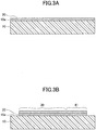
- Figs. 3A to 3C are diagrams illustrating a process of manufacturing the strain gauge according to the first embodiment, and each illustrate a cross section corresponding to Fig. 2 .
- the substrate 10 is prepared and the functional layer 20 is formed on the upper surface 10a of the substrate 10.
- the material and thickness for each of the substrate 10 and the functional layer 20 are the same as the material and thickness described above.
- the functional layer 20 can be vacuum-deposited by, for example, conventional sputtering in which a raw material capable of forming the functional layer 20 is the target and in which an Ar (argon) gas is supplied to a chamber.
- Ar argon
- the functional layer 20 is deposited while the upper surface 10a of the substrate 10 is etched with Ar.
- a deposited amount of film of the functional layer 20 is minimized and thus an effect of improving adhesion can be obtained.
- the functional layer 20 may be formed by other methods.
- the upper surface 10a of the substrate 10 is activated by plasma treatment using Ar, etc. or the like to thereby obtain the effect of improving the adhesion; subsequently, the functional layer 20 may be vacuum-deposited by magnetron sputtering.
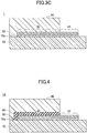
- the resistor 30 and the terminal sections 41 are formed on the entire upper surface of the functional layer 20, and then the functional layer 20, the resistor 30, and the terminal sections 41 are each patterned in the planar shape as illustrated in Fig. 1 , by photolithography.
- the material and thickness for each of the resistor 30 and the terminal sections 41 are the same as the material and thickness described above.
- the resistor 30 and the terminal sections 41 can be integrally formed of the same material.
- the resistor 30 and the terminal sections 41 can be deposited by, for example, magnetron sputtering in which a raw material capable of forming the resistor 30 and the terminal sections 41 is a target. Instead of the magnetron sputtering, the resistor 30 and the terminal sections 41 may be deposited by reactive sputtering, vapor deposition, arc ion plating, pulsed laser deposition, or the like.
- a combination of the material of the functional layer 20 and the material of the resistor 30 and the terminal sections 41 is not particularly restricted, and can be appropriately selected for any purpose.
- Ti is used for the functional layer 20, and a Cr composite film formed with ⁇ -Cr (alpha-chromium) as the main component can be deposited as the resistor 30 and the terminal sections 41.
- each of the resistor 30 and the terminal sections 41 can be deposited by, for example, magnetron sputtering in which a raw material capable of forming the Cr composite film is the target and in which an Ar gas is supplied to a chamber.
- the resistor 30 and the terminal sections 41 may be deposited by reactive sputtering in which pure Cr is the target and in which an appropriate amount of nitrogen gas, as well as an Ar gas, are supplied to a chamber.
- a growth face of the Cr composite film is defined by the functional layer 20 formed of Ti, and a Cr composite film that is formed with ⁇ -Cr as the main component having a stable crystalline structure can be deposited. Also, Ti that constitutes the functional layer 20 is diffused into the Cr composite film, so that the gauge characteristics are improved.
- the gauge factor of the strain gauge 1 can be 10 or more, as well as the gauge factor temperature coefficient TCS and temperature coefficient of resistance TCR can be each in the range of from -1000 ppm/° C to +1000 ppm/° C.
- the functional layer 20 formed of Ti includes all functions being a function of promoting crystal growth of the resistor 30; a function of preventing oxidation of the resistor 30 caused by oxygen or moisture contained in the substrate 10; and a function of improving adhesion between the substrate 10 and the resistor 30.
- the functional layer 20 is formed of Ta, Si, Al, or Fe, the functional layer also includes the same functions.
- the cover layer 60 is formed on and above the upper surface 10a of the substrate 10, such that the resistor 30 is coated and the terminal sections 41 are exposed.
- the material and thickness of the cover layer 60 are the same as the material and thickness described above.
- the cover layer 60 can be fabricated, such that a thermosetting insulating resin film in a semi-cured state is laminated on the upper surface 10a of the substrate 10, and such that the resistor 30 is coated and the terminal sections 41 are exposed; subsequently, heat is added and curing is performed.
- the cover layer 60 may be formed, such that a thermosetting insulating resin that is liquid or paste-like is applied to the upper surface 10a of the substrate 10, and such that the resistor 30 is coated and the terminal sections 41 are exposed; subsequently, heat is added and curing is performed. In the above process, the strain gauge 1 is completed.
- the crystal growth of the resistor 30 can be promoted and thus the resistor 30 having a stable crystalline phase can be fabricated.
- the stability of the gauge characteristics can be improved.
- the material that constitutes the functional layer 20 is diffused into the resistor 30, so that the gauge characteristics of the strain gauge 1 can be thereby improved.
- Modification 1 of the first embodiment provides an example of a strain gauge in which an insulating layer is provided in a lower layer of the cover layer. Note that in the modification 1 of the first embodiment, the explanation for the same components as the embodiment that has been described may be omitted.
- Fig. 4 is a cross-sectional view illustrating an example of the strain gauge according to the modification 1 of the first embodiment, and illustrates a cross section corresponding to Fig. 2 .
- the strain gauge 1A differs from the strain gauge 1 (see Figs. 1 and 2 , etc.) in that an insulating layer 50 is provided in the lower layer of the cover layer 60.
- the cover layer 60 may be provided to cover all portions except for the terminal sections 41.
- the insulating layer 50 is provided on and above the upper surface 10a of the substrate 10, such that the resistor 30 is coated and the terminal sections 41 are exposed.
- the cover layer 60 can be provided to cover a portion of a side surface of the insulating layer 50, and an upper surface thereof.
- the material of the insulating layer 50 is not particularly restricted as long as the material has higher resistance than the resistor 30 and the cover layer 60.
- the material can be appropriately selected for any purpose.
- an oxide or a nitride, such as Si, W, Ti, or Ta, can be used.
- the thickness of the insulating layer 50 is not particularly restricted, and can be appropriately selected for any purpose. For example, the thickness can be approximately between 0.05 ⁇ m and 1 ⁇ m.
- the method of forming the insulating layer 50 is not particularly restricted, and can be appropriately selected for any purpose.
- a vacuum process such as sputtering or chemical vapor deposition (CVD), or, a solution process such as spin coating or a sol-gel process can be used.
- the insulating layer 50 being provided in the lower layer of the cover layer 60, insulation and environmental sealing can be improved in comparison to the case where the cover layer 60 alone is used. In such a manner, the insulating layer 50 can be appropriately provided according to a specification required for the insulation and environmental sealing.
- the second embodiment provides an example of a strain gauge in which each electrode has a laminated structure. Note that in the second embodiment, the explanation for the same components as the embodiment that has been described may be omitted.
- Fig. 5 is a plan view illustrating an example of a strain gauge according to the second embodiment.
- Fig. 6 is a cross-sectional view illustrating an example of the strain gauge according to the second embodiment, and illustrates a cross section taken along the line B-B in Fig. 5 .
- the strain gauge 2 includes electrodes 40A in each of which a plurality of layers are laminated. Note that the cover layer 60 may be provided to cover all portions except for the electrodes 40A.
- Each electrode 40A has a laminated structure in which a plurality of metallic layers are laminated. Specifically, each electrode 40A includes a terminal section 41 extending from a corresponding end portion from among both end portions of the resistor 30; a metallic layer 42 formed on an upper surface of the terminal section 41; a metallic layer 43 formed on an upper surface of the metallic layer 42; and a metallic layer 44 formed on an upper surface of the metallic layer 43.
- the metallic layer 43 is a typical example of a first metallic layer according to the present invention
- the metallic layer 44 is a typical example of a second metallic layer according to the present invention.
- the material of the metallic layer 42 is not particularly restricted, and can be appropriately selected for any purpose.
- Cu copper
- the thickness of the metallic layer 42 is not particularly restricted, and can be appropriately selected for any purpose.
- the thickness can be approximately in the range of from 0.01 ⁇ m to 1 ⁇ m.
- the material of the metallic layer 43 includes Cu, a Cu alloy, Ni, or a Ni alloy.
- the thickness of the metallic layer 43 is determined in consideration of solderability to the electrode 40A, and is preferably 1 ⁇ m or more, and more preferably 3 ⁇ m or more.
- the material of the metallic layer 43 includes Cu, a Cu alloy, Ni, or a Ni alloy and the thickness of the metallic layer 43 is 1 ⁇ m or more, dissolution of metallization is ameliorated.
- the material of the metallic layer 43 includes Cu, a Cu alloy, Ni, or a Ni alloy and the thickness of the metallic layer 43 is 3 ⁇ m or more, dissolution of metallization is further ameliorated.
- the thickness of the metallic layer 43 is preferably 30 ⁇ m or less in terms of ease of electrolytic plating.
- the dissolution of metallization means that the material constituting the electrode 40A is dissolved in solder for jointing the electrode 40A, and that the thickness of the electrode 40A is reduced or the material disappears.
- adhesion strength or tensile strength with a lead wire, or the like to be jointed to the electrode 40A may be reduced.
- the material of the metallic layer 44 material having better solder wettability than the metallic layer 43 can be selected.
- the material of the metallic layer 44 can include Au (gold).
- Au gold
- the surface of Cu, a Cu alloy, Ni, or a Ni alloy is coated with Au, oxidation and corrosion for Cu, a Cu alloy, Ni, or a Ni alloy can be prevented, as well as good solder wettability can be provided.
- the material of the metallic layer 44 includes Pt (platinum), the metallic layer 44 has the same effect.
- the thickness of the metallic layer 44 is not particularly restricted, and can be appropriately selected for any purpose. For example, the thickness can be approximately between 0.01 ⁇ m and 1 ⁇ m.
- each terminal section 41 is exposed around a given laminated section of the metallic layers 42, 43, and 44, in a plan view.
- each terminal section 41 may have the same planar shape as the laminated section of the metallic layers 42, 43, and 44.
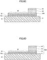
- Figs. 7A to 8D illustrate a process of manufacturing a strain gauge according to a second embodiment, and illustrate a cross section corresponding to Fig. 6 .
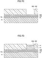
- a process that is similar to that in Fig. 3A according to the first embodiment is first performed, and then in the process illustrated in Fig. 7A , a metallic layer 300 is formed on an upper surface of the functional layer 20.
- the metallic layer 300 is a layer that is finally patterned to serve as the resistor 30 and terminal sections 41.
- the material and thickness of the metallic layer 300 are the same as the material and thickness for each of the above resistor 30 and terminal sections 41.
- the metallic layer 300 can be deposited by magnetron sputtering in which, for example, a raw material capable of forming the metallic layer 300 is the target. Instead of the magnetron sputtering, the metallic layer 300 may be deposited by reactive sputtering, vapor deposition, arc ion plating, pulsed laser deposition, or the like.
- a seed layer 420 as the metallic layer 42 is formed by, for example, sputtering, electroless plating, or the like, to cover an upper surface of the metallic layer 300.
- a photosensitive resist 800 is formed on the entire upper surface of the seed layer 420, and by exposing and developing, an opening 800x for exposing a region in which each electrode 40A is to be formed is formed.
- the resist 800 for example, a dry film resist, or the like can be used.
- a given metallic layer 43 is formed on the seed layer 420 that is exposed in the opening 800x, by for example, electrolytic plating in which the seed layer 420 is set as a power supply path, and further, a given metallic layer 44 is formed on the metallic layer 43.
- the electrolytic plating is suitable because it has high takt and allows for formation of a low stress electrolytic plating layer as the metallic layer 43.
- the metallic layer 44 may be formed on the metallic layer 43, by electroless plating.
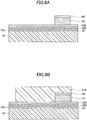
- the resist 800 illustrated in Fig. 7D is removed.
- the resist 800 can be removed by, for example, immersing the material of the resist 800 in a dissolvable solution.
- a photosensitive resist 810 is formed on the entire upper surface of the seed layer 420, and by exposing and developing, a planar shape that is the same as that of the resistor 30 and terminal sections 41 in Fig. 5 is patterned.
- the resist 810 for example, a dry film resist, or the like can be used.
- the resist 810 is used as an etch mask, and the functional layer 20, the metallic layer 300, and the seed layer 420 that are exposed from the resist 810 are removed, so that the functional layer 20, the resistor 30, and the terminal sections 41 each of which has the planar shape in Fig. 5 are formed.
- the functional layer 20; the metallic layer 300; and the seed layer 420 can be removed. Note that at this point, the seed layer 420 is formed on the resistor 30.
- the metallic layer 43 and the metallic layer 44 are used as etch masks, and an unwanted seed layer 420 that is exposed from the metallic layer 43 and the metallic layer 44 is removed, so that the metallic layer 42 is formed.
- the unwanted seed layer 420 can be removed.
- the cover layer 60 with which the resistor 30 is coated and that exposes the electrodes 40A is formed on and above the upper surface 10a of the substrate 10, so that the strain gauge 2 is completed.
- each electrode 40A As described above, as each electrode 40A, a given metallic layer 43 formed of a thick film (1 ⁇ m or more), which is formed of Cu, a Cu alloy, Ni, or a Ni alloy, is formed above a given terminal section 41, and further, a given metallic layer 44 formed of material (Au or Pt) that has better solder wettability than the metallic layer 43 is formed in the outermost surface layer. Thereby, dissolution of metallization can be prevented, as well as improving solder wettability.
- Modification 1 of the second embodiment provides an example of electrodes each having a layer structure different from that in the second embodiment. Note that in the modification 1 of the second embodiment, the explanation for the same components as the embodiments that have been described may be omitted.
- Fig. 9 is a cross-sectional view illustrating an example of a strain gauge according to the modification 1 of the second embodiment, and illustrates a cross section corresponding to Fig. 6 .
- the strain gauge 2A differs from the strain gauge 2 (see Fig. 6 , etc.) in that the electrodes 40A are replaced with electrodes 40B.
- the cover layer 60 is provided to approximately cover all portions except for the electrodes 40B, which differs from the strain gauge 2 (see Fig. 6 , etc.).
- Each electrode 40B has a laminated structure in which a plurality of metallic layers are laminated.
- each electrode 40B includes a terminal section 41 extending from a corresponding end portion from among both end portions of the resistor 30; a metallic layer 42 formed on an upper surface of the terminal section 41; a metallic layer 43 formed on an upper surface of the metallic layer 42; a metallic layer 45 formed on an upper surface of the metallic layer 43; and a metallic layer 44 formed on an upper surface of the metallic layer 45.
- each electrode 40B has a structure in which the metallic layer 45 is provided between the metallic layer 43 and the metallic layer 44 of a given electrode 40A.
- the material of the metallic layer 45 is not particularly restricted, and can be appropriately selected for any purpose.
- Ni can be used.
- NiP nickel phosphorus
- Pd nickel phosphorus
- the metallic layer 45 Ni/Pd (a metallic layer in which a Ni layer and a Pd layer are laminated in this order) may be used.
- the thickness of the metallic layer 45 is not particularly restricted, and can be appropriately selected for any purpose. For example, the thickness is approximately between 1 ⁇ m and 2 ⁇ m.
- the metallic layer 45 can be formed on the metallic layer 43 by, for example, electrolytic plating in which the seed layer 420 is set as a power supply path.
- the number of electrode layers is not particularly restricted, and the number of layers may be increased as necessary.
- a given metallic layer 43 formed of a thick film (1 ⁇ m or more), which is formed of Cu, a Cu alloy, Ni, or a Ni alloy, is formed above a given terminal section 41, and further, a given metallic layer 44 formed of material (Au or Pt) that has better solder wettability than the metallic layer 43 is formed in the outermost surface layer.
- Modification 2 of the second embodiment provides another example of electrodes each having a different layer structure from that in the second embodiment. Note that in the modification 2 of the second embodiment, the explanation for the same components as the embodiments that have been described may be omitted.
- Fig. 10 is a cross-sectional view illustrating an example of a strain gauge according to the modification 2 of the second embodiment, and illustrates a cross section corresponding to Fig. 6 .
- the strain gauge 2B differs from the strain gauge 2A (see Fig. 9 ) in that the electrodes 40B are replaced with electrodes 40C.
- the cover layer 60 is provided to approximately cover all portions except for the electrodes 40C, which differs from the strain gauge 2 (see Fig. 6 , etc.).
- Each electrode 40C has a laminated structure in which a plurality of metallic layers are laminated.
- each electrode 40C includes a terminal section 41 extending from a corresponding end portion from among both end portions of the resistor 30; a metallic layer 42 formed on an upper surface of the terminal section 41; a metallic layer 43 formed on an upper surface of the metallic layer 42; a metallic layer 45A formed on an upper surface and side surfaces of the metallic layer 43 and on side surfaces of the metallic layer 42; and a metallic layer 44A formed on an upper surface and side surfaces of the metallic layer 45A.
- the material and thickness for each of the metallic layers 44A and 45A can be the same as the material and thickness of the metallic layers 44 and 45.
- the metallic layer 44A is a typical example of a second metallic layer according to the present invention.
- each electrode 40C In order to form each electrode 40C, first, in the process illustrated in Fig. 7D , for example, a given metallic layer 43 is formed by, for example, electrolytic plating in which the seed layer 420 is set as a power supply path, and then the resist 800 is removed as is the case with the process illustrated in Fig. 8A , without forming a given metallic layer 44. Next, the same process as that in Figs. 8B to 8D is performed. Subsequently, a given metallic layer 45A can be formed on the upper surface and side surfaces of the metallic layer 43 and on the side surfaces of the metallic layer 42, by electroless plating, for example. Additionally, a given metallic layer 44A can be formed on the upper surface and side surfaces of the metallic layer 45A, by electroless plating, for example.
- each electrode can be fabricated by appropriately using both of electrolytic plating and electroless plating.
- the metallic layer 44A of the outermost layer is formed, via the metallic layer 45A, toward the side surfaces of each of the metallic layers 42 and 43, in addition to the upper surface of the metallic layer 43.
- the effect of preventing oxidation and corrosion of Cu, a Cu alloy, Ni, or a Ni alloy that constitutes the metallic layer 43 can be further enhanced, as well as the solder wettability can be further improved.
- the same effect is obtained even when a given metallic layer 44A is formed directly on the upper surface and side surfaces of a given metallic layer 43 and on the side surfaces of a given metallic layer 42, without forming a given metallic layer 45A.
- the metallic layer 44A may directly or indirectly cover the upper surface and side surfaces of the metallic layer 43 and the side surfaces of the metallic layer 42.
- a third embodiment provides an example of a sensor module using a strain gauge. Note that in the third embodiment, the explanation for the same components as the embodiments that have been described may be omitted.
- Fig. 11 is a cross-sectional view illustrating an example of the sensor module according to the third embodiment, and illustrates a cross section corresponding to Fig. 2 .
- the sensor module 5 includes the strain gauge 1, a flexure element 110, and an adhesive layer 120.
- the cover layer 60 may be provided to cover all portions except for the terminal sections 41.
- an upper surface 110a of the flexure element 110 is secured to the lower surface 10b of the substrate 10, via the adhesive layer 120.
- the flexure element 110 is an object that is formed of a metal such as Fe, SUS (stainless steel), or Al, or, a resin such as PEEK, and that is deformed (causes strain) according to force that is applied.
- the strain gauge 1 can detect strain generated in the flexure element 110, as a change in a resistance value of the resistor 30.
- the material of the adhesive layer 120 is not particularly restricted as long as it has a function of securing the flexure element 110 to the strain gauge 1.
- the material can be appropriately selected for any purpose.
- an epoxy resin, a modified epoxy resin, a silicone resin, a modified silicone resin, a urethane resin, a modified urethane resin, or the like can be used.
- material such as a bonding sheet may be used.
- the thickness of the adhesive layer 120 is not particularly restricted, and can be appropriately selected for any purpose. For example, the thickness can be approximately between 0.1 ⁇ m and 50 ⁇ m.
- any material described above, which constitutes the adhesive layer 120 is applied to the lower surface 10b of the substrate 10 and/or the upper surface 110a of the flexure element 110. Then, the lower surface 10b of the substrate 10 is situated facing the upper surface 110a of the flexure element 110, and the strain gauge 1 is disposed above the flexure element 110, through the applied material. Alternatively, the bonding sheet may be interposed between the flexure element 110 and the substrate 10.
- the strain gauge 1 is heated to a predetermined temperature while being pressed toward the flexure element 110, and the applied material is cured, so that the adhesive layer 120 is formed.
- the lower surface 10b of the substrate 10 is secured to the upper surface 110a of the flexure element 110, through the adhesive layer 120, so that the sensor module 5 is completed.
- the sensor module 5 can be applied in measurement of load, pressure, torque, acceleration, or the like.
- the strain gauge 1A, 2, 2A, or 2B may be used instead of the strain gauge 1.
- Ti as the functional layer 20 was vacuum-deposited on the upper surface 10a of the substrate 10 formed of a polyimide resin that had a thickness of 25 ⁇ m, by conventional sputtering.
- five samples for each of which Ti was deposited were fabricated in order to target multiple film thicknesses.
- X-ray fluorescence (XRF) analysis was performed to obtain the result as illustrated in Fig. 12 .
- XRF X-ray fluorescence
- Example 1 Ti as the functional layer 20, which had a film thickness of 3 nm, was vacuum-deposited on the upper surface 10a of the substrate 10 formed of a polyimide resin that had a thickness of 25 ⁇ m, by conventional sputtering.
- a Cr composite film as the resistor 30 and the terminal sections 41, was deposited on the entire upper surface of the functional layer 20, by magnetron sputtering, and then the functional layer 20, the resistor 30, and the terminal sections 41 were patterned by photolithography, as illustrated in Fig. 1 .
- a Cr composite film, as the resistor 30 and the terminal sections 41 was deposited on the upper surface 10a of the substrate 10 formed of a polyimide resin that had a thickness of 25 ⁇ m, by magnetron sputtering. Then, patterning was performed by photolithography, as illustrated in Fig. 1 . Note that for the sample used in Example 1 and the sample used in comparative example 1, all deposition conditions for the resistor 30 and the terminal sections 41 are the same.
- Fig. 13 illustrates an X-ray diffraction pattern at a diffraction angle of 2 ⁇ being in the range of from 36 to 48 degrees, and a diffraction peak in Example 1 is shifted to the right in comparison to a diffraction peak in comparative example 1. Further, the diffraction peak in Example 1 is greater than the diffraction peak in comparative example 1.
- Example 1 The diffraction peak in Example 1 is situated in proximity to a diffraction line of ⁇ -Cr (110). This is considered that when the functional layer 20 formed of Ti was provided, crystal growth of ⁇ -Cr was promoted to thereby form a Cr composite film with ⁇ -Cr as the main component.
- Example 1 multiple samples used in Example 1 and comparative example 1 were fabricated, and gauge characteristics were measured. As a result, a gauge factor for each sample in Example 1 was between 14 and 16. In contrast, a gauge factor for each sample in comparative example 1 was less than 10.
- the gauge factor temperature coefficient TCS and temperature coefficient of resistance TCR were each in the range of from -1000 ppm/° C to +1000 ppm/° C.
- the gauge factor temperature coefficient TCS and temperature coefficient of resistance TCR were not each in the range of from -1000 ppm/° C to +1000 ppm/° C.
- Example 2 multiple substrates 10 each formed of a polyimide resin that had a thickness of 25 ⁇ m and that had a different expansion coefficient were prepared. Then, when a Cr-composite film, as a given resistor 30, was deposited, a relationship between an expansion coefficient of a given substrate 10 and internal stress of the resistor 30 was checked, to thereby obtain the result illustrated in Fig. 14 .
- the internal stress of the resistor 30 was estimated by measuring warp in an evaluation sample and using the Stoney formula given by Formula (1). Note that as can be seen from Formula (1), the internal stress of the resistor 30 illustrated in Fig. 14 indicates a value per unit thickness and does not depend on the thickness of the resistor 30.
- E denotes Young's modulus
- ⁇ denotes Poisson's ratio
- D denotes the thickness of the substrate 10
- t denotes the thickness of the resistor 30
- R denotes change in radius of curvature in the substrate 10.
- ⁇ 0.4 GPa indicates values expressing a permittable warp in the strain gauge 1 for functioning, and was experimentally determined by the inventors.
- the expansion coefficient of the substrate 10 is required to be in the range of from 7 ppm/K to 20 ppm/K.
- the material of the substrate 10 does not necessarily include a polyimide resin.
- the expansion coefficient of the substrate 10 can be in the range of from 7 ppm/K to 20 ppm/K, by selecting the material of the substrate 10, selecting the material of the filler contained in the substrate 10, adjusting the content, and the like.
- the expansion coefficient of the substrate 10 being in the range of from 7 ppm/K to 20 ppm/K
- a difference in the expansion coefficient between the substrate 10 and the resistor 30, as well as other factors, are absorbed, so that the internal stress of the resistor 30 can be in the range of ⁇ 0.4 GPa.
- warp in the strain gauge 1 is reduced to thereby cause the strain gauge 1 to be able to function stably in a manner such that good gauge characteristics are maintained.
- Example 3 multiple substrates 10 each formed of a polyimide resin that had a thickness of 25 ⁇ m and that contained fillers were prepared. Three sets of samples, each of which included a sample not being subject to heat treatment; a sample being subject to heat treatment at a temperature of 100 °C; a sample being subject to heat treatment at a temperature of 200 °C; and a sample being subject to heat treatment at a temperature of 300 °C, were fabricated. Then, the samples were returned to be at normal temperature, and surface unevenness on the upper surface 10a of each substrate 10 was measured by three-dimensional optical interference.
- the resistor 30 having a film thickness of 0.05 ⁇ m was deposited on the upper surface 10a of each substrate 10, by magnetron sputtering, and patterning was performed by photolithography, as illustrated in Fig. 1 . Then, the number of pinholes that were generated in the resistor 30 was measured by a light transmission method in which light was transmitted from a back surface of a given sample.
- Fig. 15 a relationship between surface unevenness on the upper surface 10a of a given substrate 10 and the number of pinholes that were generated in a given resistor 30 was summarized in Fig. 15 .
- each bar graph illustrated in Fig. 15 shows surface unevenness
- a line graph shows the number of pinholes.
- 100 °C, 200 °C, and 300 °C each indicate a temperature when a given substrate 10 was subject to heat treatment, and Incomplete indicates that heat treatment is not carried out.
- Fig. 15 indicates that when a given substrate 10 is heated at temperatures between 100 °C and 300 °C, the surface unevenness on the upper surface 10a of the substrate 10 is 15 nm or less, which is about half of surface unevenness in a case of being incomplete, and that as a result, the number of pinholes in the resistor 30 is drastically reduced to about 1/7.
- the heat treatment be carried out at temperatures between 100 °C and 250 °C. Note that it is considered that the surface unevenness is reduced by heat treatment because fillers are contained in a polyimide resin that constitutes the substrate 10, during thermal shrinkage caused by the heat treatment.
- the number of pinholes (about 140) in the case of Incomplete, as illustrated in Fig. 15 indicates a level of the gauge characteristics deteriorating.
- the number of pinholes (about 20) after heat treatment indicates a level of the gauge characteristics not being adversely affected.
- the resistor 30 having a film thickness of 0.05 ⁇ m is used, in a case where the surface unevenness on the upper surface 10a of the substrate 10 is 15 nm or less, it was confirmed that the number of pinholes that were generated in the resistor 30 could be reduced to indicate a level of the gauge characteristics not being adversely affected.
- the resistor 30 having a film thickness of greater than 0.05 ⁇ m when the surface unevenness on the upper surface 10a of the substrate 10 is 15 nm or less, the number of pinholes that are generated in the resistor 30 can be reduced to indicate a level of the gauge characteristics not being adversely affected.
- the resistor 30 having a film thickness of 0.05 ⁇ m or more when the resistor 30 having a film thickness of 0.05 ⁇ m or more is used, the number of pinholes that are generated in the resistor 30 can be reduced to indicate a level of the gauge characteristics not being adversely affected.
- the surface unevenness on the upper surface 10a of the substrate 10 can be 15 nm or less, and as a result, the number of pinholes that are generated in the resistor 30 having a film thickness of 0.05 ⁇ m or more can be significantly reduced. As a result, the strain gauge 1 can function stably in a manner such that good gauge characteristics are maintained.
- the surface unevenness on the upper surface 10a of the substrate 10 can be reduced by, for example, a method of scraping a protrusion by approximately vertically irradiating the upper surface 10a of the substrate 10, with laser light; a method of cutting a protrusion by moving a water cutter or the like to be parallel to the upper surface 10a of the substrate 10; a method of polishing the upper surface 10a of the substrate 10 with a grinding wheel; a method of pressing the substrate 10 while heating (heat press); or the like.
- the surface unevenness on the upper surface 10a of the substrate 10 is not necessarily limited to being directed to surface unevenness caused by the fillers that are present. It is effective to reduce surface unevenness not being caused by the fillers that are present, by various methods described above. For example, when surface unevenness on the substrate 10 without containing fillers is greater than 15 nm, in a case where the surface unevenness on the upper surface 10a of the substrate 10 is 15 nm or less, by various methods described above, the number of pinholes that are generated in the resistor 30 having a film thickness of 0.05 ⁇ m or more can be reduced to a level of the gauge characteristics not being adversely affected.
- Example 4 the process illustrated in Figs. 7A to 8D was modified as described in the modification 1 of the second embodiment, the strain gauge 2A with the electrodes 40B was fabricated, and the presence or absence of dissolution of metallization was checked. Specifically, 10 types of samples in each of which Cu was used for the metallic layers 42 and 43, in each of which NiP was used for the metallic layer 45, in each of which Au was used for the metallic layer 44, and in each of which the thickness of a given metallic layer was changed were fabricated (samples No. 1 to No. 10), and then the presence or absence of dissolution of metallization was checked.
- Table 1 shows results. Note that in Table 1, the film thickness "0" indicates that no metallic layer was formed. The “poor” indicates that dissolution of metallization occurred in soldering being first performed. The “good” indicates that although no dissolution of metallization occurred in soldering being first performed, little dissolution of metallization occurred in soldering being performed second (where soldering refinement, etc. was assumed). Additionally, the “excellent” indicates that dissolution of metallization occurred neither in soldering being performed first nor second. [Table 1] SAMPLE No.
Landscapes
- Physics & Mathematics (AREA)
- General Physics & Mathematics (AREA)
- Engineering & Computer Science (AREA)
- Microelectronics & Electronic Packaging (AREA)
- Chemical & Material Sciences (AREA)
- Materials Engineering (AREA)
- Mechanical Engineering (AREA)
- Metallurgy (AREA)
- Organic Chemistry (AREA)
- Manufacturing & Machinery (AREA)
- Measurement Of Length, Angles, Or The Like Using Electric Or Magnetic Means (AREA)
Abstract
Description
- The present invention relates to a strain gauge and a sensor module.
- A strain gauge is known to be attached to a measured object to detect strain on the measured object. The strain gauge includes a resistor that detects strain, and as resistor material, for example, material including Cr (chromium) or Ni (nickel) is used. The resistor is formed on a substrate made of, for example, an insulating resin (see, for example, Patent document 1).
- [Patent document 1] Japanese Unexamined Patent Application Publication No.
2016-74934 - However, when a flexible substrate is used, a stable resistor is not easily formed on the substrate, and thus there is a problem in instability of gauge characteristics (a gauge factor, a gauge factor temperature coefficient TCS, and a temperature coefficient of resistance TCR).
- In view of the point described above, an object of the present invention is to improve stability of gauge characteristics of a strain gauge including a resistor formed above a flexible substrate.
- A strain gauge includes a flexible substrate; a functional layer formed of a metal, an alloy, or a metal compound, on one surface of the substrate; a resistor formed of material including at least one from among chromium and nickel, on one surface of the functional layer; and an insulating resin layer with which the resistor is coated.
- According to the disclosed technique, with respect to a strain gauge including a resistor formed above a flexible substrate, stability of gauge characteristics can be improved.
-
- [
Fig. 1 ]
Fig. 1 is a plan view of an example of a strain gauge according to a first embodiment; - [
Fig. 2 ]
Fig. 2 is a cross-sectional view of an example of the strain gauge according to the first embodiment; - [
Fig. 3A ]
Fig. 3A is a diagram (part 1) illustrating an example of a process of manufacturing the strain gauge according to the first embodiment; - [
Fig. 3B ]
Fig. 3B is a diagram (part 2) illustrating an example of the process of manufacturing the strain gauge according to the first embodiment; - [
Fig. 3C ]
Fig. 3C is a diagram (part 3) illustrating an example of the process of manufacturing the strain gauge according to the first embodiment; - [
Fig. 4 ]
Fig. 4 is a cross-sectional view of an example of a strain gauge according tomodification 1 of the first embodiment; - [
Fig. 5 ]
Fig. 5 is a plan view of an example of a strain gauge according to a second embodiment; - [
Fig. 6 ]
Fig. 6 is a cross-sectional view of an example of the strain gauge according to the second embodiment; - [
Fig. 7A ]
Fig. 7A is a diagram (part 1) illustrating an example of a process of manufacturing the strain gauge according to the second embodiment; - [
Fig. 7B ]
Fig. 7B is a diagram (part 2) illustrating an example of the process of manufacturing the strain gauge according to the second embodiment; - [
Fig. 7C ]
Fig. 7C is a diagram (part 3) illustrating an example of the process of manufacturing the strain gauge according to the second embodiment; - [
Fig. 7D ]
Fig. 7D is a diagram (part 4) illustrating an example of the process of manufacturing the strain gauge according to the second embodiment; - [
Fig. 8A ]
Fig. 8A is a diagram (part 5) illustrating an example of the process of manufacturing the strain gauge according to the second embodiment; - [
Fig. 8B ]
Fig. 8B is a diagram (part 6) illustrating an example of the process of manufacturing the strain gauge according to the second embodiment; - [
Fig. 8C ]
Fig. 8C is a diagram (part 7) illustrating an example of the process of manufacturing the strain gauge according to the second embodiment; - [
Fig. 8D ]
Fig. 8D is a diagram (part 8) illustrating an example of the process of manufacturing the strain gauge according to the second embodiment; - [
Fig. 9 ]
Fig. 9 is a cross-sectional view of an example of a strain gauge according tomodification 1 of the second embodiment; - [
Fig. 10 ]
Fig. 10 is a cross-sectional view of an example of a strain gauge according tomodification 2 of the second embodiment; - [
Fig. 11 ]
Fig. 11 is a cross-sectional view of an example of a sensor module according to a third embodiment; - [
Fig. 12 ]
Fig. 12 is a diagram illustrating a result of X-ray fluorescent analysis for a functional layer; - [
Fig. 13 ]
Fig. 13 is a diagram illustrating a result of X-ray diffraction for a resistor; - [
Fig. 14 ]
Fig. 14 is a diagram illustrating a relationship between an expansion coefficient of a substrate and internal stress of a resistor; and - [
Fig. 15 ]
Fig. 15 is a diagram illustrating a relationship between surface unevenness of a substrate and the number of pinholes of a resistor. - One or more embodiments will be hereinafter described with reference to the drawings. In each figure, the same numerals denote the same components; accordingly, duplicative explanations may be omitted.
-
Fig. 1 is a plan view of an example of a strain gauge according to a first embodiment.Fig. 2 is a cross-sectional view of an example of the strain gauge according to the first embodiment, and illustrates a cross section taken along the A-A line inFig. 1 . With reference toFigs. 1 and 2 , thestrain gauge 1 includes asubstrate 10, afunctional layer 20, aresistor 30,terminal sections 41, and acover layer 60. Note that inFig. 1 , an outer edge of thecover layer 60 is only expressed by a dashed line in order to indicate theresistor 30, for the sake of convenience. - Note that in the present embodiment, for the sake of convenience, with respect to the
strain gauge 1, the side of thesubstrate 10 where theresistor 30 is provided is referred to as an upper side or one side; and the side of thesubstrate 10 where theresistor 30 is not provided is referred to as a lower side or another side. Further, for each component, the surface on the side where theresistor 30 is provided is referred to as one surface or an upper surface; and the surface on the side where theresistor 30 is not provided is referred to as another surface or a lower surface. However, thestrain gauge 1 can be used in a state of being upside down, or be disposed at any angle. Further, a plan view means that an object is viewed from a normal direction of anupper surface 10a of thesubstrate 10, and a planar shape refers to a shape of an object when viewed from the normal direction of theupper surface 10a of thesubstrate 10. - The
substrate 10 is a member that is a base layer for forming theresistor 30 or the like and is flexible. The thickness of thesubstrate 10 is not particularly restricted, and can be appropriately selected for any purpose. For example, such a thickness can be approximately between 5 µm and 500 µm. In particular, when the thickness of thesubstrate 10 is between 5 µm and 200 µm, it is preferable in terms of strain transfer from a flexure element surface that is bonded to a lower surface of thesubstrate 10 via an adhesive layer or the like; and dimensional stability with respect to environment, and when the thickness is 10 µm or more, it is further preferable in terms of insulation. - The
substrate 10 can be formed of an insulating resin film such as a PI (polyimide) resin, an epoxy resin, a PEEK (polyether ether ketone) resin, a PEN (polyethylene naphthalate) resin, a PET (polyethylene terephthalate) resin, a PPS (polyphenylene sulfide) resin, or a polyolefin resin. Note that the film refers to a flexible member having a thickness of about 500 µm or less. - Here, the "formed of an insulating resin film" is not intended to preclude the
substrate 10 from containing fillers, impurities, or the like in the insulating resin film. Thesubstrate 10 may be formed of, for example, an insulating resin film containing fillers such as silica or alumina. - The
functional layer 20 is formed, as a lower layer of theresistor 30, on theupper surface 10a of thesubstrate 10. In other words, a planar shape of thefunctional layer 20 is approximately the same as the planar shape of theresistor 30 illustrated inFig. 1 . The thickness of thefunctional layer 20 can be approximately between 1 nm and 100 nm, for example. - In the present application, the functional layer refers to a layer that has a function of promoting crystal growth of the
resistor 30 that is at least an upper layer. Thefunctional layer 20 preferably further has a function of preventing oxidation of theresistor 30 caused by oxygen and moisture included in thesubstrate 10, as well as a function of improving adhesion between thesubstrate 10 and theresistor 30. Thefunctional layer 20 may further have other functions. - The insulating resin film that constitutes the
substrate 10 contains oxygen and moisture. In this regard, particularly when theresistor 30 includes Cr (chromium), it is effective for thefunctional layer 20 to have a function of preventing oxidation of theresistor 30, because Cr forms an autoxidized film. - The material of the
functional layer 20 is not particularly restricted as long as it is material having a function of promoting crystal growth of theresistor 30 that is at least an upper layer. Such material can be appropriately selected for any purpose, and includes one or more types of metals selected from a group consisting of, for example, Cr (chromium), Ti (titanium), V (vanadium), Nb (niobium), Ta (tantalum), Ni (nickel), Y (yttrium), Zr (zirconium), Hf (hafnium), Si (silicon), C (carbon), Zn (zinc), Cu (copper), Bi (bismuth), Fe (iron), Mo (molybdenum), W (tungsten), Ru (ruthenium), Rh (rhodium), Re (rhenium), Os (osmium), Ir (iridium), Pt (platinum), Pd (palladium), Ag (silver), Au (gold), Co (cobalt), Mn (manganese), and Al (aluminum); an alloy of any metals from among the group; or a compound of any metal from among the group. - Examples of the above alloy include FeCr, TiAl, FeNi, NiCr, CrCu, and the like. Examples of the above compound include TiN, TaN, Si3N4, TiO2, Ta2O5, SiO2, and the like.
- The
resistor 30 is a thin film formed in a predetermined pattern and above the upper surface of thefunctional layer 20, and is a sensitive section where resistance varies according to strain. Note that inFig. 1 , for the sake of convenience, theresistor 30 is illustrated in a crepe pattern. - The
resistor 30 can be formed of, for example, material including Cr (chromium); material including Ni (nickel); or material including both of Cr and Ni. In other words, theresistor 30 can be formed of material including at least one from among Cr and Ni. An example of the material including Cr includes a Cr composite film. An example of the material including nickel includes Cu-Ni (copper nickel). An example of the material including both of Cr and Ni includes Ni-Cr (nickel chromium). - Here, the Cr composite film is a composite film of Cr, CrN, Cr2N, and the like. The Cr composite film may include incidental impurities such as chromium oxide. A portion of the material that constitutes the
functional layer 20 may also be diffused into the Cr composite film. In this case, the material that constitutes thefunctional layer 20, and nitrogen may form a compound. For example, when thefunctional layer 20 is formed of Ti, the Cr composite film may include Ti or TiN (titanium nitride). - The thickness of the
resistor 30 is not particularly restricted, and can be appropriately selected for any purpose. The thickness can be, for example, approximately between 0.05 µm and 2 µm. In particular, when the thickness of theresistor 30 is 0.1 µm or more, it is preferable in terms of improvement in crystallinity (e.g., crystallinity of α-Cr) of a crystal that constitutes theresistor 30, and when the thickness of theresistor 30 is 1 µm or less, it is further preferable in terms of reduction in cracks of a given film caused by internal stress of the film that constitutes theresistor 30, or reduction in warp in thesubstrate 10. - With the
resistor 30 being formed on thefunctional layer 20, theresistor 30 can be formed by a stable crystalline phase and thus stability of gauge characteristics (a gauge factor, a gauge factor temperature coefficient TCS, and a temperature coefficient of resistance TCR) can be improved. - For example, when the
resistor 30 is the Cr composite film, in a case of providing thefunctional layer 20, theresistor 30 can be formed with α-Cr (alpha-chromium) as the main component. Because α-Cr has a stable crystalline phase, the stability of the gauge characteristics can be improved. - Here, a main component means that a target substance has 50% by weight or more of total substances that constitute the resistor. When the
resistor 30 is the Cr composite film, theresistor 30 preferably includes α-Cr of 80% by weight or more, from the viewpoint of improving the gauge characteristics. Note that α-Cr is Cr having a bcc structure (body-centered cubic structure). - Also, by diffusing a metal (e.g., Ti) that constitutes the
functional layer 20 into the Cr composite film, the gauge characteristics can be improved. Specifically, the gauge factor of thestrain gauge 1 can be 10 or more, as well as the gauge factor temperature coefficient TCS and temperature coefficient of resistance TCR can be each in the range of from -1000 ppm/°C to +1000 ppm/°C. - Note that the expansion coefficient of the
substrate 10 is preferably between 7 ppm/K and 20 ppm/K, from the viewpoint of reducing warp in thesubstrate 10, where the internal stress of theresistor 30 is assumed to be close to zero. The expansion coefficient of thesubstrate 10 can be adjusted by, for example, selecting the material of thesubstrate 10, selecting the material of the filler contained in thesubstrate 10, adjusting the content, and the like. - When the
resistor 30 is formed above thesubstrate 10, pinholes may be generated in theresistor 30. If the number of pinholes generated in theresistor 30 exceeds a predetermined value, the gauge characteristics might deteriorate, or the resistor might not serve as a strain gauge. The inventors have recognized that one of causes of a pinhole being generated in theresistor 30 relates to filler protruding from theupper surface 10a of thesubstrate 10. - In other words, when the
substrate 10 includes a filler, a portion of the filler protrudes from theupper surface 10a of thesubstrate 10, so that surface unevenness on theupper surface 10a of thesubstrate 10 increases. As a result, the number of pinholes that are generated in theresistor 30 formed above theupper surface 10a of thesubstrate 10 increases, which results in deterioration of the gauge characteristics, and the like. - The inventors have found that, when the thickness of the
resistor 30 is 0.05 µm or more, in a case where the surface unevenness on theupper surface 10a of thesubstrate 10 is 15 nm or less, the number of pinholes that are generated in theresistor 30 can be suppressed to maintain the gauge characteristics. - In other words, when the thickness of the
resistor 30 is 0.05 µm or more, the surface unevenness on theupper surface 10a of thesubstrate 10 is preferably 15 nm or less, from the viewpoint of reducing the number of pinholes that are generated in theresistor 30 formed above theupper surface 10a of thesubstrate 10 to maintain the gauge characteristics. When the surface unevenness is 15 nm or less, even in a case where thesubstrate 10 includes fillers, the gauge characteristics do not deteriorate. Note that the surface unevenness on theupper surface 10a of thesubstrate 10 may be 0 nm. - The surface unevenness on the
upper surface 10a of thesubstrate 10 can be reduced by, for example, heating thesubstrate 10. Alternatively, instead of heating of thesubstrate 10, a method of scraping a protrusion by approximately vertically irradiating theupper surface 10a of thesubstrate 10 with laser light; a method of cutting a protrusion by moving a water cutter or the like to be parallel to theupper surface 10a of thesubstrate 10; a method of polishing theupper surface 10a of thesubstrate 10 with a grinding wheel; a method of pressing thesubstrate 10 while heating (heat press); or the like, may be used. - Note that the surface unevenness means arithmetical mean roughness, and is generally expressed by Ra. The surface unevenness can be measured by, for example, three-dimensional optical interferometry.
- The
terminal sections 41 respectively extend from both end portions of theresistor 30 and are each wider than theresistor 30 to be in an approximately rectangular shape, in a plan view. Theterminal sections 41 are a pair of electrodes from which a change in a resistance value of theresistor 30 according to strain is output externally, where, for example, a lead wire for an external connection, or the like is joined. For example, theresistor 30 extends zigzagged back and forth from one of theterminal sections 41 to anotherterminal section 41. The upper surface of eachterminal section 41 may be coated with a metal allowing for better solderability than theterminal section 41. Note that for the sake of convenience, theresistor 30 and theterminal sections 41 are expressed by different numerals. However, the resistor and the terminal sections can be integrally formed of the same material, in the same process. - The
cover layer 60 is an insulating resin layer, which is disposed on and above theupper surface 10a of thesubstrate 10, such that theresistor 30 is coated and theterminal sections 41 are exposed. With thecover layer 60 being provided, mechanical damage, and the like can be prevented from occurring in theresistor 30. Additionally, with thecover layer 60 being provided, theresistor 30 can be protected against moisture, and the like. Note that thecover layer 60 may be provided to cover the entire portion except for theterminal sections 41. - The
cover layer 60 can be formed of an insulating resin such as a PI resin, an epoxy resin, a PEEK resin, a PEN resin, a PET resin, or a PPS resin, a composite resin (e.g., a silicone resin or a polyolefin resin). Thecover layer 60 may contain fillers or pigments. The thickness of thecover layer 60 is not particularly restricted, and can be appropriately selected for any purpose. For example, the thickness may be approximately between 2 µm and 30 µm. -
Figs. 3A to 3C are diagrams illustrating a process of manufacturing the strain gauge according to the first embodiment, and each illustrate a cross section corresponding toFig. 2 . In order to manufacture thestrain gauge 1, first, in the process illustrated inFig. 3A , thesubstrate 10 is prepared and thefunctional layer 20 is formed on theupper surface 10a of thesubstrate 10. The material and thickness for each of thesubstrate 10 and thefunctional layer 20 are the same as the material and thickness described above. - The
functional layer 20 can be vacuum-deposited by, for example, conventional sputtering in which a raw material capable of forming thefunctional layer 20 is the target and in which an Ar (argon) gas is supplied to a chamber. By using conventional sputtering, thefunctional layer 20 is deposited while theupper surface 10a of thesubstrate 10 is etched with Ar. Thus, a deposited amount of film of thefunctional layer 20 is minimized and thus an effect of improving adhesion can be obtained. - However, this is an example of a method of depositing the
functional layer 20, and thefunctional layer 20 may be formed by other methods. For example, before depositing thefunctional layer 20, theupper surface 10a of thesubstrate 10 is activated by plasma treatment using Ar, etc. or the like to thereby obtain the effect of improving the adhesion; subsequently, thefunctional layer 20 may be vacuum-deposited by magnetron sputtering. - Next, in the process illustrated in
Fig. 3B , theresistor 30 and theterminal sections 41 are formed on the entire upper surface of thefunctional layer 20, and then thefunctional layer 20, theresistor 30, and theterminal sections 41 are each patterned in the planar shape as illustrated inFig. 1 , by photolithography. The material and thickness for each of theresistor 30 and theterminal sections 41 are the same as the material and thickness described above. Theresistor 30 and theterminal sections 41 can be integrally formed of the same material. Theresistor 30 and theterminal sections 41 can be deposited by, for example, magnetron sputtering in which a raw material capable of forming theresistor 30 and theterminal sections 41 is a target. Instead of the magnetron sputtering, theresistor 30 and theterminal sections 41 may be deposited by reactive sputtering, vapor deposition, arc ion plating, pulsed laser deposition, or the like. - A combination of the material of the
functional layer 20 and the material of theresistor 30 and theterminal sections 41 is not particularly restricted, and can be appropriately selected for any purpose. For example, Ti is used for thefunctional layer 20, and a Cr composite film formed with α-Cr (alpha-chromium) as the main component can be deposited as theresistor 30 and theterminal sections 41. - In this case, each of the
resistor 30 and theterminal sections 41 can be deposited by, for example, magnetron sputtering in which a raw material capable of forming the Cr composite film is the target and in which an Ar gas is supplied to a chamber. Alternatively, theresistor 30 and theterminal sections 41 may be deposited by reactive sputtering in which pure Cr is the target and in which an appropriate amount of nitrogen gas, as well as an Ar gas, are supplied to a chamber. - In such methods, a growth face of the Cr composite film is defined by the
functional layer 20 formed of Ti, and a Cr composite film that is formed with α-Cr as the main component having a stable crystalline structure can be deposited. Also, Ti that constitutes thefunctional layer 20 is diffused into the Cr composite film, so that the gauge characteristics are improved. For example, the gauge factor of thestrain gauge 1 can be 10 or more, as well as the gauge factor temperature coefficient TCS and temperature coefficient of resistance TCR can be each in the range of from -1000 ppm/° C to +1000 ppm/° C. - Note that when the
resistor 30 is a Cr composite film, thefunctional layer 20 formed of Ti includes all functions being a function of promoting crystal growth of theresistor 30; a function of preventing oxidation of theresistor 30 caused by oxygen or moisture contained in thesubstrate 10; and a function of improving adhesion between thesubstrate 10 and theresistor 30. Instead of Ti, when thefunctional layer 20 is formed of Ta, Si, Al, or Fe, the functional layer also includes the same functions. - Next, in the process illustrated in
Fig. 3C , thecover layer 60 is formed on and above theupper surface 10a of thesubstrate 10, such that theresistor 30 is coated and theterminal sections 41 are exposed. The material and thickness of thecover layer 60 are the same as the material and thickness described above. For example, thecover layer 60 can be fabricated, such that a thermosetting insulating resin film in a semi-cured state is laminated on theupper surface 10a of thesubstrate 10, and such that theresistor 30 is coated and theterminal sections 41 are exposed; subsequently, heat is added and curing is performed. Thecover layer 60 may be formed, such that a thermosetting insulating resin that is liquid or paste-like is applied to theupper surface 10a of thesubstrate 10, and such that theresistor 30 is coated and theterminal sections 41 are exposed; subsequently, heat is added and curing is performed. In the above process, thestrain gauge 1 is completed. - As described above, with the
functional layer 20 being provided in the lower layer of theresistor 30, the crystal growth of theresistor 30 can be promoted and thus theresistor 30 having a stable crystalline phase can be fabricated. As a result, with respect to thestrain gauge 1, the stability of the gauge characteristics can be improved. Also, the material that constitutes thefunctional layer 20 is diffused into theresistor 30, so that the gauge characteristics of thestrain gauge 1 can be thereby improved. -
Modification 1 of the first embodiment provides an example of a strain gauge in which an insulating layer is provided in a lower layer of the cover layer. Note that in themodification 1 of the first embodiment, the explanation for the same components as the embodiment that has been described may be omitted. -
Fig. 4 is a cross-sectional view illustrating an example of the strain gauge according to themodification 1 of the first embodiment, and illustrates a cross section corresponding toFig. 2 . With reference toFig. 4 , thestrain gauge 1A differs from the strain gauge 1 (seeFigs. 1 and 2 , etc.) in that an insulatinglayer 50 is provided in the lower layer of thecover layer 60. Note that thecover layer 60 may be provided to cover all portions except for theterminal sections 41. - The insulating
layer 50 is provided on and above theupper surface 10a of thesubstrate 10, such that theresistor 30 is coated and theterminal sections 41 are exposed. For example, thecover layer 60 can be provided to cover a portion of a side surface of the insulatinglayer 50, and an upper surface thereof. - The material of the insulating
layer 50 is not particularly restricted as long as the material has higher resistance than theresistor 30 and thecover layer 60. The material can be appropriately selected for any purpose. For example, an oxide or a nitride, such as Si, W, Ti, or Ta, can be used. The thickness of the insulatinglayer 50 is not particularly restricted, and can be appropriately selected for any purpose. For example, the thickness can be approximately between 0.05 µm and 1 µm. - The method of forming the insulating
layer 50 is not particularly restricted, and can be appropriately selected for any purpose. For example, a vacuum process such as sputtering or chemical vapor deposition (CVD), or, a solution process such as spin coating or a sol-gel process can be used. - In such a manner, with the insulating
layer 50 being provided in the lower layer of thecover layer 60, insulation and environmental sealing can be improved in comparison to the case where thecover layer 60 alone is used. In such a manner, the insulatinglayer 50 can be appropriately provided according to a specification required for the insulation and environmental sealing. - The second embodiment provides an example of a strain gauge in which each electrode has a laminated structure. Note that in the second embodiment, the explanation for the same components as the embodiment that has been described may be omitted.
-
Fig. 5 is a plan view illustrating an example of a strain gauge according to the second embodiment.Fig. 6 is a cross-sectional view illustrating an example of the strain gauge according to the second embodiment, and illustrates a cross section taken along the line B-B inFig. 5 . With reference toFigs. 5 and 6 , thestrain gauge 2 includeselectrodes 40A in each of which a plurality of layers are laminated. Note that thecover layer 60 may be provided to cover all portions except for theelectrodes 40A. - Each
electrode 40A has a laminated structure in which a plurality of metallic layers are laminated. Specifically, eachelectrode 40A includes aterminal section 41 extending from a corresponding end portion from among both end portions of theresistor 30; ametallic layer 42 formed on an upper surface of theterminal section 41; ametallic layer 43 formed on an upper surface of themetallic layer 42; and ametallic layer 44 formed on an upper surface of themetallic layer 43. Themetallic layer 43 is a typical example of a first metallic layer according to the present invention, and themetallic layer 44 is a typical example of a second metallic layer according to the present invention. - The material of the
metallic layer 42 is not particularly restricted, and can be appropriately selected for any purpose. For example, Cu (copper) can be used. The thickness of themetallic layer 42 is not particularly restricted, and can be appropriately selected for any purpose. For example, the thickness can be approximately in the range of from 0.01 µm to 1 µm. - Preferably, the material of the
metallic layer 43 includes Cu, a Cu alloy, Ni, or a Ni alloy. The thickness of themetallic layer 43 is determined in consideration of solderability to theelectrode 40A, and is preferably 1 µm or more, and more preferably 3 µm or more. When the material of themetallic layer 43 includes Cu, a Cu alloy, Ni, or a Ni alloy and the thickness of themetallic layer 43 is 1 µm or more, dissolution of metallization is ameliorated. Also, when the material of themetallic layer 43 includes Cu, a Cu alloy, Ni, or a Ni alloy and the thickness of themetallic layer 43 is 3 µm or more, dissolution of metallization is further ameliorated. Note that the thickness of themetallic layer 43 is preferably 30 µm or less in terms of ease of electrolytic plating. - Here, the dissolution of metallization means that the material constituting the
electrode 40A is dissolved in solder for jointing theelectrode 40A, and that the thickness of theelectrode 40A is reduced or the material disappears. When the dissolution of metallization occurs, adhesion strength or tensile strength with a lead wire, or the like to be jointed to theelectrode 40A may be reduced. Thus, it is preferable that no dissolution of metallization occur. - For the material of the
metallic layer 44, material having better solder wettability than themetallic layer 43 can be selected. For example, when the material of themetallic layer 43 includes Cu, a Cu alloy, Ni, or a Ni alloy, the material of themetallic layer 44 can include Au (gold). When the surface of Cu, a Cu alloy, Ni, or a Ni alloy is coated with Au, oxidation and corrosion for Cu, a Cu alloy, Ni, or a Ni alloy can be prevented, as well as good solder wettability can be provided. Instead of Au, when the material of themetallic layer 44 includes Pt (platinum), themetallic layer 44 has the same effect. The thickness of themetallic layer 44 is not particularly restricted, and can be appropriately selected for any purpose. For example, the thickness can be approximately between 0.01 µm and 1 µm. - Note that each
terminal section 41 is exposed around a given laminated section of themetallic layers terminal section 41 may have the same planar shape as the laminated section of themetallic layers -
Figs. 7A to 8D illustrate a process of manufacturing a strain gauge according to a second embodiment, and illustrate a cross section corresponding toFig. 6 . In order to manufacture thestrain gauge 2, a process that is similar to that inFig. 3A according to the first embodiment is first performed, and then in the process illustrated inFig. 7A , ametallic layer 300 is formed on an upper surface of thefunctional layer 20. Themetallic layer 300 is a layer that is finally patterned to serve as theresistor 30 andterminal sections 41. In such a manner, the material and thickness of themetallic layer 300 are the same as the material and thickness for each of theabove resistor 30 andterminal sections 41. - The
metallic layer 300 can be deposited by magnetron sputtering in which, for example, a raw material capable of forming themetallic layer 300 is the target. Instead of the magnetron sputtering, themetallic layer 300 may be deposited by reactive sputtering, vapor deposition, arc ion plating, pulsed laser deposition, or the like. - Next, in the process illustrated in
Fig. 7B , aseed layer 420 as themetallic layer 42 is formed by, for example, sputtering, electroless plating, or the like, to cover an upper surface of themetallic layer 300. - Next, in the process illustrated in
Fig. 7C , a photosensitive resist 800 is formed on the entire upper surface of theseed layer 420, and by exposing and developing, anopening 800x for exposing a region in which eachelectrode 40A is to be formed is formed. As the resist 800, for example, a dry film resist, or the like can be used. - Next, in the process illustrated in
Fig. 7D , a givenmetallic layer 43 is formed on theseed layer 420 that is exposed in theopening 800x, by for example, electrolytic plating in which theseed layer 420 is set as a power supply path, and further, a givenmetallic layer 44 is formed on themetallic layer 43. The electrolytic plating is suitable because it has high takt and allows for formation of a low stress electrolytic plating layer as themetallic layer 43. When the electrolytic plating layer whose thickness is increased has low stress, warp in thestrain gauge 2 can be prevented. Note that themetallic layer 44 may be formed on themetallic layer 43, by electroless plating. - Note that in forming the
metallic layer 44, side surfaces of themetallic layer 43 are coated with the resist 800, so that themetallic layer 44 is formed only on the upper surface of themetallic layer 43 and is not on the side surfaces thereof. - Next, in the process illustrated in
Fig. 8A , the resist 800 illustrated inFig. 7D is removed. The resist 800 can be removed by, for example, immersing the material of the resist 800 in a dissolvable solution. - Next, in the process illustrated in
Fig. 8B , a photosensitive resist 810 is formed on the entire upper surface of theseed layer 420, and by exposing and developing, a planar shape that is the same as that of theresistor 30 andterminal sections 41 inFig. 5 is patterned. As the resist 810, for example, a dry film resist, or the like can be used. - Next, in the process illustrated in
Fig. 8C , the resist 810 is used as an etch mask, and thefunctional layer 20, themetallic layer 300, and theseed layer 420 that are exposed from the resist 810 are removed, so that thefunctional layer 20, theresistor 30, and theterminal sections 41 each of which has the planar shape inFig. 5 are formed. For example, with wet etching, unwanted portions of thefunctional layer 20; themetallic layer 300; and theseed layer 420 can be removed. Note that at this point, theseed layer 420 is formed on theresistor 30. - Next, in the process illustrated in
Fig. 8D , themetallic layer 43 and themetallic layer 44 are used as etch masks, and anunwanted seed layer 420 that is exposed from themetallic layer 43 and themetallic layer 44 is removed, so that themetallic layer 42 is formed. For example, by wet etching using etching liquid with which theseed layer 420 is etched and with which thefunctional layer 20 and theresistor 30 are not etched, theunwanted seed layer 420 can be removed. - After the process illustrated in
Fig. 8D , as is the case with the process inFig. 3C , thecover layer 60 with which theresistor 30 is coated and that exposes theelectrodes 40A is formed on and above theupper surface 10a of thesubstrate 10, so that thestrain gauge 2 is completed. - As described above, as each
electrode 40A, a givenmetallic layer 43 formed of a thick film (1 µm or more), which is formed of Cu, a Cu alloy, Ni, or a Ni alloy, is formed above a giventerminal section 41, and further, a givenmetallic layer 44 formed of material (Au or Pt) that has better solder wettability than themetallic layer 43 is formed in the outermost surface layer. Thereby, dissolution of metallization can be prevented, as well as improving solder wettability. -
Modification 1 of the second embodiment provides an example of electrodes each having a layer structure different from that in the second embodiment. Note that in themodification 1 of the second embodiment, the explanation for the same components as the embodiments that have been described may be omitted. -
Fig. 9 is a cross-sectional view illustrating an example of a strain gauge according to themodification 1 of the second embodiment, and illustrates a cross section corresponding toFig. 6 . With reference toFig. 9 , thestrain gauge 2A differs from the strain gauge 2 (seeFig. 6 , etc.) in that theelectrodes 40A are replaced withelectrodes 40B. Additionally, thecover layer 60 is provided to approximately cover all portions except for theelectrodes 40B, which differs from the strain gauge 2 (seeFig. 6 , etc.). - Each
electrode 40B has a laminated structure in which a plurality of metallic layers are laminated. Specifically, eachelectrode 40B includes aterminal section 41 extending from a corresponding end portion from among both end portions of theresistor 30; ametallic layer 42 formed on an upper surface of theterminal section 41; ametallic layer 43 formed on an upper surface of themetallic layer 42; ametallic layer 45 formed on an upper surface of themetallic layer 43; and ametallic layer 44 formed on an upper surface of themetallic layer 45. In other words, eachelectrode 40B has a structure in which themetallic layer 45 is provided between themetallic layer 43 and themetallic layer 44 of a givenelectrode 40A. - The material of the
metallic layer 45 is not particularly restricted, and can be appropriately selected for any purpose. For example, Ni can be used. Instead of Ni, NiP (nickel phosphorus) or Pd may be used. Also, as themetallic layer 45, Ni/Pd (a metallic layer in which a Ni layer and a Pd layer are laminated in this order) may be used. The thickness of themetallic layer 45 is not particularly restricted, and can be appropriately selected for any purpose. For example, the thickness is approximately between 1 µm and 2 µm. - In the process illustrated in
Fig. 7D , themetallic layer 45 can be formed on themetallic layer 43 by, for example, electrolytic plating in which theseed layer 420 is set as a power supply path. - In such a manner, the number of electrode layers is not particularly restricted, and the number of layers may be increased as necessary. In this case as well, a given
metallic layer 43 formed of a thick film (1 µm or more), which is formed of Cu, a Cu alloy, Ni, or a Ni alloy, is formed above a giventerminal section 41, and further, a givenmetallic layer 44 formed of material (Au or Pt) that has better solder wettability than themetallic layer 43 is formed in the outermost surface layer. Thereby, as is the case with the second embodiment, the dissolution of metallization can be prevented, as well as improving the solder wettability. -
Modification 2 of the second embodiment provides another example of electrodes each having a different layer structure from that in the second embodiment. Note that in themodification 2 of the second embodiment, the explanation for the same components as the embodiments that have been described may be omitted. -
Fig. 10 is a cross-sectional view illustrating an example of a strain gauge according to themodification 2 of the second embodiment, and illustrates a cross section corresponding toFig. 6 . With reference toFig. 10 , thestrain gauge 2B differs from thestrain gauge 2A (seeFig. 9 ) in that theelectrodes 40B are replaced withelectrodes 40C. Additionally, thecover layer 60 is provided to approximately cover all portions except for theelectrodes 40C, which differs from the strain gauge 2 (seeFig. 6 , etc.). - Each
electrode 40C has a laminated structure in which a plurality of metallic layers are laminated. Specifically, eachelectrode 40C includes aterminal section 41 extending from a corresponding end portion from among both end portions of theresistor 30; ametallic layer 42 formed on an upper surface of theterminal section 41; ametallic layer 43 formed on an upper surface of themetallic layer 42; ametallic layer 45A formed on an upper surface and side surfaces of themetallic layer 43 and on side surfaces of themetallic layer 42; and ametallic layer 44A formed on an upper surface and side surfaces of themetallic layer 45A. For example, the material and thickness for each of themetallic layers metallic layers metallic layer 44A is a typical example of a second metallic layer according to the present invention. - In order to form each
electrode 40C, first, in the process illustrated inFig. 7D , for example, a givenmetallic layer 43 is formed by, for example, electrolytic plating in which theseed layer 420 is set as a power supply path, and then the resist 800 is removed as is the case with the process illustrated inFig. 8A , without forming a givenmetallic layer 44. Next, the same process as that inFigs. 8B to 8D is performed. Subsequently, a givenmetallic layer 45A can be formed on the upper surface and side surfaces of themetallic layer 43 and on the side surfaces of themetallic layer 42, by electroless plating, for example. Additionally, a givenmetallic layer 44A can be formed on the upper surface and side surfaces of themetallic layer 45A, by electroless plating, for example. - As described above, each electrode can be fabricated by appropriately using both of electrolytic plating and electroless plating. In the structure of each electrode 40C, a given
metallic layer 43 formed of a thick film (1 µm or more), which is formed of Cu, a Cu alloy, Ni, or a Ni alloy, is formed above a giventerminal section 41, and further, a givenmetallic layer 44A formed of material (Au or Pt) that has better solder wettability than themetallic layer 43 is formed in the outermost layer. Note, however, that themetallic layer 44A of the outermost layer is formed, via themetallic layer 45A, toward the side surfaces of each of themetallic layers metallic layer 43. Thus, in comparison to theelectrodes 40A or theelectrodes 40B, the effect of preventing oxidation and corrosion of Cu, a Cu alloy, Ni, or a Ni alloy that constitutes themetallic layer 43 can be further enhanced, as well as the solder wettability can be further improved. - Note that the same effect is obtained even when a given
metallic layer 44A is formed directly on the upper surface and side surfaces of a givenmetallic layer 43 and on the side surfaces of a givenmetallic layer 42, without forming a givenmetallic layer 45A. In other words, themetallic layer 44A may directly or indirectly cover the upper surface and side surfaces of themetallic layer 43 and the side surfaces of themetallic layer 42. - A third embodiment provides an example of a sensor module using a strain gauge. Note that in the third embodiment, the explanation for the same components as the embodiments that have been described may be omitted.
-
Fig. 11 is a cross-sectional view illustrating an example of the sensor module according to the third embodiment, and illustrates a cross section corresponding toFig. 2 . With reference toFig. 11 , thesensor module 5 includes thestrain gauge 1, aflexure element 110, and anadhesive layer 120. Note that thecover layer 60 may be provided to cover all portions except for theterminal sections 41. - In the
sensor module 5, anupper surface 110a of theflexure element 110 is secured to thelower surface 10b of thesubstrate 10, via theadhesive layer 120. For example, theflexure element 110 is an object that is formed of a metal such as Fe, SUS (stainless steel), or Al, or, a resin such as PEEK, and that is deformed (causes strain) according to force that is applied. Thestrain gauge 1 can detect strain generated in theflexure element 110, as a change in a resistance value of theresistor 30. - The material of the
adhesive layer 120 is not particularly restricted as long as it has a function of securing theflexure element 110 to thestrain gauge 1. The material can be appropriately selected for any purpose. For example, an epoxy resin, a modified epoxy resin, a silicone resin, a modified silicone resin, a urethane resin, a modified urethane resin, or the like can be used. Also, material such as a bonding sheet may be used. The thickness of theadhesive layer 120 is not particularly restricted, and can be appropriately selected for any purpose. For example, the thickness can be approximately between 0.1 µm and 50 µm. - In order to manufacture the
sensor module 5, after thestrain gauge 1 is fabricated, for example, any material described above, which constitutes theadhesive layer 120, is applied to thelower surface 10b of thesubstrate 10 and/or theupper surface 110a of theflexure element 110. Then, thelower surface 10b of thesubstrate 10 is situated facing theupper surface 110a of theflexure element 110, and thestrain gauge 1 is disposed above theflexure element 110, through the applied material. Alternatively, the bonding sheet may be interposed between theflexure element 110 and thesubstrate 10. - Next, the
strain gauge 1 is heated to a predetermined temperature while being pressed toward theflexure element 110, and the applied material is cured, so that theadhesive layer 120 is formed. Thereby, thelower surface 10b of thesubstrate 10 is secured to theupper surface 110a of theflexure element 110, through theadhesive layer 120, so that thesensor module 5 is completed. For example, thesensor module 5 can be applied in measurement of load, pressure, torque, acceleration, or the like. - Note that for the
sensor module 5, thestrain gauge strain gauge 1. - First, in an advance test, Ti as the
functional layer 20 was vacuum-deposited on theupper surface 10a of thesubstrate 10 formed of a polyimide resin that had a thickness of 25 µm, by conventional sputtering. In this case, five samples for each of which Ti was deposited were fabricated in order to target multiple film thicknesses. - Next, for the fabricated five samples, X-ray fluorescence (XRF) analysis was performed to obtain the result as illustrated in
Fig. 12 . From an X-ray peak inFig. 12 , it was confirmed that Ti was present, and from X-ray intensity of each sample at the X-ray peak, it was confirmed that a film thickness of a given Ti film could be controlled to be in the range of from 1 nm to 100 nm. - Next, in Example 1, Ti as the
functional layer 20, which had a film thickness of 3 nm, was vacuum-deposited on theupper surface 10a of thesubstrate 10 formed of a polyimide resin that had a thickness of 25 µm, by conventional sputtering. - Subsequently, a Cr composite film, as the
resistor 30 and theterminal sections 41, was deposited on the entire upper surface of thefunctional layer 20, by magnetron sputtering, and then thefunctional layer 20, theresistor 30, and theterminal sections 41 were patterned by photolithography, as illustrated inFig. 1 . - In comparative example 1, without forming the
functional layer 20, a Cr composite film, as theresistor 30 and theterminal sections 41, was deposited on theupper surface 10a of thesubstrate 10 formed of a polyimide resin that had a thickness of 25 µm, by magnetron sputtering. Then, patterning was performed by photolithography, as illustrated inFig. 1 . Note that for the sample used in Example 1 and the sample used in comparative example 1, all deposition conditions for theresistor 30 and theterminal sections 41 are the same. - Next, for a given sample used in Example 1 and a given sample used in comparative example 1, X-ray diffraction evaluation was performed to obtain the result illustrated in
Fig. 13. Fig. 13 illustrates an X-ray diffraction pattern at a diffraction angle of 2θ being in the range of from 36 to 48 degrees, and a diffraction peak in Example 1 is shifted to the right in comparison to a diffraction peak in comparative example 1. Further, the diffraction peak in Example 1 is greater than the diffraction peak in comparative example 1. - The diffraction peak in Example 1 is situated in proximity to a diffraction line of α-Cr (110). This is considered that when the
functional layer 20 formed of Ti was provided, crystal growth of α-Cr was promoted to thereby form a Cr composite film with α-Cr as the main component. - Next, multiple samples used in Example 1 and comparative example 1 were fabricated, and gauge characteristics were measured. As a result, a gauge factor for each sample in Example 1 was between 14 and 16. In contrast, a gauge factor for each sample in comparative example 1 was less than 10.
- Also, for each sample in Example 1, the gauge factor temperature coefficient TCS and temperature coefficient of resistance TCR were each in the range of from -1000 ppm/° C to +1000 ppm/° C. In contrast, for each sample in comparative example 1, the gauge factor temperature coefficient TCS and temperature coefficient of resistance TCR were not each in the range of from -1000 ppm/° C to +1000 ppm/° C.
- As described above, with the
functional layer 20 formed of Ti being provided, crystal growth of α-Cr was promoted and a Cr composite film was formed with α-Cr as the main component, so that a strain gauge that had a gauge factor of 10 or more, and that had the gauge factor temperature coefficient TCS and temperature coefficient of resistance TCR being each in the range of from -1000 ppm/° C to +1000 ppm/° C, was fabricated. Note that the diffusion effect of Ti into the Cr composite film is considered to cause the improvement in the gauge characteristics. - In Example 2,
multiple substrates 10 each formed of a polyimide resin that had a thickness of 25 µm and that had a different expansion coefficient were prepared. Then, when a Cr-composite film, as a givenresistor 30, was deposited, a relationship between an expansion coefficient of a givensubstrate 10 and internal stress of theresistor 30 was checked, to thereby obtain the result illustrated inFig. 14 . - The internal stress of the
resistor 30 was estimated by measuring warp in an evaluation sample and using the Stoney formula given by Formula (1). Note that as can be seen from Formula (1), the internal stress of theresistor 30 illustrated inFig. 14 indicates a value per unit thickness and does not depend on the thickness of theresistor 30. -

substrate 10, t denotes the thickness of theresistor 30, and R denotes change in radius of curvature in thesubstrate 10. - From
Fig. 14 , when the expansion coefficient of thesubstrate 10 is in the range of from 7 ppm/K to 20 ppm/K, the internal stress of theresistor 30 can be maintained to be in the range of ±0.4 GPa. Where, ±0.4 GPa indicates values expressing a permittable warp in thestrain gauge 1 for functioning, and was experimentally determined by the inventors. - In other words, when the expansion coefficient of the
substrate 10 is out of the range of from 7 ppm/K to 20 ppm/K, the internal stress of theresistor 30 is out of the range of ±0.4 GPa and thus warp in thestrain gauge 1 would increase, so that thestrain gauge 1 would not function as a strain gauge. Therefore, the expansion coefficient of thesubstrate 10 is required to be in the range of from 7 ppm/K to 20 ppm/K. Note that the material of thesubstrate 10 does not necessarily include a polyimide resin. - The expansion coefficient of the
substrate 10 can be in the range of from 7 ppm/K to 20 ppm/K, by selecting the material of thesubstrate 10, selecting the material of the filler contained in thesubstrate 10, adjusting the content, and the like. - As described above, with the expansion coefficient of the
substrate 10 being in the range of from 7 ppm/K to 20 ppm/K, a difference in the expansion coefficient between thesubstrate 10 and theresistor 30, as well as other factors, are absorbed, so that the internal stress of theresistor 30 can be in the range of ±0.4 GPa. As a result, warp in thestrain gauge 1 is reduced to thereby cause thestrain gauge 1 to be able to function stably in a manner such that good gauge characteristics are maintained. - In Example 3,
multiple substrates 10 each formed of a polyimide resin that had a thickness of 25 µm and that contained fillers were prepared. Three sets of samples, each of which included a sample not being subject to heat treatment; a sample being subject to heat treatment at a temperature of 100 °C; a sample being subject to heat treatment at a temperature of 200 °C; and a sample being subject to heat treatment at a temperature of 300 °C, were fabricated. Then, the samples were returned to be at normal temperature, and surface unevenness on theupper surface 10a of eachsubstrate 10 was measured by three-dimensional optical interference. - Next, the
resistor 30 having a film thickness of 0.05 µm was deposited on theupper surface 10a of eachsubstrate 10, by magnetron sputtering, and patterning was performed by photolithography, as illustrated inFig. 1 . Then, the number of pinholes that were generated in theresistor 30 was measured by a light transmission method in which light was transmitted from a back surface of a given sample. - Next, based on a measured result, a relationship between surface unevenness on the
upper surface 10a of a givensubstrate 10 and the number of pinholes that were generated in a givenresistor 30 was summarized inFig. 15 . Note that each bar graph illustrated inFig. 15 shows surface unevenness, and a line graph shows the number of pinholes. Additionally, for the horizontal axis, 100 °C, 200 °C, and 300 °C each indicate a temperature when a givensubstrate 10 was subject to heat treatment, and Incomplete indicates that heat treatment is not carried out. -
Fig. 15 indicates that when a givensubstrate 10 is heated at temperatures between 100 °C and 300 °C, the surface unevenness on theupper surface 10a of thesubstrate 10 is 15 nm or less, which is about half of surface unevenness in a case of being incomplete, and that as a result, the number of pinholes in theresistor 30 is drastically reduced to about 1/7. Note, however, that in consideration of resistance to thermal temperature of a polyimide resin, when heat treatment is carried out at temperatures exceeding 250 °C, alteration or deterioration may occur. Accordingly, it is preferable that the heat treatment be carried out at temperatures between 100 °C and 250 °C. Note that it is considered that the surface unevenness is reduced by heat treatment because fillers are contained in a polyimide resin that constitutes thesubstrate 10, during thermal shrinkage caused by the heat treatment. - According to consideration by the inventors, the number of pinholes (about 140) in the case of Incomplete, as illustrated in
Fig. 15 , indicates a level of the gauge characteristics deteriorating. In contrast, the number of pinholes (about 20) after heat treatment, indicates a level of the gauge characteristics not being adversely affected. In other words, when theresistor 30 having a film thickness of 0.05 µm is used, in a case where the surface unevenness on theupper surface 10a of thesubstrate 10 is 15 nm or less, it was confirmed that the number of pinholes that were generated in theresistor 30 could be reduced to indicate a level of the gauge characteristics not being adversely affected. - Note that when the
resistor 30 having a film thickness of greater than 0.05 µm is used, it is obvious that when the surface unevenness on theupper surface 10a of thesubstrate 10 is 15 nm or less, the number of pinholes that are generated in theresistor 30 can be reduced to indicate a level of the gauge characteristics not being adversely affected. In other words, with the surface unevenness on theupper surface 10a of thesubstrate 10 being 15 nm or less, when theresistor 30 having a film thickness of 0.05 µm or more is used, the number of pinholes that are generated in theresistor 30 can be reduced to indicate a level of the gauge characteristics not being adversely affected. - As described above, with the
substrate 10 being subject to heat treatment, the surface unevenness on theupper surface 10a of thesubstrate 10 can be 15 nm or less, and as a result, the number of pinholes that are generated in theresistor 30 having a film thickness of 0.05 µm or more can be significantly reduced. As a result, thestrain gauge 1 can function stably in a manner such that good gauge characteristics are maintained. - Note that in order to reduce the number of pinholes that are generated in the
resistor 30, it is important to reduce the surface unevenness on theupper surface 10a of thesubstrate 10, and a method of reducing surface unevenness is not important. In the above description, the method of reducing surface unevenness by heat treatment has been described, but is not limited to this case. Any method may be used as long as the surface unevenness on theupper surface 10a of thesubstrate 10 can be reduced. - The surface unevenness on the
upper surface 10a of thesubstrate 10 can be reduced by, for example, a method of scraping a protrusion by approximately vertically irradiating theupper surface 10a of thesubstrate 10, with laser light; a method of cutting a protrusion by moving a water cutter or the like to be parallel to theupper surface 10a of thesubstrate 10; a method of polishing theupper surface 10a of thesubstrate 10 with a grinding wheel; a method of pressing thesubstrate 10 while heating (heat press); or the like. - Further, in order to reduce the number of pinholes that are generated in the
resistor 30, it is important to reduce the surface unevenness on theupper surface 10a of thesubstrate 10, and is not necessarily limited to being directed to surface unevenness caused by the fillers that are present. It is effective to reduce surface unevenness not being caused by the fillers that are present, by various methods described above. For example, when surface unevenness on thesubstrate 10 without containing fillers is greater than 15 nm, in a case where the surface unevenness on theupper surface 10a of thesubstrate 10 is 15 nm or less, by various methods described above, the number of pinholes that are generated in theresistor 30 having a film thickness of 0.05 µm or more can be reduced to a level of the gauge characteristics not being adversely affected. - In Example 4, the process illustrated in
Figs. 7A to 8D was modified as described in themodification 1 of the second embodiment, thestrain gauge 2A with theelectrodes 40B was fabricated, and the presence or absence of dissolution of metallization was checked. Specifically, 10 types of samples in each of which Cu was used for themetallic layers metallic layer 45, in each of which Au was used for themetallic layer 44, and in each of which the thickness of a given metallic layer was changed were fabricated (samples No. 1 to No. 10), and then the presence or absence of dissolution of metallization was checked. - Table 1 shows results. Note that in Table 1, the film thickness "0" indicates that no metallic layer was formed. The "poor" indicates that dissolution of metallization occurred in soldering being first performed. The "good" indicates that although no dissolution of metallization occurred in soldering being first performed, little dissolution of metallization occurred in soldering being performed second (where soldering refinement, etc. was assumed). Additionally, the "excellent" indicates that dissolution of metallization occurred neither in soldering being performed first nor second.
[Table 1] SAMPLE No. EACH FILM THICKNESS [µm] SOLDERABILITY Cu NiP Au 1 0.5 0 0 POOR PRESENCE OF DISSOLUTION OF METALLIZATION 2 0.5 0 0.1 POOR PRESENCE OF DISSOLUTION OF METALLIZATION 3 0.5 0 0.8 POOR PRESENCE OF DISSOLUTION OF METALLIZATION 4 1 1 0.1 GOOD ABSENCE OF DISSOLUTION OF METALLIZATION 5 3 0 0 EXCELLENT ABSENCE OF DISSOLUTION OF METALLIZATION 6 3 0 0.1 EXCELLENT ABSENCE OF DISSOLUTION OF METALLIZATION 7 3 0 0.8 EXCELLENT ABSENCE OF DISSOLUTION OF METALLIZATION 8 3 1 0.1 EXCELLENT ABSENCE OF DISSOLUTION OF METALLIZATION 9 5 1 0.1 EXCELLENT ABSENCE OF DISSOLUTION OF METALLIZATION 10 8 1 0.1 EXCELLENT ABSENCE OF DISSOLUTION OF METALLIZATION - As shown in Table 1, it was confirmed that when the thickness of Cu was 1 µm or more, dissolution of metallization was improved, and that when the thickness was 3 µm or more, the dissolution of metallization was further improved. Additionally, from the results for
sample 1 andsample 5, it was confirmed that the presence or absence of dissolution of metallization was determined only according to the thickness of Cu and was not determined upon the presence or absence of each of NiP and Au. Note, however, that as described above, in order to prevent dissolution of metallization and improve solder wettability, a metallic layer formed of Au or an equivalent material (Pt, etc.) is required. - The preferred embodiments and the like have been described above in detail, but are not limited thereto. Various modifications and alternatives to the above embodiments and the like can be made without departing from a scope set forth in the claims.
- This International application claims priority to Japanese Patent Application Nos.
2017-191824, filed September 29, 2017 2018-052422, filed March 20, 2018 - 1, 1A, 2, 2A, 2B strain gauge, 5 sensor module, 10 substrate, 10a upper surface, 20 functional layer, 30 resistor, 41 terminal section, 40A, 40B, 40C electrode, 42, 43, 44, 44A, 45, 45A metallic layer, 50 insulating layer, 60 cover layer, 110 flexure element, 120 adhesive layer
Claims (13)
- A strain gauge comprising:a flexible substrate;a functional layer formed of a metal, an alloy, or a metal compound, on one surface of the substrate;a resistor formed of material including at least one from among chromium and nickel, on one surface of the functional layer; andan insulating resin layer with which the resistor is coated.
- The strain gauge according to claim 1, wherein the functional layer includes a function of promoting crystal growth of the resistor.
- The strain gauge according to claim 1 or 2, wherein the substrate has an expansion coefficient in a range of from 7 ppm/K to 20 ppm/K.
- The strain gauge according to any one of claims 1 to 3, wherein surface unevenness on the one surface of the substrate is 15 nm or less, and
wherein the resistor has a film thickness of 0.05 µm or more. - The strain gauge according to any one of claims 1 to 4, further comprising electrodes electrically coupled to the resistor,
wherein each electrode includes:a terminal section extending from a corresponding end portion from among end portions of the resistor;a first metallic layer formed of copper, a copper alloy, nickel, or a nickel alloy, on or above the terminal section; anda second metallic layer formed of material having better solder wettability than the first metallic layer, on or above the first metallic layer. - The strain gauge according to any one of claims 1 to 5, further comprising an insulating layer which is formed, in a lower layer of the insulating resin layer, of material having higher resistance than the resistor and the insulating resin layer, and with which the resistor is coated.
- The strain gauge according to any one of claims 1 to 6, wherein a main component of the resistor is alpha-chromium.
- The strain gauge according to claim 7, wherein the resistor includes alpha-chromium of 80% by weight or more.
- The strain gauge according to claim 7 or 8, wherein the resistor includes chromium nitride.
- The strain gauge according to claim 9, wherein the functional layer includes titanium.
- The strain gauge according to claim 10, wherein the resistor includes titanium.
- The strain gauge according to claim 10 or 11, wherein the resistor includes titanium nitride.
- A sensor module comprising:the strain gauge according to any one of claims 1 to 12; anda flexure element disposed on another surface of the substrate.
Applications Claiming Priority (3)
| Application Number | Priority Date | Filing Date | Title |
|---|---|---|---|
| JP2017191824 | 2017-09-29 | ||
| JP2018052422A JP2019066454A (en) | 2017-09-29 | 2018-03-20 | Strain gauge and sensor module |
| PCT/JP2018/035727 WO2019065752A1 (en) | 2017-09-29 | 2018-09-26 | Strain gauge and sensor module |
Publications (3)
| Publication Number | Publication Date |
|---|---|
| EP3690385A1 true EP3690385A1 (en) | 2020-08-05 |
| EP3690385A4 EP3690385A4 (en) | 2021-07-07 |
| EP3690385B1 EP3690385B1 (en) | 2024-01-17 |
Family
ID=65902925
Family Applications (1)
| Application Number | Title | Priority Date | Filing Date |
|---|---|---|---|
| EP18860610.7A Active EP3690385B1 (en) | 2017-09-29 | 2018-09-26 | Strain gauge and sensor module |
Country Status (5)
| Country | Link |
|---|---|
| US (1) | US11692806B2 (en) |
| EP (1) | EP3690385B1 (en) |
| JP (3) | JP2019066454A (en) |
| CN (1) | CN111417830B (en) |
| WO (1) | WO2019065752A1 (en) |
Cited By (7)
| Publication number | Priority date | Publication date | Assignee | Title |
|---|---|---|---|---|
| US11543309B2 (en) | 2017-12-22 | 2023-01-03 | Minebea Mitsumi Inc. | Strain gauge and sensor module |
| US11543308B2 (en) | 2017-09-29 | 2023-01-03 | Minebea Mitsumi Inc. | Strain gauge |
| US11542590B2 (en) | 2017-09-29 | 2023-01-03 | Minebea Mitsumi Inc. | Strain gauge |
| US11692806B2 (en) | 2017-09-29 | 2023-07-04 | Minebea Mitsumi Inc. | Strain gauge with improved stability |
| US11747225B2 (en) | 2018-04-05 | 2023-09-05 | Minebea Mitsumi Inc. | Strain gauge with improved stability and stress reduction |
| US11774303B2 (en) | 2018-10-23 | 2023-10-03 | Minebea Mitsumi Inc. | Accelerator, steering wheel, six-axis sensor, engine, bumper and the like |
| US12411000B2 (en) | 2020-03-30 | 2025-09-09 | Minebea Mitsumi Inc. | Strain gauge |
Families Citing this family (17)
| Publication number | Priority date | Publication date | Assignee | Title |
|---|---|---|---|---|
| JP2019066313A (en) * | 2017-09-29 | 2019-04-25 | ミネベアミツミ株式会社 | Strain gauge |
| JP2019066312A (en) | 2017-09-29 | 2019-04-25 | ミネベアミツミ株式会社 | Strain gauge |
| JP2019078726A (en) * | 2017-10-27 | 2019-05-23 | ミネベアミツミ株式会社 | Strain gauge and sensor module |
| JP2019090723A (en) * | 2017-11-15 | 2019-06-13 | ミネベアミツミ株式会社 | Strain gauge |
| JP2019090722A (en) * | 2017-11-15 | 2019-06-13 | ミネベアミツミ株式会社 | Strain gauge |
| JP2019219312A (en) * | 2018-06-21 | 2019-12-26 | ミネベアミツミ株式会社 | Strain gauge |
| JP7426794B2 (en) * | 2019-10-01 | 2024-02-02 | ミネベアミツミ株式会社 | sensor module |
| JP7406517B2 (en) * | 2020-03-24 | 2023-12-27 | ミネベアミツミ株式会社 | strain gauge |
| IL275618A (en) * | 2020-06-23 | 2022-01-01 | Vishay Advanced Tech Ltd | Method of manufacture of a strain gage or flexible olyimide-based resistor |
| JP7736429B2 (en) * | 2020-10-30 | 2025-09-09 | 日東電工株式会社 | Laminated film, method for manufacturing second laminated film, and method for manufacturing strain sensor |
| CN112432720B (en) * | 2020-11-09 | 2022-08-05 | 浙江工业大学 | Load sensor element for use in a humid water environment |
| JP2022106507A (en) | 2021-01-07 | 2022-07-20 | ミネベアミツミ株式会社 | Strain gauge |
| JP7189240B2 (en) * | 2021-01-18 | 2022-12-13 | ミネベアミツミ株式会社 | strain gauge |
| JP7652502B2 (en) | 2021-05-17 | 2025-03-27 | ミネベアミツミ株式会社 | Sensor modules, battery packs |
| JP2023067057A (en) * | 2021-10-29 | 2023-05-16 | ミネベアミツミ株式会社 | strain gauge module |
| CN115323337B (en) * | 2022-10-11 | 2023-01-10 | 松诺盟科技有限公司 | Nano-film composite strain sensor and preparation method and application thereof |
| US12601645B2 (en) | 2023-07-18 | 2026-04-14 | Vishay Advanced Technologies, Ltd. | Self-adhesive strain gauge assembly including flexible printed circuit board |
Family Cites Families (124)
| Publication number | Priority date | Publication date | Assignee | Title |
|---|---|---|---|---|
| US3867231A (en) | 1972-06-28 | 1975-02-18 | Goodyear Tire & Rubber | Tire building machine |
| JPS5897607A (en) | 1981-12-07 | 1983-06-10 | Kyowa Dengiyou:Kk | Strain gauge |
| JPS58169150A (en) | 1982-03-30 | 1983-10-05 | Fujitsu Ltd | Manufacture of photomask |
| JPS59164214A (en) | 1983-03-09 | 1984-09-17 | Nissan Motor Co Ltd | Suspension device for car |
| JPS6058578U (en) | 1983-09-30 | 1985-04-23 | 日産自動車株式会社 | Braking state detection device |
| JPS60104554U (en) | 1983-12-22 | 1985-07-17 | アルパイン株式会社 | door unlocking device |
| DE3403042A1 (en) | 1984-01-30 | 1985-08-01 | Philips Patentverwaltung Gmbh, 2000 Hamburg | THIN FILM STRETCH MEASUREMENT STRIP SYSTEM AND METHOD FOR THE PRODUCTION THEREOF |
| US4658233A (en) | 1984-03-16 | 1987-04-14 | Fuji Electric Corporate Research & Development Ltd. | Strain gauge |
| DE3429649A1 (en) * | 1984-08-11 | 1986-02-20 | Vdo Adolf Schindling Ag, 6000 Frankfurt | ELECTRICAL RESISTANCE |
| JPS61176803A (en) * | 1985-01-31 | 1986-08-08 | Hitachi Ltd | strain gauge |
| JPS61288401A (en) | 1985-06-14 | 1986-12-18 | 株式会社村田製作所 | Thin film resistor |
| JPS63165725A (en) * | 1986-12-26 | 1988-07-09 | Aisin Seiki Co Ltd | Strain gauge for pressure sensor |
| US4937550A (en) * | 1987-03-31 | 1990-06-26 | Kanegafuchi Kagaku Kogyo Kabushiki Kaisha | Strain sensor |
| JP2516964B2 (en) * | 1987-03-31 | 1996-07-24 | 鐘淵化学工業株式会社 | Strain sensor |
| JPH0731091B2 (en) | 1987-05-27 | 1995-04-10 | 日本碍子株式会社 | Distortion detector |
| JP2585681B2 (en) | 1988-02-08 | 1997-02-26 | 株式会社タイセー | Metal thin film resistive strain gauge |
| JPH02117476A (en) | 1988-10-25 | 1990-05-01 | Daikyo Webasto Co Ltd | Movable rear spoiler for vehicle |
| JPH02189981A (en) | 1989-01-19 | 1990-07-25 | Ricoh Co Ltd | Semiconductor device and manufacture thereof |
| JPH0495738A (en) * | 1990-08-06 | 1992-03-27 | Teraoka Seiko Co Ltd | Load cell |
| US5154247A (en) * | 1989-10-31 | 1992-10-13 | Teraoka Seiko Co., Limited | Load cell |
| JPH03191802A (en) | 1989-12-21 | 1991-08-21 | Sumitomo Electric Ind Ltd | strain sensitive element |
| JP2890601B2 (en) | 1990-02-08 | 1999-05-17 | 株式会社デンソー | Semiconductor sensor |
| WO1991017415A1 (en) | 1990-05-07 | 1991-11-14 | Robert Bosch Gmbh | Process and device for the manufacture of a pressure force sensor |
| JPH0438402A (en) * | 1990-06-02 | 1992-02-07 | Kyowa Electron Instr Co Ltd | Strain gage and its manufacture |
| EP0460249B1 (en) | 1990-06-05 | 1994-07-27 | Hottinger Baldwin Messtechnik Gmbh | Strain gauge |
| JPH05308107A (en) | 1991-07-01 | 1993-11-19 | Sumitomo Electric Ind Ltd | Semiconductor device and its manufacture |
| JPH0580070A (en) * | 1991-09-24 | 1993-03-30 | Aisin Seiki Co Ltd | Strain gauge element and manufacture thereof |
| JPH05145142A (en) | 1991-11-19 | 1993-06-11 | Matsushita Electric Ind Co Ltd | Magnetoresistive element |
| JPH0640305A (en) | 1992-07-23 | 1994-02-15 | Toyota Motor Corp | Air bag pressure adjusting device |
| US5328551A (en) | 1992-10-28 | 1994-07-12 | Eaton Corporation | Method of making high output strain gage |
| JPH06176903A (en) | 1992-12-03 | 1994-06-24 | Nippon Soken Inc | Electrode structure of Cr-based cermet thin film |
| JPH06300649A (en) * | 1993-04-12 | 1994-10-28 | Sumitomo Electric Ind Ltd | Thin film strain resistance material, fabrication thereof and thin film strain sensor |
| JPH07113697A (en) | 1993-10-19 | 1995-05-02 | Tec Corp | Load cell |
| JP3233248B2 (en) * | 1994-05-13 | 2001-11-26 | エヌオーケー株式会社 | Thin film for strain gauge and its manufacturing method |
| JPH08102163A (en) * | 1994-09-30 | 1996-04-16 | Fujitsu Ltd | Magnetic recording medium and magnetic disk device |
| EP0725392A1 (en) | 1995-01-31 | 1996-08-07 | Hoya Corporation | Magnetic recording medium and method for fabricating the same |
| JPH08304200A (en) | 1995-05-09 | 1996-11-22 | Matsushita Electric Ind Co Ltd | Strain-sensitive resistor paste and mechanical sensor using the same |
| JPH09197435A (en) | 1996-01-17 | 1997-07-31 | Toshiba Corp | Liquid crystal display device and manufacturing method thereof |
| JP3642449B2 (en) | 1997-03-21 | 2005-04-27 | 財団法人電気磁気材料研究所 | Cr-N-based strain resistance film, manufacturing method thereof, and strain sensor |
| JP2000146511A (en) | 1998-11-06 | 2000-05-26 | Mitsubishi Heavy Ind Ltd | Strain gauge |
| JP2000207102A (en) | 1999-01-18 | 2000-07-28 | Alps Electric Co Ltd | Keyboard device |
| US6614342B1 (en) | 1999-07-09 | 2003-09-02 | Nok Corporation | Strain gauge |
| JP2002221453A (en) * | 2001-01-29 | 2002-08-09 | Nippon Denshi Kogyo Kk | System for collecting load information of structure |
| JP4482250B2 (en) | 2001-07-19 | 2010-06-16 | 本田技研工業株式会社 | Strain gauge with reduced pressure sensitivity and temperature sensitivity and design method thereof |
| US20030016116A1 (en) | 2001-07-23 | 2003-01-23 | Blaha Charles A. | Method of depositing a thin metallic film and related apparatus |
| JP2003097906A (en) | 2001-09-27 | 2003-04-03 | Tokyo Sokki Kenkyusho Co Ltd | Strain gauge and method for measuring strain |
| JP2003324258A (en) | 2002-05-01 | 2003-11-14 | Nippon Mektron Ltd | Copper-clad board for printed wiring board |
| JP2004072715A (en) | 2002-06-11 | 2004-03-04 | Murata Mfg Co Ltd | Piezoelectric thin film resonator, piezoelectric filter, and electronic part having the same |
| CN1300806C (en) | 2002-06-06 | 2007-02-14 | 阿尔卑斯电气株式会社 | Resistance element and method for manufacturing same |
| US7106167B2 (en) | 2002-06-28 | 2006-09-12 | Heetronix | Stable high temperature sensor system with tungsten on AlN |
| EP2865784A1 (en) * | 2002-08-08 | 2015-04-29 | Kabushiki Kaisha Kobe Seiko Sho (Kobe Steel, Ltd.) | Process for producing alumina coating composed mainly of alpha-type crystal structure |
| US20040159162A1 (en) | 2003-02-19 | 2004-08-19 | Vishay Intertechnology | Strain gage |
| JP2005132216A (en) | 2003-10-30 | 2005-05-26 | Matsushita Electric Ind Co Ltd | Pedal force sensor and pedal force detection device using it |
| DE502004010000D1 (en) | 2004-01-27 | 2009-10-15 | Mettler Toledo Ag | Load cells with strain gauges with inorganic-organic hybrid polymer (ORMOCER) adhesive layer |
| JP2005233953A (en) * | 2004-02-17 | 2005-09-02 | Robert Bosch Gmbh | Method for manufacturing micromechanical high pressure sensor and macromechanical pressure sensor |
| JP2006118982A (en) | 2004-10-21 | 2006-05-11 | Denso Corp | Vehicle front collision load detection device |
| JP4742577B2 (en) | 2004-12-14 | 2011-08-10 | 日産自動車株式会社 | Pressure sensor and manufacturing method thereof |
| KR20080067328A (en) | 2005-09-06 | 2008-07-18 | 비욘드 블라데스 리미티드 | 3DMC Architecture |
| JP4814594B2 (en) | 2005-09-14 | 2011-11-16 | 日立オートモティブシステムズ株式会社 | In-vehicle equipment operation device |
| DE102005052087A1 (en) * | 2005-10-28 | 2007-05-03 | Kmw Kaufbeurer Mikrosysteme Wiedemann Gmbh | sensor |
| JP4909583B2 (en) | 2005-12-16 | 2012-04-04 | 株式会社昭和測器 | Multi-axis load cell |
| JP2007173544A (en) * | 2005-12-22 | 2007-07-05 | Toshiba Corp | X-ray detector and manufacturing method thereof |
| EP2080685B1 (en) | 2008-01-16 | 2011-04-27 | Ford Global Technologies, LLC | Rotational torque sensing by means of integrated strain gauge |
| JP2010070850A (en) | 2008-08-21 | 2010-04-02 | Mitsubishi Materials Corp | Copper-clad laminate, method for manufacturing the same, printed circuit board and method for manufacturing the same |
| JP5279426B2 (en) | 2008-09-19 | 2013-09-04 | ミサワホーム株式会社 | Door lock system |
| JP2011103327A (en) | 2009-11-10 | 2011-05-26 | Seiko Epson Corp | Piezoelectric element, piezoelectric actuator, liquid injection head, and liquid injection device |
| JP2011240794A (en) | 2010-05-18 | 2011-12-01 | Takashi Aono | Vehicle recognition sound generating device |
| WO2011156447A1 (en) | 2010-06-11 | 2011-12-15 | 3M Innovative Properties Company | Positional touch sensor with force measurement |
| US8232026B2 (en) | 2010-10-14 | 2012-07-31 | Ford Global Technologies, Llc | Bipolar plates for electrochemical cells |
| JP2012151338A (en) | 2011-01-20 | 2012-08-09 | Elpida Memory Inc | Manufacturing method of semiconductor device and formation method of hard mask |
| JP5884110B2 (en) | 2011-12-02 | 2016-03-15 | 株式会社アサヒ電子研究所 | Strain resistance element and strain detection apparatus using the same |
| TWI476969B (en) | 2012-01-13 | 2015-03-11 | Univ Nat Kaohsiung Applied Sci | Metal silicide thermal sensor and its preparation method |
| JP5539430B2 (en) | 2012-03-22 | 2014-07-02 | 富士フイルム株式会社 | Manufacturing method of electronic equipment |
| JP2013217763A (en) | 2012-04-09 | 2013-10-24 | Honda Motor Co Ltd | Material for thin film strain sensor and thin film strain sensor using the same |
| JP5670502B2 (en) | 2012-04-30 | 2015-02-18 | 株式会社エスアンドエス テック | Phase reversal blank mask and manufacturing method thereof |
| CN104350366A (en) | 2012-05-25 | 2015-02-11 | 株式会社日立制作所 | Mechanical-quantity measuring device |
| CN103580980B (en) | 2012-07-24 | 2019-05-24 | 中兴通讯股份有限公司 | Method and device for automatic discovery and automatic configuration of virtual network |
| JP6022881B2 (en) * | 2012-10-04 | 2016-11-09 | 公益財団法人電磁材料研究所 | Strain gauge |
| US9306207B2 (en) | 2012-12-28 | 2016-04-05 | Hyundai Motor Company | Method of fabricating sulfur-infiltrated mesoporous conductive nanocomposites for cathode of lithium-sulfur secondary battery |
| JP6075114B2 (en) | 2013-02-27 | 2017-02-08 | ローム株式会社 | Semiconductor device and manufacturing method of semiconductor device |
| US9469107B2 (en) | 2013-07-12 | 2016-10-18 | Hewlett-Packard Development Company, L.P. | Thermal inkjet printhead stack with amorphous metal resistor |
| JP6159613B2 (en) * | 2013-08-05 | 2017-07-05 | 公益財団法人電磁材料研究所 | Strain sensor |
| US20150296607A1 (en) | 2014-04-11 | 2015-10-15 | Apple Inc. | Electronic Device With Flexible Printed Circuit Strain Gauge Sensor |
| EP3153833B1 (en) | 2014-06-09 | 2020-10-21 | Hitachi Automotive Systems, Ltd. | Dynamic quantity measuring device and pressure sensor using same |
| JP6276658B2 (en) | 2014-07-09 | 2018-02-07 | 新光電気工業株式会社 | Substrate with film thickness measuring function and method for measuring film thickness of insulating layer |
| JP6162670B2 (en) | 2014-10-03 | 2017-07-12 | 株式会社東京測器研究所 | Strain gauge alloys and strain gauges |
| CA3006938C (en) | 2014-12-10 | 2023-08-15 | Paul D. Okulov | Micro electro-mechanical strain displacement sensor and usage monitoring system |
| JP6256360B2 (en) * | 2015-01-23 | 2018-01-10 | 株式会社豊田中央研究所 | Permanent magnet and method for manufacturing the same |
| JP6411916B2 (en) | 2015-02-26 | 2018-10-24 | ラピスセミコンダクタ株式会社 | Semiconductor device, wiper system, and moving body control method |
| US9714876B2 (en) | 2015-03-26 | 2017-07-25 | Sensata Technologies, Inc. | Semiconductor strain gauge |
| US9933321B2 (en) | 2015-05-14 | 2018-04-03 | Vishay Measurements Group, Inc. | High gage factor strain gage |
| JP6332303B2 (en) | 2015-06-01 | 2018-05-30 | 日亜化学工業株式会社 | Metal coating method, light emitting device, and manufacturing method thereof |
| DE112016002769T5 (en) | 2015-06-19 | 2018-03-29 | Semiconductor Energy Laboratory Co., Ltd. | Semiconductor device, manufacturing method thereof, and electronic device |
| JP2017067764A (en) * | 2015-09-29 | 2017-04-06 | ミネベアミツミ株式会社 | Strain gauge, load sensor, and manufacturing method for strain gauge |
| US10353503B2 (en) | 2015-10-29 | 2019-07-16 | Texas Instruments Incorporated | Integrated force sensing element |
| JP2017101983A (en) | 2015-12-01 | 2017-06-08 | 日本写真印刷株式会社 | Distortion sensor for multi-point measurement and method for manufacturing the same |
| JP6701748B2 (en) | 2016-01-19 | 2020-05-27 | ヤマハ株式会社 | Strain sensor element |
| US10054503B2 (en) | 2016-03-11 | 2018-08-21 | Microsoft Technology Licensing, Llc | Force sensor |
| CN105755438B (en) | 2016-03-30 | 2018-12-18 | 上海交通大学 | A kind of high-temperature self-compensating multi-layer compound film strain gauge and preparation method thereof |
| JP5988004B1 (en) | 2016-04-12 | 2016-09-07 | Tdk株式会社 | Electronic circuit package |
| JP6644983B2 (en) | 2016-04-12 | 2020-02-12 | ニチコン株式会社 | Metallized film capacitor and method of manufacturing the same |
| JP6607820B2 (en) * | 2016-04-12 | 2019-11-20 | 東京エレクトロン株式会社 | Filter startup device, treatment liquid supply device, jig unit, and filter startup method |
| DE102016108985A1 (en) | 2016-05-13 | 2017-11-16 | Trafag Ag | Method for producing a sensor element by means of laser structuring |
| TWI581170B (en) | 2016-05-19 | 2017-05-01 | 速博思股份有限公司 | Force-touch sensing device with metal traces |
| JP7223489B2 (en) | 2016-05-27 | 2023-02-16 | デンカ株式会社 | Composition |
| JP2017210572A (en) | 2016-05-27 | 2017-11-30 | 株式会社ファンケル | Antioxidant composition |
| JP2018048894A (en) | 2016-09-21 | 2018-03-29 | 株式会社東芝 | Sensor and electronic apparatus |
| JP6737112B2 (en) | 2016-09-30 | 2020-08-05 | 住友ゴム工業株式会社 | Pneumatic tire |
| JP2018058549A (en) | 2016-10-07 | 2018-04-12 | スズキ株式会社 | Vehicle antitheft device |
| CN106768524A (en) * | 2017-02-20 | 2017-05-31 | 广东海洋大学 | A kind of diaphragm pressure sensor and its manufacture method |
| JP6762896B2 (en) | 2017-03-22 | 2020-09-30 | アズビル株式会社 | How to manufacture pressure sensor chips, pressure transmitters, and pressure sensor chips |
| JP2019066312A (en) * | 2017-09-29 | 2019-04-25 | ミネベアミツミ株式会社 | Strain gauge |
| JP2019066453A (en) * | 2017-09-29 | 2019-04-25 | ミネベアミツミ株式会社 | Strain gauge |
| JP2019066454A (en) | 2017-09-29 | 2019-04-25 | ミネベアミツミ株式会社 | Strain gauge and sensor module |
| JP2019066313A (en) | 2017-09-29 | 2019-04-25 | ミネベアミツミ株式会社 | Strain gauge |
| JP2019082424A (en) | 2017-10-31 | 2019-05-30 | ミネベアミツミ株式会社 | Strain gauge |
| JP2019090723A (en) | 2017-11-15 | 2019-06-13 | ミネベアミツミ株式会社 | Strain gauge |
| JP2019113411A (en) | 2017-12-22 | 2019-07-11 | ミネベアミツミ株式会社 | Strain gauge and sensor module |
| JP2019132790A (en) | 2018-02-02 | 2019-08-08 | ミネベアミツミ株式会社 | Strain gauge |
| JP2018132531A (en) | 2018-05-17 | 2018-08-23 | ミネベアミツミ株式会社 | Strain gauge |
| JP6660425B2 (en) | 2018-07-20 | 2020-03-11 | ミネベアミツミ株式会社 | Attitude control device |
| JP7193262B2 (en) | 2018-07-23 | 2022-12-20 | ミネベアミツミ株式会社 | tactile sensor |
| US12159983B2 (en) | 2018-09-04 | 2024-12-03 | Hutchinson Technology Incorporated | Sensored battery pouch |
| JP2020129013A (en) | 2020-06-05 | 2020-08-27 | ミネベアミツミ株式会社 | Strain gauge |
-
2018
- 2018-03-20 JP JP2018052422A patent/JP2019066454A/en active Pending
- 2018-09-26 EP EP18860610.7A patent/EP3690385B1/en active Active
- 2018-09-26 WO PCT/JP2018/035727 patent/WO2019065752A1/en not_active Ceased
- 2018-09-26 CN CN201880076801.2A patent/CN111417830B/en active Active
- 2018-09-26 US US16/650,553 patent/US11692806B2/en active Active
-
2023
- 2023-06-07 JP JP2023094061A patent/JP7616614B2/en active Active
-
2024
- 2024-12-19 JP JP2024224426A patent/JP7741284B2/en active Active
Cited By (8)
| Publication number | Priority date | Publication date | Assignee | Title |
|---|---|---|---|---|
| US11543308B2 (en) | 2017-09-29 | 2023-01-03 | Minebea Mitsumi Inc. | Strain gauge |
| US11542590B2 (en) | 2017-09-29 | 2023-01-03 | Minebea Mitsumi Inc. | Strain gauge |
| US11692806B2 (en) | 2017-09-29 | 2023-07-04 | Minebea Mitsumi Inc. | Strain gauge with improved stability |
| US11702730B2 (en) | 2017-09-29 | 2023-07-18 | Minebea Mitsumi Inc. | Strain gauge |
| US11543309B2 (en) | 2017-12-22 | 2023-01-03 | Minebea Mitsumi Inc. | Strain gauge and sensor module |
| US11747225B2 (en) | 2018-04-05 | 2023-09-05 | Minebea Mitsumi Inc. | Strain gauge with improved stability and stress reduction |
| US11774303B2 (en) | 2018-10-23 | 2023-10-03 | Minebea Mitsumi Inc. | Accelerator, steering wheel, six-axis sensor, engine, bumper and the like |
| US12411000B2 (en) | 2020-03-30 | 2025-09-09 | Minebea Mitsumi Inc. | Strain gauge |
Also Published As
| Publication number | Publication date |
|---|---|
| US20200292294A1 (en) | 2020-09-17 |
| US11692806B2 (en) | 2023-07-04 |
| JP7741284B2 (en) | 2025-09-17 |
| JP2023107860A (en) | 2023-08-03 |
| CN111417830B (en) | 2023-04-18 |
| JP2025028321A (en) | 2025-02-28 |
| CN111417830A (en) | 2020-07-14 |
| EP3690385A4 (en) | 2021-07-07 |
| JP7616614B2 (en) | 2025-01-17 |
| EP3690385B1 (en) | 2024-01-17 |
| JP2019066454A (en) | 2019-04-25 |
| WO2019065752A1 (en) | 2019-04-04 |
Similar Documents
| Publication | Publication Date | Title |
|---|---|---|
| EP3690385B1 (en) | Strain gauge and sensor module | |
| US11543309B2 (en) | Strain gauge and sensor module | |
| US11702730B2 (en) | Strain gauge | |
| US11543308B2 (en) | Strain gauge | |
| US11499877B2 (en) | Strain gauge | |
| EP3690386B1 (en) | Strain gauge | |
| EP3690388B1 (en) | Strain gauge | |
| US11796404B2 (en) | Strain gauge | |
| US11448560B2 (en) | Strain gauge and sensor module | |
| US11300398B2 (en) | Strain gauge with improved distortion of measured object | |
| JP2022065970A (en) | Strain gauge | |
| JP2022093237A (en) | Strain gauge | |
| JP2022008026A (en) | Strain gauge | |
| JP2022075113A (en) | Strain gauge |
Legal Events
| Date | Code | Title | Description |
|---|---|---|---|
| STAA | Information on the status of an ep patent application or granted ep patent |
Free format text: STATUS: THE INTERNATIONAL PUBLICATION HAS BEEN MADE |
|
| PUAI | Public reference made under article 153(3) epc to a published international application that has entered the european phase |
Free format text: ORIGINAL CODE: 0009012 |
|
| STAA | Information on the status of an ep patent application or granted ep patent |
Free format text: STATUS: REQUEST FOR EXAMINATION WAS MADE |
|
| 17P | Request for examination filed |
Effective date: 20200427 |
|
| AK | Designated contracting states |
Kind code of ref document: A1 Designated state(s): AL AT BE BG CH CY CZ DE DK EE ES FI FR GB GR HR HU IE IS IT LI LT LU LV MC MK MT NL NO PL PT RO RS SE SI SK SM TR |
|
| AX | Request for extension of the european patent |
Extension state: BA ME |
|
| DAV | Request for validation of the european patent (deleted) | ||
| DAX | Request for extension of the european patent (deleted) | ||
| A4 | Supplementary search report drawn up and despatched |
Effective date: 20210604 |
|
| RIC1 | Information provided on ipc code assigned before grant |
Ipc: G01B 7/16 20060101AFI20210528BHEP Ipc: G01L 1/22 20060101ALI20210528BHEP Ipc: H01C 1/14 20060101ALI20210528BHEP Ipc: H01L 41/12 20060101ALI20210528BHEP Ipc: H01C 3/12 20060101ALI20210528BHEP Ipc: H01C 17/065 20060101ALI20210528BHEP |
|
| RIC1 | Information provided on ipc code assigned before grant |
Ipc: H01C 17/065 20060101ALI20230824BHEP Ipc: H01C 3/12 20060101ALI20230824BHEP Ipc: H01C 1/14 20060101ALI20230824BHEP Ipc: G01L 1/22 20060101ALI20230824BHEP Ipc: G01B 7/16 20060101AFI20230824BHEP |
|
| GRAP | Despatch of communication of intention to grant a patent |
Free format text: ORIGINAL CODE: EPIDOSNIGR1 |
|
| STAA | Information on the status of an ep patent application or granted ep patent |
Free format text: STATUS: GRANT OF PATENT IS INTENDED |
|
| INTG | Intention to grant announced |
Effective date: 20231030 |
|
| GRAS | Grant fee paid |
Free format text: ORIGINAL CODE: EPIDOSNIGR3 |
|
| GRAA | (expected) grant |
Free format text: ORIGINAL CODE: 0009210 |
|
| STAA | Information on the status of an ep patent application or granted ep patent |
Free format text: STATUS: THE PATENT HAS BEEN GRANTED |
|
| AK | Designated contracting states |
Kind code of ref document: B1 Designated state(s): AL AT BE BG CH CY CZ DE DK EE ES FI FR GB GR HR HU IE IS IT LI LT LU LV MC MK MT NL NO PL PT RO RS SE SI SK SM TR |
|
| REG | Reference to a national code |
Ref country code: GB Ref legal event code: FG4D |
|
| REG | Reference to a national code |
Ref country code: DE Ref legal event code: R096 Ref document number: 602018064344 Country of ref document: DE |
|
| REG | Reference to a national code |
Ref country code: CH Ref legal event code: EP |
|
| REG | Reference to a national code |
Ref country code: IE Ref legal event code: FG4D |
|
| REG | Reference to a national code |
Ref country code: LT Ref legal event code: MG9D |
|
| REG | Reference to a national code |
Ref country code: NL Ref legal event code: MP Effective date: 20240117 |
|
| REG | Reference to a national code |
Ref country code: AT Ref legal event code: MK05 Ref document number: 1650802 Country of ref document: AT Kind code of ref document: T Effective date: 20240117 |
|
| PG25 | Lapsed in a contracting state [announced via postgrant information from national office to epo] |
Ref country code: NL Free format text: LAPSE BECAUSE OF FAILURE TO SUBMIT A TRANSLATION OF THE DESCRIPTION OR TO PAY THE FEE WITHIN THE PRESCRIBED TIME-LIMIT Effective date: 20240117 |
|
| PG25 | Lapsed in a contracting state [announced via postgrant information from national office to epo] |
Ref country code: NL Free format text: LAPSE BECAUSE OF FAILURE TO SUBMIT A TRANSLATION OF THE DESCRIPTION OR TO PAY THE FEE WITHIN THE PRESCRIBED TIME-LIMIT Effective date: 20240117 |
|
| PG25 | Lapsed in a contracting state [announced via postgrant information from national office to epo] |
Ref country code: IS Free format text: LAPSE BECAUSE OF FAILURE TO SUBMIT A TRANSLATION OF THE DESCRIPTION OR TO PAY THE FEE WITHIN THE PRESCRIBED TIME-LIMIT Effective date: 20240517 |
|
| PG25 | Lapsed in a contracting state [announced via postgrant information from national office to epo] |
Ref country code: LT Free format text: LAPSE BECAUSE OF FAILURE TO SUBMIT A TRANSLATION OF THE DESCRIPTION OR TO PAY THE FEE WITHIN THE PRESCRIBED TIME-LIMIT Effective date: 20240117 |
|
| PG25 | Lapsed in a contracting state [announced via postgrant information from national office to epo] |
Ref country code: GR Free format text: LAPSE BECAUSE OF FAILURE TO SUBMIT A TRANSLATION OF THE DESCRIPTION OR TO PAY THE FEE WITHIN THE PRESCRIBED TIME-LIMIT Effective date: 20240418 |
|
| PG25 | Lapsed in a contracting state [announced via postgrant information from national office to epo] |
Ref country code: RS Free format text: LAPSE BECAUSE OF FAILURE TO SUBMIT A TRANSLATION OF THE DESCRIPTION OR TO PAY THE FEE WITHIN THE PRESCRIBED TIME-LIMIT Effective date: 20240417 Ref country code: HR Free format text: LAPSE BECAUSE OF FAILURE TO SUBMIT A TRANSLATION OF THE DESCRIPTION OR TO PAY THE FEE WITHIN THE PRESCRIBED TIME-LIMIT Effective date: 20240117 |
|
| PG25 | Lapsed in a contracting state [announced via postgrant information from national office to epo] |
Ref country code: ES Free format text: LAPSE BECAUSE OF FAILURE TO SUBMIT A TRANSLATION OF THE DESCRIPTION OR TO PAY THE FEE WITHIN THE PRESCRIBED TIME-LIMIT Effective date: 20240117 |
|
| PG25 | Lapsed in a contracting state [announced via postgrant information from national office to epo] |
Ref country code: AT Free format text: LAPSE BECAUSE OF FAILURE TO SUBMIT A TRANSLATION OF THE DESCRIPTION OR TO PAY THE FEE WITHIN THE PRESCRIBED TIME-LIMIT Effective date: 20240117 |
|
| PG25 | Lapsed in a contracting state [announced via postgrant information from national office to epo] |
Ref country code: RS Free format text: LAPSE BECAUSE OF FAILURE TO SUBMIT A TRANSLATION OF THE DESCRIPTION OR TO PAY THE FEE WITHIN THE PRESCRIBED TIME-LIMIT Effective date: 20240417 Ref country code: NO Free format text: LAPSE BECAUSE OF FAILURE TO SUBMIT A TRANSLATION OF THE DESCRIPTION OR TO PAY THE FEE WITHIN THE PRESCRIBED TIME-LIMIT Effective date: 20240417 Ref country code: LT Free format text: LAPSE BECAUSE OF FAILURE TO SUBMIT A TRANSLATION OF THE DESCRIPTION OR TO PAY THE FEE WITHIN THE PRESCRIBED TIME-LIMIT Effective date: 20240117 Ref country code: IS Free format text: LAPSE BECAUSE OF FAILURE TO SUBMIT A TRANSLATION OF THE DESCRIPTION OR TO PAY THE FEE WITHIN THE PRESCRIBED TIME-LIMIT Effective date: 20240517 Ref country code: HR Free format text: LAPSE BECAUSE OF FAILURE TO SUBMIT A TRANSLATION OF THE DESCRIPTION OR TO PAY THE FEE WITHIN THE PRESCRIBED TIME-LIMIT Effective date: 20240117 Ref country code: GR Free format text: LAPSE BECAUSE OF FAILURE TO SUBMIT A TRANSLATION OF THE DESCRIPTION OR TO PAY THE FEE WITHIN THE PRESCRIBED TIME-LIMIT Effective date: 20240418 Ref country code: FI Free format text: LAPSE BECAUSE OF FAILURE TO SUBMIT A TRANSLATION OF THE DESCRIPTION OR TO PAY THE FEE WITHIN THE PRESCRIBED TIME-LIMIT Effective date: 20240117 Ref country code: ES Free format text: LAPSE BECAUSE OF FAILURE TO SUBMIT A TRANSLATION OF THE DESCRIPTION OR TO PAY THE FEE WITHIN THE PRESCRIBED TIME-LIMIT Effective date: 20240117 Ref country code: BG Free format text: LAPSE BECAUSE OF FAILURE TO SUBMIT A TRANSLATION OF THE DESCRIPTION OR TO PAY THE FEE WITHIN THE PRESCRIBED TIME-LIMIT Effective date: 20240117 Ref country code: AT Free format text: LAPSE BECAUSE OF FAILURE TO SUBMIT A TRANSLATION OF THE DESCRIPTION OR TO PAY THE FEE WITHIN THE PRESCRIBED TIME-LIMIT Effective date: 20240117 |
|
| PG25 | Lapsed in a contracting state [announced via postgrant information from national office to epo] |
Ref country code: PL Free format text: LAPSE BECAUSE OF FAILURE TO SUBMIT A TRANSLATION OF THE DESCRIPTION OR TO PAY THE FEE WITHIN THE PRESCRIBED TIME-LIMIT Effective date: 20240117 Ref country code: PT Free format text: LAPSE BECAUSE OF FAILURE TO SUBMIT A TRANSLATION OF THE DESCRIPTION OR TO PAY THE FEE WITHIN THE PRESCRIBED TIME-LIMIT Effective date: 20240517 |
|
| PG25 | Lapsed in a contracting state [announced via postgrant information from national office to epo] |
Ref country code: SE Free format text: LAPSE BECAUSE OF FAILURE TO SUBMIT A TRANSLATION OF THE DESCRIPTION OR TO PAY THE FEE WITHIN THE PRESCRIBED TIME-LIMIT Effective date: 20240117 Ref country code: PT Free format text: LAPSE BECAUSE OF FAILURE TO SUBMIT A TRANSLATION OF THE DESCRIPTION OR TO PAY THE FEE WITHIN THE PRESCRIBED TIME-LIMIT Effective date: 20240517 Ref country code: PL Free format text: LAPSE BECAUSE OF FAILURE TO SUBMIT A TRANSLATION OF THE DESCRIPTION OR TO PAY THE FEE WITHIN THE PRESCRIBED TIME-LIMIT Effective date: 20240117 Ref country code: LV Free format text: LAPSE BECAUSE OF FAILURE TO SUBMIT A TRANSLATION OF THE DESCRIPTION OR TO PAY THE FEE WITHIN THE PRESCRIBED TIME-LIMIT Effective date: 20240117 |
|
| PG25 | Lapsed in a contracting state [announced via postgrant information from national office to epo] |
Ref country code: DK Free format text: LAPSE BECAUSE OF FAILURE TO SUBMIT A TRANSLATION OF THE DESCRIPTION OR TO PAY THE FEE WITHIN THE PRESCRIBED TIME-LIMIT Effective date: 20240117 |
|
| PG25 | Lapsed in a contracting state [announced via postgrant information from national office to epo] |
Ref country code: SM Free format text: LAPSE BECAUSE OF FAILURE TO SUBMIT A TRANSLATION OF THE DESCRIPTION OR TO PAY THE FEE WITHIN THE PRESCRIBED TIME-LIMIT Effective date: 20240117 |
|
| REG | Reference to a national code |
Ref country code: DE Ref legal event code: R097 Ref document number: 602018064344 Country of ref document: DE |
|
| PG25 | Lapsed in a contracting state [announced via postgrant information from national office to epo] |
Ref country code: EE Free format text: LAPSE BECAUSE OF FAILURE TO SUBMIT A TRANSLATION OF THE DESCRIPTION OR TO PAY THE FEE WITHIN THE PRESCRIBED TIME-LIMIT Effective date: 20240117 Ref country code: CZ Free format text: LAPSE BECAUSE OF FAILURE TO SUBMIT A TRANSLATION OF THE DESCRIPTION OR TO PAY THE FEE WITHIN THE PRESCRIBED TIME-LIMIT Effective date: 20240117 |
|
| PG25 | Lapsed in a contracting state [announced via postgrant information from national office to epo] |
Ref country code: SK Free format text: LAPSE BECAUSE OF FAILURE TO SUBMIT A TRANSLATION OF THE DESCRIPTION OR TO PAY THE FEE WITHIN THE PRESCRIBED TIME-LIMIT Effective date: 20240117 |
|
| PG25 | Lapsed in a contracting state [announced via postgrant information from national office to epo] |
Ref country code: SM Free format text: LAPSE BECAUSE OF FAILURE TO SUBMIT A TRANSLATION OF THE DESCRIPTION OR TO PAY THE FEE WITHIN THE PRESCRIBED TIME-LIMIT Effective date: 20240117 Ref country code: SK Free format text: LAPSE BECAUSE OF FAILURE TO SUBMIT A TRANSLATION OF THE DESCRIPTION OR TO PAY THE FEE WITHIN THE PRESCRIBED TIME-LIMIT Effective date: 20240117 Ref country code: RO Free format text: LAPSE BECAUSE OF FAILURE TO SUBMIT A TRANSLATION OF THE DESCRIPTION OR TO PAY THE FEE WITHIN THE PRESCRIBED TIME-LIMIT Effective date: 20240117 Ref country code: EE Free format text: LAPSE BECAUSE OF FAILURE TO SUBMIT A TRANSLATION OF THE DESCRIPTION OR TO PAY THE FEE WITHIN THE PRESCRIBED TIME-LIMIT Effective date: 20240117 Ref country code: DK Free format text: LAPSE BECAUSE OF FAILURE TO SUBMIT A TRANSLATION OF THE DESCRIPTION OR TO PAY THE FEE WITHIN THE PRESCRIBED TIME-LIMIT Effective date: 20240117 Ref country code: CZ Free format text: LAPSE BECAUSE OF FAILURE TO SUBMIT A TRANSLATION OF THE DESCRIPTION OR TO PAY THE FEE WITHIN THE PRESCRIBED TIME-LIMIT Effective date: 20240117 |
|
| P01 | Opt-out of the competence of the unified patent court (upc) registered |
Free format text: CASE NUMBER: APP_52538/2024 Effective date: 20240919 |
|
| PLBE | No opposition filed within time limit |
Free format text: ORIGINAL CODE: 0009261 |
|
| STAA | Information on the status of an ep patent application or granted ep patent |
Free format text: STATUS: NO OPPOSITION FILED WITHIN TIME LIMIT |
|
| PG25 | Lapsed in a contracting state [announced via postgrant information from national office to epo] |
Ref country code: IT Free format text: LAPSE BECAUSE OF FAILURE TO SUBMIT A TRANSLATION OF THE DESCRIPTION OR TO PAY THE FEE WITHIN THE PRESCRIBED TIME-LIMIT Effective date: 20240117 |
|
| 26N | No opposition filed |
Effective date: 20241018 |
|
| PG25 | Lapsed in a contracting state [announced via postgrant information from national office to epo] |
Ref country code: IT Free format text: LAPSE BECAUSE OF FAILURE TO SUBMIT A TRANSLATION OF THE DESCRIPTION OR TO PAY THE FEE WITHIN THE PRESCRIBED TIME-LIMIT Effective date: 20240117 |
|
| PG25 | Lapsed in a contracting state [announced via postgrant information from national office to epo] |
Ref country code: MC Free format text: LAPSE BECAUSE OF FAILURE TO SUBMIT A TRANSLATION OF THE DESCRIPTION OR TO PAY THE FEE WITHIN THE PRESCRIBED TIME-LIMIT Effective date: 20240117 Ref country code: SI Free format text: LAPSE BECAUSE OF FAILURE TO SUBMIT A TRANSLATION OF THE DESCRIPTION OR TO PAY THE FEE WITHIN THE PRESCRIBED TIME-LIMIT Effective date: 20240117 |
|
| REG | Reference to a national code |
Ref country code: CH Ref legal event code: PL |
|
| PG25 | Lapsed in a contracting state [announced via postgrant information from national office to epo] |
Ref country code: LU Free format text: LAPSE BECAUSE OF NON-PAYMENT OF DUE FEES Effective date: 20240926 |
|
| REG | Reference to a national code |
Ref country code: BE Ref legal event code: MM Effective date: 20240930 |
|
| PG25 | Lapsed in a contracting state [announced via postgrant information from national office to epo] |
Ref country code: BE Free format text: LAPSE BECAUSE OF NON-PAYMENT OF DUE FEES Effective date: 20240930 |
|
| PG25 | Lapsed in a contracting state [announced via postgrant information from national office to epo] |
Ref country code: CH Free format text: LAPSE BECAUSE OF NON-PAYMENT OF DUE FEES Effective date: 20240930 |
|
| PG25 | Lapsed in a contracting state [announced via postgrant information from national office to epo] |
Ref country code: IE Free format text: LAPSE BECAUSE OF NON-PAYMENT OF DUE FEES Effective date: 20240926 |
|
| PGFP | Annual fee paid to national office [announced via postgrant information from national office to epo] |
Ref country code: DE Payment date: 20250919 Year of fee payment: 8 |
|
| PGFP | Annual fee paid to national office [announced via postgrant information from national office to epo] |
Ref country code: GB Payment date: 20250919 Year of fee payment: 8 |
|
| PGFP | Annual fee paid to national office [announced via postgrant information from national office to epo] |
Ref country code: FR Payment date: 20250922 Year of fee payment: 8 |
|
| PG25 | Lapsed in a contracting state [announced via postgrant information from national office to epo] |
Ref country code: CY Free format text: LAPSE BECAUSE OF FAILURE TO SUBMIT A TRANSLATION OF THE DESCRIPTION OR TO PAY THE FEE WITHIN THE PRESCRIBED TIME-LIMIT; INVALID AB INITIO Effective date: 20180926 |
|
| PG25 | Lapsed in a contracting state [announced via postgrant information from national office to epo] |
Ref country code: HU Free format text: LAPSE BECAUSE OF FAILURE TO SUBMIT A TRANSLATION OF THE DESCRIPTION OR TO PAY THE FEE WITHIN THE PRESCRIBED TIME-LIMIT; INVALID AB INITIO Effective date: 20180926 |