EP3671881B1 - Anzeigetafel - Google Patents
Anzeigetafel Download PDFInfo
- Publication number
- EP3671881B1 EP3671881B1 EP19216938.1A EP19216938A EP3671881B1 EP 3671881 B1 EP3671881 B1 EP 3671881B1 EP 19216938 A EP19216938 A EP 19216938A EP 3671881 B1 EP3671881 B1 EP 3671881B1
- Authority
- EP
- European Patent Office
- Prior art keywords
- light emitting
- area
- inclined surface
- layer
- subpixel
- Prior art date
- Legal status (The legal status is an assumption and is not a legal conclusion. Google has not performed a legal analysis and makes no representation as to the accuracy of the status listed.)
- Active
Links
Images






Classifications
-
- G—PHYSICS
- G02—OPTICS
- G02F—OPTICAL DEVICES OR ARRANGEMENTS FOR THE CONTROL OF LIGHT BY MODIFICATION OF THE OPTICAL PROPERTIES OF THE MEDIA OF THE ELEMENTS INVOLVED THEREIN; NON-LINEAR OPTICS; FREQUENCY-CHANGING OF LIGHT; OPTICAL LOGIC ELEMENTS; OPTICAL ANALOGUE/DIGITAL CONVERTERS
- G02F1/00—Devices or arrangements for the control of the intensity, colour, phase, polarisation or direction of light arriving from an independent light source, e.g. switching, gating or modulating; Non-linear optics
- G02F1/01—Devices or arrangements for the control of the intensity, colour, phase, polarisation or direction of light arriving from an independent light source, e.g. switching, gating or modulating; Non-linear optics for the control of the intensity, phase, polarisation or colour
- G02F1/13—Devices or arrangements for the control of the intensity, colour, phase, polarisation or direction of light arriving from an independent light source, e.g. switching, gating or modulating; Non-linear optics for the control of the intensity, phase, polarisation or colour based on liquid crystals, e.g. single liquid crystal display cells
- G02F1/133—Constructional arrangements; Operation of liquid crystal cells; Circuit arrangements
- G02F1/1333—Constructional arrangements; Manufacturing methods
- G02F1/1343—Electrodes
- G02F1/134309—Electrodes characterised by their geometrical arrangement
-
- H—ELECTRICITY
- H10—SEMICONDUCTOR DEVICES; ELECTRIC SOLID-STATE DEVICES NOT OTHERWISE PROVIDED FOR
- H10K—ORGANIC ELECTRIC SOLID-STATE DEVICES
- H10K59/00—Integrated devices, or assemblies of multiple devices, comprising at least one organic light-emitting element covered by group H10K50/00
- H10K59/10—OLED displays
- H10K59/12—Active-matrix OLED [AMOLED] displays
- H10K59/122—Pixel-defining structures or layers, e.g. banks
-
- H—ELECTRICITY
- H10—SEMICONDUCTOR DEVICES; ELECTRIC SOLID-STATE DEVICES NOT OTHERWISE PROVIDED FOR
- H10K—ORGANIC ELECTRIC SOLID-STATE DEVICES
- H10K50/00—Organic light-emitting devices
- H10K50/80—Constructional details
- H10K50/805—Electrodes
- H10K50/81—Anodes
- H10K50/813—Anodes characterised by their shape
-
- H—ELECTRICITY
- H10—SEMICONDUCTOR DEVICES; ELECTRIC SOLID-STATE DEVICES NOT OTHERWISE PROVIDED FOR
- H10K—ORGANIC ELECTRIC SOLID-STATE DEVICES
- H10K50/00—Organic light-emitting devices
- H10K50/80—Constructional details
- H10K50/805—Electrodes
- H10K50/81—Anodes
- H10K50/818—Reflective anodes, e.g. ITO combined with thick metallic layers
-
- H—ELECTRICITY
- H10—SEMICONDUCTOR DEVICES; ELECTRIC SOLID-STATE DEVICES NOT OTHERWISE PROVIDED FOR
- H10K—ORGANIC ELECTRIC SOLID-STATE DEVICES
- H10K50/00—Organic light-emitting devices
- H10K50/80—Constructional details
- H10K50/85—Arrangements for extracting light from the devices
- H10K50/856—Arrangements for extracting light from the devices comprising reflective means
-
- H—ELECTRICITY
- H10—SEMICONDUCTOR DEVICES; ELECTRIC SOLID-STATE DEVICES NOT OTHERWISE PROVIDED FOR
- H10K—ORGANIC ELECTRIC SOLID-STATE DEVICES
- H10K59/00—Integrated devices, or assemblies of multiple devices, comprising at least one organic light-emitting element covered by group H10K50/00
- H10K59/10—OLED displays
- H10K59/12—Active-matrix OLED [AMOLED] displays
- H10K59/124—Insulating layers formed between TFT elements and OLED elements
-
- H—ELECTRICITY
- H10—SEMICONDUCTOR DEVICES; ELECTRIC SOLID-STATE DEVICES NOT OTHERWISE PROVIDED FOR
- H10K—ORGANIC ELECTRIC SOLID-STATE DEVICES
- H10K59/00—Integrated devices, or assemblies of multiple devices, comprising at least one organic light-emitting element covered by group H10K50/00
- H10K59/30—Devices specially adapted for multicolour light emission
- H10K59/35—Devices specially adapted for multicolour light emission comprising red-green-blue [RGB] subpixels
- H10K59/353—Devices specially adapted for multicolour light emission comprising red-green-blue [RGB] subpixels characterised by the geometrical arrangement of the RGB subpixels
-
- H—ELECTRICITY
- H10—SEMICONDUCTOR DEVICES; ELECTRIC SOLID-STATE DEVICES NOT OTHERWISE PROVIDED FOR
- H10K—ORGANIC ELECTRIC SOLID-STATE DEVICES
- H10K59/00—Integrated devices, or assemblies of multiple devices, comprising at least one organic light-emitting element covered by group H10K50/00
- H10K59/80—Constructional details
- H10K59/805—Electrodes
- H10K59/8051—Anodes
- H10K59/80515—Anodes characterised by their shape
-
- H—ELECTRICITY
- H10—SEMICONDUCTOR DEVICES; ELECTRIC SOLID-STATE DEVICES NOT OTHERWISE PROVIDED FOR
- H10K—ORGANIC ELECTRIC SOLID-STATE DEVICES
- H10K59/00—Integrated devices, or assemblies of multiple devices, comprising at least one organic light-emitting element covered by group H10K50/00
- H10K59/80—Constructional details
- H10K59/805—Electrodes
- H10K59/8051—Anodes
- H10K59/80518—Reflective anodes, e.g. ITO combined with thick metallic layers
-
- H—ELECTRICITY
- H10—SEMICONDUCTOR DEVICES; ELECTRIC SOLID-STATE DEVICES NOT OTHERWISE PROVIDED FOR
- H10K—ORGANIC ELECTRIC SOLID-STATE DEVICES
- H10K59/00—Integrated devices, or assemblies of multiple devices, comprising at least one organic light-emitting element covered by group H10K50/00
- H10K59/80—Constructional details
- H10K59/875—Arrangements for extracting light from the devices
- H10K59/878—Arrangements for extracting light from the devices comprising reflective means
-
- H—ELECTRICITY
- H10—SEMICONDUCTOR DEVICES; ELECTRIC SOLID-STATE DEVICES NOT OTHERWISE PROVIDED FOR
- H10K—ORGANIC ELECTRIC SOLID-STATE DEVICES
- H10K59/00—Integrated devices, or assemblies of multiple devices, comprising at least one organic light-emitting element covered by group H10K50/00
- H10K59/10—OLED displays
- H10K59/12—Active-matrix OLED [AMOLED] displays
- H10K59/131—Interconnections, e.g. wiring lines or terminals
-
- H—ELECTRICITY
- H10—SEMICONDUCTOR DEVICES; ELECTRIC SOLID-STATE DEVICES NOT OTHERWISE PROVIDED FOR
- H10K—ORGANIC ELECTRIC SOLID-STATE DEVICES
- H10K59/00—Integrated devices, or assemblies of multiple devices, comprising at least one organic light-emitting element covered by group H10K50/00
- H10K59/30—Devices specially adapted for multicolour light emission
- H10K59/35—Devices specially adapted for multicolour light emission comprising red-green-blue [RGB] subpixels
Definitions
- the present disclosure relates to a display panel and a display device including the same.
- an organic light emitting display panel is advantageous in a reduction in overall weight and thickness, since an additional backlight source is not required. As a result, demands for organic light emitting display panels have increased steadily.
- US 2017/0125740 A1 describes an organic light-emitting diode (OLED) display.
- the OLED display includes a first substrate, an insulating layer disposed over the first substrate and including a first inclined portion and a first electrode disposed over the insulating layer.
- the OLED display also includes a light-emitting element layer disposed over the first electrode, a second electrode disposed over the light-emitting element layer and a color conversion layer and a transmissive layer disposed over the second electrode.
- the first electrode includes a second inclined portion disposed over and inclined along the first inclined portion of the insulating layer.
- US 2013/0187163 A1 describes an organic light emitting diode (OLED) display and a method of manufacturing the OLED display.
- the OLED display includes a substrate, an insulation layer on the substrate and having concave portions, first electrodes on the insulation layer, pixel defining layers (PDLs) on the insulation layer and configured to define the first electrodes into pixels, organic light emitting layers on the first electrodes as defined by the pixels, and a second electrode on the organic light emitting layers.
- Each of the concave portions includes a bottom surface and inclined parts.
- Each of the first electrodes is on the bottom surface and the inclined parts of one of the concave portions. Embossings are on a part of a surface of the PDLs.
- the CN 106 992 203 A describes a luminous structure, a display panel and a display apparatus.
- the luminous structure comprises a display substrate, a flat layer arranged on the display substrate in a laminated mode, a pixel electrode layer, a pixel opening layer and an organic light-emitting diode structure layer.
- a half hole is formed in the flat layer.
- the pixel electrode layer covers a surface of the half hole.
- the pixel opening layer covers a surface of the pixel electrode layer located on a half hole side wall.
- the organic light-emitting diode structure layer forms on the pixel electrode layer of a half hole bottom portion.
- a depth of the half hole is greater than a sum of a thickness of the organic light-emitting diode structure layer and a thickness of the pixel electrode layer.
- US 2015/0060820 A1 describes an organic EL device and a pixel.
- a stepped portion is arranged in an insulating layer provided over a lower layer of a first electrode including a light reflecting surface, and a peripheral area of the first electrode is formed so as to contact the stepped portion.
- the reflecting surface is formed curved towards a second electrode side in the peripheral area of the first electrode from the stepped portion, light guided through the organic EL layer is reflected by the reflecting surface and emitted from the second electrode side.
- EP 3 361 509 A1 describes an organic light emitting display device including a substrate including an emission region and a non-emission region, an organic light emitting element which emits light, the organic light emitting element including a first electrode disposed on the substrate in the emission region, an organic light emitting layer disposed on the first electrode in the emission region, and a second electrode disposed on the organic light emitting layer, and a via insulation layer disposed on the substrate in the non-emission region thereof, the via insulation layer including an organic insulation material.
- the via insulation layer defines an opening therein in which the organic light emitting layer of the organic light emitting element is disposed.
- At least one object of the present disclosure is to provide a display panel and a display device with enhanced luminance efficiency.
- a display panel includes a substrate, an overcoat layer, a first anode electrode, a second anode electrode, a third anode electrode, a bank layer, a first organic light emitting layer, a second organic light emitting layer, a third organic light emitting layer, and a cathode electrode.
- the substrate is subdivided into areas corresponding to a first subpixel, a second subpixel and a third subpixel.
- the first subpixel emits visible light of a first color
- the second subpixel emits visible light of a second color
- the third subpixel emits visible light of a third color.
- Each of the first, second and third colors is different from one another.
- the overcoat layer is located over the substrate, and include a convex area and a concave area, which are connected to each other through an inclined area.
- the inclined area includes a first inclined surface surrounding the concave area in at least one of the first, second and third subpixels.
- the first anode electrode is located over the overcoat layer, formed along with a surface of the overcoat layer, and located in the first subpixel.
- the second anode electrode is located over the overcoat layer, formed along with the surface of the overcoat layer, and located in the second subpixel.
- the third anode electrode is located over the overcoat layer, formed along with the surface of the overcoat layer, and located in the third subpixel.
- the bank layer includes an open area located in the center area of each of the first, second and third subpixels, and is located on the overcoat layer and the first, second and third anode electrodes.
- the first organic light emitting layer is located on a part of the first anode electrode located in the open area of the bank layer.
- the second organic light emitting layer is located on a part of the second anode electrode located in the open area of the bank layer.
- the third organic light emitting layer is located on a part of the third anode electrode located in the open area of the bank layer.
- the cathode electrode can be located on the first, second and third organic light emitting layers and the bank layer.
- At least one of the first, second and third anode electrodes includes a second inclined surface formed along with the first inclined surface.
- the bank layer includes a third inclined surface formed along with the second inclined surface.
- An angle of the first inclined surface to the concave area can be greater than or equal to 27°.
- a distance between the second inclined surface and third inclined surface is less than or equal to 3.2 ⁇ m.
- a height of the first inclined surface can be greater than or equal to 0.7 ⁇ m.
- the display panel can include two types of areas, which include an opening area corresponding to the open area of the bank layer and a non-opening area corresponding to a remaining area except for the open area of the bank layer.
- the display panel can include a first light emitting area and a second light emitting area.
- the first light emitting area can have a shape corresponding to a shape of the opening area.
- the second light emitting area does not overlap the first light emitting area.
- the second light emitting area can have a shape corresponding to a shape of an edge of the first light emitting area.
- the second light emitting area can surround the first light emitting area.
- the second light emitting area can be located in the non-opening area.
- Color coordinates of visible light emitted from the first light emitting area can be different from color coordinates of visible light emitted from the second light emitting area adjacent to the first light emitting area.
- At least one of the first, second and third organic light emitting layers can extend to a portion of the bank layer.
- a portion formed on the anode electrode can be thicker than a portion formed on the third inclined surface of the bank layer.
- the inclined area includes the first inclined surface surrounding the concave area in at least one of the first subpixel and the second subpixel.
- the visible light of the first color can be a red visible light having a wavelength of 595 nm to 740 nm.
- the visible light of the second color may be a green visible light having a wavelength of 495 nm to 595 nm.
- the visible light of the third color can be a blue visible light having a wavelength of 450 nm to 495 nm.
- the overcoat layer includes the first inclined surface in at least two of the first, second and third subpixels, and an angle of the first inclined surface included in each of the first, second and third subpixels can be different from one another, and a distance between the second inclined surface and the third inclined surface in each of the first, second and third subpixels is different from one another.
- the overcoat layer includes the first inclined surface in at least two of the first, second and third subpixels, and a height of the first inclined surface included in each of the first, second and third subpixels can be different from one another.
- the anode electrode is formed of the inclined surface, and as a result, it is possible to provide a display panel with high luminous efficiency.
- the panel (PNL) can include a plurality of data lines (DL) and a plurality of gate lines (GL), and include a plurality of subpixels (SP) that is defined by the plurality of data lines (DL) and the plurality of gate lines (GL) and that is arranged in a matrix pattern.
- DL data lines
- GL gate lines
- SP subpixels
- signal lines can be disposed in the panel (PNL) depending on a structure of subpixels, a type of panel (e.g., an LCD panel, an OLED panel, etc.), or the like.
- the signal line may denote a term including an electrode to which a signal is applied.
- the panel PNL can include an active area (A/A) displaying an image and a non-active area (N/A) not displaying an image and located in an edge area.
- the non-active area (N/A) can be referred to as a bezel area or the edge area of the panel or the display device.
- a plurality of subpixels is arranged in the active area (A/A) for displaying images.
- the driving circuit can include the data driver (DDR) for driving the plurality of data lines (DL), the gate driver (GDR) for driving the plurality of gate lines (GL), and a controller (CTR) for controlling the data driver (DDR) and the gate driver (GDR).
- DDR data driver
- GDR gate driver
- CTR controller
- the data driver (DDR) can drive the plurality of data lines (DL) by outputting data voltages to the plurality of data lines (DL).
- the gate driver (GDR) can drive the plurality of gate lines (GL) by outputting scan signals to the plurality of gate lines (GL).
- the controller can provide various control signals (DCS), (GCS) for driving and/or operating the data driver (DDR) and the gate driver (GDR), and control the driving and/or operating of the data driver (DDR) and the gate driver (GDR).
- DCS control signals
- GCS gate driver
- DATA image data
- the controller starts scanning operation according to timing processed in each frame, converts image data input from other devices or image providing sources to a data signal form used in the data driver (DDR) and then outputs image data (DATA) resulted from the converting, and controls the driving of at least one data line at a pre-configured time aligned with the scanning operation.
- the controller receives a timing signal, such as, a vertical synchronous signal (Vsync), a horizontal synchronous signal (Hsync), an input data enable (DE) signal, a clock signal (CLK), or the like, from other devices or image providing sources, such as, a host system, and generates various control signals and outputs the generated signals to the data driver (DDR) and the gate driver (GDR).
- a timing signal such as, a vertical synchronous signal (Vsync), a horizontal synchronous signal (Hsync), an input data enable (DE) signal, a clock signal (CLK), or the like.
- the controller to control the gate driver (GDR), the controller (CTR) outputs various gate control signals (GCS) including a gate start pulse (GSP), a gate shift clock (GSC), a gate output enable (GOE) signal, or the like.
- GSP gate start pulse
- GSC gate shift clock
- GOE gate output enable
- the controller outputs various data control signals (DCS) including a source start pulse (SSP), a source sampling clock (SSC), a source output enable (SOE) signal, or the like.
- DCS data control signals
- SSP source start pulse
- SSC source sampling clock
- SOE source output enable
- the controller can be a timing controller used in the typical display technology or a control apparatus/device capable of additionally performing other control functionalities in addition to the typical function of the timing controller.
- the controller can be implemented as a separate unit from the data driver (DDR), or integrated with the data driver (DDR) and implemented as an integrated circuit.
- the data driver (DDR) receives image data (DATA) from the controller (CTR), and provides data voltages to the plurality of data lines (DL). Thus, the data driver (DDR) drives the plurality of data lines (DL).
- the data driver (DDR) may also be referred to as a "source driver.”
- the data driver (DDR) can transmit various signals to and/or receive them from the controller (CTR) through various interfaces.
- the gate driver (GDR) sequentially drives the plurality of gate lines (GL) by sequentially providing scan signals to the plurality of gate lines (GL).
- the gate driver (GDR) may also be referred to as a "scan driver.”
- the gate driver (GDR) sequentially provide a scan signal, such as an on-voltage or an off-voltage to the plurality of gate lines (GL).
- the data driver (DDR) converts image data (DATA) received from the controller into analog data voltages and provides the resulted analog data voltages to the plurality of data lines (DL).
- the data driver (DDR) can be located on, but not limited to, only one side (e.g., an upper side or a lower side) of the panel (PNL), or in some embodiments, be located on, but not limited to, two sides (e.g., an upper side and a lower side) of the panel (PNL) according to driving schemes, panel design schemes, or the like.
- the gate driver (GDR) can be located on, but not limited to, only one side (e.g., a left side or a right side) of the panel (PNL), or in some embodiments, be located on, but not limited to, two sides (e.g., a left side and a right side) of the panel (PNL) according to driving schemes, panel design schemes, or the like.
- the data driver can be implemented by including one or more source driver integrated circuits (SDIC).
- SDIC source driver integrated circuits
- Each source driver integrated circuit can include a shift register, a latch circuit, a digital to analog converter (DAC), an output buffer, or the like.
- the data driver can further include one or more analog to digital converters (ADC).
- Each source driver integrated circuit (SDIC) can be connected to the pad, such as a bonding pad, of the panel (PNL) in a tape automated bonding (TAB) type or a chip on glass (COG) type, or be directly disposed on the panel (PNL).
- each source driver integrated circuit (SDIC) can be integrated and disposed on the panel (PNL).
- each source driver integrated circuit (SDIC) can be implemented in a chip on film (COF) type.
- each source driver integrated circuit (SDIC) can be mounted on a circuit film and electrically connected to the data lines (DL) arranged in the panel (PNL) through the circuit film.
- the gate driver (GDR) can include a plurality of gate driving circuits (GDC).
- the plurality of gate driving circuits (GDC) each can correspond to the respective plurality of gate lines (GL).
- Each gate driving circuit can include a shift register, a level shifter, and the like.
- Each gate driving circuit (GDC) can be connected to the pad, such as a bonding pad, of the panel (PNL) in a tape automated bonding (TAB) type or a chip on glass (COG) type.
- each gate driving circuit (GDC) can be implemented in a chip on film (COF) type.
- each gate driving circuit (GDC) can be mounted on a circuit film and electrically connected to the gate lines (GL) arranged in the panel (PNL) through the circuit film.
- each gate driving circuit (GDC) may be integrated into the panel (PNL) in a gate in panel (GIP) type. That is, each gate driving circuit (GDC) may be directly formed in the panel (PNL).
- FIG. 2 is a view illustrating a structure of a subpixel, in which the display panel is configured with an organic light emitting diode (OLED) panel according to embodiments of the present disclosure.
- OLED organic light emitting diode
- each subpixel (SP) in a panel can be implemented by electronic elements including, but not limited to, an organic light emitting diode (OLED), a driving transistor (DRT) for driving the organic light emitting diode (OLED), a switching transistor (O-SWT) electrically connected between a first node (N1) of the driving transistor (DRT) and a corresponding data line (DL), a storage capacitor (Cst) electrically connected between the first node (N1) and a second node (N2) of the driving transistor (DRT), or the like.
- OLED organic light emitting diode
- DTT driving transistor
- OFT switching transistor
- DL corresponding data line
- Cst storage capacitor
- the organic light emitting diode can include an anode electrode, an organic light emitting layer, a cathode electrode, and the like.
- FIG. 2 is a view schematically illustrating a system implementation of the display device according to embodiments of the present disclosure.
- a data driver may be implemented in the chip on film (COF) type of various types, such as, the TAB, the COG, the COF, the GIP, or the like.
- a gate driver may be implemented in the gate in panel (GIP) type of various types, such as, the TAB, the COG, the COF, the GIP, or the like.
- the data driver (DDR) can be implemented as one or more source driver integrated circuits (SDIC).
- FIG. 2 shows an embodiment in which the data driver (DDR) is implemented as a plurality of source driving integrated circuits (SDIC).
- each source driving integrated circuit (SDIC) served as the data driver (DDR) can be mounted on a source side circuit film (SF).
- One side of the source side circuit film (SF) can be electrically connected to the pad, such as an array of pads, disposed in the non-active area (N/A).
- At least one line electrically connecting between the source driving integrated circuit (SDIC) and the panel (PNL) can be arranged on the source side circuit film (SF).
- the display device can include at least one source printed circuit board (SPCB), and a control printed circuit board (CPCB) for mounting several units used for controlling the display device and other elements/units/devices.
- SPCB source printed circuit board
- CPCB control printed circuit board
- the other side of the source side circuit film (SF), in which the source driving integrated circuit (SDIC) is mounted, can be connected to the at least one source printed circuit board (SPCB).
- the one side and the other side of the source side circuit film (SF) in which the source driving integrated circuit (SDIC) is mounted can be electrically connected to the non-active area (N/A) of the panel (PNL) and the at least one source printed circuit board (SPCB), respectively.
- the controller (CTR) for controlling the data driver (DDR), the gate driver (GDR), or the like can be disposed on the control printed circuit board (CPCB).
- control printed circuit board can further include a power management integrated circuit (PMIC) that provides various voltages or currents or controls various voltages or currents to be provided, to the panel (PNL), the data driver (DDR), the gate driver (GDR), and the like.
- PMIC power management integrated circuit
- the source printed circuit board (SPCB) and the control printed circuit board (CPCB) can be connected to each other in a circuit through at least one connection unit (CBL).
- the connection unit (CBL) can be a flexible printed circuit (FPC), a flexible flat cable, or the like.
- At least one source printed circuit board (SPCB) and the control printed circuit board (CPCB) can be integrated into one printed circuit board.
- GDR gate driver
- GCP gate in panel
- GDC gate driving circuits
- Each of the plurality of gate driving circuits can output scan signals to corresponding gate lines arranged in the active area (A/A) of the panel (PNL).
- the plurality of gate driving circuits (GDC) arranged in the panel (PNL) can receive various signals (a clock signal, a high level gate voltage (VGH), a low level gate voltage (VGL), a start signal (VST), a reset signal (RST), or the like) for generating the scan signals through gate-driving-related lines disposed in the non-active area (N/A).
- various signals a clock signal, a high level gate voltage (VGH), a low level gate voltage (VGL), a start signal (VST), a reset signal (RST), or the like
- the gate-driving-related lines disposed in the non-active area (N/A) can be electrically connected to the source side circuit film (SF) disposed closest to a plurality of gate driving circuits (GDC).
- FIG. 3 is a view illustrating a structure of a subpixel, in which the display panel is configured with an organic light emitting diode (OLED) panel, according to embodiments of the present disclosure.
- OLED organic light emitting diode
- each subpixel SP in the panel 110 can be implemented by electronic elements including, but not limited to, an organic light emitting diode (OLED), a driving transistor (DRT) for driving the organic light emitting diode (OLED), a switching transistor (O-SWT) electrically connected between a first node (N1) of the driving transistor (DRT) and a corresponding data line (DL), a storage capacitor (Cst) electrically connected between the first node (N1) and a second node (N2) of the driving transistor (DRT), or the like.
- OLED organic light emitting diode
- DTT driving transistor
- OFT switching transistor
- DL corresponding data line
- Cst storage capacitor
- the organic light emitting diode can include an anode electrode, an organic light emitting layer, a cathode electrode, and the like.
- an anode electrode (also referred to as a pixel electrode) of the organic light emitting diode (OLED) can be electrically connected to a second node (N2) of a driving transistor (DRT).
- a low voltage (EVSS) can be applied to a cathode electrode (also referred to as a common electrode) of the organic light emitting diode (OLED).
- the low voltage (EVSS) can be a ground voltage or a voltage higher or lower than the ground voltage.
- a value of the low voltage (EVSS) can be varied depending on a driving state. For example, values of low voltage (EVSS) when image driving is performed and when sensing driving is performed can be differently set from each other.
- the driving transistor drives the organic light emitting diode (OLED) by providing driving currents to the organic light emitting diode (OLED).
- the driving transistor (DRT) can include a first node (N1), a second node (N2) a third node (N3), and the like.
- the first node (N1) of the driving transistor (DRT) can be a gate node, and can be electrically connected to a source node or a drain node of the switching transistor (O-SWT).
- the second node (N2) of the driving transistor (DRT) can be a source node or a drain node, and electrically connected to the anode electrode (or cathode electrode) of the organic light emitting diode (OLED).
- the third node (N3) of the driving transistor (DRT) can be the drain node or the source node.
- a driving voltage (EVDD) can be applied to the third node (N3) that can be electrically connected to a driving voltage line (DVL) providing the driving voltage (EVDD).
- the storage capacitor (Cst) can be electrically connected between the first node (N1) and the second node (N2) of the driving transistor (DRT) and can maintain a data voltage (Vdata) corresponding to an image signal voltage or a corresponding voltage for one frame time (or a pre-configured time).
- the drain node or the source node of the switching transistor (O-SWT) is electrically connected to a corresponding data line, and the source node or the drain node of the switching transistor (O-SWT) is electrically connected to the first node (N1) of the driving transistor (DRT), and the gate node of the switching transistor (O-SWT) is electrically connected to a corresponding gate line, and thereby can receive scan signal (SCAN).
- On-off operation of the switching transistor (O-SWT) may be controlled by a scan signal (SCAN) input to the gate node of the switching transistor (O-SWT) through a corresponding gate line.
- SCAN scan signal
- the switching transistor (O-SWT) can be turned on by the scan signal (SCAN), may transfer a data voltage (Vdata) provided from a corresponding data line (DL) to the first node (N1) of the driving transistor (DRT).
- the storage capacitor (Cst) can be an external capacitor configured to be located on outside of the driving transistor (DRT) other than an internal capacitor, that is, a parasitic capacitor (e.g., a Cgs, a Cgd), that presents between the first node (N1) and the second node (N2) of the driving transistor (DRT).
- a parasitic capacitor e.g., a Cgs, a Cgd
- Each of the driving transistor (DRT) and the switching transistor (O-SWT) may be an n-type transistor or a p-type transistor.
- the subpixel structure with two transistors (2T) and one capacitor (1C) type has been discussed for convenience of discussion, but the embodiments are not limited thereto.
- the subpixel can further include at least one transistor and/or at least one capacitor.
- a plurality of subpixels can have an identical structure, or at least one or more of the plurality of subpixels can have a different structure from others.
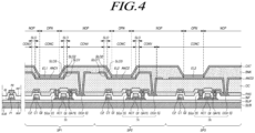
- FIG. 4 is a cross-sectional view illustrating the display device according to embodiments of the present disclosure.
- the substrate (SUB) is subdivided into areas corresponding to a first subpixel (SP1), a second subpixel (SP2) and a third subpixel (SP3).
- the first subpixel (SP1) emits visible light of a first color
- the second subpixel (SP2) emits visible light of a second color
- the third subpixel (SP3) emits visible light of a third color.
- the first subpixel (SP1), the second subpixel (SP2) and the third subpixel (SP3) can be also defined as a first subpixel type (SP1), a second subpixel type (SP2) and a third subpixel type (SP3), respectively. Accordingly, hereinafter, either the subpixel or the subpixel type will used interchangeably.
- the overcoat layer (OC) denotes a layer for planarizing at least one pattern layer disposed over the substrate for forming a pixel.
- the overcoat layer includes a convex area (CONV) and a concave area (CONC), which are connected to each other through an inclined area (SLO).
- the convex area (CONV) is thicker than the concave area (CONC).
- the thickness of the convex area (CONV) and the concave area (CONC) denotes a thickness of the overcoat layer.
- the thickness of the convex area (CONV) and the concave area (CONC) can be defined as a thickness of the overcoat layer measured between a passivation layer (PAS) disposed directly under the overcoat layer (OC) and an anode electrode (ANO) disposed directly on the overcoat layer (OC), in each area, and in particular, can be defined as the thickest thickness of the overcoat layer measured in each area except for a portion in which a contact hole, or the like is introduced.
- PAS passivation layer
- ANO anode electrode
- the thickness (T1) of the concave area (CONC) can be smaller than the thickness (T2) of the convex area (CONV). Accordingly, relative to the cross section of the display panel, the concave area (CONC) can be recognized as a flat area of the overcoat layer (OC), and the convex area (CONV) can be recognized as a protruding area.
- the inclined area (SLO) is formed between the convex area (CONV) and the concave area (CONC) due to a difference between the thicknesses of the convex area (CONV) and the concave area (CONC).
- the convex area (CONV) and the concave area (CONC) are connected to each other through the inclined area (SLO).
- the inclined area (SLO) includes a first inclined surface (SLO1) surrounding the concave area (CONC) in at least one of the first, second and third subpixel types (SP1, SP2 and SP3).
- the at least one of the first, second and third subpixel types can denote at least one type of subpixel, in which the type of the subpixel is classified according to a color of light emitted from the subpixel. For example, when a display panel includes a red subpixel, a green subpixel and a blue subpixel, the display panel can be expressed as including three types of subpixel.
- the first inclined surface (SLO1) denotes an inclined surface that is an inclined area surrounding the concave area (CONC) of inclined areas (SLO) formed between the convex area (CONV) and the concave area (CONC) of the overcoat layer (OC). Accordingly, in the display panel shown in FIG. 4 , the first subpixel (SP1) and the second subpixel (SP2) includes the inclined area, and thus includes the first inclined surface (SLO1). On the other hand, the third subpixel (SP3) does not include the inclined area surrounding the concave area (CONC), and thus does not include the first inclined surface (SLO1).
- the convex area (CONV) surrounds the concave area (CONC), in the cross section of the display panel, the concave area (CONC) is located between the convex areas (CONV).
- the overcoat layer (OC) including the convex area (CONV), the concave area (CONC) and the inclined area (SLO) can be formed through a photolithography process using a half-tone mask.
- the shape of the concave area (CONC) may preferably be, but not limited to, a polygonal shape, such as a circle or a square, a pentagon, and an octagon.
- the convex areas (CONV) can surround the concave area (CONC), and can form a side wall surrounding a side portion of the concave area (CONC) having the shape described above.
- the first anode electrode (ANO1), the second anode electrode (ANO2), a third anode electrode (ANO3), formed along a surface of the overcoat layer (OC), are located on the overcoat layer (OC) located over the substrate.
- the forming of the anode electrodes (ANO1, ANO2 and ANO3) along the surface of the overcoat layer (OC) can mean that the anode electrodes are formed on the overcoat layer with a thickness that is considered to be uniform when a thickness variation due to a tolerable process deviation is taken into account (e.g., the anodes can follow the contours of the surface of the overcoat layer).
- Each of the first anode electrode (ANO1), the second anode electrode (ANO2) and the third anode electrode (ANO3) can be spaced apart from one another by a certain distance, and can transfer independently a signal to a corresponding subpixel.
- the overcoat layer (OC) includes the first inclined surface (SLO1) surrounding the concave area (CONC) in at least one of the first, second and third subpixel types (SP1, SP2 and SP3). Accordingly, in a situation where the anode electrode is formed along a surface of the first inclined surface (SLO1) that is a part of the surface of the overcoat layer (OC), the anode electrode also includes an inclined surface. In the present disclosure, such an inclined surface of the anode electrode is referred to as a second inclined surface (SLO2).
- the second inclined surface (SLO2) is a shape surrounding the anode electrode portions formed on the concave area (CONC) of the overcoat layer (OC).
- the first, second and third anode electrodes can be electrically connected to one another through a contact hole.
- the anode electrode can be an electrode including a reflective electrode.
- the anode electrode can include a conductive metal oxide layer including indium tin oxide ITO and a reflective metal layer including silver.
- the anode electrode can include a first indium tin oxide ITO layer located on the overcoat layer, the reflective metal layer including silver located on the first indium tin oxide ITO layer, and a second indium tin oxide ITO layer located on the reflective metal layer.
- the anode electrodes can function as anode electrodes in the display panel.
- the bank layer (BNKl) includes an open area (BNKO) located in the center area of each of the first, second and third subpixels (SP1, SP2, SP3).
- the open area (BNKO) of the bank denotes an open area in which the bank layer does not cover the anode electrode, and can denote an area indicated by the OPN as shown in FIG. 4 .
- the open area (BNKO) of the bank denotes an open area formed in the bank layer, in which the anode electrode is exposed by the open area (BNKO) of the bank.
- the organic light emitting layer and the cathode electrode can be sequentially disposed on the exposed anode electrode. Accordingly, the open area (BNKO) of the bank is provided in the center area of each of the subpixels emitting light, and thus allows the subpixels to emit the light.
- the first organic light emitting layer (EL1) is located on a part of the first anode electrode (ANO1) located in the open area (BNKO) of the bank.
- the second organic light emitting layer (EL2) is located on a part of the second anode electrode (ANO2) located in the open area (BNKO) of the bank.
- the third organic light emitting layer (EL3) is located on a part of the third anode electrode (ANO3) located in the open area (BNKO) of the bank.
- the first, second and third organic light emitting layers are layers discharging light when an exciton having high energy formed from the recombination of a hole and an electron injected through an anode and a cathode falls into low energy
- the first, second and third organic light emitting layers are located on the exposed anode electrodes (ANO1, ANO2, ANO3) not covered by the open area (BNKO) of the bank.
- the anode electrodes (ANO1, ANO2, and ANO3) can be an anode.
- the cathode electrode (CAT) can be located on the organic light emitting layer (EL1, EL2, EL3) and the bank layer (BNK).
- the display panel can be a top emission type in which light emitted from the organic light emitting layer (EL1, EL2, EL3) is emitted through the cathode electrode (CAT).
- the cathode electrode (CAT) can be a transparent electrode with excellent transmittance to light in the visible light region
- the bank layer (BNK) can perform a function as a layer for distinguishing between an opening area (OPN) and a non-opening area (NOP) of the display panel.
- the display panel in the present disclosure can include two different types of areas, which are the opening area (OPN) and the non-opening area (NOP) subdivided by the configuration of the bank layer (BNK).
- the opening area (OPN) can correspond to the open area (BNKO) of the bank
- the non-opening area (NOP) can correspond to the bank layer (BNK) except for the open area (BNKO).
- the opening area (OPN) and the non-opening area (NOP) can be located in the active area (A/A) of the display panel.
- the correspondence of an area to another area may mean a relationship in which the one area and the another area are considered to be the same, taking into account tolerance that may occur in the manufacturing process of a product.
- the anode electrode (ANO1, ANO2, ANO3), the bank layer (BNK), the organic light emitting layer (EL1, EL2, EL3) and the cathode electrode (CAT) are located over the overcoat layer (OC)
- light can be emitted from the opening area (OPN) in which the anode electrode (ANO1, ANO2, ANO3), the organic light emitting layer (EL1, EL2, EL3) and the cathode electrode (CAT) in the open area (BNKO) of the bank layer are sequentially disposed.
- the display panel can include a buffer layer (BUF), a interlayer insulating film (INF), a passivation layer (PAS), a transistor (TR), a storage capacitor (C1, C2), an auxiliary electrode (AE, or may be referred to as an auxiliary line) and a pad area.
- BAF buffer layer
- INF interlayer insulating film
- PAS passivation layer
- TR transistor
- C1, C2 storage capacitor
- AE auxiliary electrode
- AE auxiliary electrode
- the buffer layer (BUF) can be disposed on the substrate (SUB), and the transistor (TR) and the storage capacitor (C1, C2), and the like can be disposed over the buffer layer (BUF).
- the interlayer insulating film (INF) can be located on a gate electrode (GATE) of the transistor (TR), an active layer (ACT), a first storage capacitor (C1) of the storage capacitor, and a first pad electrode (P1) of the pad area.
- GATE gate electrode
- ACT active layer
- C1 storage capacitor
- P1 first pad electrode
- the passivation layer (PAS) can be disposed to protect electronic elements, such as the auxiliary electrode (AE), the storage capacitor (C1, C2), the transistor (TR), and the like.
- the activation layer (ACT) can be disposed on the buffer layer (BUF).
- the gate insulating film (GI) is disposed on the activation layer (ACT), and the gate electrode (GATE) is disposed on the gate insulating film (GI). Therefore, the gate insulating film (GI) can be located between the activation layer (ACT) and the gate electrode (GATE).
- Each of the source electrode (S) and the drain electrode (D) can contact respective portions of the activation layer ACT, and be disposed spaced apart from each other.
- the drain electrode (D) can be connected to the anode electrode (ANO) through a contact hole.
- the transistor (TR) can function as a driving transistor (DRT) included in the panel, and drive the OLED included in the panel.
- DDT driving transistor
- the storage capacitor (C1, C2) can be disposed in the active area (A/A).
- the storage capacitor (C1, C2) can include a first storage capacitor electrode (C1) disposed in an identical layer to the gate electrode (GATE) and a second storage capacitor electrode (C2) disposed in an identical layer to the source electrode (S) and the drain electrode (D), but the structure of the storage capacitors (C1, C2) of the present disclosure is not limited thereto.
- the display panel according to embodiments of the present disclosure can include a pad area disposed in the non-active area.
- a plurality of pad electrodes (P1 and P2) can be disposed in the pad area.
- a first pad electrode (P1) can be disposed on the plurality of insulating films (BUF, GI) disposed in the pad area.
- the interlayer insulating film (INF) can be disposed on the first pad electrode (P1), a part of the top surface of which is not covered by the first pad electrode (P1).
- a second pad electrode (P2) that contacts the first pad electrode (P1) can be disposed over the first pad electrode (P1) and the interlayer insulating film (INF).
- various circuit films, or the like can be electrically connected to the second pad electrode (P2).
- FIG. 5 is a view illustrating how light emitted from any subpixel of the display panel can travel according to embodiments of the present disclosure.
- the subpixel shown in FIG 5 is a subpixel including the first inclined surface (SLO1), the second inclined surface (SLO2) and the third inclined surface (SLO3)
- the organic light emitting layer (EL) can be one of the first organic light emitting layer (EL1), second organic light emitting layer (EL2) and the third organic light emitting layer (EL3), and as described above, is an organic light emitting layer included in the subpixel including the first inclined surface (SLO1), the second inclined surface (SLO2) and the third inclined surface (SLO3).
- Some of light emitted from the organic light emitting layer (EL) may be totally reflected and travel toward third inclined surface (SLO3)of the bank layer (BNK), while traveling from a layer with a high refractive index to a layer with a low refractive index.
- SLO3 third inclined surface
- BNK bank layer
- the bank layer (BNK) is formed of a material with a certain range of transmittance to light in a visible light wavelength range. Accordingly, some light emitted toward the third inclined surface (SLO3)of the bank layer (BNK) can travel through the third inclined surface (SLO3)of the bank layer (BNK), and then reach the second inclined surface (SLO2) of the anode electrode (ANO).
- the anode electrode (ANO) is also one of the first anode electrode (ANO1) to the third anode electrode (ANO3). It should be understood that the anode electrode (ANO) is an anode electrode included in a subpixel including the first, second and third inclined surfaces.
- the structure can utilize the three different inclined surfaces from existing layers to provide three more chances to reflect light out of the device, thus improving light extraction without increasing the thickness of the device and without requiring separate reflective structures (e.g., edges of the overcoat layer, anode electrode and bank layer can be leveraged to provide additional functions, such as light extraction and reflection, and color shifting).
- the second inclined surface (SLO2) of the anode electrode (ANO) is reflected from the second inclined surface (SLO2), and then may travel toward the third inclined surface (SLO3)of the bank layer (BNK) and travel out of the display panel. Accordingly, as described above, in the display panel according to embodiments of the present disclosure, the second inclined surface (SLO2) of the anode electrode formed on the first inclined surface (SLO1) enables light emitted from the organic light emitting layer (EL) to travel toward an upper portion of the display panel, resulting in the luminous efficiency of the display panel being improved.
- FIG. 6 is an enlarged cross-sectional view illustrating a part of the subpixel shown in FIG. 5 according to embodiments of the present disclosure.
- an angle ( ⁇ ) between the concave area (CONC) and the first inclined surface (SLO1) is represented as ⁇ (hereinafter, referred to as " ⁇ ")
- ⁇ a distance between the second inclined surface (SLO2) and the third inclined surface (SLO3)
- d a distance between the second inclined surface (SLO2) and the third inclined surface (SLO3)
- d a distance between the second inclined surface (SLO2) and the third inclined surface
- d a height of the first inclined surface (SLO1) is represented as h (hereinafter, referred to as "h"). It may be understood that h is the distance from the lowermost point of the first inclined surface to the upper most point of the first inclined surface measured in a direction which is normal to the substrate.
- h is the distance equal to the length of the first inclined surface (measured as the shortest distance from the locus of its lowermost points to the locus of its uppermost points) multiplied by the sine of ⁇ .
- the display panel according to embodiments of the present disclosure can have specific values of ⁇ and d, or specific values of ⁇ , d and h.
- the angle ( ⁇ ) between the concave area (CONC) and the first inclined surface (SLO1) can be greater than or equal to 27°, or 45°.
- the second inclined surface (SLO2) can more effectively reflect light emitted from the organic light emitting layer (EL) formed on the anode electrode (ANO) not covered by the open area (BNKO) of the bank.
- the upper limit may be preferably less than or equal to 80°, 70°, or 65°.
- the angle ⁇ can be in a range of approximately 27° to 80°.
- the d that is the distance between the second inclined surface (SLO2) and the third inclined surface (SLO3) is defined as a distance from the second inclined surface (SLO2) to the third inclined surface (SLO3), measured in a parallel direction to the first area (A1) of the overcoat layer.
- the d can be less than or equal to 3.2 ⁇ m, 2.6 ⁇ m or 2.0 ⁇ m.
- the lower limit of the d may be preferably greater than or equal to 0.1 ⁇ m, 0.3 ⁇ m, or 0. 5 ⁇ m.
- the distance d can be in a range of approximately 0.1 ⁇ m to 3.2 ⁇ m.
- the h that is the height of the first inclined surface (SLO1) denote a difference between a thickness (T1') of the concave area (CONC) and a thickness (T2') of the convex area (CONV), which are connected by the first inclined surface (SLO1).
- the thickness (T1') of the concave area (CONC) can be a thickness of the concave area (CONC) measured at the beginning of the first inclined surface (SLO1).
- the thickness (T2') of the convex area (CONV) can be a thickness of the convex area (CONV) measured at the end of the second inclined surface (SLO2).
- the h can be preferably greater than or equal to 0.7 ⁇ m, 1.2 ⁇ m, 1.4 ⁇ m, or 2 ⁇ m.
- the upper limit may be preferably less than or equal to 10 ⁇ m, or 5 ⁇ m.
- the height h can be in a range of approximately 0.7 ⁇ m to 10 ⁇ m.
- the display panel according to the present disclosure can provide increased luminous efficiency and can include the first light emitting area and the second light emitting area when the organic light emitting layer emits light.
- FIGS. 7A and 7B show views illustrating the display panel including an opening area, a non-opening area, a first light emitting area, and a second light emitting area according to embodiments of the present disclosure.
- FIG. 7A shows a photomicrograph of the display panel including an opening area (OPN) and a non-opening area (NOP) having a specific shape.
- FIG. 7B shows a photomicrograph taken when the organic light emitting layer (EL1, EL2, EL3) of the display panel emits light. All subpixels shown in FIG. 7A include the first inclined surface (SLO1) to the third inclined surface (SLO3).
- the display panel according to the present disclosure can include a first light emitting area (LEA1) and a second light emitting area (LEA2), in which visible light is emitted when the organic light emitting layer emits light, and a first non-light emitting area (NEA1) and a second non-light emitting area (NEA2).
- the second non-light emitting area (NEA2) is included in a subpixel including the first inclined surface (SLO1), the second inclined surface (SLO2) and the third inclined surface (SLO3).
- the first light emitting area (LEA1) can have a shape corresponding to a shape of the opening area (OPN).
- the correspondence of a shape of an element to a shape of another element can mean that i ) the shape of the element is an identical shape to the another element, ii ) two elements have an identical shape, but have different sizes from each other, or iii) the shape of the element can be formed by transferring the shape of the another element.
- the shape of the first light emitting area (LEA1) can mean that the shape of the opening area (OPN) is substantially transferred by light emitted from the organic light emitting layer (EL1, EL2, EL3) located in the opening area (OPN).
- the shape of the opening area (OPN) can preferably be, but not limited to, a polygonal shape, such as a circle or a square, a pentagon, and an octagon. Referring to FIG. 7A , the opening area (OPN) has a shape corresponding to the octagon.
- the first light emitting area (LEA1) can have a shape corresponding to the opening area (OPN). Referring to FIG. 7B , the first light emitting area (LEA1) has a shape corresponding to the shape of opening area (OPN) as shown in FIG. 7A .
- the second light emitting area (LEA2) does not overlap the first light emitting area (LEA1).
- the second light emitting area (LEA2) can have a shape corresponding to a shape of an edge of the first light emitting area (LEA1).
- the second light emitting area (LEA2) has an identical shape to the edge of the first light emitting area (LEA1), but has different size from the first light emitting area (LEA1). Therefore, it is possible to express that the second light emitting area (LEA2) has a shape corresponding to the edge shape of the first light emitting area (LEA1).
- the second light emitting area (LEA2) can be a closed curve having an identical shape to the edge of the first light emitting area (LEA1).
- the second light emitting area (LEA2) can have a shape in which a part of the closed curve is disconnected. It is possible to determine whether the second light emitting area (LEA2) is disconnected, depending on a wavelength of visible light emitted from an organic light emitting layer included in a subpixel.
- At least one subpixel can be distinguished by the first light emitting area (LEA1).
- LSA1 first light emitting area
- each of a plurality of second light emitting areas (LEA2) can be spaced apart from one another by the first non-light emitting area (NEA1). That is, the first non-light emitting area (NEA1) can be an area between the second light emitting areas (LEA2) in the non-opening area (NOP).
- the first non-light emitting area (NEA1) can be substantially an area in which light emitting is not performed. That is, the first non-light emitting area (NEA1) can correspond to a part of the non-opening area (NOP), in which the second light emitting area (LEA2) is not formed,
- a light emitting area formed in one subpixel can be divided into the first light emitting area (LEA1) and the second light emitting area (LEA2) by the second non-light emitting area (NEA2).
- the second non-light emitting area (NEA2) may be an area in which light emitting is not substantially performed.
- a shape of the second non-light emitting area (NEA2) may be determined depending on the shapes of the first light emitting area (LEA1) and the second light emitting area (LEA2). For example, in a situation where the first light emitting area (LEA1) has an octagon shape, and the second light emitting area (LEA2) has a closed curve with the octagon shape, the second non-light emitting area (NEA2) can have the octagon shape by the first light emitting area (LEA1) and the second light emitting area (LEA2).
- the second non-light emitting area (NEA2) is described using the term of non-light emitting, it is possible for some light to be detected in the photograph because the second non-light emitting area (NEA2) is located between the light emitting areas (LEA1 and LEA2). In particular, it is possible for light with colors similar to a wavelength range of visible light emitted in the subpixel to be detected. Accordingly, the second non-light emitting area (NEA2) can be an area in which light emitting is not performed at all, or it should be understood that the second non-light emitting area (NEA2) can be an area in which light less than two light emitting areas is observed.
- the second light emitting area (LEA2) can be implemented by adjusting a range of the ⁇ , the d, or the h. Accordingly, the display panel according to embodiments of the present disclosure may have increased luminous efficiency and include the first light emitting area (LEA1) and the second light emitting area (LEA2), by adjusting a range of the ⁇ , the d, or the h.
- the second light emitting area (LEA2) can reflect light out of the device, which otherwise may not have been able to escape.
- the second light emitting area (LEA2) is formed by light traveling through paths described with reference to FIG. 5 .
- the subpixel shown in FIG. 5 includes, as well as the first light emitting area (LEA1), the second light emitting area (LEA2) formed by light reflected from the second inclined surface (SLO2). Therefore, it is possible to provide the display panel with increased luminous efficiency.
- the overcoat layer configured with the first inclined surface (SLO1) surrounding the concave area (CONC) is included in at least one of the first subpixel type to the third subpixel type, and thus it is possible to provide the display panel with enhanced luminous efficiency.
- the second light emitting area (LEA2) can surround the first light emitting area (LEA1). In other words, the second light emitting area (LEA2) can be located all around the first light emitting area (LEA1). It is believed that this is because the second light emitting area (LEA2) is formed by light reflected from the second inclined surface (SLO2) of the anode electrode (ANO) formed on the first inclined surface(SLO1) surrounding the concave area (CONC).
- the second light emitting area (LEA2) can be located in the non-opening area (NOP).
- NOP non-opening area
- light forming the first light emitting area (LEA1) and the second light emitting area (LEA2) travels through different paths and different layers, and therefore corresponding color coordinates may be different. That is, light forming the second light emitting area (LEA2) travels through the bank layer (BNK) in the non-opening area (NOP), while the light forming the first light emitting area (LEA1) does not travel through the bank layer.
- the bank layer (BNK) may absorb a portion of the light of a part of the wavelength of light forming the second light emitting area (LEA2), and therefore, the light forming the second light emitting area (LEA2) may have different color coordinates from the light forming the first light emitting area (LEA1).
- the difference of the color coordinates can mean that there is a difference that can be regarded as different, taking into account a typical error caused at the time of measuring the color coordinates.
- the second non-light emitting area (NEA2) is described using the term of non-light emitting, it is possible for some light to be detected in the photograph because the second non-light emitting area (NEA2) is located between the light emitting areas (LEA1 and LEA2). In particular, it is possible for light with colors similar to a wavelength range of visible light emitted in the subpixel to be detected. Accordingly, the second non-light emitting area (NEA2) can be an area in which light emitting is not performed at all, or it should be understood that the second non-light emitting area (NEA2) can be an area in which light less than two light emitting areas is observed.
- a plurality of the first light emitting areas and the second light emitting areas can be formed according to the number of subpixel areas included in the display panel, for example, the first subpixel, the second subpixel, the third subpixel, etc.
- the second light emitting area adjacent to the first light emitting area is a light emitting area included in an identical subpixel area, and denotes the second light emitting area adjacent to the first light emitting area of a plurality of the second light emitting areas. This is because a first light emitting area and a second light emitting area adjacent to the first light emitting area are located in one subpixel area, and a light emitting area is formed by light emitted from an identical organic light emitting layer.
- FIG. 8 is a view illustrating that light emitted from a subpixel of the display panel travels according to embodiments of the present disclosure. Unlike the subpixel shown in FIGS. 5 and 6 , the subpixel shown in FIG. 8 does not include the first inclined surface (SLO1) and the second inclined surface (SLO2). Accordingly, unlike the subpixels shown in FIGS. 5 and 6 , the subpixel includes only the first light emitting area (LEA1) without the second light emitting area (LEA2) formed.
- the subpixel having the structure shown in FIG. 5 includes the first light emitting area (LEA1) and the second light emitting area (LEA2), and light emitted from the second light emitting area (LEA2) has different color coordinates from light emitted from the first light emitting area (LEA1).
- a difference in the color coordinates results from a difference between a traveling path of light emitted from the first light emitting area (LEA1) and a traveling path of light emitted from the second light emitting area (LEA2). That is, a difference in traveling paths of the second light emitting area (LEA2) and the first light emitting area (LEA1) results in a variation in the color coordinates (e.g., a color shift).
- the variation of the color coordinates is affected by a wavelength range of light emitted from an organic light emitting layer. Accordingly, to prevent deterioration of the display panel due to the variation of the color coordinate, in the display including a first subpixel to a third subpixel (or, a first subpixel type to a third subpixel type) emitting a first color to a third color, i ) at least one type of subpixel can include the first inclined surface (SLO1), ii ) at least one of a first subpixel type and a second subpixel type can include the first inclined surface (SLO1), and iii) at least one of a first subpixel type and a second subpixel type can include the first inclined surface (SLO1) and a third subpixel type can be a type without the first inclined surface (SLO1).
- a subpixel including the first inclined surface (SLO1) can have a structure shown in FIG. 5
- a subpixel not including the first inclined surface (SLO1) can have a structure shown in FIG. 8 .
- the mixed subpixel types can help hide or avoid any detectable color shifts or undesirable color shifts.
- the subpixel having structure shown in FIG. 8 can be a subpixel emitting light in a wavelength range in which a degree of color variation resulted from the forming of the second light emitting area is large.
- visible light of a first color emitted from the first subpixel can be red visible light
- visible light of a second color emitted from the second subpixel can be green visible light
- visible light of a third color emitted from the third subpixel can be blue visible light.
- the visible light of the red color can denote visible light typically recognized as red when viewed through the naked eye or a photographing device, for example, visible light having a wavelength range of 595 nm to 740 nm.
- the visible light of the green color can denote visible light typically recognized as green when viewed through the naked eye or a photographing device, for example, visible light having a wavelength range of 495 nm to 595 nm.
- the visible light of the blue color can denote visible light typically recognized as blue when viewed through the naked eye or a photographing device, for example, visible light having a wavelength range of 450 nm to 495 nm.
- the first inclined surface can be absent from a subpixel emitting a color resulting in a large color variation, but can be included in a subpixel emitting a color resulting in a small color variation, resulted from the forming of the second light emitting area.
- the display panel with enhanced luminous efficiency, low quality deterioration according to angles of view, and an excellent color gamut.
- the display panel according to embodiments of the present disclosure may be configured to adjust the ⁇ , the d, and the h described above according to a color emitted from a subpixel.
- the overcoat layer includes the first inclined surface in at least two of the first subpixel type to the third subpixel type.
- An angle of the first inclined surface included in each of the first, second and third subpixel types can be different from one another.
- a distance between the second inclined surface and the third inclined surface in each of the first, second and third subpixel types is different from one another.
- a height of the first inclined surface included in each of the first, second and third subpixel types can be different from one another.
- Each type of subpixel can refer to a subpixel type that emits a different color from one another when a subpixel that emits light of a color is expressed as one type of subpixel.
- the display panel since the first subpixel (SP1) and the second subpixel (SP2) include the first inclined surface (SLO1), therefore, the display panel includes at least two of the first, second and third subpixel types.
- an angle ( ⁇ ) of a first inclined surface included in the first subpixel (SP1) can be adjusted differently from an angle ( ⁇ ) of a first inclined surface included in the second subpixel (SP2), taking into account characteristics of light of the different color.
- a distance (d) between the second inclined surface and the third inclined surface can be also adjusted differently for enabling a corresponding value measured in the first subpixel (SP1) to be different from a corresponding value measured in the second subpixel (SP2).
- a height (h) of the first inclined surface can be adjusted differently for enabling a height of a first inclined surface included in the first subpixel (SP1) to be different from a height of a first inclined surface included in the second subpixel (SP2).
- the ⁇ , the d and the h are adjusted differently depending on characteristics of the color of light emitted from each subpixel, it is possible to maximize light extraction efficiency (e.g., different colors may perform better with different settings for the ⁇ , the d and the h, based on the corresponding wavelengths).
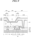
- FIG. 9 is a cross-sectional view illustrating the display device according to embodiments of the present disclosure.
- the organic light emitting layer (EL) can be disposed on parts of the anode electrode (ANO) that are not covered by the open area (BNKO) of the bank layer and the bank layer (BNK), for example, extending from a portion on the anode electrode (ANO) that is not covered by the open area (BNKO) of the bank layer to a portion on the bank layer (BNK).
- the cathode electrode (CAT) can be located on the organic light emitting layer (EL).
- FIG. 9 shows that the organic light emitting layer (EL) covers the whole top surface of the bank layer (BNK), but embodiments of the present disclosure are not limited thereto.
- the organic light emitting layer (EL) can be disposed to cover the open area (BNKO) of the bank layer and a part of the top surface of the bank layer (BNK).
- the organic light emitting layer (EL) is disposed across both the opening area (OPN) (in which the bank layer (BNK) is not disposed) and parts of the non-opening area (NOP) (in which the bank layer (BNK) is disposed), it is possible to maximize an area of the organic light emitting layer (EL) in which light emitting is performed.
- the organic light emitting layer (EL) is disposed in only the opening area (OPN) (e.g., not on parts of the bank layer)
- the organic light emitting layer (EL) may not be formed in an edge portion of the opening area (OPN) or may be incompletely formed.
- the organic light emitting layer (EL) is disposed on parts of the bank layer (BNK) as well, it is possible to overcome some problems with limitations in process.
- FIG. 10 is an enlarged cross-sectional view illustrating a part of the display device shown in FIG. 9 according to embodiments of the present disclosure.
- a thickness (t1) of the organic light emitting layer (EL) disposed on the anode electrode (ANO) is larger than a thickness (t2) of the organic light emitting layer (EL) disposed on the third inclined surface (SLO3)of the bank layer (BNK).
- the difference in the thicknesses of the organic light emitting layer can be caused by the third inclined surface (SLO3)of the bank layer (BNK).
- the organic light emitting layer (EL) can be formed by a thermal evaporation process, which is a physical vapor deposition technique.
- the thermal evaporation process is used on the inclined surface, such as the third inclined surface (SLO3), the thickness of the deposited layer may reduce due to characteristics of the thermal deposition process,
- the density of carriers may increase at an electrode adjacent to the organic light emitting layer with the thin thickness and result in the organic light emitting layer being deteriorated.
- the bank layer (BNK) is located between the anode electrode (ANO) and the organic light emitting layer (EL), in a portion in which the organic light emitting layer (EL) has the thinned thickness (t2), as shown in FIG. 10 .
- the bank layer can help separate the thin portion of the organic light emitting layer (EL) to be just far enough away (e.g., distance "d") from the anode so that the density of carriers at the thin part of the organic light emitting layer (EL) does not unduly increase and prevents the organic light emitting layer from being prematurely deteriorated.
- Table 1 shows the observation on light emitting of the second light emitting area according to the variations of the ⁇ , the d and the h in a subpixel including the first inclined surface.
- the subpixels used for observing whether the second light emitting area is formed in the Table 1 have the structure shown in FIG. 9 .
- [Table 1] ⁇ (°) h( ⁇ m) d( ⁇ m) Whether the second light emitting area is formed Comparative example 1 8 0.6 2 X Comparative example 2 25 1.7 2 X Comparative example 3 25.8 1.7 2 X Embodiment 1. 45 1.4 2 O Embodiment 2. 60 2 2 O Embodiment 3. 60 2.04 2 O
- the second light emitting area is formed when i ) the ⁇ is greater than or equal to 27°, 35°, or 45°, ii ) the h is greater than or equal to 0.7 ⁇ m, 1.0 ⁇ m, or 1.4 ⁇ m, and iii) the d is less than or equal to 3.2 ⁇ m. Accordingly, the second light emitting area is formed in subpixels including the first inclined surface, and therefore, it is expected to exhibit excellent luminous efficiency.
- Table 2 shows luminous efficiency, degradation of display quality of images according to angles of view, and a color gamut.
- the Embodiments 4 to 6 (embodiments 4, 5 not forming part of the claimed invention) and the Comparative example 4 are display panels including three types of subpixel, such as, a red subpixel, a green subpixel, and a blue subpixel.
- all three types of subpixel do not include the first inclined surface, and each subpixel has a structure similar to that shown in FIG. 8 .
- the Embodiment 4, not forming part of the claimed invention only the red subpixel includes the first inclined surface.
- the Embodiment 5, not forming part of the claimed invention only the green subpixel includes the first inclined surface.
- the red and green subpixels include the first inclined surface.
- the Embodiment 6 has the structure of FIG. 4
- the Embodiments 4 and 5 are the same as the Embodiment 6, except that only one type of subpixel has the first inclined surface.
- FIGS. 11 and 12 relate to the display panel of the Comparative example 4.
- FIGS. 11(b) and 12(b) relate to the Embodiment 4.
- FIGS. 11(c) and 12(c) relate to the Embodiment 5.
- FIGS. 11(d) and 12(d) relate to the Embodiment 6.
- a display panel having configurations of the Embodiments 4 to 6, in which at least one subpixel of the red subpixel and the green subpixel includes the first inclined surface, and the blue subpixel does not include the first inclined surface has enhanced luminous efficiency and low degradation of display quality of images according to angles of view, compared with a display panel having configurations of the Comparative example 4 in which all the subpixels do not include the first inclined surface.
Landscapes
- Physics & Mathematics (AREA)
- Engineering & Computer Science (AREA)
- Microelectronics & Electronic Packaging (AREA)
- Optics & Photonics (AREA)
- Nonlinear Science (AREA)
- Geometry (AREA)
- Mathematical Physics (AREA)
- Chemical & Material Sciences (AREA)
- Crystallography & Structural Chemistry (AREA)
- General Physics & Mathematics (AREA)
- Electroluminescent Light Sources (AREA)
- Devices For Indicating Variable Information By Combining Individual Elements (AREA)
Claims (14)
- Anzeigetafel, umfassend:ein Substrat (SUB), das ein erstes, ein zweites und ein drittes Subpixel (SP1, SP2, SP3) beinhaltet, die jeweils konfiguriert sind zum Abstrahlen von Licht in voneinander verschiedenen Farben;eine Überzugsschicht (OC), die über dem Substrat angebracht ist und einen konkaven Bereich (CONC) und einen konvexen Bereich (CONV), die über eine erste geneigte Oberfläche (SLO1) miteinander verbunden sind, wobei die erste geneigte Oberfläche den konkaven Bereich bei mindestens zwei der ersten, zweiten und dritten Subpixel umgibt, und wobei der konvexe Bereich dicker als der konkave Bereich ist;eine erste, eine zweite und eine dritte Anodenelektrode(ANO1, ANO2, ANO3), die dem ersten, dem zweiten bzw. dem dritten Subpixel entsprechen, und entlang einer Oberfläche der Überzugsschicht gebildet sind, wobei mindestens zwei der ersten, der zweiten und der dritten Anodenelektrode eine zweite geneigte Oberfläche (SL02) beinhalten, die sich mit der ersten geneigten Oberfläche der Überzugsschicht überschneidet, und wobei die zweite geneigte Oberfläche die Abschnitte der Anodenelektroden umgibt, die in dem konkaven Bereich der Überzugsschicht gebildet sind;eine erste, eine zweite und eine dritte organische lichtemittierende Schicht (EL1, EL2, EL3) die an der ersten, der zweiten bzw. der dritten Anodenelektrode angebracht sind; undeine Bankschicht (BNK), die an der Überzugsschicht angebracht ist und einen offenen Bereich beinhaltet, der den konkaven Bereich der Überzugsschicht bei jedem des ersten, des zweiten und des dritten Subpixels überschneidet, wobei die Bankschicht eine dritte geneigte Oberfläche (SL03) beinhaltet, die sich sowohl mit der ersten geneigten Oberfläche der Überzugsschicht als auch mit der zweiten geneigten Oberfläche der mindestens zwei der ersten, der zweiten und der dritten Anodenelektrode überschneidet,wobei mindestens eine der ersten, der zweiten und der dritten geneigten Oberfläche konfiguriert ist zum Reflektieren von Licht, das von einer entsprechenden der ersten, der zweiten und der dritten organischen lichtemittierenden Fläche abgestrahlt wird,wobei ein Abstand d zwischen der zweiten geneigten Oberfläche und der dritten geneigten Oberfläche bei jedem des ersten, des zweiten und des dritten Subpixeltyps jeweils unterschiedlich von einem anderen ist, wobei der Abstand d parallel zu dem Substrat gemessen wird.
- Anzeigetafel nach Anspruch 1, wobei ein spitzer Winkel (Θ) zwischen der ersten geneigten Oberfläche der Überzugsschicht und einer imaginären Linie parallel zu einer Oberseite des konkaven Bereichs in einem Bereich von ungefähr 27° bis 80° liegt, wobei der Abstand d zwischen der zweiten geneigten Oberfläche der mindestens zwei der ersten, der zweiten und der dritten Anodenelektrode und der dritten geneigten Oberfläche der Bankschicht in einem Bereich von ungefähr 0,1 µm bis 3,2 µm liegt, und
wobei die Höhe der ersten geneigten Oberfläche der Überzugsschicht in einem Bereich von ungefähr 0,7 µm bis 10 µm liegt. - Anzeigetafel nach Anspruch 1 oder 2, wobei eine Grenzfläche zwischen der Bankschicht und einer der ersten, der zweiten und der dritten Anodenelektrode konfiguriert ist zum Reflektieren von Licht, das von einer entsprechenden der ersten, der zweiten und der dritten organischen lichtemittierenden Fläche abgestrahlt wird, und/oder
wobei eine Grenzfläche zwischen einer der ersten, der zweiten und der dritten Anodenelektrode und der Überzugsschicht konfiguriert ist zum Reflektieren von Licht, das von der entsprechenden der ersten, der zweiten und der dritten organischen lichtemittierenden Schicht abgestrahlt wird, um ein farbverschobenes Licht zu erzeugen und um das farbverschobene Licht zu reflektieren. - Anzeigetafel nach einem der vorhergehenden Ansprüche, wobei eine Grenzfläche zwischen der Bankschicht und einer der ersten, der zweiten und der dritten Anodenelektrode konfiguriert ist zum Verschieben einer Farbe von Licht, das von der entsprechenden der ersten, der zweiten und der dritten organischen lichtemittierenden Schicht abgestrahlt wird, um ein farbverschobenes Licht zu erzeugen, und/oder
wobei eine Grenzfläche zwischen einer der ersten, der zweiten und der dritten Anodenelektrode und der Überzugsschicht konfiguriert ist zum Verschieben einer Farbe von Licht, das von der entsprechenden der ersten, der zweiten und der dritten organischen lichtemittierenden Schicht abgestrahlt wird, um ein farbverschobenes Licht zu erzeugen. - Anzeigetafel nach einem der vorhergehenden Ansprüche, wobei ein Abschnitt der Bankschicht zwischen einem Abschnitt von mindestens einer der ersten, der zweiten und der dritten organischen lichtemittierenden Schicht und der ersten und der zweiten geneigten Oberfläche angebracht ist, und/oder
wobei sich mindestens ein Abschnitt der ersten, der zweiten und der dritten organischen lichtemittierenden Schicht mit der ersten, der zweiten und der dritten geneigten Oberfläche überschneidet. - Anzeigetafel nach einem der vorhergehenden Ansprüche,
wobei eine Höhe der ersten geneigten Oberfläche, die in jeder der mindestens zwei des ersten, des zweiten und des dritten Subpixels enthalten ist, jeweils unterschiedlich von einer anderen ist. - Anzeigetafel nach einem der vorhergehenden Ansprüche, wobei die Anzeigetafel einen Öffnungsbereich (OPN), der dem offenen Bereich der Bankschicht entspricht und einen Nicht-Öffnungsbereich (NOP) beinhaltet, der einem verbleibenden Bereich mit Ausnahme des offenen Bereichs der Bankschicht entspricht, und
wobei die Subpixel, welche die erste geneigte Oberfläche aufweisen, ferner beinhalten:einen ersten lichtemittierenden Bereich (LEA1), der konfiguriert ist zum Abstrahlen eines sichtbaren Lichts von einer entsprechenden lichtemittierenden Schicht und der eine Form aufweist, die einer Form des Öffnungsbereichs entspricht;einen zweiten lichtemittierenden Bereich (LEA2), der konfiguriert ist zum Reflektieren eines Teils des sichtbaren Lichts, das von der entsprechenden lichtemittierenden Schicht abgestrahlt wird, wobei der zweite lichtemittierende Bereich den ersten lichtemittierenden Bereich umgibt, ohne sich mit dem ersten lichtemittierenden Bereich zu überschneiden, und eine Form aufweist, die einer Form eines Rands des ersten lichtemittierenden Bereichs entspricht;einen ersten nicht-lichtemittierenden Bereich (NEA1), der sich außerhalb des zweiten lichtemittierenden Bereichs befindet; undeinen zweiten nicht-lichtemittierenden Bereich (NEA2), der sich zwischen dem ersten lichtemittierenden Bereich und dem zweiten lichtemittierenden Bereich befindet, wobei sich der zweite lichtemittierende Bereich optional in dem Nicht-Öffnungsbereich befindet. - Anzeigetafel nach Anspruch 7, wobei der zweite lichtemittierende Bereich einer Grenzfläche zwischen der Bankschicht und einer der ersten, der zweiten und der dritten Anodenelektrode oder einer Grenzfläche zwischen einer der ersten, der zweiten und der dritten Anodenelektrode und der Überzugsschicht entspricht.
- Anzeigetafel nach Anspruch 7 oder 8, wobei die Farbkoordinaten des sichtbaren Lichts, das von dem ersten lichtemittierenden Bereich abgestrahlt wird, verschieden sind von den Farbkoordinaten des sichtbaren Lichts, das von dem zweiten lichtemittierenden Bereich abgestrahlt wird, der sich in der Nähe des ersten lichtemittierenden Bereichs befindet, und
wobei sowohl das sichtbare Licht, das von dem ersten lichtemittierenden Bereich abgestrahlt wird, als auch das sichtbare Licht, das von dem zweiten lichtemittierenden Bereich abgestrahlt wird, auf einem Licht beruhen, das von der entsprechenden lichtemittierende Schicht abgestrahlt wird. - Anzeigetafel nach einem der vorhergehenden Ansprüche, wobei ein Abschnitt von mindestens einer der ersten, der zweiten und der dritten organischen lichtemittierenden Schicht, der sich mit einer entsprechenden Anodenelektrode überschneidet, dicker ist als ein anderer Abschnitt der mindestens einen der ersten, der zweiten und der dritten organischen lichtemittierenden Schicht, der sich mit der dritten geneigten Oberfläche der Bankschicht überschneidet.
- Anzeigetafel nach einem der vorhergehenden Ansprüche, die ferner umfasst:
eine erste Kontaktöffnung in der Überzugsschicht, die dem ersten Subpixel entspricht;eine zweite Kontaktöffnung in der Überzugsschicht, die dem zweiten Subpixel entspricht; und eine dritte Kontaktöffnung in der Überzugsschicht, die dem dritten Subpixel entspricht,wobei die Überzugsschicht in Bereichen, die sich mit der ersten und der zweiten organischen lichtemittierenden Schicht überschneiden, eine erste Dicke aufweist, und in Bereichen außerhalb der ersten und der zweiten organischen lichtemittierenden Schicht in der Nähe des ersten bzw. der zweiten Kontaktöffnung, eine zweite Dicke aufweist,wobei die Bankschicht in einem Bereich, der sich mit der dritten Kontaktöffnung in der Überzugsschicht überschneidet, eine dritte Dicke aufweist, undwobei die dritte Dicke größer als die zweite Dicke ist, und wobei die zweite Dicke größer als die erste Dicke ist. - Anzeigetafel nach einem der vorhergehenden Ansprüche, wobei die erste, die zweite und die dritte geneigte Oberfläche in dem ersten und dem zweiten Subpixel parallel zueinander sind, und
wobei die Überzugsschicht und die dritte Anodenelektrode, in einem Bereich, der sich mit der dritten geneigten Oberfläche in dem dritten Subpixel überschneidet, flach sind. - Anzeigetafel nach einem der vorhergehenden Ansprüche, die ferner umfasst:einen ersten lichtemittierenden Bereich und einen zweiten lichtemittierenden Bereich in dem ersten Subpixel;einen ersten lichtemittierenden Bereich und einen zweiten lichtemittierenden Bereich in dem zweiten Subpixel; undeinen ersten lichtemittierenden Bereich in dem dritten Subpixel,wobei sich der erste lichtemittierende Bereich in dem ersten, dem zweiten und dem dritten Subpixel mit der ersten, der zweiten bzw. der dritten organischen lichtemittierenden Schicht überschneiden, undwobei sich der zweite lichtemittierende Bereich in dem ersten und dem zweiten Subpixel mit der ersten, der zweiten bzw. der dritten geneigten Oberfläche in dem ersten bzw. dem zweiten Subpixel überschneidet, wobei der zweite lichtemittierende Bereich in dem ersten Subpixel optional eine andere Farbe abstrahlt als der erste lichtemittierende Bereich in dem ersten Subpixel.
- Anzeigevorrichtung, umfassend:Anzeigetafel nach einem der vorhergehenden Ansprüche; undeine Ansteuerungsschaltung, die konfiguriert ist zum Ansteuern der Anzeigetafel, wobei die Ansteuerungsschaltung einen Datentreiber zum Ansteuern einer Vielzahl von Datenleitungen und einen Gate-Treiber zum Ansteuern einer Vielzahl von Gate-Leitungen beinhaltet.
Applications Claiming Priority (1)
| Application Number | Priority Date | Filing Date | Title |
|---|---|---|---|
| KR1020180163604A KR102075728B1 (ko) | 2018-12-17 | 2018-12-17 | 표시패널 |
Publications (3)
| Publication Number | Publication Date |
|---|---|
| EP3671881A2 EP3671881A2 (de) | 2020-06-24 |
| EP3671881A3 EP3671881A3 (de) | 2020-07-01 |
| EP3671881B1 true EP3671881B1 (de) | 2025-06-11 |
Family
ID=68944193
Family Applications (1)
| Application Number | Title | Priority Date | Filing Date |
|---|---|---|---|
| EP19216938.1A Active EP3671881B1 (de) | 2018-12-17 | 2019-12-17 | Anzeigetafel |
Country Status (6)
| Country | Link |
|---|---|
| US (2) | US11189815B2 (de) |
| EP (1) | EP3671881B1 (de) |
| JP (3) | JP6926179B2 (de) |
| KR (1) | KR102075728B1 (de) |
| CN (2) | CN116528627A (de) |
| TW (2) | TWI751053B (de) |
Families Citing this family (17)
| Publication number | Priority date | Publication date | Assignee | Title |
|---|---|---|---|---|
| KR102075741B1 (ko) | 2018-12-17 | 2020-02-10 | 엘지디스플레이 주식회사 | 표시패널 |
| CN109873023B (zh) * | 2019-03-29 | 2021-10-19 | 京东方科技集团股份有限公司 | 一种oled显示基板及其制备方法、显示装置 |
| US11038150B1 (en) * | 2020-01-30 | 2021-06-15 | Sharp Kabushiki Kaisha | QLED/OLED pixel having reflective cavity electrode configuration |
| US11980046B2 (en) * | 2020-05-27 | 2024-05-07 | Taiwan Semiconductor Manufacturing Company, Ltd. | Method for forming an isolation structure having multiple thicknesses to mitigate damage to a display device |
| EP4182981A4 (de) * | 2020-07-16 | 2024-05-22 | Applied Materials, Inc. | Reflektierende strukturen mit gradiertem gradienten für oled anzeigepixel |
| CN114843422A (zh) * | 2020-09-03 | 2022-08-02 | 京东方科技集团股份有限公司 | 显示面板及其制造方法、显示装置 |
| JP7014459B1 (ja) * | 2020-09-25 | 2022-02-01 | ソニーセミコンダクタソリューションズ株式会社 | 表示装置および電子機器 |
| KR20220096229A (ko) | 2020-12-30 | 2022-07-07 | 엘지디스플레이 주식회사 | 발광 표시 장치 |
| CN113380862B (zh) * | 2021-05-31 | 2023-12-22 | 合肥维信诺科技有限公司 | 显示面板及其制备方法 |
| CN115548231B (zh) * | 2021-06-29 | 2025-09-19 | 京东方科技集团股份有限公司 | 一种显示面板及显示装置 |
| KR20230064452A (ko) * | 2021-11-03 | 2023-05-10 | 엘지디스플레이 주식회사 | 표시 장치 |
| CN114122086B (zh) * | 2021-11-11 | 2023-12-01 | 深圳市华星光电半导体显示技术有限公司 | 显示面板及其制备方法与移动终端 |
| KR102902751B1 (ko) * | 2021-12-28 | 2025-12-19 | 엘지디스플레이 주식회사 | 투명 표시 장치 |
| KR20230101124A (ko) * | 2021-12-29 | 2023-07-06 | 엘지디스플레이 주식회사 | 디스플레이 장치 |
| KR20240110120A (ko) * | 2022-12-29 | 2024-07-15 | 엘지디스플레이 주식회사 | 표시장치 |
| KR20240176682A (ko) * | 2023-06-16 | 2024-12-24 | 엘지디스플레이 주식회사 | 표시 장치 및 표시 패널 |
| KR20250132935A (ko) * | 2024-02-29 | 2025-09-05 | 엘지디스플레이 주식회사 | 표시 장치 |
Family Cites Families (26)
| Publication number | Priority date | Publication date | Assignee | Title |
|---|---|---|---|---|
| JPH04291492A (ja) | 1991-03-20 | 1992-10-15 | Fuji Electric Co Ltd | 自動販売機の冷却装置 |
| JP2012113934A (ja) * | 2010-11-24 | 2012-06-14 | Canon Inc | 表示装置 |
| JP2012199231A (ja) * | 2011-03-04 | 2012-10-18 | Semiconductor Energy Lab Co Ltd | 表示装置 |
| KR101881133B1 (ko) * | 2011-06-29 | 2018-07-24 | 삼성디스플레이 주식회사 | 절연층의 경사 구조 형성 방법, 유기 발광 표시 장치 및 유기 발광 표시 장치의 제조 방법 |
| KR101900954B1 (ko) * | 2012-01-19 | 2018-09-21 | 삼성디스플레이 주식회사 | 유기 발광 표시 장치 및 유기 발광 표시 장치의 제조방법 |
| EP2852256A4 (de) | 2012-06-20 | 2016-04-27 | Pioneer Corp | Organische elektrolumineszenzvorrichtung |
| TW201442226A (zh) | 2013-03-21 | 2014-11-01 | 新力股份有限公司 | 顯示裝置及其製造方法、以及電子機器 |
| JP2015050011A (ja) * | 2013-08-30 | 2015-03-16 | 株式会社ジャパンディスプレイ | エレクトロルミネセンス装置およびその製造方法 |
| JP2015069844A (ja) * | 2013-09-30 | 2015-04-13 | ソニー株式会社 | 表示装置および電子機器 |
| JP6517597B2 (ja) * | 2015-06-10 | 2019-05-22 | 株式会社ジャパンディスプレイ | 表示装置 |
| KR102358542B1 (ko) * | 2015-07-31 | 2022-02-04 | 엘지디스플레이 주식회사 | 유기발광다이오드 패널 및 유기발광다이오드 표시장치와 그 제조방법 |
| KR102626853B1 (ko) * | 2015-10-30 | 2024-01-18 | 삼성디스플레이 주식회사 | 유기 발광 표시 장치 |
| JP2017091802A (ja) * | 2015-11-10 | 2017-05-25 | 株式会社Joled | 有機el表示パネル、および、有機el表示パネルの製造方法 |
| CN105609534A (zh) * | 2016-01-06 | 2016-05-25 | 京东方科技集团股份有限公司 | 一种oled显示基板及显示装置 |
| JP6561284B2 (ja) * | 2016-01-27 | 2019-08-21 | 株式会社Joled | 表示装置 |
| CN105870154B (zh) * | 2016-04-28 | 2019-04-05 | 京东方科技集团股份有限公司 | 一种阵列基板及其制备方法、oled显示装置 |
| KR102387859B1 (ko) * | 2016-09-30 | 2022-04-15 | 엘지디스플레이 주식회사 | 유기 발광 표시 장치 및 그 제조 방법 |
| KR102717809B1 (ko) | 2016-11-30 | 2024-10-15 | 엘지디스플레이 주식회사 | 발광 구조물을 포함하는 디스플레이 장치 |
| JP6943563B2 (ja) * | 2016-11-30 | 2021-10-06 | 株式会社ジャパンディスプレイ | 入力機能付き表示装置 |
| US10181574B2 (en) * | 2016-12-29 | 2019-01-15 | Lg Display Co., Ltd. | Organic light emitting device |
| KR102783429B1 (ko) * | 2017-01-25 | 2025-03-18 | 삼성디스플레이 주식회사 | 표시 장치 |
| KR102797659B1 (ko) * | 2017-02-10 | 2025-04-22 | 삼성디스플레이 주식회사 | 유기 발광 표시 장치 |
| CN106992203B (zh) * | 2017-04-24 | 2020-03-27 | 京东方科技集团股份有限公司 | 发光结构、显示面板及显示装置 |
| KR102603232B1 (ko) * | 2018-07-27 | 2023-11-15 | 엘지디스플레이 주식회사 | 표시장치 |
| KR102075741B1 (ko) * | 2018-12-17 | 2020-02-10 | 엘지디스플레이 주식회사 | 표시패널 |
| KR102087102B1 (ko) * | 2018-12-17 | 2020-04-20 | 엘지디스플레이 주식회사 | 유기발광 표시패널 및 이를 포함하는 유기발광 표시장치 |
-
2018
- 2018-12-17 KR KR1020180163604A patent/KR102075728B1/ko active Active
-
2019
- 2019-12-10 CN CN202310540223.6A patent/CN116528627A/zh active Pending
- 2019-12-10 CN CN201911257455.0A patent/CN111326670B/zh active Active
- 2019-12-11 JP JP2019223327A patent/JP6926179B2/ja active Active
- 2019-12-16 US US16/716,309 patent/US11189815B2/en active Active
- 2019-12-17 TW TW110109536A patent/TWI751053B/zh active
- 2019-12-17 EP EP19216938.1A patent/EP3671881B1/de active Active
- 2019-12-17 TW TW108146232A patent/TWI725671B/zh active
-
2021
- 2021-08-04 JP JP2021127964A patent/JP7242776B2/ja active Active
- 2021-10-25 US US17/509,959 patent/US12446404B2/en active Active
-
2023
- 2023-03-08 JP JP2023035493A patent/JP7612736B2/ja active Active
Also Published As
| Publication number | Publication date |
|---|---|
| JP2020098777A (ja) | 2020-06-25 |
| JP7242776B2 (ja) | 2023-03-20 |
| CN111326670B (zh) | 2023-05-30 |
| EP3671881A2 (de) | 2020-06-24 |
| CN116528627A (zh) | 2023-08-01 |
| US20200194713A1 (en) | 2020-06-18 |
| TW202125865A (zh) | 2021-07-01 |
| JP7612736B2 (ja) | 2025-01-14 |
| TWI751053B (zh) | 2021-12-21 |
| US11189815B2 (en) | 2021-11-30 |
| JP6926179B2 (ja) | 2021-08-25 |
| JP2023065673A (ja) | 2023-05-12 |
| JP2021180188A (ja) | 2021-11-18 |
| KR102075728B1 (ko) | 2020-02-10 |
| CN111326670A (zh) | 2020-06-23 |
| US20220045297A1 (en) | 2022-02-10 |
| TW202025533A (zh) | 2020-07-01 |
| TWI725671B (zh) | 2021-04-21 |
| US12446404B2 (en) | 2025-10-14 |
| EP3671881A3 (de) | 2020-07-01 |
Similar Documents
| Publication | Publication Date | Title |
|---|---|---|
| US12446404B2 (en) | Display panel with configuration for enhanced luminance efficiency | |
| US12342686B2 (en) | Display panel | |
| EP3671852B1 (de) | Organische lichtemittierende anzeigetafel und organische lichtemittierende anzeigevorrichtung damit | |
| US20210074955A1 (en) | Organic light emitting display panel and organic light emitting display device including the same | |
| US11758769B2 (en) | Organic light emitting display panel having improved light efficiency and organic light emitting display device including the same | |
| US20260033141A1 (en) | Display device | |
| CN121751902A (zh) | 显示装置 |
Legal Events
| Date | Code | Title | Description |
|---|---|---|---|
| PUAI | Public reference made under article 153(3) epc to a published international application that has entered the european phase |
Free format text: ORIGINAL CODE: 0009012 |
|
| STAA | Information on the status of an ep patent application or granted ep patent |
Free format text: STATUS: REQUEST FOR EXAMINATION WAS MADE |
|
| PUAL | Search report despatched |
Free format text: ORIGINAL CODE: 0009013 |
|
| 17P | Request for examination filed |
Effective date: 20191217 |
|
| AK | Designated contracting states |
Kind code of ref document: A2 Designated state(s): AL AT BE BG CH CY CZ DE DK EE ES FI FR GB GR HR HU IE IS IT LI LT LU LV MC MK MT NL NO PL PT RO RS SE SI SK SM TR |
|
| AX | Request for extension of the european patent |
Extension state: BA ME |
|
| AK | Designated contracting states |
Kind code of ref document: A3 Designated state(s): AL AT BE BG CH CY CZ DE DK EE ES FI FR GB GR HR HU IE IS IT LI LT LU LV MC MK MT NL NO PL PT RO RS SE SI SK SM TR |
|
| AX | Request for extension of the european patent |
Extension state: BA ME |
|
| RIC1 | Information provided on ipc code assigned before grant |
Ipc: H01L 51/52 20060101AFI20200526BHEP Ipc: H01L 27/32 20060101ALI20200526BHEP |
|
| RBV | Designated contracting states (corrected) |
Designated state(s): AL AT BE BG CH CY CZ DE DK EE ES FI FR GB GR HR HU IE IS IT LI LT LU LV MC MK MT NL NO PL PT RO RS SE SI SK SM TR |
|
| STAA | Information on the status of an ep patent application or granted ep patent |
Free format text: STATUS: EXAMINATION IS IN PROGRESS |
|
| 17Q | First examination report despatched |
Effective date: 20230202 |
|
| REG | Reference to a national code |
Ref country code: DE Ref legal event code: R079 Ipc: H10K0059122000 Ref country code: DE Ref legal event code: R079 Ref document number: 602019070997 Country of ref document: DE Free format text: PREVIOUS MAIN CLASS: H01L0051520000 Ipc: H10K0059122000 |
|
| GRAP | Despatch of communication of intention to grant a patent |
Free format text: ORIGINAL CODE: EPIDOSNIGR1 |
|
| STAA | Information on the status of an ep patent application or granted ep patent |
Free format text: STATUS: GRANT OF PATENT IS INTENDED |
|
| RIC1 | Information provided on ipc code assigned before grant |
Ipc: H10K 50/856 20230101ALI20241212BHEP Ipc: H10K 50/818 20230101ALI20241212BHEP Ipc: H10K 50/813 20230101ALI20241212BHEP Ipc: H10K 59/80 20230101ALI20241212BHEP Ipc: H10K 59/124 20230101ALI20241212BHEP Ipc: H10K 59/122 20230101AFI20241212BHEP |
|
| INTG | Intention to grant announced |
Effective date: 20250102 |
|
| RIN1 | Information on inventor provided before grant (corrected) |
Inventor name: YOO, NAMSEOK Inventor name: LEE, SUNMI Inventor name: LEE, SEONGJOO Inventor name: BEAK, JUNGSUN Inventor name: KIM, MI-NA |
|
| GRAS | Grant fee paid |
Free format text: ORIGINAL CODE: EPIDOSNIGR3 |
|
| GRAA | (expected) grant |
Free format text: ORIGINAL CODE: 0009210 |
|
| STAA | Information on the status of an ep patent application or granted ep patent |
Free format text: STATUS: THE PATENT HAS BEEN GRANTED |
|
| AK | Designated contracting states |
Kind code of ref document: B1 Designated state(s): AL AT BE BG CH CY CZ DE DK EE ES FI FR GB GR HR HU IE IS IT LI LT LU LV MC MK MT NL NO PL PT RO RS SE SI SK SM TR |
|
| REG | Reference to a national code |
Ref country code: GB Ref legal event code: FG4D |
|
| REG | Reference to a national code |
Ref country code: CH Ref legal event code: EP |
|
| REG | Reference to a national code |
Ref country code: IE Ref legal event code: FG4D |
|
| REG | Reference to a national code |
Ref country code: DE Ref legal event code: R096 Ref document number: 602019070997 Country of ref document: DE |
|
| REG | Reference to a national code |
Ref country code: NL Ref legal event code: FP |
|
| PG25 | Lapsed in a contracting state [announced via postgrant information from national office to epo] |
Ref country code: FI Free format text: LAPSE BECAUSE OF FAILURE TO SUBMIT A TRANSLATION OF THE DESCRIPTION OR TO PAY THE FEE WITHIN THE PRESCRIBED TIME-LIMIT Effective date: 20250611 Ref country code: ES Free format text: LAPSE BECAUSE OF FAILURE TO SUBMIT A TRANSLATION OF THE DESCRIPTION OR TO PAY THE FEE WITHIN THE PRESCRIBED TIME-LIMIT Effective date: 20250611 |
|
| REG | Reference to a national code |
Ref country code: LT Ref legal event code: MG9D |
|
| PG25 | Lapsed in a contracting state [announced via postgrant information from national office to epo] |
Ref country code: GR Free format text: LAPSE BECAUSE OF FAILURE TO SUBMIT A TRANSLATION OF THE DESCRIPTION OR TO PAY THE FEE WITHIN THE PRESCRIBED TIME-LIMIT Effective date: 20250912 Ref country code: NO Free format text: LAPSE BECAUSE OF FAILURE TO SUBMIT A TRANSLATION OF THE DESCRIPTION OR TO PAY THE FEE WITHIN THE PRESCRIBED TIME-LIMIT Effective date: 20250911 |
|
| PG25 | Lapsed in a contracting state [announced via postgrant information from national office to epo] |
Ref country code: BG Free format text: LAPSE BECAUSE OF FAILURE TO SUBMIT A TRANSLATION OF THE DESCRIPTION OR TO PAY THE FEE WITHIN THE PRESCRIBED TIME-LIMIT Effective date: 20250611 |
|
| PG25 | Lapsed in a contracting state [announced via postgrant information from national office to epo] |
Ref country code: HR Free format text: LAPSE BECAUSE OF FAILURE TO SUBMIT A TRANSLATION OF THE DESCRIPTION OR TO PAY THE FEE WITHIN THE PRESCRIBED TIME-LIMIT Effective date: 20250611 |
|
| PG25 | Lapsed in a contracting state [announced via postgrant information from national office to epo] |
Ref country code: RS Free format text: LAPSE BECAUSE OF FAILURE TO SUBMIT A TRANSLATION OF THE DESCRIPTION OR TO PAY THE FEE WITHIN THE PRESCRIBED TIME-LIMIT Effective date: 20250911 |
|
| PG25 | Lapsed in a contracting state [announced via postgrant information from national office to epo] |
Ref country code: LV Free format text: LAPSE BECAUSE OF FAILURE TO SUBMIT A TRANSLATION OF THE DESCRIPTION OR TO PAY THE FEE WITHIN THE PRESCRIBED TIME-LIMIT Effective date: 20250611 |
|
| PGFP | Annual fee paid to national office [announced via postgrant information from national office to epo] |
Ref country code: NL Payment date: 20251020 Year of fee payment: 7 |
|
| PG25 | Lapsed in a contracting state [announced via postgrant information from national office to epo] |
Ref country code: PT Free format text: LAPSE BECAUSE OF FAILURE TO SUBMIT A TRANSLATION OF THE DESCRIPTION OR TO PAY THE FEE WITHIN THE PRESCRIBED TIME-LIMIT Effective date: 20251013 |
|
| REG | Reference to a national code |
Ref country code: AT Ref legal event code: MK05 Ref document number: 1803307 Country of ref document: AT Kind code of ref document: T Effective date: 20250611 |
|
| PG25 | Lapsed in a contracting state [announced via postgrant information from national office to epo] |
Ref country code: IS Free format text: LAPSE BECAUSE OF FAILURE TO SUBMIT A TRANSLATION OF THE DESCRIPTION OR TO PAY THE FEE WITHIN THE PRESCRIBED TIME-LIMIT Effective date: 20251011 |
|
| PGFP | Annual fee paid to national office [announced via postgrant information from national office to epo] |
Ref country code: DE Payment date: 20251020 Year of fee payment: 7 |
|
| PGFP | Annual fee paid to national office [announced via postgrant information from national office to epo] |
Ref country code: GB Payment date: 20251023 Year of fee payment: 7 |
|
| PG25 | Lapsed in a contracting state [announced via postgrant information from national office to epo] |
Ref country code: SM Free format text: LAPSE BECAUSE OF FAILURE TO SUBMIT A TRANSLATION OF THE DESCRIPTION OR TO PAY THE FEE WITHIN THE PRESCRIBED TIME-LIMIT Effective date: 20250611 Ref country code: AT Free format text: LAPSE BECAUSE OF FAILURE TO SUBMIT A TRANSLATION OF THE DESCRIPTION OR TO PAY THE FEE WITHIN THE PRESCRIBED TIME-LIMIT Effective date: 20250611 |
|
| PGFP | Annual fee paid to national office [announced via postgrant information from national office to epo] |
Ref country code: FR Payment date: 20251021 Year of fee payment: 7 |
|
| PG25 | Lapsed in a contracting state [announced via postgrant information from national office to epo] |
Ref country code: CZ Free format text: LAPSE BECAUSE OF FAILURE TO SUBMIT A TRANSLATION OF THE DESCRIPTION OR TO PAY THE FEE WITHIN THE PRESCRIBED TIME-LIMIT Effective date: 20250611 |
|
| PG25 | Lapsed in a contracting state [announced via postgrant information from national office to epo] |
Ref country code: PL Free format text: LAPSE BECAUSE OF FAILURE TO SUBMIT A TRANSLATION OF THE DESCRIPTION OR TO PAY THE FEE WITHIN THE PRESCRIBED TIME-LIMIT Effective date: 20250611 |
|
| PG25 | Lapsed in a contracting state [announced via postgrant information from national office to epo] |
Ref country code: EE Free format text: LAPSE BECAUSE OF FAILURE TO SUBMIT A TRANSLATION OF THE DESCRIPTION OR TO PAY THE FEE WITHIN THE PRESCRIBED TIME-LIMIT Effective date: 20250611 |
|
| PG25 | Lapsed in a contracting state [announced via postgrant information from national office to epo] |
Ref country code: RO Free format text: LAPSE BECAUSE OF FAILURE TO SUBMIT A TRANSLATION OF THE DESCRIPTION OR TO PAY THE FEE WITHIN THE PRESCRIBED TIME-LIMIT Effective date: 20250611 Ref country code: SK Free format text: LAPSE BECAUSE OF FAILURE TO SUBMIT A TRANSLATION OF THE DESCRIPTION OR TO PAY THE FEE WITHIN THE PRESCRIBED TIME-LIMIT Effective date: 20250611 |
|
| REG | Reference to a national code |
Ref country code: DE Ref legal event code: R097 Ref document number: 602019070997 Country of ref document: DE |
|
| PG25 | Lapsed in a contracting state [announced via postgrant information from national office to epo] |
Ref country code: DK Free format text: LAPSE BECAUSE OF FAILURE TO SUBMIT A TRANSLATION OF THE DESCRIPTION OR TO PAY THE FEE WITHIN THE PRESCRIBED TIME-LIMIT Effective date: 20250611 |
|
| PG25 | Lapsed in a contracting state [announced via postgrant information from national office to epo] |
Ref country code: IT Free format text: LAPSE BECAUSE OF FAILURE TO SUBMIT A TRANSLATION OF THE DESCRIPTION OR TO PAY THE FEE WITHIN THE PRESCRIBED TIME-LIMIT Effective date: 20250611 |
|
| PLBE | No opposition filed within time limit |
Free format text: ORIGINAL CODE: 0009261 |
|
| STAA | Information on the status of an ep patent application or granted ep patent |
Free format text: STATUS: NO OPPOSITION FILED WITHIN TIME LIMIT |
|
| REG | Reference to a national code |
Ref country code: CH Ref legal event code: L10 Free format text: ST27 STATUS EVENT CODE: U-0-0-L10-L00 (AS PROVIDED BY THE NATIONAL OFFICE) Effective date: 20260423 |