EP3663845B1 - Anzeigevorrichtung mit gerillten anschlüssen - Google Patents
Anzeigevorrichtung mit gerillten anschlüssen Download PDFInfo
- Publication number
- EP3663845B1 EP3663845B1 EP20152740.5A EP20152740A EP3663845B1 EP 3663845 B1 EP3663845 B1 EP 3663845B1 EP 20152740 A EP20152740 A EP 20152740A EP 3663845 B1 EP3663845 B1 EP 3663845B1
- Authority
- EP
- European Patent Office
- Prior art keywords
- terminals
- driving
- terminal
- pad
- disposed
- Prior art date
- Legal status (The legal status is an assumption and is not a legal conclusion. Google has not performed a legal analysis and makes no representation as to the accuracy of the status listed.)
- Active
Links
Images




Classifications
-
- G—PHYSICS
- G02—OPTICS
- G02F—OPTICAL DEVICES OR ARRANGEMENTS FOR THE CONTROL OF LIGHT BY MODIFICATION OF THE OPTICAL PROPERTIES OF THE MEDIA OF THE ELEMENTS INVOLVED THEREIN; NON-LINEAR OPTICS; FREQUENCY-CHANGING OF LIGHT; OPTICAL LOGIC ELEMENTS; OPTICAL ANALOGUE/DIGITAL CONVERTERS
- G02F1/00—Devices or arrangements for the control of the intensity, colour, phase, polarisation or direction of light arriving from an independent light source, e.g. switching, gating or modulating; Non-linear optics
- G02F1/01—Devices or arrangements for the control of the intensity, colour, phase, polarisation or direction of light arriving from an independent light source, e.g. switching, gating or modulating; Non-linear optics for the control of the intensity, phase, polarisation or colour
- G02F1/13—Devices or arrangements for the control of the intensity, colour, phase, polarisation or direction of light arriving from an independent light source, e.g. switching, gating or modulating; Non-linear optics for the control of the intensity, phase, polarisation or colour based on liquid crystals, e.g. single liquid crystal display cells
- G02F1/133—Constructional arrangements; Operation of liquid crystal cells; Circuit arrangements
- G02F1/1333—Constructional arrangements; Manufacturing methods
- G02F1/1345—Conductors connecting electrodes to cell terminals
- G02F1/13458—Terminal pads
-
- H—ELECTRICITY
- H05—ELECTRIC TECHNIQUES NOT OTHERWISE PROVIDED FOR
- H05K—PRINTED CIRCUITS; CASINGS OR CONSTRUCTIONAL DETAILS OF ELECTRIC APPARATUS; MANUFACTURE OF ASSEMBLAGES OF ELECTRICAL COMPONENTS
- H05K1/00—Printed circuits
- H05K1/02—Details
- H05K1/11—Printed elements for providing electric connections to or between printed circuits
- H05K1/111—Pads for surface mounting, e.g. lay-out
-
- H—ELECTRICITY
- H05—ELECTRIC TECHNIQUES NOT OTHERWISE PROVIDED FOR
- H05K—PRINTED CIRCUITS; CASINGS OR CONSTRUCTIONAL DETAILS OF ELECTRIC APPARATUS; MANUFACTURE OF ASSEMBLAGES OF ELECTRICAL COMPONENTS
- H05K1/00—Printed circuits
- H05K1/02—Details
- H05K1/11—Printed elements for providing electric connections to or between printed circuits
- H05K1/111—Pads for surface mounting, e.g. lay-out
- H05K1/112—Pads for surface mounting, e.g. lay-out directly combined with via connections
-
- H—ELECTRICITY
- H05—ELECTRIC TECHNIQUES NOT OTHERWISE PROVIDED FOR
- H05K—PRINTED CIRCUITS; CASINGS OR CONSTRUCTIONAL DETAILS OF ELECTRIC APPARATUS; MANUFACTURE OF ASSEMBLAGES OF ELECTRICAL COMPONENTS
- H05K3/00—Apparatus or processes for manufacturing printed circuits
- H05K3/30—Assembling printed circuits with electric components, e.g. with resistors
- H05K3/32—Assembling printed circuits with electric components, e.g. with resistors electrically connecting electric components or wires to printed circuits
-
- H—ELECTRICITY
- H05—ELECTRIC TECHNIQUES NOT OTHERWISE PROVIDED FOR
- H05K—PRINTED CIRCUITS; CASINGS OR CONSTRUCTIONAL DETAILS OF ELECTRIC APPARATUS; MANUFACTURE OF ASSEMBLAGES OF ELECTRICAL COMPONENTS
- H05K3/00—Apparatus or processes for manufacturing printed circuits
- H05K3/30—Assembling printed circuits with electric components, e.g. with resistors
- H05K3/32—Assembling printed circuits with electric components, e.g. with resistors electrically connecting electric components or wires to printed circuits
- H05K3/328—Assembling printed circuits with electric components, e.g. with resistors electrically connecting electric components or wires to printed circuits by welding
-
- H—ELECTRICITY
- H10—SEMICONDUCTOR DEVICES; ELECTRIC SOLID-STATE DEVICES NOT OTHERWISE PROVIDED FOR
- H10D—INORGANIC ELECTRIC SEMICONDUCTOR DEVICES
- H10D86/00—Integrated devices formed in or on insulating or conducting substrates, e.g. formed in silicon-on-insulator [SOI] substrates or on stainless steel or glass substrates
- H10D86/40—Integrated devices formed in or on insulating or conducting substrates, e.g. formed in silicon-on-insulator [SOI] substrates or on stainless steel or glass substrates characterised by multiple TFTs
- H10D86/441—Interconnections, e.g. scanning lines
-
- H—ELECTRICITY
- H10—SEMICONDUCTOR DEVICES; ELECTRIC SOLID-STATE DEVICES NOT OTHERWISE PROVIDED FOR
- H10K—ORGANIC ELECTRIC SOLID-STATE DEVICES
- H10K50/00—Organic light-emitting devices
- H10K50/80—Constructional details
- H10K50/84—Passivation; Containers; Encapsulations
- H10K50/842—Containers
- H10K50/8423—Metallic sealing arrangements
-
- H—ELECTRICITY
- H10—SEMICONDUCTOR DEVICES; ELECTRIC SOLID-STATE DEVICES NOT OTHERWISE PROVIDED FOR
- H10K—ORGANIC ELECTRIC SOLID-STATE DEVICES
- H10K50/00—Organic light-emitting devices
- H10K50/80—Constructional details
- H10K50/84—Passivation; Containers; Encapsulations
- H10K50/844—Encapsulations
-
- H—ELECTRICITY
- H10—SEMICONDUCTOR DEVICES; ELECTRIC SOLID-STATE DEVICES NOT OTHERWISE PROVIDED FOR
- H10K—ORGANIC ELECTRIC SOLID-STATE DEVICES
- H10K59/00—Integrated devices, or assemblies of multiple devices, comprising at least one organic light-emitting element covered by group H10K50/00
- H10K59/10—OLED displays
- H10K59/12—Active-matrix OLED [AMOLED] displays
- H10K59/131—Interconnections, e.g. wiring lines or terminals
-
- H—ELECTRICITY
- H10—SEMICONDUCTOR DEVICES; ELECTRIC SOLID-STATE DEVICES NOT OTHERWISE PROVIDED FOR
- H10K—ORGANIC ELECTRIC SOLID-STATE DEVICES
- H10K59/00—Integrated devices, or assemblies of multiple devices, comprising at least one organic light-emitting element covered by group H10K50/00
- H10K59/10—OLED displays
- H10K59/17—Passive-matrix OLED displays
- H10K59/179—Interconnections, e.g. wiring lines or terminals
-
- H—ELECTRICITY
- H10—SEMICONDUCTOR DEVICES; ELECTRIC SOLID-STATE DEVICES NOT OTHERWISE PROVIDED FOR
- H10K—ORGANIC ELECTRIC SOLID-STATE DEVICES
- H10K71/00—Manufacture or treatment specially adapted for the organic devices covered by this subclass
-
- H—ELECTRICITY
- H05—ELECTRIC TECHNIQUES NOT OTHERWISE PROVIDED FOR
- H05K—PRINTED CIRCUITS; CASINGS OR CONSTRUCTIONAL DETAILS OF ELECTRIC APPARATUS; MANUFACTURE OF ASSEMBLAGES OF ELECTRICAL COMPONENTS
- H05K2201/00—Indexing scheme relating to printed circuits covered by H05K1/00
- H05K2201/03—Conductive materials
- H05K2201/0332—Structure of the conductor
- H05K2201/0364—Conductor shape
- H05K2201/0373—Conductors having a fine structure, e.g. providing a plurality of contact points with a structured tool
-
- H—ELECTRICITY
- H05—ELECTRIC TECHNIQUES NOT OTHERWISE PROVIDED FOR
- H05K—PRINTED CIRCUITS; CASINGS OR CONSTRUCTIONAL DETAILS OF ELECTRIC APPARATUS; MANUFACTURE OF ASSEMBLAGES OF ELECTRICAL COMPONENTS
- H05K2201/00—Indexing scheme relating to printed circuits covered by H05K1/00
- H05K2201/09—Shape and layout
- H05K2201/09818—Shape or layout details not covered by a single group of H05K2201/09009 - H05K2201/09809
- H05K2201/09845—Stepped hole, via, edge, bump or conductor
-
- H—ELECTRICITY
- H05—ELECTRIC TECHNIQUES NOT OTHERWISE PROVIDED FOR
- H05K—PRINTED CIRCUITS; CASINGS OR CONSTRUCTIONAL DETAILS OF ELECTRIC APPARATUS; MANUFACTURE OF ASSEMBLAGES OF ELECTRICAL COMPONENTS
- H05K2203/00—Indexing scheme relating to apparatus or processes for manufacturing printed circuits covered by H05K3/00
- H05K2203/02—Details related to mechanical or acoustic processing, e.g. drilling, punching, cutting, using ultrasound
- H05K2203/0285—Using ultrasound, e.g. for cleaning, soldering or wet treatment
-
- Y—GENERAL TAGGING OF NEW TECHNOLOGICAL DEVELOPMENTS; GENERAL TAGGING OF CROSS-SECTIONAL TECHNOLOGIES SPANNING OVER SEVERAL SECTIONS OF THE IPC; TECHNICAL SUBJECTS COVERED BY FORMER USPC CROSS-REFERENCE ART COLLECTIONS [XRACs] AND DIGESTS
- Y02—TECHNOLOGIES OR APPLICATIONS FOR MITIGATION OR ADAPTATION AGAINST CLIMATE CHANGE
- Y02P—CLIMATE CHANGE MITIGATION TECHNOLOGIES IN THE PRODUCTION OR PROCESSING OF GOODS
- Y02P70/00—Climate change mitigation technologies in the production process for final industrial or consumer products
- Y02P70/50—Manufacturing or production processes characterised by the final manufactured product
Definitions
- Exemplary embodiments of the present invention relate to display apparatuses, and more particularly, to display apparatuses having grooved terminals and methods of manufacturing the same.
- Display apparatuses can be found within all sorts of devices such as smartphones, laptop computers, digital cameras, camcorders, portable information terminal devices, notebooks, tablet personal computers (PCs), and other such mobile devices. Display apparatuses are also found in stationary electronic apparatuses, such as desktop computers, televisions (TVs), outdoor billboards, display apparatuses for exhibition, and the like. In these display apparatuses, it is common to use pad terminals on a display substrate and driving terminals on a driver. The display substrate may then be electrically connected to the driver by connecting the pad terminals to the driving terminals.
- an anisotropic conductive film is interposed between each of the pad terminals and each of the driving terminals so that each of the pad terminals and each of the driving terminals can be coupled to each other.
- this anisotropic conductive film may render the connection between the pad terminals and the driving terminals electrically unstable.
- US 2016/161 818 A1 acknowledges that ultrasound bonding may as such be used for soldering electrical connections.
- the present invention provides a display apparatus according to the appended claims, in which there is a stable electrical coupling between each pad terminal and each driving terminal.
- FIG. 1 is a plan view of a display apparatus according to an exemplary embodiment of the present invention
- FIG. 2 is a cross-sectional view of the display apparatus illustrated in FIG. 1
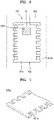
- FIG. 4 is a plan view of one pad terminal of FIG. 3 .
- a display apparatus 100 includes a display panel 110.
- the display apparatus 100 may be an organic light emitting display device (OLED).
- OLED organic light emitting display device
- the display apparatus 100 is not limited thereto and may be a liquid crystal display (LCD), a field emission display (FED), an electronic paper display (EPD), or any other form of display.
- LCD liquid crystal display
- FED field emission display
- EPD electronic paper display
- the display panel 110 includes a display substrate 120 having a plurality of devices and a thin film encapsulation (TFE) layer 130 disposed on the display substrate 120.
- TFE thin film encapsulation
- a plurality of thin film transistors (TFTs) and a plurality of light-emitting devices connected to the plurality of TFTs may be disposed on the display substrate 120.
- a functional film 140 such as a polarizing plate, a touch screen, or a cover window, may be disposed on the TFE layer 130.
- An active area AA 111 and an inactive area IAA 112 may be disposed on the display panel 110.
- the active area AA 111 may display an image.
- the inactive area IAA 112 may surround the active area AA 111.
- the TFE layer 130 may cover the active area AA 111.
- a bending area BA 413 in which the display panel 110 is foldable in one direction, may be disposed within the inactive area IAA 112.
- a pad area PA may extend beyond the bending area BA and may also be disposed within the inactive area IAA 112.
- exemplary embodiments of the present invention are not limited thereto, and the bending area BA may alternatively be formed within the active area AA 111.
- the case in which the bending area BA is formed within the inactive area IAA 112 will be described.
- the display panel 110 may be folded in one direction along a bending line BL that is within the bending area BA.
- exemplary embodiments of the present invention are not limited thereto, and the active area AA 111 and the pad area PA may be connected to each other without the existence of the bending area BA.
- the display panel 110 may also be rigid and no bending line BL might be present.
- the display panel 110 will be described herein as being foldable along the bending line BL.
- the pad area PA may be disposed at one edge of the display substrate 120.
- a plurality of pad terminals 150 may be disposed within the pad area PA.
- the plurality of pad terminals 150 may be spaced apart from each other in both the X-axis direction and the Y-axis direction of the display substrate 120.
- the pad terminals 150 may be connected to a wiring 113 that extends from the active area AA 111.
- the plurality of pad terminals 150 may be electrically connected to a driver 160.
- the driver 160 may include a driving circuit and the driver 160 may be a chip on plastic (COP).
- the driver 160 is not limited thereto.
- the driver 160 may be a chip on film (COF) or a chip on glass (COG).
- the driver 160 includes a flexible film 170 on which a circuit wiring is patterned, a driving integrated circuit (IC) 180 disposed on the display substrate 120, and a plurality of driving terminals 190 disposed under the driving IC 180.
- the flexible film 170 and the driving IC 180 may be electrically connected to each other, for example, via the display substrate 120.
- the flexible film 170 may be electrically connected to a circuit board 200.
- the circuit board 200 may be a flexible printed circuit board (FPCB).
- the pad terminals of the plurality of pad terminals 150 are electrically connected to corresponding driving terminals of the plurality of driving terminals 190.
- each of the plurality of pad terminals 150 may be directly connected to corresponding driving terminals.
- the plurality of pad terminals 150 may be connected to one another via a connection portion (see CP of FIG. 8 ).
- the connection portion CP is a layer that is formed by ultrasonic bonding the pad terminals 150 and the driving terminals 190 to each other. Part of the adjacent pad terminals 150 and part of the driving terminals 190 are diffused toward each other during the ultrasound bonding process and are thereby coupled to each other. A detailed coupling structure of the pad terminals 150 and the driving terminal 190 will be described below with reference to FIGS. 8 through 21 .
- FIG. 3 is a cross-sectional view of a display panel according to an exemplary embodiment of the present invention
- FIG. 4 is a plan view illustrating a pad terminal of FIG. 3 .
- a display panel 300 includes a display substrate 301 and a TFE layer 317.
- the display panel 300 may be an organic light emitting display (OLED) panel.
- a display area DA is disposed in the active area AA 111 of the display substrate 301 and a pad area PA is disposed in the inactive area IAA 112 of the display substrate 301.
- the display substrate 301 may be a flexible glass substrate, a flexible polymer substrate, a rigid glass substrate, or a rigid polymer substrate.
- the display substrate 301 may be transparent, semitransparent, or opaque.
- a barrier layer 302 may be disposed on the display substrate 301.
- the barrier layer 302 may cover a top surface of the display substrate 301.
- the barrier layer 302 may either be an organic layer or an inorganic layer.
- the barrier layer 302 may either include a single layer or may include multiple layers.
- At least one TFT may be disposed in the display area DA.
- a semiconductor active layer 303 may be disposed on the barrier layer 302.
- the semiconductor active layer 303 includes a source area 304 and a drain area 305, which may be formed by doping N-type impurity ions or P-type impurity ions into the semiconductor active layer 303.
- a channel region 306, into which no impurities are doped, may be formed between the source area 304 and the drain area 305.
- the semiconductor active layer 303 may include an organic semiconductor, an inorganic semiconductor, or amorphous silicon. According to an exemplary embodiment of the present invention, the semiconductor active layer 303 may include an oxide semiconductor.
- a gate insulating layer 307 may be deposited onto the semiconductor active layer 303.
- the gate insulating layer 307 may either be an organic layer or inorganic layer.
- the gate insulating layer 307 may include either a single layer or multiple layers.
- a gate electrode 308 may be disposed on the gate insulating layer 307.
- the gate electrode 308 may include an electrically conductive metal.
- the gate electrode 308 may include molybdenum (Mo), aluminum (Al), copper (Cu), and/or titanium (Ti).
- Mo molybdenum
- Al aluminum
- Cu copper
- Ti titanium
- the gate electrode 308 may include either a single layer or multiple layers.
- An interlayer insulating layer 309 may be disposed on the gate electrode 308.
- the interlayer insulating layer 309 may either be an organic layer or an inorganic layer.
- a source electrode 310 and a drain electrode 311 may be disposed on the interlayer insulating layer 309. Contact holes may be formed by removing part of the gate insulating layer 307 and part of the interlayer insulating layer 309.
- the source electrode 310 may be electrically connected to the source area 304 through one of the contact holes, and the drain electrode 311 may be electrically connected to the drain area 305 through another of the contact holes.
- the source electrode 310 and the drain electrode 311 may be formed of a conductive metal.
- the source electrode 310 and the drain electrode 311 may each include Mo, Al, Cu, and/or Ti.
- the source electrode 310 and the drain electrode 311 may each include either a single layer or multiple layers.
- the source electrode 310 and the drain electrode 311 may each have a structure in which Ti/AI/Ti are stacked.
- a protective layer 312 may be disposed on the source electrode 310 and the drain electrode 311.
- the protective layer 312 may either be an organic layer or inorganic layer.
- the protective layer 312 may be a passivation layer or a planarization layer. However, the passivation layer or the planarization layer may be omitted.
- the TFT may be electrically connected to the OLED.
- the OLED may be disposed on the protective layer 312.
- the OLED includes a first electrode 313, an intermediate layer 314, and a second electrode 315.
- the intermediate layer 314 may be disposed between the first and second electrodes 313 and 315.
- the first electrode 313 serves as an anode and may be formed of various conductive materials.
- the first electrode 313 may be either a transparent electrode or a reflective electrode.
- the first electrode 313 includes a transparent conductive layer.
- the first electrode 313 includes a reflective layer and a transparent conductive layer disposed on the reflective layer.
- the first electrode 313 may have a structure in which ITO/Ag/ITO are stacked.
- a pixel defining layer (PDL) 316 may be disposed on the protective layer 312.
- the PDL 316 may cover part of the first electrode 313.
- the PDL 316 may define an emission area of each of a plurality of sub-pixels by surrounding edges of the first electrode 313.
- the first electrode 313 may be patterned in each of the sub-pixels.
- the PDL 316 may either be an organic layer or an inorganic layer.
- the PDL 316 may include either a single layer or multiple layers.
- the intermediate layer 314 may be disposed in an area of the PDL 316 that has been exposed by etching.
- the intermediate layer 314 may be formed by a deposition process.
- the intermediate layer 314 may include an organic emission layer.
- the intermediate layer 314 includes a hole injection layer (HIL), a hole transport layer (HTL), an electron transport layer (ETL), and/or an electron injection layer (EIL), as well as an organic emission layer.
- HIL hole injection layer
- HTL hole transport layer
- ETL electron transport layer
- EIL electron injection layer
- the intermediate layer 314 may include an organic emission layer and may further include various other functional layers.
- the second electrode 315 may be disposed on the intermediate layer 314.
- the second electrode 315 may function as a cathode.
- the second electrode 315 may either be a transparent electrode or a reflective electrode.
- the second electrode 315 when the second electrode 315 is a transparent electrode, the second electrode 315 includes a metal layer and a transparent conductive layer disposed on the metal layer.
- the second electrode 315 when the second electrode 315 is a reflective electrode, the second electrode 315 includes a metal layer.
- a plurality of sub-pixels may be formed on the display substrate 301.
- red, green, and blue, or red, green, blue, and white sub-pixels may be included.
- embodiments of the present invention are not limited thereto.
- the TFE layer 317 may cover the OLED.
- First and second inorganic layers 318 and 319 and an organic layer 320 may be alternately stacked on the TFE layer 317.
- the first inorganic layer 318, the organic layer 320, and the second inorganic layer 319 may be sequentially stacked on the OLED.
- a touch screen 340 may be installed on the TFE layer 317.
- the touch screen 340 may be an electrostatic capacitive type touch screen.
- a base layer may be disposed on the TFE layer 317.
- a plurality of touch electrode wirings may be disposed on the base layer.
- the plurality of touch electrode wirings may have a structure in which Ti/AI/Ti are stacked.
- the base layer may be omitted.
- the touch electrode wirings may cover a touch electrode insulating layer.
- the touch electrode insulating layer may be an organic layer or an inorganic layer.
- a first insulating layer 331 may be disposed in the pad area PA of the display substrate 301.
- the first insulating layer 331 may be disposed on the same layer as the barrier layer 302.
- the first insulating layer 331 may be formed of the same material and by the same process as the barrier layer 302.
- a second insulating layer 332 may be disposed on the first insulating layer 331.
- the second insulating layer 331 may be disposed on the same layer as the gate insulating layer 307.
- the second insulating layer 332 may be formed of the same material and by the same process as the gate insulating layer 307.
- First conductive layers 410 disposed on each pad terminal 401 may be disposed on the second insulating layer 332 as each other.
- the first conductive layers 410 may be electrically connected to a wiring 325 that extends from the display area DA.
- the first conductive layers 410 may be disposed on the same layer as the gate electrode 308.
- each of the first conductive layers 410 may be formed of the same material and in the same process the gate electrode 308.
- the first conductive layers 410 may be spaced apart from one another in one direction of the display substrate 301.
- a third insulating layer 333 may be disposed on each of the first conductive layers 410.
- the third insulating layer 333 may be disposed on the same layer as the interlayer insulating layer 309.
- the third insulating layer 333 may be formed of the same material and in the same process as the interlayer insulating layer 309. According to an exemplary embodiment of the present invention, the third insulating layer 333 may either be an organic layer or an inorganic layer.
- the third insulating layer 333 may cover at least part of the first conductive layer 410. By removing part of the third insulating layer 333, a contact hole 431 may be formed in the first conductive layer 410. A top surface of the first conductive layer 410 may be exposed in a region of the first conductive layer 410 in which the contact hole 431 is formed.
- Second conductive layers 420 may be disposed on the first conductive layers 410.
- the second conductive layers 420 may be disposed in an island form on the first conductive layers 410.
- the second conductive layers 420 may be electrically connected to the wiring 325 that extends from the display area DA.
- the second conductive layers 420 may be disposed on the same layer as both the source electrode 310 and the drain electrode 311.
- the second conductive layer 420 may be formed of the same material and in the same process as the source electrode 310 and the drain electrode 311.
- the second conductive layers 420 may include a plurality of layers in which layers of Al and/or Ti are stacked.
- the stack structure of the second conductive layer 420 may be differently composed, for example, the second conductive layer 420 may include stacked layers such as Al/Ti/Al or Ti/AI/Ti.
- the second conductive layer 420 may be electrically connected to the first conductive layer 410 via the contact hole 431.
- the second conductive layer 420 may be electrically connected to the first conductive layer 410 in a region in the third insulating layer 333 is not disposed.
- the first conductive layer 410 and the second conductive layer 420 may form a contact portion CNT in a region in which the contact hole 431 is formed.
- the second conductive layer 420 may extend over a region of the first conductive layer 410 exposed through the contact hole 431 of FIG. 4 and the second conductive layer 420 may extend partially over the third insulating layer 333 where the third insulating layer 333 covers the first conductive layer 410 (e.g., as shown in FIG. 8 ).
- the size of the second conductive layer 420 may be greater than the size of the first conductive layer 410.
- the second conductive layer 420 may have the size sufficiently long so as to entirely cover the first conductive layer 410.
- the first conductive layer 410 and the second conductive layer 420 might not be electrically connected to each other in all regions but rather, they may be connected to each other through the contact hole 431 where part of the third insulating layer 333 is removed.
- Part of the second conductive layer 420 may be disposed in the exposed region of the first conductive layer 410 through the contact hole 431, and another part of the second conductive layer 420 may be disposed on the third insulating layer 333.
- each of the driving terminals 540 may be electrically connected to a corresponding pad terminal 401 (see FIG. 8 ).
- a circuit pattern 520 may be disposed under a driving IC 510.
- An insulating layer 530 may cover part of the circuit pattern 520.
- Each of the driving terminals 540 may be electrically connected to the circuit pattern 520.
- Each of the driving terminals 540 includes a bump.
- the driving terminal 540 may include gold (Au), nickel (Ni), and/or tin (Sn).
- Each of the driving terminals 540 may extend to a region in which the first conductive layer 410 and the second conductive layer 420 of FIG. 8 are electrically connected to each other and each of the driving terminals 540 may extend to a region in which the first conductive layer 410 and the second conductive layer 420 of FIG. 10 are spaced apart from each other and the third insulating layer 333 is disposed therebetween.
- the first conductive layer 410 and the second conductive layer 420 may be disposed on the same layers as other metal layers disposed on the display substrate 301 of FIG. 3 .
- These other metal layers may include the first electrode 313, the second electrode 315, and/or the touch electrode 322, as well as the gate electrode 308, the source electrode 310, and/or the drain electrode 311.
- the third insulating layer 333 may be disposed on the same layer as an insulating layer, such as the gate insulating layer 307, the protective layer 312, the PDL 316, the TFE layer 317, and/or the touch electrode insulating layers 323 and 324, which are patterned on the display substrate 301 of FIG. 3 , as well as the interlayer insulating layer 309.
- an insulating layer such as the gate insulating layer 307, the protective layer 312, the PDL 316, the TFE layer 317, and/or the touch electrode insulating layers 323 and 324, which are patterned on the display substrate 301 of FIG. 3 , as well as the interlayer insulating layer 309.
- FIG. 5 is a perspective view of part of the pad terminal of FIG. 4 .
- FIG. 6 is a plan view of one modified example of the pad terminal of FIG. 4 .
- FIG. 7 is a perspective view of part of the pad terminal of FIG. 6 .
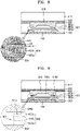
- FIG. 8 is a cross-sectional view taken along line A-A of FIG. 4 , which shows a driving terminal connected onto the pad terminal.
- FIG. 9 is a cross-sectional view taken along line B-B of FIG. 4 , which shows the driving terminal connected to the pad terminal.
- FIG. 10 is a cross-sectional view taken along line C-C of FIG. 4 , which shows the driving terminal connected to the pad terminal.
- FIG. 11 is a cross-sectional view of one modified example of FIG. 9 .
- FIG. 12 is a cross-sectional view of the pressurized driving terminal and pad terminal of FIG. 11 .
- a plurality of pad terminals 400 may be disposed in the pad area PA and may be electrically connected to the driving terminal 540.
- Each pad terminal 401 of the plurality of pad terminals 400 may be spaced apart from one another in one direction of the display substrate 301.
- each pad terminal 401 may include either a stepped groove 421a partially penetrating a surface facing each of the driving terminals 540 or an opening hole 421b that fully penetrates each pad terminal 401.
- a stepped groove 421a partially penetrating a surface facing each of the driving terminals 540
- an opening hole 421b that fully penetrates each pad terminal 401.
- FIGS. 4 and 5 only the stepped groove 421a is shown as being formed in each pad terminal 401, and in FIGS. 6 and 7 , only the opening hole 421b is shown as being formed in each pad terminal 401.
- each pad terminal 401 may include both the stepped groove 421a and the opening hole 421b.
- each pad terminal 401 and the driving terminal 540 may be electrically connected to each other via the connection portion CP. As described above, each pad terminal 401 and the driving terminal 540 may be coupled to each other by performing ultrasound bonding. Through ultrasound bonding, surfaces on which each pad terminal 401 and the driving terminal 540 contact each other may be softened and diffused and thus the surfaces may be coupled to each other.
- connection portion CP may be formed as a mixed layer in which part of each pad terminal 401 and part of the driving terminal 540 are mixed with each other.
- each pad terminal 401 is formed of Ti
- the driving terminal 540 is formed of Au
- ultrasound bonding may create a connection portion CP that includes both Ti and Au.
- a plurality of stepped grooves 421a and a plurality of opening holes 421b may be formed on the entire surface of each pad terminal 401. At least part of the plurality of stepped grooves 421a and the plurality of opening holes 421b may be shielded by the connection portion CP.
- each pad terminal 401 and the driving terminal 540 are connected to each other using ultrasound bonding.
- ultrasound bonding may be performed on part of the driving terminal 540 when the part of the driving terminal 540 is inserted into the stepped groove 421a or the opening hole 421b of each pad terminal 401.
- the connection portion CP formed by connecting each pad terminal 401 and the driving terminal 540 using ultrasound bonding may shield part of the stepped groove 421a or the opening hole 421b.
- the stepped groove 421a or the opening hole 421b may be formed in a region in which each pad terminal 401 and the driving terminal 540 do not contact each other.
- the stepped groove 421a and the opening hole 421b might not be shielded by the connection portion CP but, rather, may remain exposed.
- each pad terminal 401 of the plurality of pad terminals 400 may include a first conductive layer 410 and a plurality of second conductive layers 420 (including 420a, 420b, and 420c).
- the plurality of second conductive layers 420 is disposed on the first conductive layer 410.
- three, second conductive layers 420a, 420b, and 420c are shown in the drawings, the second conductive layers 420 may alternatively be formed as a single layer.
- the second conductive layers 420a, 420b and 420c are formed as a single second conductive layer 420, and a structure in which the second conductive layer 420 is coupled to the driving terminal 540, will be described.
- At least part of the first conductive layer 410 and at least part of the second conductive layer 420 may be electrically connected to each other.
- the stepped groove 421a and the opening hole 421b of each pad terminal 401 may be formed in the second conductive layer 420.
- the stepped groove 421a and the opening hole 421b may be formed within one of the plurality of second conductive layers 420a, 420b, and 420c at an upper side facing the driving terminal 540.
- the driving terminal 540 illustrated in FIGS. 8 through 12 may include a protrusion portion 540p that protrudes toward each pad terminal 401 at an edge of one surface of the driving terminal 540 facing each pad terminal 401.
- the protrusion portion 540p may contact the respective pad terminal 401 and a concave portion 540c that is inserted in a direction opposite to a direction toward each pad terminal 401 in the center of the driving terminal 540 and spaced apart from the respective pad terminal 401.
- the protrusion portion 540p of the driving terminal 540 may be formed in the center of the driving terminal 540, and alternatively, the concave portion 540c may be formed at an edge of one surface of the driving terminal 540 facing each pad terminal 401. This configuration will be described in greater detail below with reference to FIGS. 13 through 15 .
- connection portion (CP of FIG. 8 ) may be formed at the edge of the driving terminal 540 of each pad terminal 401.
- At least part of the stepped groove (421a of FIG. 9 ) and at least part of the opening hole (421b of FIG. 11 ) may also be formed at edges of each pad terminal 401 and the driving terminal 540.
- connection portion CP is shown in FIG. 8.
- FIGS. 9 and 11 show a state before each pad terminal 401 and the driving terminal 540 are ultrasonic-bonded, and therefore, before the connection portion CP is formed.
- a process in which the connection portion CP is formed will be described in detail below with reference to FIG. 12 .
- FIG. 12 illustrates part of a process of manufacturing the display apparatus 100 in which each pad terminal 401 and the driving terminal 540 are coupled to each other.
- FIG. 12 shows a state after a process of forming an opening hole 421b in the second conductive layer 420 of each pad terminal 401 has been performed, and a state in which each pad terminal 401 and the driving terminal 540 contact each other and are pressurized in a first direction (a direction of arrows) in which each pad terminal 401 and the driving terminal 540 are close to each other. Pressure may be applied to bring each pad terminal 401 into close contact with the driving terminal 540.
- the opening hole 421b may be formed in the driving terminal 540, as shown in FIGS. 16 through 19 , as well as in each pad terminal 401. Also, as illustrated in FIGS. 20 and 21 , the opening hole 421b may be formed in each pad terminal 401 and in the driving terminal 540. Also, the stepped groove 421a of FIG. 9 , as well as the opening hole 421b, may also be formed in each pad terminal 401 and/or the driving terminal 540.
- each pad terminal 401 and the driving terminal 540 are coupled to each other will be described based on a case where the opening hole 421b is formed in only the second conductive layer 420 of each pad terminal 401.
- each pad terminal 401 and the driving terminal 540 are pressurized in the first direction (see arrows) in which each pad terminal 401 and the driving terminal 540 are close to each other, part of the driving terminal 540 may be inserted into the opening hole 421b of the second conductive layer 420.
- the driving terminal 540 may be moved lower than a shape of the driving terminal 540 before being pressurized (see the X-axis of FIG. 12 ). This is because part of the driving terminal 540 may be inserted into a space of the opening hole 421b.
- each pad terminal 401 and the driving terminal 540 may be vibrated in a second direction that crosses the first direction (for example, the first direction may be a width direction and the second direction may be a height directions of FIG. 4 ). Also, each pad terminal 401 and the driving terminal 540 may be electrically coupled to each other using an ultrasound bonding process.
- connection portion CP may be formed thereby.
- the connection portion CP may be formed to fully fill the opening hole 421b.
- the connection portion CP may be formed to only partially fill the opening hole 421b so that the connection portion CP may have a structure for shielding the opening hole 421b from the outside.
- each pad terminal 401 and the driving terminal 540 are connected to each other using ultrasound bonding, a slip phenomenon may occur at an interface between each pad terminal 401 and the driving terminal 540.
- a slip phenomenon may occur at the interface between each pad terminal 401 and the driving terminal 540.
- each pad terminal 401 might not be properly aligned with the driving terminal 540 and a connection defect in which each pad terminal 401 and the driving terminal 540 are not electrically connected to each other, may occur.
- each pad terminal 401 and the driving terminal 540 may be vibrated when part of the driving terminal 540 is inserted into the stepped groove 421a or the opening hole 421b formed in each pad terminal 401 such that friction between each pad terminal 401 and the driving terminal 540 may be maximized.
- FIG. 13 is a cross-sectional view of a modified example of FIG. 10 .
- FIG. 14 is a cross-sectional view of a modified example of FIG. 10 .
- FIG. 15 is a cross-sectional view of a modified example of FIG. 10 .
- the protrusion portion 540p of the driving terminal 540 may also be formed in the center of the driving terminal 540, as described above.
- a connection portion may be formed in the center of each pad terminal 401 and the driving terminal 540, and at least part of the stepped groove 421a and the opening hole 421b may also be formed in the center of each pad terminal 401 and the driving terminal 540.
- the stepped groove 421a may be formed in the center of the second conductive layer 420 of each pad terminal 401 that contacts the protrusion portion 540p.
- the opening hole 421b may also be formed in the center of the second conductive layer 420 of each pad terminal 401 that contacts the protrusion portion 540p.
- the opening hole 421b may also be formed in the center of the second conductive layer 420 of each pad terminal 401 that contacts the protrusion portion 540p.
- the stepped groove 421a and the opening hole 421b may also be formed in the driving terminal 540, as well as in each pad terminal 401. This structure will be described below with reference to FIGS. 16 through 19 .
- FIG. 16 is a cross-sectional view of a modified example of FIG. 9 .
- FIG. 17 is a cross-sectional view of a modified example of FIG. 9 .
- FIG. 18 is a cross-sectional view of a modified example of FIG. 10 .
- FIG. 19 is a cross-sectional view of a modified example of FIG. 10 .
- the protrusion portion 540p of the driving terminal 540 may be formed at an edge of one surface of the driving terminal 540 that faces each pad terminal 401.
- a stepped groove 541a may be formed in the protrusion portion 540p.
- the stepped groove 541a shown in FIG. 16 is not enlarged, as shown in FIG. 9 .
- the stepped groove 541a may be formed in part of the protrusion portion 540p, and the other part of the protrusion portion 540p may contact the second conductive layer 420 of each pad terminal 401.
- an opening hole 541b may also be formed in the protrusion portion 540p at the edge of one surface of the driving terminal 540 that faces each pad terminal 401.
- part of the second conductive layer 420 may be inserted into the opening hole 541b.
- the ultrasound bonding process is performed so that a connection portion may be formed to electrically connect each pad terminal 401 to the driving terminal 540.
- the protrusion portion 540p of the driving terminal 540 may also be formed in the center of the driving terminal 540.
- the stepped groove 541a may be formed in the protrusion portion 540p in the center of the driving terminal 540.
- the opening hole 541b may also be formed in the protrusion portion 540p formed in the center of the driving terminal 540.
- the stepped groove 421a and the opening hole 421b may be simultaneously formed in each pad terminal 401 and the driving terminal 540. This structure will be descried below with reference to FIGS. 20 and 21 .
- FIG. 20 is a cross-sectional view of a modified example of FIG. 10
- FIG. 21 is a cross-sectional view of a modified example of FIG. 10 .
- a second stepped groove 541a may be formed in the protrusion portion 540p at the edge of one surface of the driving terminal 540 that faces each pad terminal 401, and simultaneously, a first stepped groove 421a may be formed in the second conductive layer 420 of each pad terminal 401 that contacts the protrusion portion 540p.
- a first stepped groove 421a and the second stepped groove 541a may be disposed to project in opposite directions with respect to each other.
- each pad terminal 401 and the driving terminal 540 when the ultrasound bonding process of each pad terminal 401 and the driving terminal 540 is performed, due to pressure applied to each pad terminal 401 and the driving terminal 540, part of each pad terminal 401 may be inserted into the second stepped groove 541a formed in the driving terminal 540, and simultaneously, part of the driving terminal 540 may be inserted into the first stepped groove 421a formed in each pad terminal 401. In this state, the ultrasound bonding process may be performed to form a connection portion electrically connecting each pad terminal 401 and the driving terminal 540.
- a second opening hole 541b may be formed in the protrusion portion 540p at the edge of one surface of the driving terminal 540 that faces each pad terminal 401, and simultaneously, a first opening hole 421b may be formed in the second conductive layer 420 of each pad terminal 401 that contacts the protrusion portion 540p.
- the first opening hole 421b and the second opening hole 541b may be disposed to project in opposite directions.
- each pad terminal 401 and the driving terminal 540 when the ultrasound bonding process of each pad terminal 401 and the driving terminal 540 is performed, due to pressure applied to each pad terminal 401 and the driving terminal 540, part of each pad terminal 401 may be inserted into the second opening hole 541b formed in the driving terminal 540, and simultaneously, part of the driving terminal 540 may be inserted into the first opening hole 421b formed in each pad terminal 401. In this state, the ultrasound bonding process may be performed so that a connection portion may be formed to electrically connect each pad terminal 401 to the driving terminal 540.
- the center of the driving terminal 540 may also be formed as a concave portion 540c, and the edge of one surface of the driving terminal 540 that faces each pad terminal 401 may also be formed as the protrusion portion 540p.
- embodiments of the present invention are not limited thereto.
- one or both of the stepped groove 421a and the opening hole 421b may be formed in the center of each pad terminal 401.
- one or both of the stepped groove 541a and the opening hole 541b may also be formed in a protrusion portion (not shown) of the driving terminal 540.
- second conductive layers 1420 and 2420 of each pad terminal 1400 will be described with reference to FIGS. 22 and 23 .
- FIG. 22 is a plan view of a modified example of each pad terminal 401 of FIG. 4
- FIG. 23 is a plan view of a modified example of each pad terminal 401 of FIG. 4 .
- the second conductive layer 1420 of each pad terminal 1400 may include a plurality of circular opening holes 1421.
- FIG. 22 shows the opening holes 1421 that pass through the second conductive layer 1420.
- the opening holes 1421 may also be formed as stepped grooves 1421 spaced apart from a surface facing the driving terminal 540 by a predetermined distance.
- part of the driving terminal 540 that contacts the second conductive layer 1420 may be inserted into each of the opening holes 1421.
- the pad terminal 1400 and the driving terminal are engaged with each other so that friction between the pad terminal 1400 and the driving terminal 540 may be maximized and slipping may be minimized.
- the second conductive layer 2420 of a pad terminal 2400 may also include a plurality of opening holes 2421 formed in both sides of the second conductive layer 2420 at a particular angle of inclination.
- FIG. 23 shows the opening holes 2421 that pass through the second conductive layer 2420, as in FIG. 22 .
- Embodiments of the present invention are not limited to this particular structure.
- the opening holes 2421 may also be formed as stepped grooves 2421 spaced apart from a surface facing the driving terminal 540 by a predetermined distance.
- part of the driving terminal 540 that contacts the second conductive layer 1420 may be inserted into the opening holes 2421.
- a frictional force between the pad terminal 1400 and the driving terminal 540 may be maximized.
- a slip phenomenon that may occur between the pad terminal 1400 and the driving terminal 540 may be minimized.
- the second conductive layers 1420 and 2420 of the pad terminals 1400 and 2400 illustrated in FIGS. 22 and 23 may be formed in various shapes. Some of these shapes are shown in the drawings and some are not. As described above, at least one stepped groove, at least one opening hole 1421, or at least one opening hole 2421 may be formed in a surface facing the driving terminal 540 of each of the second conductive layers 1420 and 2420. In this configuration, a frictional force between the driving terminal 540 and the pad terminal 400 may be optimized for the ultrasound bonding process of coupling the driving terminal 540 to the pad terminal 400.
- a display apparatus in which a pad terminal and a driving terminal can be electrically stably coupled to each other is provided. Additionally, a method of manufacturing the same can be implemented.
- An exemplary embodiment of the invention concerns an electronic device including a display apparatus, the display apparatus comprising: a display panel including at least one pad terminal disposed thereon; a display driver including at least one driving terminal disposed thereon, the driving terminal being connected to the pad terminal; a first cutout in the pad terminal or a second cutout in the driving terminal; and a connection portion disposed between the pad terminal and the driving terminal, the connection portion including a mixing of a first material from the pad terminal and a second material from the driving terminal.
- the first cutout can penetrate the pad terminal only partly or fully and/or the second cutout can penetrate the driving terminal only partly or fully.
- the first protrusion and/or the second protrusion can have a trapezoidal cross-section.
Landscapes
- Engineering & Computer Science (AREA)
- Physics & Mathematics (AREA)
- Microelectronics & Electronic Packaging (AREA)
- Manufacturing & Machinery (AREA)
- Nonlinear Science (AREA)
- Optics & Photonics (AREA)
- Mathematical Physics (AREA)
- Chemical & Material Sciences (AREA)
- Crystallography & Structural Chemistry (AREA)
- General Physics & Mathematics (AREA)
- Electroluminescent Light Sources (AREA)
- Devices For Indicating Variable Information By Combining Individual Elements (AREA)
Claims (13)
- Eine Anzeigevorrichtung (100), die Folgendes umfasst:eine Anzeigetafel (110) mit einem Anzeigesubstrat (120),eine Vielzahl von Pad-Anschlüssen (150, 401, 1400), die auf dem Anzeigesubstrat (120) angeordnet sind; undeine Antriebseinheit (160) mit einer Vielzahl von Antriebsanschlüssen (190, 540), die elektrisch mit der Vielzahl von Pad-Anschlüssen (150, 401, 1400) verbunden sind,wobei jeder der mehreren Pad-Anschlüsse (150, 401, 1400) eine erste abgestufte Nut (421a) aufweist, die einem entsprechenden Antriebsanschluss der mehreren Antriebsanschlüsse (190, 540) gegenüberliegt, oder jeder der mehreren Pad-Anschlüsse (150, 401, 1400) ein erstes Öffnungsloch (1421, 2421, 421b) aufweist, das dem entsprechenden Antriebsanschluss der mehreren Antriebsanschlüsse (190, 540) gegenüberliegt, dadurch gekennzeichnet, dass,jeder der Vielzahl von Antriebsanschlüssen (540) umfasst:
einen Vorsprungsabschnitt (540p), der in einer ersten Richtung vorsteht, die zu dem entsprechenden aus der Vielzahl von Pad-Anschlüssen (401) gerichtet ist und den entsprechenden aus der Vielzahl von Pad-Anschlüssen (401) berührt; und
einen konkaven Abschnitt (540c), der in einer zweiten Richtung entgegengesetzt zur ersten Richtung und beabstandet von dem entsprechenden der Vielzahl von Pad-Anschlüssen (401) angeordnet ist. - Anzeigevorrichtung nach Anspruch 1, die ferner einen Verbindungsabschnitt (CP) umfasst, der jeden der mehreren Pad-Anschlüsse (150) mit dem entsprechenden der mehreren Treiberanschlüsse (190) elektrisch verbindet, wobei der Verbindungsabschnitt (CP) ein Gemisch aus einem ersten Material von den Pad-Anschlüssen (150) und einem zweiten Material von den Treiberanschlüssen (190) enthält.
- Anzeigevorrichtung nach Anspruch 2, wobei jeder der mehreren Pad-Anschlüsse (150) ferner mehrere mehrere erste abgestufte Rillen einschließlich der ersten abgestuften Rille (421a) und mehrere erste Öffnungslöcher einschließlich des ersten Öffnungslochs (1421, 2421, 421b) umfasst,
wobei zumindest ein Teil der Mehrzahl von abgestuften Nuten oder zumindest ein Teil der Mehrzahl von ersten Öffnungslöchern durch den Verbindungsabschnitt (CP) abgeschirmt ist. - Anzeigevorrichtung nach einem der Ansprüche 1 bis 3, wobei der vorstehende Abschnitt (540p) an einer Kante einer Oberfläche jedes der mehreren Antriebsanschlüsse (540) angeordnet ist, die dem entsprechenden der mehreren Pad-Anschlüsse (401) zugewandt ist, und der konkave Abschnitt (540c) in einer Mitte jedes der mehreren Antriebsanschlüsse (540) angeordnet ist.
- Anzeigevorrichtung nach einem der Ansprüche 3 oder 4, wenn sie von Anspruch 3 abhängt, wobei zumindest ein Teil der ersten Mehrzahl von gestuften Rillen und zumindest ein Teil der Mehrzahl von ersten Öffnungslöchern an einer Kante einer Oberfläche jedes der Mehrzahl von Pad-Anschlüssen (401) angeordnet ist, die dem entsprechenden der Mehrzahl von Antriebsanschlüssen (540) zugewandt ist.
- Anzeigevorrichtung nach einem der Ansprüche 1 bis 3 oder 5, wenn Anspruch 5 nur von Anspruch 3 abhängt, wobei der vorstehende Abschnitt (540p) in einer Mitte jedes der mehreren Antriebsanschlüsse (540) angeordnet ist und der konkave Abschnitt (540c) an einer Kante einer Oberfläche jedes der mehreren Antriebsanschlüsse (540) angeordnet ist, die dem entsprechenden der mehreren Polsteranschlüsse (401) zugewandt ist.
- Anzeigevorrichtung nach einem der Ansprüche 3, 5 oder 6, wenn Anspruch 5 nur von Anspruch 3 abhängt, wobei mindestens ein Teil jeder der mehreren ersten gestuften Rillen und mindestens ein Teil jedes der mehreren ersten Öffnungslöcher in der Mitte jedes der mehreren Pad-Anschlüsse (401) angeordnet sind.
- Anzeigevorrichtung nach einem der vorangehenden Ansprüche, ferner umfassend:eine Dünnfilm-Verkapselungsschicht (TFE) (317), die auf dem Anzeigesubstrat (120) angeordnet ist; undwobei jeder der mehreren Antriebsanschlüsse (540) eine zweite abgestufte Nut (541a) aufweist, die den entsprechenden der mehreren Antriebsanschlüsse (540) teilweise durchdringt, oder ein zweites Öffnungsloch (541b), das den entsprechenden der mehreren Antriebsanschlüsse (540) vollständig durchdringt.
- Anzeigevorrichtung nach Anspruch 8, wobei die erste gestufte Nut (421a) und die zweite gestufte Nut (541a) ihre jeweiligen Anschlüsse in entgegengesetzten Richtungen voneinander durchdringen und das erste Öffnungsloch (421b) und das zweite Öffnungsloch (541b) ihre jeweiligen Anschlüsse in entgegengesetzten Richtungen durchdringen.
- Anzeigevorrichtung nach einem der Ansprüche 8 und 9, wenn beide Ansprüche von Anspruch 2 abhängen, wobei jeder der mehreren Pad-Anschlüsse (150) ferner mehrere zweite abgestufte Rillen, einschließlich des ersten Öffnungslochs, und mehrere zweite Öffnungslöcher, einschließlich des zweiten Öffnungslochs, aufweist,
wobei zumindest ein Teil der Mehrzahl von ersten gestuften Nuten, zumindest ein Teil der Mehrzahl von zweiten gestuften Nuten, zumindest ein Teil der Mehrzahl von ersten Öffnungslöchern oder zumindest ein Teil der Mehrzahl von zweiten Öffnungslöchern durch den Verbindungsabschnitt (CP) abgeschirmt sind. - Anzeigevorrichtung nach Anspruch 10, wenn Anspruch 10 von Anspruch 4 abhängt, wobei mindestens ein Teil der mehreren ersten gestuften Rillen und mindestens ein Teil der mehreren ersten Öffnungslöcher an einer Kante einer Oberfläche jedes der mehreren Pad-Anschlüsse (401) angeordnet sind, die dem entsprechenden der mehreren Treiberanschlüsse (540) zugewandt ist, und zumindest ein Teil der Mehrzahl von zweiten abgestuften Nuten und zumindest ein Teil der Mehrzahl von zweiten Öffnungslöchern an einer Kante einer Oberfläche von jedem der Mehrzahl von Antriebsanschlüssen (540) angeordnet sind, die dem entsprechenden der Mehrzahl von Pad-Anschlüssen (401) zugewandt ist.
- Anzeigevorrichtung nach einem der Ansprüche 10 oder 11, wenn die Ansprüche 10 und 11 von Anspruch 4 abhängen, wobei mindestens ein Teil der mehreren ersten abgestuften Nuten und mindestens ein Teil der mehreren ersten Öffnungslöcher in der Mitte jedes der mehreren Pad-Anschlüsse (401) angeordnet sind und mindestens ein Teil der mehreren zweiten abgestuften Nuten und mindestens ein Teil der mehreren zweiten Öffnungslöcher in der Mitte jedes der mehreren Antriebsanschlüsse (540) angeordnet sind.
- Elektronisches Gerät mit einer Anzeigevorrichtung (100) nach einem der vorhergehenden Ansprüche, wobei die Anzeigevorrichtung umfasst:
eine erste Aussparung in der Anschlussklemme (401) oder eine zweite Aussparung in der Antriebsklemme (540).
Applications Claiming Priority (2)
| Application Number | Priority Date | Filing Date | Title |
|---|---|---|---|
| KR1020160077556A KR102654925B1 (ko) | 2016-06-21 | 2016-06-21 | 디스플레이 장치 및 이의 제조 방법 |
| EP17176523.3A EP3260912B1 (de) | 2016-06-21 | 2017-06-19 | Anzeigevorrichtung mit gerillten anschlüssen und verfahren zur herstellung davon |
Related Parent Applications (2)
| Application Number | Title | Priority Date | Filing Date |
|---|---|---|---|
| EP17176523.3A Division EP3260912B1 (de) | 2016-06-21 | 2017-06-19 | Anzeigevorrichtung mit gerillten anschlüssen und verfahren zur herstellung davon |
| EP17176523.3A Division-Into EP3260912B1 (de) | 2016-06-21 | 2017-06-19 | Anzeigevorrichtung mit gerillten anschlüssen und verfahren zur herstellung davon |
Publications (2)
| Publication Number | Publication Date |
|---|---|
| EP3663845A1 EP3663845A1 (de) | 2020-06-10 |
| EP3663845B1 true EP3663845B1 (de) | 2022-10-19 |
Family
ID=59152645
Family Applications (2)
| Application Number | Title | Priority Date | Filing Date |
|---|---|---|---|
| EP20152740.5A Active EP3663845B1 (de) | 2016-06-21 | 2017-06-19 | Anzeigevorrichtung mit gerillten anschlüssen |
| EP17176523.3A Active EP3260912B1 (de) | 2016-06-21 | 2017-06-19 | Anzeigevorrichtung mit gerillten anschlüssen und verfahren zur herstellung davon |
Family Applications After (1)
| Application Number | Title | Priority Date | Filing Date |
|---|---|---|---|
| EP17176523.3A Active EP3260912B1 (de) | 2016-06-21 | 2017-06-19 | Anzeigevorrichtung mit gerillten anschlüssen und verfahren zur herstellung davon |
Country Status (4)
| Country | Link |
|---|---|
| US (4) | US10217806B2 (de) |
| EP (2) | EP3663845B1 (de) |
| KR (1) | KR102654925B1 (de) |
| CN (1) | CN107527937B (de) |
Families Citing this family (26)
| Publication number | Priority date | Publication date | Assignee | Title |
|---|---|---|---|---|
| KR102654925B1 (ko) | 2016-06-21 | 2024-04-05 | 삼성디스플레이 주식회사 | 디스플레이 장치 및 이의 제조 방법 |
| KR102373440B1 (ko) * | 2017-03-17 | 2022-03-14 | 삼성디스플레이 주식회사 | 디스플레이 패널 및 이를 구비하는 디스플레이 장치 |
| WO2019026280A1 (ja) * | 2017-08-04 | 2019-02-07 | シャープ株式会社 | 樹脂基板および表示デバイス |
| KR102511074B1 (ko) | 2018-05-10 | 2023-03-16 | 삼성디스플레이 주식회사 | 표시 장치 |
| KR102533660B1 (ko) | 2018-07-04 | 2023-05-17 | 삼성디스플레이 주식회사 | 표시 장치 |
| KR102603403B1 (ko) | 2018-08-09 | 2023-11-17 | 삼성디스플레이 주식회사 | 표시 장치 |
| KR102657249B1 (ko) * | 2018-08-27 | 2024-04-15 | 삼성디스플레이 주식회사 | 표시 패널, 및 이를 포함하는 표시 장치 |
| CN109213391B (zh) * | 2018-09-25 | 2020-11-17 | 京东方科技集团股份有限公司 | 一种触控显示面板及其制作方法、显示装置 |
| KR102778880B1 (ko) * | 2019-03-13 | 2025-03-10 | 삼성디스플레이 주식회사 | 표시 장치 |
| KR102833789B1 (ko) | 2019-03-21 | 2025-07-15 | 삼성디스플레이 주식회사 | 표시 장치 및 이의 제조 방법 |
| CN109949703B (zh) * | 2019-03-26 | 2021-08-06 | 京东方科技集团股份有限公司 | 柔性显示基板、显示面板、显示装置及制作方法 |
| KR102769361B1 (ko) | 2019-04-01 | 2025-02-17 | 삼성디스플레이 주식회사 | 표시 장치 및 그 제조 방법 |
| CN109935601B (zh) | 2019-04-04 | 2021-01-26 | 京东方科技集团股份有限公司 | 一种显示面板及其制备方法 |
| KR20200145877A (ko) * | 2019-06-19 | 2020-12-31 | 삼성디스플레이 주식회사 | 표시 장치, 칩온 필름의 제조 장치, 및 칩온 필름의 제조 방법 |
| KR102843099B1 (ko) | 2019-07-12 | 2025-08-06 | 삼성디스플레이 주식회사 | 표시 장치 및 표시 장치의 제조 방법 |
| KR20210011529A (ko) * | 2019-07-22 | 2021-02-02 | 삼성디스플레이 주식회사 | 표시 장치 및 표시 장치의 제조 방법 |
| KR102911249B1 (ko) * | 2019-08-07 | 2026-01-14 | 삼성디스플레이 주식회사 | 표시장치 및 이의 제조 방법 |
| KR102796654B1 (ko) * | 2019-09-02 | 2025-04-16 | 삼성디스플레이 주식회사 | 표시 장치 |
| KR102909642B1 (ko) | 2020-02-20 | 2026-01-09 | 삼성디스플레이 주식회사 | 표시 장치 및 이의 제조 방법 |
| US11322720B2 (en) * | 2020-02-27 | 2022-05-03 | Wuhan China Star Optoelectronics Semiconductor Display Technology Co., Ltd. | Display panel having a grooved non-display area |
| KR102920188B1 (ko) | 2020-06-01 | 2026-02-02 | 삼성디스플레이 주식회사 | 표시장치 및 이의 제조 방법 |
| KR102914370B1 (ko) | 2020-06-01 | 2026-01-20 | 삼성디스플레이 주식회사 | 표시장치 및 이의 제조 방법 |
| KR20220014405A (ko) * | 2020-07-24 | 2022-02-07 | 삼성디스플레이 주식회사 | 디스플레이 장치 |
| WO2022176772A1 (ja) * | 2021-02-18 | 2022-08-25 | ソニーセミコンダクタソリューションズ株式会社 | ディスプレイモジュールおよびその製造方法、ならびに電子機器 |
| KR20230131332A (ko) | 2022-03-03 | 2023-09-13 | 삼성디스플레이 주식회사 | 표시 장치, 이의 제조 방법 및 이를 포함하는 타일형 표시 장치 |
| TWI839970B (zh) * | 2022-11-25 | 2024-04-21 | 友達光電股份有限公司 | 電子裝置 |
Family Cites Families (63)
| Publication number | Priority date | Publication date | Assignee | Title |
|---|---|---|---|---|
| US4293637A (en) * | 1977-05-31 | 1981-10-06 | Matsushita Electric Industrial Co., Ltd. | Method of making metal electrode of semiconductor device |
| JPH0917824A (ja) * | 1995-06-30 | 1997-01-17 | Toshiba Corp | 電子回路装置およびその製造方法 |
| US5834354A (en) | 1996-11-07 | 1998-11-10 | Advanced Micro Devices, Inc. | Ultra high density NOR gate using a stacked transistor arrangement |
| KR100307385B1 (ko) | 1997-03-05 | 2001-12-15 | 구본준, 론 위라하디락사 | 액정표시장치의구조및그제조방법 |
| JP3767154B2 (ja) * | 1997-06-17 | 2006-04-19 | セイコーエプソン株式会社 | 電気光学装置用基板、電気光学装置、電子機器及び投写型表示装置 |
| US6259119B1 (en) * | 1997-12-18 | 2001-07-10 | Lg. Philips Lcd Co, Ltd. | Liquid crystal display and method of manufacturing the same |
| KR100341840B1 (ko) * | 1999-12-16 | 2002-06-24 | 구자홍 | 플라즈마 디스플레이 패널의 격벽 성형장치 및 그 펀치 가공장치 |
| JP2002373779A (ja) * | 2001-06-13 | 2002-12-26 | Sony Corp | 電気的接続装置および電気的接続装置を有する電子機器 |
| US7297572B2 (en) * | 2001-09-07 | 2007-11-20 | Hynix Semiconductor, Inc. | Fabrication method for electronic system modules |
| KR100417916B1 (ko) | 2001-12-29 | 2004-02-14 | 엘지.필립스 엘시디 주식회사 | 액정표시장치용 어레이 기판 |
| TWI245402B (en) * | 2002-01-07 | 2005-12-11 | Megic Corp | Rod soldering structure and manufacturing process thereof |
| JP4104489B2 (ja) * | 2002-05-17 | 2008-06-18 | 東芝松下ディスプレイテクノロジー株式会社 | 表示装置及びその製造方法 |
| JP4095518B2 (ja) * | 2002-10-31 | 2008-06-04 | セイコーエプソン株式会社 | 電気光学装置及び電子機器 |
| US7192812B2 (en) * | 2002-12-20 | 2007-03-20 | Seiko Epson Corporation | Method for manufacturing electro-optical substrate |
| US20040178165A1 (en) | 2003-03-12 | 2004-09-16 | Konefal Robert S. | Closure and container package with child-resistant and non-child-resistant modes of operation |
| JP2005166950A (ja) | 2003-12-02 | 2005-06-23 | Sumitomo Precision Prod Co Ltd | プラズマ発生器及びプラズマエッチング装置 |
| JP2005166960A (ja) | 2003-12-03 | 2005-06-23 | Matsushita Electric Ind Co Ltd | 半導体装置およびその製造方法 |
| KR20050093606A (ko) * | 2004-03-20 | 2005-09-23 | 삼성에스디아이 주식회사 | 전계 발광 디스플레이 장치 및 이의 제조 방법 |
| US7687402B2 (en) | 2004-11-15 | 2010-03-30 | Micron Technology, Inc. | Methods of making optoelectronic devices, and methods of making solar cells |
| KR20060072767A (ko) * | 2004-12-23 | 2006-06-28 | 엘지.필립스 엘시디 주식회사 | 액정표시소자 |
| US20060206828A1 (en) | 2005-03-11 | 2006-09-14 | Kinpo Electronics, Inc. | Display device of a calculator capable of displaying a composite icon |
| JP4327220B2 (ja) * | 2005-07-26 | 2009-09-09 | 東北パイオニア株式会社 | 表示装置の検査方法 |
| KR101134168B1 (ko) | 2005-08-24 | 2012-04-09 | 삼성전자주식회사 | 반도체 칩 및 그 제조 방법과, 그를 이용한 표시 패널 및그 제조 방법 |
| KR100671643B1 (ko) * | 2006-01-27 | 2007-01-19 | 삼성에스디아이 주식회사 | 유기전계발광 표시 장치 및 그의 제조 방법 |
| KR100741131B1 (ko) * | 2006-06-20 | 2007-07-19 | 삼성에스디아이 주식회사 | 플라즈마 표시장치 |
| KR100818451B1 (ko) * | 2006-07-03 | 2008-04-01 | 삼성전기주식회사 | 편광성을 갖는 반도체 발광 소자 |
| KR100812001B1 (ko) * | 2006-11-10 | 2008-03-10 | 삼성에스디아이 주식회사 | 유기전계발광 표시장치 및 그 제조방법 |
| SG155096A1 (en) | 2008-03-03 | 2009-09-30 | Micron Technology Inc | Board-on-chip type substrates with conductive traces in multiple planes, semiconductor device packages including such substrates, and associated methods |
| JP2008160168A (ja) * | 2008-03-26 | 2008-07-10 | Seiko Epson Corp | 半導体装置及びその製造方法 |
| US7671436B2 (en) * | 2008-05-02 | 2010-03-02 | Agere Systems Inc. | Electronic packages |
| KR100952824B1 (ko) * | 2008-06-18 | 2010-04-15 | 삼성모바일디스플레이주식회사 | 유기전계발광 표시장치 |
| JP2010019896A (ja) * | 2008-07-08 | 2010-01-28 | Canon Inc | 画像表示装置 |
| US8665192B2 (en) | 2009-07-08 | 2014-03-04 | Hitachi Displays, Ltd. | Liquid crystal display device |
| JP5585013B2 (ja) * | 2009-07-14 | 2014-09-10 | 日亜化学工業株式会社 | 発光装置 |
| US8203134B2 (en) * | 2009-09-21 | 2012-06-19 | Micron Technology, Inc. | Memory devices with enhanced isolation of memory cells, systems including same and methods of forming same |
| KR101084256B1 (ko) * | 2009-12-08 | 2011-11-16 | 삼성모바일디스플레이주식회사 | 유기 발광 표시 장치 및 이의 제조 방법 |
| US8288230B2 (en) | 2010-09-30 | 2012-10-16 | Infineon Technologies Austria Ag | Method for producing a gate electrode structure |
| US8669137B2 (en) * | 2011-04-01 | 2014-03-11 | International Business Machines Corporation | Copper post solder bumps on substrate |
| US8409979B2 (en) * | 2011-05-31 | 2013-04-02 | Stats Chippac, Ltd. | Semiconductor device and method of forming interconnect structure with conductive pads having expanded interconnect surface area for enhanced interconnection properties |
| US8643196B2 (en) * | 2011-07-27 | 2014-02-04 | Taiwan Semiconductor Manufacturing Company, Ltd. | Structure and method for bump to landing trace ratio |
| KR20130013515A (ko) * | 2011-07-28 | 2013-02-06 | 삼성디스플레이 주식회사 | 유기 발광 표시 장치 |
| JP6033071B2 (ja) * | 2011-12-23 | 2016-11-30 | 株式会社半導体エネルギー研究所 | 半導体装置 |
| KR101942918B1 (ko) * | 2012-05-03 | 2019-01-28 | 삼성전자주식회사 | 칩 온 필름 패키지 및 이를 포함하는 장치 어셈블리 |
| US20130292819A1 (en) * | 2012-05-07 | 2013-11-07 | Novatek Microelectronics Corp. | Chip-on-film device |
| KR101495713B1 (ko) | 2012-05-07 | 2015-02-25 | 노바텍 마이크로일렉트로닉스 코포레이션 | 칩온필름 장치 |
| US9257197B2 (en) | 2012-07-06 | 2016-02-09 | Micron Technology, Inc. | Apparatuses and/or methods for operating a memory cell as an anti-fuse |
| US8828860B2 (en) * | 2012-08-30 | 2014-09-09 | International Business Machines Corporation | Double solder bumps on substrates for low temperature flip chip bonding |
| WO2014093266A1 (en) | 2012-12-10 | 2014-06-19 | Key Safety Systems Inc. | A seat belt buckle presenter assembly |
| DE102013212331A1 (de) | 2013-04-04 | 2014-10-09 | Telsonic Holding Ag | Verfahren zum Verbinden eines Rohrkabelschuhs mit einer aus Aluminium hergestellten Litze |
| KR20150003587A (ko) * | 2013-07-01 | 2015-01-09 | 삼성디스플레이 주식회사 | 표시 장치 및 그 제조 방법 |
| DE102013214285A1 (de) | 2013-07-22 | 2015-01-22 | Siemens Aktiengesellschaft | Verwendung mehrerer TX-Spulen |
| US9778531B2 (en) * | 2013-07-29 | 2017-10-03 | Chromogenics Ab | Contacting of electrochromic devices |
| KR20150072467A (ko) * | 2013-12-19 | 2015-06-30 | 주성엔지니어링(주) | 터치패널 제조 장치, 시스템 및 방법 |
| KR102212323B1 (ko) | 2014-02-10 | 2021-02-04 | 삼성디스플레이 주식회사 | 표시 장치 |
| KR102215881B1 (ko) * | 2014-02-17 | 2021-02-17 | 삼성디스플레이 주식회사 | 테이프 패키지 및 이를 포함하는 표시 장치 |
| JP2015169760A (ja) | 2014-03-06 | 2015-09-28 | 株式会社ジャパンディスプレイ | 表示装置の製造方法、表示装置および表示装置形成基板 |
| JP2015200753A (ja) | 2014-04-07 | 2015-11-12 | 株式会社ジャパンディスプレイ | 表示装置 |
| US9478779B2 (en) | 2014-08-20 | 2016-10-25 | Ford Global Technologies, Llc | Cell to cell terminal connections for a high voltage battery |
| CN204287637U (zh) * | 2014-11-19 | 2015-04-22 | 上海天马微电子有限公司 | 阵列基板、显示面板和显示装置 |
| US10242968B2 (en) * | 2015-11-05 | 2019-03-26 | Massachusetts Institute Of Technology | Interconnect structure and semiconductor structures for assembly of cryogenic electronic packages |
| JP6700027B2 (ja) * | 2015-11-20 | 2020-05-27 | スタンレー電気株式会社 | 垂直共振器型発光素子 |
| US9868630B2 (en) * | 2016-05-20 | 2018-01-16 | Taiwan Semiconductor Manufacturing Co., Ltd. | Package structure and manufacturing method thereof |
| KR102654925B1 (ko) | 2016-06-21 | 2024-04-05 | 삼성디스플레이 주식회사 | 디스플레이 장치 및 이의 제조 방법 |
-
2016
- 2016-06-21 KR KR1020160077556A patent/KR102654925B1/ko active Active
- 2016-11-28 US US15/362,082 patent/US10217806B2/en active Active
-
2017
- 2017-06-19 EP EP20152740.5A patent/EP3663845B1/de active Active
- 2017-06-19 EP EP17176523.3A patent/EP3260912B1/de active Active
- 2017-06-21 CN CN201710474301.1A patent/CN107527937B/zh active Active
-
2019
- 2019-02-04 US US16/267,003 patent/US10879335B2/en active Active
-
2020
- 2020-12-08 US US17/115,744 patent/US11605697B2/en active Active
-
2023
- 2023-01-31 US US18/162,136 patent/US11997901B2/en active Active
Also Published As
| Publication number | Publication date |
|---|---|
| KR102654925B1 (ko) | 2024-04-05 |
| KR20180000046A (ko) | 2018-01-02 |
| EP3663845A1 (de) | 2020-06-10 |
| US20230172021A1 (en) | 2023-06-01 |
| EP3260912B1 (de) | 2020-02-26 |
| US10879335B2 (en) | 2020-12-29 |
| US20170365653A1 (en) | 2017-12-21 |
| EP3260912A1 (de) | 2017-12-27 |
| CN107527937A (zh) | 2017-12-29 |
| CN107527937B (zh) | 2023-06-02 |
| US11605697B2 (en) | 2023-03-14 |
| US10217806B2 (en) | 2019-02-26 |
| US20210118973A1 (en) | 2021-04-22 |
| US20190172896A1 (en) | 2019-06-06 |
| US11997901B2 (en) | 2024-05-28 |
Similar Documents
| Publication | Publication Date | Title |
|---|---|---|
| US11997901B2 (en) | Display apparatus having grooved terminals | |
| US10741789B2 (en) | Flexible display device | |
| CN107068710B (zh) | 柔性显示设备 | |
| US10510821B2 (en) | Display device | |
| KR102421578B1 (ko) | 플렉서블 디스플레이 장치 | |
| US10748853B2 (en) | Flexible display device | |
| US11171194B2 (en) | Display apparatus | |
| KR102322766B1 (ko) | 디스플레이 장치 | |
| US12501800B2 (en) | Display device | |
| US20240381698A1 (en) | Display device and method of manufacturing the same | |
| KR20250098054A (ko) | 표시 장치 및 그의 제조 방법 | |
| KR20250129840A (ko) | 표시 장치 및 이의 제조 방법 | |
| KR20240126926A (ko) | 표시 장치 및 표시 장치의 제조 방법 |
Legal Events
| Date | Code | Title | Description |
|---|---|---|---|
| PUAI | Public reference made under article 153(3) epc to a published international application that has entered the european phase |
Free format text: ORIGINAL CODE: 0009012 |
|
| STAA | Information on the status of an ep patent application or granted ep patent |
Free format text: STATUS: THE APPLICATION HAS BEEN PUBLISHED |
|
| AC | Divisional application: reference to earlier application |
Ref document number: 3260912 Country of ref document: EP Kind code of ref document: P |
|
| AK | Designated contracting states |
Kind code of ref document: A1 Designated state(s): AL AT BE BG CH CY CZ DE DK EE ES FI FR GB GR HR HU IE IS IT LI LT LU LV MC MK MT NL NO PL PT RO RS SE SI SK SM TR |
|
| STAA | Information on the status of an ep patent application or granted ep patent |
Free format text: STATUS: REQUEST FOR EXAMINATION WAS MADE |
|
| 17P | Request for examination filed |
Effective date: 20201209 |
|
| RBV | Designated contracting states (corrected) |
Designated state(s): AL AT BE BG CH CY CZ DE DK EE ES FI FR GB GR HR HU IE IS IT LI LT LU LV MC MK MT NL NO PL PT RO RS SE SI SK SM TR |
|
| GRAP | Despatch of communication of intention to grant a patent |
Free format text: ORIGINAL CODE: EPIDOSNIGR1 |
|
| STAA | Information on the status of an ep patent application or granted ep patent |
Free format text: STATUS: GRANT OF PATENT IS INTENDED |
|
| INTG | Intention to grant announced |
Effective date: 20220602 |
|
| GRAS | Grant fee paid |
Free format text: ORIGINAL CODE: EPIDOSNIGR3 |
|
| GRAA | (expected) grant |
Free format text: ORIGINAL CODE: 0009210 |
|
| STAA | Information on the status of an ep patent application or granted ep patent |
Free format text: STATUS: THE PATENT HAS BEEN GRANTED |
|
| AC | Divisional application: reference to earlier application |
Ref document number: 3260912 Country of ref document: EP Kind code of ref document: P |
|
| AK | Designated contracting states |
Kind code of ref document: B1 Designated state(s): AL AT BE BG CH CY CZ DE DK EE ES FI FR GB GR HR HU IE IS IT LI LT LU LV MC MK MT NL NO PL PT RO RS SE SI SK SM TR |
|
| REG | Reference to a national code |
Ref country code: GB Ref legal event code: FG4D |
|
| REG | Reference to a national code |
Ref country code: CH Ref legal event code: EP |
|
| REG | Reference to a national code |
Ref country code: IE Ref legal event code: FG4D |
|
| REG | Reference to a national code |
Ref country code: DE Ref legal event code: R096 Ref document number: 602017062920 Country of ref document: DE |
|
| REG | Reference to a national code |
Ref country code: AT Ref legal event code: REF Ref document number: 1525919 Country of ref document: AT Kind code of ref document: T Effective date: 20221115 |
|
| REG | Reference to a national code |
Ref country code: LT Ref legal event code: MG9D |
|
| REG | Reference to a national code |
Ref country code: NL Ref legal event code: MP Effective date: 20221019 |
|
| REG | Reference to a national code |
Ref country code: AT Ref legal event code: MK05 Ref document number: 1525919 Country of ref document: AT Kind code of ref document: T Effective date: 20221019 |
|
| PG25 | Lapsed in a contracting state [announced via postgrant information from national office to epo] |
Ref country code: NL Free format text: LAPSE BECAUSE OF FAILURE TO SUBMIT A TRANSLATION OF THE DESCRIPTION OR TO PAY THE FEE WITHIN THE PRESCRIBED TIME-LIMIT Effective date: 20221019 |
|
| PG25 | Lapsed in a contracting state [announced via postgrant information from national office to epo] |
Ref country code: SE Free format text: LAPSE BECAUSE OF FAILURE TO SUBMIT A TRANSLATION OF THE DESCRIPTION OR TO PAY THE FEE WITHIN THE PRESCRIBED TIME-LIMIT Effective date: 20221019 Ref country code: PT Free format text: LAPSE BECAUSE OF FAILURE TO SUBMIT A TRANSLATION OF THE DESCRIPTION OR TO PAY THE FEE WITHIN THE PRESCRIBED TIME-LIMIT Effective date: 20230220 Ref country code: NO Free format text: LAPSE BECAUSE OF FAILURE TO SUBMIT A TRANSLATION OF THE DESCRIPTION OR TO PAY THE FEE WITHIN THE PRESCRIBED TIME-LIMIT Effective date: 20230119 Ref country code: LT Free format text: LAPSE BECAUSE OF FAILURE TO SUBMIT A TRANSLATION OF THE DESCRIPTION OR TO PAY THE FEE WITHIN THE PRESCRIBED TIME-LIMIT Effective date: 20221019 Ref country code: FI Free format text: LAPSE BECAUSE OF FAILURE TO SUBMIT A TRANSLATION OF THE DESCRIPTION OR TO PAY THE FEE WITHIN THE PRESCRIBED TIME-LIMIT Effective date: 20221019 Ref country code: ES Free format text: LAPSE BECAUSE OF FAILURE TO SUBMIT A TRANSLATION OF THE DESCRIPTION OR TO PAY THE FEE WITHIN THE PRESCRIBED TIME-LIMIT Effective date: 20221019 Ref country code: AT Free format text: LAPSE BECAUSE OF FAILURE TO SUBMIT A TRANSLATION OF THE DESCRIPTION OR TO PAY THE FEE WITHIN THE PRESCRIBED TIME-LIMIT Effective date: 20221019 |
|
| PG25 | Lapsed in a contracting state [announced via postgrant information from national office to epo] |
Ref country code: RS Free format text: LAPSE BECAUSE OF FAILURE TO SUBMIT A TRANSLATION OF THE DESCRIPTION OR TO PAY THE FEE WITHIN THE PRESCRIBED TIME-LIMIT Effective date: 20221019 Ref country code: PL Free format text: LAPSE BECAUSE OF FAILURE TO SUBMIT A TRANSLATION OF THE DESCRIPTION OR TO PAY THE FEE WITHIN THE PRESCRIBED TIME-LIMIT Effective date: 20221019 Ref country code: LV Free format text: LAPSE BECAUSE OF FAILURE TO SUBMIT A TRANSLATION OF THE DESCRIPTION OR TO PAY THE FEE WITHIN THE PRESCRIBED TIME-LIMIT Effective date: 20221019 Ref country code: IS Free format text: LAPSE BECAUSE OF FAILURE TO SUBMIT A TRANSLATION OF THE DESCRIPTION OR TO PAY THE FEE WITHIN THE PRESCRIBED TIME-LIMIT Effective date: 20230219 Ref country code: HR Free format text: LAPSE BECAUSE OF FAILURE TO SUBMIT A TRANSLATION OF THE DESCRIPTION OR TO PAY THE FEE WITHIN THE PRESCRIBED TIME-LIMIT Effective date: 20221019 Ref country code: GR Free format text: LAPSE BECAUSE OF FAILURE TO SUBMIT A TRANSLATION OF THE DESCRIPTION OR TO PAY THE FEE WITHIN THE PRESCRIBED TIME-LIMIT Effective date: 20230120 |
|
| P01 | Opt-out of the competence of the unified patent court (upc) registered |
Effective date: 20230516 |
|
| REG | Reference to a national code |
Ref country code: DE Ref legal event code: R097 Ref document number: 602017062920 Country of ref document: DE |
|
| PG25 | Lapsed in a contracting state [announced via postgrant information from national office to epo] |
Ref country code: SM Free format text: LAPSE BECAUSE OF FAILURE TO SUBMIT A TRANSLATION OF THE DESCRIPTION OR TO PAY THE FEE WITHIN THE PRESCRIBED TIME-LIMIT Effective date: 20221019 Ref country code: RO Free format text: LAPSE BECAUSE OF FAILURE TO SUBMIT A TRANSLATION OF THE DESCRIPTION OR TO PAY THE FEE WITHIN THE PRESCRIBED TIME-LIMIT Effective date: 20221019 Ref country code: EE Free format text: LAPSE BECAUSE OF FAILURE TO SUBMIT A TRANSLATION OF THE DESCRIPTION OR TO PAY THE FEE WITHIN THE PRESCRIBED TIME-LIMIT Effective date: 20221019 Ref country code: DK Free format text: LAPSE BECAUSE OF FAILURE TO SUBMIT A TRANSLATION OF THE DESCRIPTION OR TO PAY THE FEE WITHIN THE PRESCRIBED TIME-LIMIT Effective date: 20221019 Ref country code: CZ Free format text: LAPSE BECAUSE OF FAILURE TO SUBMIT A TRANSLATION OF THE DESCRIPTION OR TO PAY THE FEE WITHIN THE PRESCRIBED TIME-LIMIT Effective date: 20221019 |
|
| PLBE | No opposition filed within time limit |
Free format text: ORIGINAL CODE: 0009261 |
|
| STAA | Information on the status of an ep patent application or granted ep patent |
Free format text: STATUS: NO OPPOSITION FILED WITHIN TIME LIMIT |
|
| PG25 | Lapsed in a contracting state [announced via postgrant information from national office to epo] |
Ref country code: SK Free format text: LAPSE BECAUSE OF FAILURE TO SUBMIT A TRANSLATION OF THE DESCRIPTION OR TO PAY THE FEE WITHIN THE PRESCRIBED TIME-LIMIT Effective date: 20221019 Ref country code: AL Free format text: LAPSE BECAUSE OF FAILURE TO SUBMIT A TRANSLATION OF THE DESCRIPTION OR TO PAY THE FEE WITHIN THE PRESCRIBED TIME-LIMIT Effective date: 20221019 |
|
| 26N | No opposition filed |
Effective date: 20230720 |
|
| PG25 | Lapsed in a contracting state [announced via postgrant information from national office to epo] |
Ref country code: SI Free format text: LAPSE BECAUSE OF FAILURE TO SUBMIT A TRANSLATION OF THE DESCRIPTION OR TO PAY THE FEE WITHIN THE PRESCRIBED TIME-LIMIT Effective date: 20221019 |
|
| PG25 | Lapsed in a contracting state [announced via postgrant information from national office to epo] |
Ref country code: MC Free format text: LAPSE BECAUSE OF FAILURE TO SUBMIT A TRANSLATION OF THE DESCRIPTION OR TO PAY THE FEE WITHIN THE PRESCRIBED TIME-LIMIT Effective date: 20221019 |
|
| PG25 | Lapsed in a contracting state [announced via postgrant information from national office to epo] |
Ref country code: MC Free format text: LAPSE BECAUSE OF FAILURE TO SUBMIT A TRANSLATION OF THE DESCRIPTION OR TO PAY THE FEE WITHIN THE PRESCRIBED TIME-LIMIT Effective date: 20221019 |
|
| REG | Reference to a national code |
Ref country code: CH Ref legal event code: PL |
|
| REG | Reference to a national code |
Ref country code: BE Ref legal event code: MM Effective date: 20230630 |
|
| PG25 | Lapsed in a contracting state [announced via postgrant information from national office to epo] |
Ref country code: LU Free format text: LAPSE BECAUSE OF NON-PAYMENT OF DUE FEES Effective date: 20230619 |
|
| REG | Reference to a national code |
Ref country code: IE Ref legal event code: MM4A |
|
| PG25 | Lapsed in a contracting state [announced via postgrant information from national office to epo] |
Ref country code: LU Free format text: LAPSE BECAUSE OF NON-PAYMENT OF DUE FEES Effective date: 20230619 |
|
| PG25 | Lapsed in a contracting state [announced via postgrant information from national office to epo] |
Ref country code: IE Free format text: LAPSE BECAUSE OF NON-PAYMENT OF DUE FEES Effective date: 20230619 |
|
| PG25 | Lapsed in a contracting state [announced via postgrant information from national office to epo] |
Ref country code: IE Free format text: LAPSE BECAUSE OF NON-PAYMENT OF DUE FEES Effective date: 20230619 Ref country code: CH Free format text: LAPSE BECAUSE OF NON-PAYMENT OF DUE FEES Effective date: 20230630 |
|
| PG25 | Lapsed in a contracting state [announced via postgrant information from national office to epo] |
Ref country code: IT Free format text: LAPSE BECAUSE OF FAILURE TO SUBMIT A TRANSLATION OF THE DESCRIPTION OR TO PAY THE FEE WITHIN THE PRESCRIBED TIME-LIMIT Effective date: 20221019 Ref country code: BE Free format text: LAPSE BECAUSE OF NON-PAYMENT OF DUE FEES Effective date: 20230630 |
|
| PG25 | Lapsed in a contracting state [announced via postgrant information from national office to epo] |
Ref country code: BG Free format text: LAPSE BECAUSE OF FAILURE TO SUBMIT A TRANSLATION OF THE DESCRIPTION OR TO PAY THE FEE WITHIN THE PRESCRIBED TIME-LIMIT Effective date: 20221019 |
|
| PG25 | Lapsed in a contracting state [announced via postgrant information from national office to epo] |
Ref country code: BG Free format text: LAPSE BECAUSE OF FAILURE TO SUBMIT A TRANSLATION OF THE DESCRIPTION OR TO PAY THE FEE WITHIN THE PRESCRIBED TIME-LIMIT Effective date: 20221019 |
|
| PGFP | Annual fee paid to national office [announced via postgrant information from national office to epo] |
Ref country code: DE Payment date: 20250520 Year of fee payment: 9 |
|
| PGFP | Annual fee paid to national office [announced via postgrant information from national office to epo] |
Ref country code: GB Payment date: 20250520 Year of fee payment: 9 |
|
| PGFP | Annual fee paid to national office [announced via postgrant information from national office to epo] |
Ref country code: FR Payment date: 20250521 Year of fee payment: 9 |
|
| PG25 | Lapsed in a contracting state [announced via postgrant information from national office to epo] |
Ref country code: CY Free format text: LAPSE BECAUSE OF FAILURE TO SUBMIT A TRANSLATION OF THE DESCRIPTION OR TO PAY THE FEE WITHIN THE PRESCRIBED TIME-LIMIT; INVALID AB INITIO Effective date: 20170619 |
|
| PG25 | Lapsed in a contracting state [announced via postgrant information from national office to epo] |
Ref country code: HU Free format text: LAPSE BECAUSE OF FAILURE TO SUBMIT A TRANSLATION OF THE DESCRIPTION OR TO PAY THE FEE WITHIN THE PRESCRIBED TIME-LIMIT; INVALID AB INITIO Effective date: 20170619 |
|
| PG25 | Lapsed in a contracting state [announced via postgrant information from national office to epo] |
Ref country code: TR Free format text: LAPSE BECAUSE OF FAILURE TO SUBMIT A TRANSLATION OF THE DESCRIPTION OR TO PAY THE FEE WITHIN THE PRESCRIBED TIME-LIMIT Effective date: 20221019 |