EP3652524B1 - Device and process for detecting surface defects - Google Patents
Device and process for detecting surface defects Download PDFInfo
- Publication number
- EP3652524B1 EP3652524B1 EP18749871.2A EP18749871A EP3652524B1 EP 3652524 B1 EP3652524 B1 EP 3652524B1 EP 18749871 A EP18749871 A EP 18749871A EP 3652524 B1 EP3652524 B1 EP 3652524B1
- Authority
- EP
- European Patent Office
- Prior art keywords
- electromagnetic radiation
- intensity
- band
- inspected
- spectral
- Prior art date
- Legal status (The legal status is an assumption and is not a legal conclusion. Google has not performed a legal analysis and makes no representation as to the accuracy of the status listed.)
- Active
Links
Images
Classifications
-
- G—PHYSICS
- G01—MEASURING; TESTING
- G01B—MEASURING LENGTH, THICKNESS OR SIMILAR LINEAR DIMENSIONS; MEASURING ANGLES; MEASURING AREAS; MEASURING IRREGULARITIES OF SURFACES OR CONTOURS
- G01B11/00—Measuring arrangements characterised by the use of optical techniques
- G01B11/24—Measuring arrangements characterised by the use of optical techniques for measuring contours or curvatures
- G01B11/25—Measuring arrangements characterised by the use of optical techniques for measuring contours or curvatures by projecting a pattern, e.g. one or more lines, moiré fringes on the object
-
- G—PHYSICS
- G01—MEASURING; TESTING
- G01N—INVESTIGATING OR ANALYSING MATERIALS BY DETERMINING THEIR CHEMICAL OR PHYSICAL PROPERTIES
- G01N21/00—Investigating or analysing materials by the use of optical means, i.e. using sub-millimetre waves, infrared, visible or ultraviolet light
- G01N21/84—Systems specially adapted for particular applications
- G01N21/88—Investigating the presence of flaws or contamination
- G01N21/8806—Specially adapted optical and illumination features
- G01N2021/8829—Shadow projection or structured background, e.g. for deflectometry
Definitions
- the present invention relates to devices and methods for detecting surface defects, specifically on painted surfaces, according to the preamble of the independent claims.
- the painted surfaces specifically the painted surfaces of metal components in the automotive field, have very high quality standards: a small painting defect has to be detected before the part is assembled and leaves the factory .
- the defects of painted surfaces, or however of surfaces being subjected to surface treatment comprise clots of paint or resin, dust or impurities that blended with the paint or resin.
- defects are three-dimensional, i.e. they are not simply local color variations, but ridges or however irregularities on the surface.
- defects also comprise defects such as bumps or lines being on the surface even before the painting operation or also a missed surface cleaning which can result in a paint ripple.
- a light source projecting a plurality of light and dark parallel lines on the surface to be inspected is used.
- a localized defect reflects the light in a different way and can thus be visualized as a sudden irregularity of the lines reflected by the test surface.
- the deflectometry requires glossy and highly reflective surfaces, since the surface roughness increases the light diffusion in all the directions and decreases the specular reflection.
- JPH05322543 (A ) improvements to increase the reliability of the technique have been proposed.
- a video camera can capture the images reflected by the surface to be inspected and mathematical algorithms can allow an automated analysis thereof.
- WO 2008/123604 A1 describes an apparatus and a method for detecting a defect on a surface using a diffuse light source.
- US 2014/043602 A1 further describes a device for applying both the fringe pattern method and deflectormetry on a surface to be inspected.
- US 2008/0204733 A1 describes a device for the detection of meat discoloration and bones in chicken breast fillets, in which a first polarizing filter is placed in front of a light source and a second polarizing filter is placed in front of an imaging device.
- deflectometry requires an accurate positioning of the video camera with respect to the light source and the surface to be inspected.
- Another issue is that the detection of the defects depends on the color of the paint and the condition thereof.
- a defect such as for example an orange peel effect painted surface, can hardly be detected by current techniques.
- Object of the present invention is therefore to realize a device and a process which allow overcoming the mentioned drawbacks .
- an object is to realize a device and a process for detecting defects on the surface of elements to be inspected, in particular on painted surfaces, which increases the reliability of the technique and the likelihood of detecting the defect.
- Another object is to realize a device and a process for detecting defects on painted elements, which works on all colors .
- Another object is to obtain a device simpler than the current ones, with larger freedom of positioning the components.
- the human eye visible electromagnetic radiation ranges from about 400 nm (purple) to 750 nm (red) .
- the not-visible radiation beyond the red is named as infrared radiation.
- the infrared radiation is categorized in non-thermal infrared (from 750 nm to about 2000 nm) and thermal infrared (beyond 2000 nm) .
- a body being at room temperature (about 300 K) emits infrared radiation in the thermal infrared band, but not in the non-thermal infrared band, and thus under 2000 nm.
- Normal video cameras with CCD or CMOS sensor are sensitive in the 300 nm - 1100 nm band and can thus see in the non-thermal infrared region to which the human eye is not sensitive.
- This property is used to see in the dark, by using an infrared illuminator, for example a suitable led.
- an infrared source emits infrared radiation which is reflected by an object and then captured by the sensor of a video camera, such as in the visible.
- the room temperature bodies emit electromagnetic radiation and such emitted radiation is added to the possibly reflected radiation.
- the radiation emitted by a source and addressed to a surface to be inspected, is partly specularly reflected by the surface and partly and diffusely reflected in all the directions.
- the share of radiation diffusely reflected in all the directions increases as the surface roughness of the surface to be inspected increases.
- the deflectometric techniques are based on the radiation specularly reflected by the surface to be inspected, the radiation diffusely reflected in all the directions can allow detecting surface and painting defects with a better signal-to-noise ratio and thus a better likelihood of correctly detecting the defect.
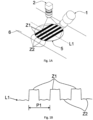
- the device according to the invention for detecting defects on surfaces to be inspected preferably painted surfaces, is shown, comprising
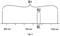
- the source 1 can be a normal incandescent lamp or a neon or led lamp or any other source, such as for example a laser, emitting in a spectral band B1 which overlaps at least partly to the spectral band B2 wherein the video camera is sensitive.
- the intersection between said first band B1 and said second band B2 establishes a spectral working band BL wherein the device is operative.
- One of the first and second bands B1 or B2 can be completely comprised in the other one, whereby the spectral working band BL corresponds to one of the two bands.
- the second band B2 wherein the video camera is sensitive is completely comprised in the first band B1 wherein the source emits, whereby the spectral working band BL is corresponding to the second band B2 of the video camera.
- Said spectral working band can also comprise several bands, for example one in the visible and one in the non- thermal infrared.
- the video camera can comprise a normal black and white video camera with CCD (charge coupled device) or CMOS (complementary metal-oxide semiconductor) sensor which is sensitive in a spectral band from 300 to 1100 nm, thus also comprising a part of non-thermal infrared, to which a filter is put before in order to select the desired spectral working band.
- CCD charge coupled device
- CMOS complementary metal-oxide semiconductor
- the spectral working band has a bandwidth lower than or equal to 200 nm and is between 300 nm and 1100 nm.
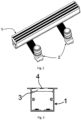
- the diffuser 3 can comprise an opaline or a milky semitransparent element interposed between the source 1 and the surface 6 to be inspected. While a normal lamp or light source lightens a surface with non-homogeneous intensity, the device according to the invention obtains better results when the intensity of the emitted electromagnetic radiation is homogeneously distributed over the surface to be inspected.
- the diffuser 3 helps to make more homogeneous the distribution of the intensity of the electromagnetic radiation emitted by the source 1.
- the spectral working band BL is adequately narrow and has therefore a bandwidth lower than or equal to 50 nm, even better if said spectral working band BL has a bandwidth lower than or equal to 20 nm.
- a spectral working band BL is arranged in the non-thermal infrared, for example if the spectral working band BL is between 750 nm and 1050 nm.
- spectral working band BL is between 810 nm and 860 nm.
- the currently existing devices often project onto the surface to be inspected a plurality of light and dark lines, which alternate a high light intensity and a low light intensity.
- the device according to the invention comprises an intensity alternator 4 adapted to intercept, after the diffuser 3, the electromagnetic radiation emitted by the source 1 and to generate, on said at least one surface to be inspected 6, a spatial arrangement 5 of the electromagnetic radiation comprising high-intensity electromagnetic radiation zones alternating with low- intensity electromagnetic radiation zones.
- such a spatial arrangement 5 of the intensity distribution of the electromagnetic radiation emitted by the source comprises a plurality of high-intensity electromagnetic radiation lines Z1 alternating with low-intensity electromagnetic radiation lines Z2, said lines Z1 and Z2 being substantially parallel.
- the alternation of high-intensity electromagnetic radiation lines Z1 with low- intensity electromagnetic radiation lines Z2 creates a repetitive figure, wherein the pitch PI (Fig. IB) of such a repetition is preferably small, lower than or equal to 20 mm, better if lower than or equal to 4 mm.
- the size of such a pitch PI also depends on the minimum size of the defect desired to be detected.
- the duty-cycle varies between 5% and 95%, i.e. that the thickness of the high-intensity electromagnetic radiation lines Z1 is different from that of the low-intensity electromagnetic radiation lines Z2, specifically that the thickness of the high- intensity electromagnetic radiation lines Z1 is smaller than that of the low-intensity electromagnetic radiation lines .
- the electromagnetic radiation emitted from the source is adequately diffused such that the passage from a high-intensity electromagnetic radiation zone to an adjacent low-intensity electromagnetic radiation zone is substantially stepped and the intensity of the electromagnetic radiation in the high-intensity electromagnetic radiation zone is homogeneous.
- the distribution of the electromagnetic radiation intensity over a line LI intersecting such high-intensity electromagnetic radiation zones (Zl) and low-intensity electromagnetic radiation zones (Z2) is preferably a substantially square wave function, with steep rising edge and falling edge and substantially uniform values in the high-intensity electromagnetic radiation zone Z1 and in the low-intensity electromagnetic radiation zone Z2.
- the ambient lightning can create a decrease in contrast and saturation and, if not arranged homogeneously, can determine a lower homogeneity of the radiation intensity.
- the video camera is preferred not to reach the saturation, when observing the high-intensity electromagnetic radiation zone Z1 on a defect-free surface to be inspected.
- the spectral working band may comprise two or more different spectral bands and the image acquisition may occur simultaneously on said spectral bands or in temporal succession (first on a band and then on another band).
- the images obtained on different bands are overlapped or processed together in accordance with convenient mathematical algorithms, in order to improve the signal- to-noise ratio and increase the likelihood of detecting possible defects being on the surface to be inspected.
- the relative position of the source and the video camera is not relevant.
- source 1 and video camera 2 are close together and mutually constrained.
- the video camera and the source are preferably arranged along a direction normal to the surface to be inspected. Such an arrangement is not usually adopted in the deflectometric techniques since, in order to obtain better sensitivity, it is preferred that the electromagnetic radiation emitted by the source impinge onto the surface to be inspected with an angle of at least 45° with respect to the normal, whereas the video camera is arranged in the specular direction with respect to the incidence direction of the electromagnetic radiation .
- the source 1 projects onto the surface to be inspected a beam of electromagnetic radiation having homogeneous high-intensity electromagnetic radiation zones alternating with low-intensity electromagnetic radiation zones, for example a strip spatial arrangement 5.
- the video camera 2 captures the surface to be inspected in the center portion of the beam projected by the source 1.
- the presence of a defect locally alters the homogeneity of the radiation intensity or locally deforms the spatial arrangement, thus allowing the defect to be detected.
- the defect can appear as low intensity spots in the high-intensity electromagnetic radiation zones and/or as high intensity spots in the low-intensity electromagnetic radiation zones, or as a distortion of the edges wherein the passage between a high-intensity electromagnetic radiation zone and a low-intensity electromagnetic radiation zone occurs.
- the surface to be inspected runs with respect to the device according to the invention such that the scan of the whole surface to be inspected can be obtained quickly .
- An electronic device for image analysis can easily and automatically detect the defects with high reliability.
- the present invention also provides a process for detecting surface irregularity defects on surfaces to be inspected, preferably on painted surfaces, comprising the following steps:
- the process comprises the image acquisition on different spectral working bands and the processing of said images by means of mathematical algorithms adapted to increase the signal-to-noise ratio and the likelihood of detecting a defect that might be on the surface to be inspected.
- the electromagnetic radiation being distributed homogeneously at least in the high-intensity electromagnetic radiation zones, the detection of the painting or geometric and aesthetic defects is made easier with respect to other today existing devices and the signal-to-noise ratio is improved, with higher reliability of the device.
- the inspection can of course be expected to be done in the visible spectrum by a human operator, thus without a video camera. However, in this case the corresponding method does not form part of the invention.
- the surfaces that can be inspected are not only painted surfaces, but also surfaces having been subjected or not to a surface treatment, such as resin deposition or even a transparent coating.
- the device according to the invention does not use an intensity alternator in order to have high-intensity electromagnetic radiation zones alternating with low- intensity electromagnetic radiation zones, but simply a diffuser in order to have an homogeneous distribution of the intensity of the electromagnetic radiation emitted by the source over the surface to be inspected.
- An adequate homogeneity of the electromagnetic radiation distribution over the surface to be inspected is often enough .
- An advantageous characteristic of the invention is that, conversely to the devices based on the deflectometric technique, the device according to the invention allows wide freedom in the arrangement of the video camera and the source.
Landscapes
- Physics & Mathematics (AREA)
- General Physics & Mathematics (AREA)
- Computer Vision & Pattern Recognition (AREA)
- Engineering & Computer Science (AREA)
- General Health & Medical Sciences (AREA)
- Biochemistry (AREA)
- Analytical Chemistry (AREA)
- Chemical & Material Sciences (AREA)
- Immunology (AREA)
- Pathology (AREA)
- Life Sciences & Earth Sciences (AREA)
- Health & Medical Sciences (AREA)
- Investigating Materials By The Use Of Optical Means Adapted For Particular Applications (AREA)
Applications Claiming Priority (2)
| Application Number | Priority Date | Filing Date | Title |
|---|---|---|---|
| IT102017000077459A IT201700077459A1 (it) | 2017-07-10 | 2017-07-10 | Dispositivo e procedimento per la rilevazione di difetti superficiali |
| PCT/IB2018/055041 WO2019012404A1 (en) | 2017-07-10 | 2018-07-09 | Device and process for detecting surface defects |
Publications (3)
| Publication Number | Publication Date |
|---|---|
| EP3652524A1 EP3652524A1 (en) | 2020-05-20 |
| EP3652524C0 EP3652524C0 (en) | 2024-02-14 |
| EP3652524B1 true EP3652524B1 (en) | 2024-02-14 |
Family
ID=61005905
Family Applications (1)
| Application Number | Title | Priority Date | Filing Date |
|---|---|---|---|
| EP18749871.2A Active EP3652524B1 (en) | 2017-07-10 | 2018-07-09 | Device and process for detecting surface defects |
Country Status (7)
| Country | Link |
|---|---|
| US (2) | US11105614B2 (enExample) |
| EP (1) | EP3652524B1 (enExample) |
| JP (2) | JP2020527728A (enExample) |
| ES (1) | ES2977710T3 (enExample) |
| IT (1) | IT201700077459A1 (enExample) |
| MA (1) | MA49568A (enExample) |
| WO (1) | WO2019012404A1 (enExample) |
Families Citing this family (3)
| Publication number | Priority date | Publication date | Assignee | Title |
|---|---|---|---|---|
| IT201700077459A1 (it) * | 2017-07-10 | 2019-01-10 | Tekno Idea Srl | Dispositivo e procedimento per la rilevazione di difetti superficiali |
| CN111189854B (zh) * | 2020-04-13 | 2020-08-07 | 征图新视(江苏)科技股份有限公司 | 玻璃盖板自动检测系统缺陷分层检测方法 |
| US12175654B2 (en) | 2020-11-06 | 2024-12-24 | Carl Zeiss Metrology Llc | Surface inspection system and method for differentiating particulate contamination from defects on a surface of a specimen |
Citations (1)
| Publication number | Priority date | Publication date | Assignee | Title |
|---|---|---|---|---|
| US20080204733A1 (en) * | 2005-01-12 | 2008-08-28 | Gareth Jones | Sensing in Meat Products and the Like |
Family Cites Families (21)
| Publication number | Priority date | Publication date | Assignee | Title |
|---|---|---|---|---|
| US4629319A (en) | 1984-02-14 | 1986-12-16 | Diffracto Ltd. | Panel surface flaw inspection |
| US5237404A (en) * | 1990-06-28 | 1993-08-17 | Mazda Motor Corporation | Inspection apparatus with improved detection of surface defects over large and curved surfaces |
| JPH05322543A (ja) | 1992-05-22 | 1993-12-07 | Mazda Motor Corp | 表面欠陥検査装置 |
| EP1108197A1 (de) * | 1998-09-04 | 2001-06-20 | Siemens Aktiengesellschaft | Anordnung und verfahren zur ermittlung einer tiefen- und farbinformation eines aufzunehmenden objekts |
| JP2001242092A (ja) * | 2000-03-02 | 2001-09-07 | Mitsubishi Electric Corp | 評価装置 |
| DE10110994B4 (de) | 2000-03-09 | 2012-11-29 | Isra Vision Systems Ag | Vorrichtung zur Bildabtastung eines Objektes |
| WO2003016819A1 (de) * | 2001-08-14 | 2003-02-27 | Metronom Gmbh Industrial Measurement | Verfahren zur vermessung von oberflächenstrukturen |
| JP2008249397A (ja) * | 2007-03-29 | 2008-10-16 | Toyota Motor Corp | 表面検査装置 |
| JP5110977B2 (ja) * | 2007-06-22 | 2012-12-26 | 株式会社日立ハイテクノロジーズ | 欠陥観察装置及びその方法 |
| JP2009133725A (ja) * | 2007-11-30 | 2009-06-18 | Sumitomo Chemical Co Ltd | 樹脂塗布フィルムの塗膜欠陥の検査方法 |
| EP2335047A4 (en) * | 2008-09-12 | 2012-02-22 | Ceramicam Ltd | SURFACE SCANNING DEVICE |
| JP4719284B2 (ja) * | 2008-10-10 | 2011-07-06 | トヨタ自動車株式会社 | 表面検査装置 |
| JP2011232265A (ja) * | 2010-04-30 | 2011-11-17 | Honda Motor Co Ltd | 表面検査装置及び表面検査方法 |
| US20130057678A1 (en) | 2010-05-17 | 2013-03-07 | Ford Espana S.L. | Inspection system and method of defect detection on specular surfaces |
| JP5994419B2 (ja) * | 2012-06-21 | 2016-09-21 | 富士通株式会社 | 検査方法及び検査装置 |
| US8823930B2 (en) * | 2012-08-07 | 2014-09-02 | Carl Zeiss Industrielle Messtechnik Gmbh | Apparatus and method for inspecting an object |
| EP2799810A1 (de) * | 2013-04-30 | 2014-11-05 | Aimess Services GmbH | Vorrichtung und Verfahren zum simultanen dreidimensionalen Vermessen von Oberflächen mit mehreren Wellenlängen |
| WO2017001897A1 (pt) * | 2015-06-30 | 2017-01-05 | Bosch Car Multimedia Portugal, S.A. | Dispositivo e método para deteção de defeitos em superfícies especulares com luz difusa estruturada |
| JP2017116487A (ja) * | 2015-12-25 | 2017-06-29 | 凸版印刷株式会社 | ウェブ欠陥検査装置 |
| IT201700077459A1 (it) * | 2017-07-10 | 2019-01-10 | Tekno Idea Srl | Dispositivo e procedimento per la rilevazione di difetti superficiali |
| US11328380B2 (en) * | 2018-10-27 | 2022-05-10 | Gilbert Pinter | Machine vision systems, illumination sources for use in machine vision systems, and components for use in the illumination sources |
-
2017
- 2017-07-10 IT IT102017000077459A patent/IT201700077459A1/it unknown
-
2018
- 2018-07-09 JP JP2020523065A patent/JP2020527728A/ja active Pending
- 2018-07-09 MA MA049568A patent/MA49568A/fr unknown
- 2018-07-09 ES ES18749871T patent/ES2977710T3/es active Active
- 2018-07-09 WO PCT/IB2018/055041 patent/WO2019012404A1/en not_active Ceased
- 2018-07-09 US US16/629,530 patent/US11105614B2/en active Active
- 2018-07-09 EP EP18749871.2A patent/EP3652524B1/en active Active
-
2021
- 2021-07-20 US US17/380,285 patent/US11629953B2/en active Active
-
2023
- 2023-05-23 JP JP2023084317A patent/JP2023106529A/ja active Pending
Patent Citations (1)
| Publication number | Priority date | Publication date | Assignee | Title |
|---|---|---|---|---|
| US20080204733A1 (en) * | 2005-01-12 | 2008-08-28 | Gareth Jones | Sensing in Meat Products and the Like |
Non-Patent Citations (1)
| Title |
|---|
| THORLABS: "LIU10x Operation Manual", 1 January 2013 (2013-01-01), pages 1 - 15, XP055953006, Retrieved from the Internet <URL:https://www.thorlabs.de/drawings/7c537875301d7024-14487A61-A46A-9948-5FA904BE440FA832/LIU102-Manual.pdf> [retrieved on 20220819] * |
Also Published As
| Publication number | Publication date |
|---|---|
| US20210348917A1 (en) | 2021-11-11 |
| MA49568A (fr) | 2020-05-20 |
| WO2019012404A1 (en) | 2019-01-17 |
| ES2977710T3 (es) | 2024-08-29 |
| EP3652524A1 (en) | 2020-05-20 |
| JP2020527728A (ja) | 2020-09-10 |
| JP2023106529A (ja) | 2023-08-01 |
| US20200173771A1 (en) | 2020-06-04 |
| US11105614B2 (en) | 2021-08-31 |
| EP3652524C0 (en) | 2024-02-14 |
| US11629953B2 (en) | 2023-04-18 |
| IT201700077459A1 (it) | 2019-01-10 |
| BR112020000286A2 (pt) | 2020-07-14 |
Similar Documents
| Publication | Publication Date | Title |
|---|---|---|
| US11629953B2 (en) | Devices for detecting painting defects on at least one painted surface to be inspected | |
| JP4719284B2 (ja) | 表面検査装置 | |
| CN106796179B (zh) | 检查装置以及检查方法 | |
| TWI512865B (zh) | 晶圓邊緣檢查技術 | |
| WO2016121878A1 (ja) | 光学式外観検査装置、及びこれを用いた光学式外観検査システム | |
| CN107449779B (zh) | 外观检查装置及外观检查方法 | |
| JP2001255281A (ja) | 検査装置 | |
| JP5410092B2 (ja) | 複合構造に不整合がないか検査するための装置および方法 | |
| CN107490579A (zh) | 缺陷检查方法及其设备 | |
| JPH05142153A (ja) | 照射を用いた表面状態検査方法及びその装置 | |
| JP5182833B1 (ja) | 表面検査装置および表面検査方法 | |
| KR20100093215A (ko) | 실러 도포 상태 검사 시스템 및 그 방법 | |
| CN106353317A (zh) | 检测待测目标物的检测装置与方法 | |
| KR20060053847A (ko) | 유리판의 결점 검사 방법 및 그 장치 | |
| US20020167660A1 (en) | Illumination for integrated circuit board inspection | |
| Munaro et al. | Efficient completeness inspection using real-time 3D color reconstruction with a dual-laser triangulation system | |
| JP6870262B2 (ja) | 板ガラスの検査方法および板ガラス検査装置 | |
| JP2015200544A (ja) | 表面凹凸検査装置及び表面凹凸検査方法 | |
| JP2014122825A (ja) | ボトルキャップの外観検査装置及び外観検査方法 | |
| BR112020000286B1 (pt) | Dispositivo e processo para detectar defeitos de superfície | |
| KR102117697B1 (ko) | 표면검사 장치 및 방법 | |
| CN116056832A (zh) | 用于分析用于激光加工过程的工件表面的方法和用于分析工件表面的分析设备 | |
| JP2000283748A (ja) | 欠陥検出方法及び欠陥検出装置 | |
| JP2007205974A (ja) | メッキの検査方法及びリードフレームの検査方法 | |
| CN111721766A (zh) | 用于检查运动的带的表面的方法和装置 |
Legal Events
| Date | Code | Title | Description |
|---|---|---|---|
| STAA | Information on the status of an ep patent application or granted ep patent |
Free format text: STATUS: UNKNOWN |
|
| STAA | Information on the status of an ep patent application or granted ep patent |
Free format text: STATUS: THE INTERNATIONAL PUBLICATION HAS BEEN MADE |
|
| PUAI | Public reference made under article 153(3) epc to a published international application that has entered the european phase |
Free format text: ORIGINAL CODE: 0009012 |
|
| STAA | Information on the status of an ep patent application or granted ep patent |
Free format text: STATUS: REQUEST FOR EXAMINATION WAS MADE |
|
| 17P | Request for examination filed |
Effective date: 20191220 |
|
| AK | Designated contracting states |
Kind code of ref document: A1 Designated state(s): AL AT BE BG CH CY CZ DE DK EE ES FI FR GB GR HR HU IE IS IT LI LT LU LV MC MK MT NL NO PL PT RO RS SE SI SK SM TR |
|
| AX | Request for extension of the european patent |
Extension state: BA ME |
|
| STAA | Information on the status of an ep patent application or granted ep patent |
Free format text: STATUS: EXAMINATION IS IN PROGRESS |
|
| 17Q | First examination report despatched |
Effective date: 20220103 |
|
| GRAP | Despatch of communication of intention to grant a patent |
Free format text: ORIGINAL CODE: EPIDOSNIGR1 |
|
| STAA | Information on the status of an ep patent application or granted ep patent |
Free format text: STATUS: GRANT OF PATENT IS INTENDED |
|
| INTG | Intention to grant announced |
Effective date: 20230313 |
|
| GRAJ | Information related to disapproval of communication of intention to grant by the applicant or resumption of examination proceedings by the epo deleted |
Free format text: ORIGINAL CODE: EPIDOSDIGR1 |
|
| STAA | Information on the status of an ep patent application or granted ep patent |
Free format text: STATUS: EXAMINATION IS IN PROGRESS |
|
| INTC | Intention to grant announced (deleted) | ||
| GRAP | Despatch of communication of intention to grant a patent |
Free format text: ORIGINAL CODE: EPIDOSNIGR1 |
|
| STAA | Information on the status of an ep patent application or granted ep patent |
Free format text: STATUS: GRANT OF PATENT IS INTENDED |
|
| INTG | Intention to grant announced |
Effective date: 20230907 |
|
| GRAS | Grant fee paid |
Free format text: ORIGINAL CODE: EPIDOSNIGR3 |
|
| GRAA | (expected) grant |
Free format text: ORIGINAL CODE: 0009210 |
|
| STAA | Information on the status of an ep patent application or granted ep patent |
Free format text: STATUS: THE PATENT HAS BEEN GRANTED |
|
| AK | Designated contracting states |
Kind code of ref document: B1 Designated state(s): AL AT BE BG CH CY CZ DE DK EE ES FI FR GB GR HR HU IE IS IT LI LT LU LV MC MK MT NL NO PL PT RO RS SE SI SK SM TR |
|
| REG | Reference to a national code |
Ref country code: GB Ref legal event code: FG4D |
|
| REG | Reference to a national code |
Ref country code: CH Ref legal event code: EP |
|
| REG | Reference to a national code |
Ref country code: DE Ref legal event code: R096 Ref document number: 602018065202 Country of ref document: DE |
|
| REG | Reference to a national code |
Ref country code: IE Ref legal event code: FG4D |
|
| U01 | Request for unitary effect filed |
Effective date: 20240306 |
|
| U07 | Unitary effect registered |
Designated state(s): AT BE BG DE DK EE FI FR IT LT LU LV MT NL PT SE SI Effective date: 20240318 |
|
| REG | Reference to a national code |
Ref country code: SK Ref legal event code: T3 Ref document number: E 43936 Country of ref document: SK |
|
| PG25 | Lapsed in a contracting state [announced via postgrant information from national office to epo] |
Ref country code: IS Free format text: LAPSE BECAUSE OF FAILURE TO SUBMIT A TRANSLATION OF THE DESCRIPTION OR TO PAY THE FEE WITHIN THE PRESCRIBED TIME-LIMIT Effective date: 20240614 |
|
| PG25 | Lapsed in a contracting state [announced via postgrant information from national office to epo] |
Ref country code: GR Free format text: LAPSE BECAUSE OF FAILURE TO SUBMIT A TRANSLATION OF THE DESCRIPTION OR TO PAY THE FEE WITHIN THE PRESCRIBED TIME-LIMIT Effective date: 20240515 |
|
| PG25 | Lapsed in a contracting state [announced via postgrant information from national office to epo] |
Ref country code: RS Free format text: LAPSE BECAUSE OF FAILURE TO SUBMIT A TRANSLATION OF THE DESCRIPTION OR TO PAY THE FEE WITHIN THE PRESCRIBED TIME-LIMIT Effective date: 20240514 Ref country code: HR Free format text: LAPSE BECAUSE OF FAILURE TO SUBMIT A TRANSLATION OF THE DESCRIPTION OR TO PAY THE FEE WITHIN THE PRESCRIBED TIME-LIMIT Effective date: 20240214 |
|
| PG25 | Lapsed in a contracting state [announced via postgrant information from national office to epo] |
Ref country code: RS Free format text: LAPSE BECAUSE OF FAILURE TO SUBMIT A TRANSLATION OF THE DESCRIPTION OR TO PAY THE FEE WITHIN THE PRESCRIBED TIME-LIMIT Effective date: 20240514 Ref country code: NO Free format text: LAPSE BECAUSE OF FAILURE TO SUBMIT A TRANSLATION OF THE DESCRIPTION OR TO PAY THE FEE WITHIN THE PRESCRIBED TIME-LIMIT Effective date: 20240514 Ref country code: IS Free format text: LAPSE BECAUSE OF FAILURE TO SUBMIT A TRANSLATION OF THE DESCRIPTION OR TO PAY THE FEE WITHIN THE PRESCRIBED TIME-LIMIT Effective date: 20240614 Ref country code: HR Free format text: LAPSE BECAUSE OF FAILURE TO SUBMIT A TRANSLATION OF THE DESCRIPTION OR TO PAY THE FEE WITHIN THE PRESCRIBED TIME-LIMIT Effective date: 20240214 Ref country code: GR Free format text: LAPSE BECAUSE OF FAILURE TO SUBMIT A TRANSLATION OF THE DESCRIPTION OR TO PAY THE FEE WITHIN THE PRESCRIBED TIME-LIMIT Effective date: 20240515 |
|
| PG25 | Lapsed in a contracting state [announced via postgrant information from national office to epo] |
Ref country code: PL Free format text: LAPSE BECAUSE OF FAILURE TO SUBMIT A TRANSLATION OF THE DESCRIPTION OR TO PAY THE FEE WITHIN THE PRESCRIBED TIME-LIMIT Effective date: 20240214 |
|
| U20 | Renewal fee for the european patent with unitary effect paid |
Year of fee payment: 7 Effective date: 20240702 |
|
| REG | Reference to a national code |
Ref country code: ES Ref legal event code: FG2A Ref document number: 2977710 Country of ref document: ES Kind code of ref document: T3 Effective date: 20240829 |
|
| PG25 | Lapsed in a contracting state [announced via postgrant information from national office to epo] |
Ref country code: PL Free format text: LAPSE BECAUSE OF FAILURE TO SUBMIT A TRANSLATION OF THE DESCRIPTION OR TO PAY THE FEE WITHIN THE PRESCRIBED TIME-LIMIT Effective date: 20240214 |
|
| VS25 | Lapsed in a validation state [announced via postgrant information from nat. office to epo] |
Ref country code: MD Free format text: LAPSE BECAUSE OF FAILURE TO SUBMIT A TRANSLATION OF THE DESCRIPTION OR TO PAY THE FEE WITHIN THE PRESCRIBED TIME-LIMIT Effective date: 20240214 |
|
| PG25 | Lapsed in a contracting state [announced via postgrant information from national office to epo] |
Ref country code: SM Free format text: LAPSE BECAUSE OF FAILURE TO SUBMIT A TRANSLATION OF THE DESCRIPTION OR TO PAY THE FEE WITHIN THE PRESCRIBED TIME-LIMIT Effective date: 20240214 |
|
| PGFP | Annual fee paid to national office [announced via postgrant information from national office to epo] |
Ref country code: CZ Payment date: 20240703 Year of fee payment: 7 |
|
| PGFP | Annual fee paid to national office [announced via postgrant information from national office to epo] |
Ref country code: SK Payment date: 20240702 Year of fee payment: 7 |
|
| PG25 | Lapsed in a contracting state [announced via postgrant information from national office to epo] |
Ref country code: SM Free format text: LAPSE BECAUSE OF FAILURE TO SUBMIT A TRANSLATION OF THE DESCRIPTION OR TO PAY THE FEE WITHIN THE PRESCRIBED TIME-LIMIT Effective date: 20240214 Ref country code: RO Free format text: LAPSE BECAUSE OF FAILURE TO SUBMIT A TRANSLATION OF THE DESCRIPTION OR TO PAY THE FEE WITHIN THE PRESCRIBED TIME-LIMIT Effective date: 20240214 |
|
| VS25 | Lapsed in a validation state [announced via postgrant information from nat. office to epo] |
Ref country code: MD Free format text: LAPSE BECAUSE OF FAILURE TO SUBMIT A TRANSLATION OF THE DESCRIPTION OR TO PAY THE FEE WITHIN THE PRESCRIBED TIME-LIMIT Effective date: 20240214 |
|
| REG | Reference to a national code |
Ref country code: DE Ref legal event code: R097 Ref document number: 602018065202 Country of ref document: DE |
|
| PGFP | Annual fee paid to national office [announced via postgrant information from national office to epo] |
Ref country code: TR Payment date: 20240702 Year of fee payment: 7 |
|
| PLBE | No opposition filed within time limit |
Free format text: ORIGINAL CODE: 0009261 |
|
| STAA | Information on the status of an ep patent application or granted ep patent |
Free format text: STATUS: NO OPPOSITION FILED WITHIN TIME LIMIT |
|
| 26N | No opposition filed |
Effective date: 20241115 |
|
| PG25 | Lapsed in a contracting state [announced via postgrant information from national office to epo] |
Ref country code: MC Free format text: LAPSE BECAUSE OF FAILURE TO SUBMIT A TRANSLATION OF THE DESCRIPTION OR TO PAY THE FEE WITHIN THE PRESCRIBED TIME-LIMIT Effective date: 20240214 |
|
| REG | Reference to a national code |
Ref country code: CH Ref legal event code: PL |
|
| PG25 | Lapsed in a contracting state [announced via postgrant information from national office to epo] |
Ref country code: CH Free format text: LAPSE BECAUSE OF NON-PAYMENT OF DUE FEES Effective date: 20240731 |
|
| PG25 | Lapsed in a contracting state [announced via postgrant information from national office to epo] |
Ref country code: IE Free format text: LAPSE BECAUSE OF NON-PAYMENT OF DUE FEES Effective date: 20240709 |
|
| U20 | Renewal fee for the european patent with unitary effect paid |
Year of fee payment: 8 Effective date: 20250722 |
|
| PGFP | Annual fee paid to national office [announced via postgrant information from national office to epo] |
Ref country code: ES Payment date: 20250801 Year of fee payment: 8 |
|
| PGFP | Annual fee paid to national office [announced via postgrant information from national office to epo] |
Ref country code: GB Payment date: 20250704 Year of fee payment: 8 |
|
| VS25 | Lapsed in a validation state [announced via postgrant information from nat. office to epo] |
Ref country code: MA Free format text: FAILURE TO ELECT DOMICILE IN THE NATIONAL COUNTRY Effective date: 20240515 |
|
| PG25 | Lapsed in a contracting state [announced via postgrant information from national office to epo] |
Ref country code: CY Free format text: LAPSE BECAUSE OF FAILURE TO SUBMIT A TRANSLATION OF THE DESCRIPTION OR TO PAY THE FEE WITHIN THE PRESCRIBED TIME-LIMIT; INVALID AB INITIO Effective date: 20180709 |