EP3602084B1 - System und verfahren zur erzeugung von zufallszahlen auf basis der zellenanordnungsentropie eines nichtflüchtigen speichers - Google Patents
System und verfahren zur erzeugung von zufallszahlen auf basis der zellenanordnungsentropie eines nichtflüchtigen speichers Download PDFInfo
- Publication number
- EP3602084B1 EP3602084B1 EP18777218.1A EP18777218A EP3602084B1 EP 3602084 B1 EP3602084 B1 EP 3602084B1 EP 18777218 A EP18777218 A EP 18777218A EP 3602084 B1 EP3602084 B1 EP 3602084B1
- Authority
- EP
- European Patent Office
- Prior art keywords
- memory cells
- regions
- pair
- leakage currents
- channel region
- Prior art date
- Legal status (The legal status is an assumption and is not a legal conclusion. Google has not performed a legal analysis and makes no representation as to the accuracy of the status listed.)
- Active
Links
Images


Classifications
-
- G—PHYSICS
- G11—INFORMATION STORAGE
- G11C—STATIC STORES
- G11C16/00—Erasable programmable read-only memories
- G11C16/02—Erasable programmable read-only memories electrically programmable
- G11C16/06—Auxiliary circuits, e.g. for writing into memory
- G11C16/22—Safety or protection circuits preventing unauthorised or accidental access to memory cells
-
- G—PHYSICS
- G11—INFORMATION STORAGE
- G11C—STATIC STORES
- G11C16/00—Erasable programmable read-only memories
- G11C16/02—Erasable programmable read-only memories electrically programmable
- G11C16/06—Auxiliary circuits, e.g. for writing into memory
- G11C16/24—Bit-line control circuits
-
- G—PHYSICS
- G06—COMPUTING OR CALCULATING; COUNTING
- G06F—ELECTRIC DIGITAL DATA PROCESSING
- G06F21/00—Security arrangements for protecting computers, components thereof, programs or data against unauthorised activity
- G06F21/70—Protecting specific internal or peripheral components, in which the protection of a component leads to protection of the entire computer
- G06F21/71—Protecting specific internal or peripheral components, in which the protection of a component leads to protection of the entire computer to assure secure computing or processing of information
- G06F21/73—Protecting specific internal or peripheral components, in which the protection of a component leads to protection of the entire computer to assure secure computing or processing of information by creating or determining hardware identification, e.g. serial numbers
-
- G—PHYSICS
- G06—COMPUTING OR CALCULATING; COUNTING
- G06F—ELECTRIC DIGITAL DATA PROCESSING
- G06F21/00—Security arrangements for protecting computers, components thereof, programs or data against unauthorised activity
- G06F21/70—Protecting specific internal or peripheral components, in which the protection of a component leads to protection of the entire computer
- G06F21/78—Protecting specific internal or peripheral components, in which the protection of a component leads to protection of the entire computer to assure secure storage of data
- G06F21/79—Protecting specific internal or peripheral components, in which the protection of a component leads to protection of the entire computer to assure secure storage of data in semiconductor storage media, e.g. directly-addressable memories
-
- G—PHYSICS
- G06—COMPUTING OR CALCULATING; COUNTING
- G06F—ELECTRIC DIGITAL DATA PROCESSING
- G06F7/00—Methods or arrangements for processing data by operating upon the order or content of the data handled
- G06F7/58—Random or pseudo-random number generators
- G06F7/588—Random number generators, i.e. based on natural stochastic processes
-
- G—PHYSICS
- G09—EDUCATION; CRYPTOGRAPHY; DISPLAY; ADVERTISING; SEALS
- G09C—CIPHERING OR DECIPHERING APPARATUS FOR CRYPTOGRAPHIC OR OTHER PURPOSES INVOLVING THE NEED FOR SECRECY
- G09C1/00—Apparatus or methods whereby a given sequence of signs, e.g. an intelligible text, is transformed into an unintelligible sequence of signs by transposing the signs or groups of signs or by replacing them by others according to a predetermined system
-
- G—PHYSICS
- G11—INFORMATION STORAGE
- G11C—STATIC STORES
- G11C16/00—Erasable programmable read-only memories
- G11C16/02—Erasable programmable read-only memories electrically programmable
- G11C16/04—Erasable programmable read-only memories electrically programmable using variable threshold transistors, e.g. FAMOS
- G11C16/0408—Erasable programmable read-only memories electrically programmable using variable threshold transistors, e.g. FAMOS comprising cells containing floating gate transistors
- G11C16/0425—Erasable programmable read-only memories electrically programmable using variable threshold transistors, e.g. FAMOS comprising cells containing floating gate transistors comprising cells containing a merged floating gate and select transistor
-
- G—PHYSICS
- G11—INFORMATION STORAGE
- G11C—STATIC STORES
- G11C16/00—Erasable programmable read-only memories
- G11C16/02—Erasable programmable read-only memories electrically programmable
- G11C16/04—Erasable programmable read-only memories electrically programmable using variable threshold transistors, e.g. FAMOS
- G11C16/0408—Erasable programmable read-only memories electrically programmable using variable threshold transistors, e.g. FAMOS comprising cells containing floating gate transistors
- G11C16/0433—Erasable programmable read-only memories electrically programmable using variable threshold transistors, e.g. FAMOS comprising cells containing floating gate transistors comprising cells containing a single floating gate transistor and one or more separate select transistors
-
- G—PHYSICS
- G11—INFORMATION STORAGE
- G11C—STATIC STORES
- G11C16/00—Erasable programmable read-only memories
- G11C16/02—Erasable programmable read-only memories electrically programmable
- G11C16/06—Auxiliary circuits, e.g. for writing into memory
- G11C16/26—Sensing or reading circuits; Data output circuits
- G11C16/28—Sensing or reading circuits; Data output circuits using differential sensing or reference cells, e.g. dummy cells
-
- G—PHYSICS
- G11—INFORMATION STORAGE
- G11C—STATIC STORES
- G11C29/00—Checking stores for correct operation ; Subsequent repair; Testing stores during standby or offline operation
- G11C29/04—Detection or location of defective memory elements, e.g. cell constructio details, timing of test signals
- G11C29/50—Marginal testing, e.g. race, voltage or current testing
- G11C29/50004—Marginal testing, e.g. race, voltage or current testing of threshold voltage
-
- H—ELECTRICITY
- H04—ELECTRIC COMMUNICATION TECHNIQUE
- H04L—TRANSMISSION OF DIGITAL INFORMATION, e.g. TELEGRAPHIC COMMUNICATION
- H04L9/00—Cryptographic mechanisms or cryptographic arrangements for secret or secure communications; Network security protocols
- H04L9/08—Key distribution or management, e.g. generation, sharing or updating, of cryptographic keys or passwords
- H04L9/0861—Generation of secret information including derivation or calculation of cryptographic keys or passwords
- H04L9/0866—Generation of secret information including derivation or calculation of cryptographic keys or passwords involving user or device identifiers, e.g. serial number, physical or biometrical information, DNA, hand-signature or measurable physical characteristics
-
- H—ELECTRICITY
- H10—SEMICONDUCTOR DEVICES; ELECTRIC SOLID-STATE DEVICES NOT OTHERWISE PROVIDED FOR
- H10B—ELECTRONIC MEMORY DEVICES
- H10B41/00—Electrically erasable-and-programmable ROM [EEPROM] devices comprising floating gates
- H10B41/30—Electrically erasable-and-programmable ROM [EEPROM] devices comprising floating gates characterised by the memory core region
-
- H—ELECTRICITY
- H10—SEMICONDUCTOR DEVICES; ELECTRIC SOLID-STATE DEVICES NOT OTHERWISE PROVIDED FOR
- H10D—INORGANIC ELECTRIC SEMICONDUCTOR DEVICES
- H10D30/00—Field-effect transistors [FET]
- H10D30/60—Insulated-gate field-effect transistors [IGFET]
- H10D30/68—Floating-gate IGFETs
- H10D30/6891—Floating-gate IGFETs characterised by the shapes, relative sizes or dispositions of the floating gate electrode
- H10D30/6892—Floating-gate IGFETs characterised by the shapes, relative sizes or dispositions of the floating gate electrode having at least one additional gate other than the floating gate and the control gate, e.g. program gate, erase gate or select gate
-
- G—PHYSICS
- G11—INFORMATION STORAGE
- G11C—STATIC STORES
- G11C29/00—Checking stores for correct operation ; Subsequent repair; Testing stores during standby or offline operation
- G11C29/04—Detection or location of defective memory elements, e.g. cell constructio details, timing of test signals
- G11C29/08—Functional testing, e.g. testing during refresh, power-on self testing [POST] or distributed testing
- G11C29/12—Built-in arrangements for testing, e.g. built-in self testing [BIST] or interconnection details
- G11C2029/4402—Internal storage of test result, quality data, chip identification, repair information
-
- G—PHYSICS
- G11—INFORMATION STORAGE
- G11C—STATIC STORES
- G11C29/00—Checking stores for correct operation ; Subsequent repair; Testing stores during standby or offline operation
- G11C29/04—Detection or location of defective memory elements, e.g. cell constructio details, timing of test signals
- G11C29/50—Marginal testing, e.g. race, voltage or current testing
- G11C2029/5006—Current
-
- H—ELECTRICITY
- H04—ELECTRIC COMMUNICATION TECHNIQUE
- H04L—TRANSMISSION OF DIGITAL INFORMATION, e.g. TELEGRAPHIC COMMUNICATION
- H04L9/00—Cryptographic mechanisms or cryptographic arrangements for secret or secure communications; Network security protocols
- H04L9/32—Cryptographic mechanisms or cryptographic arrangements for secret or secure communications; Network security protocols including means for verifying the identity or authority of a user of the system or for message authentication, e.g. authorization, entity authentication, data integrity or data verification, non-repudiation, key authentication or verification of credentials
- H04L9/3271—Cryptographic mechanisms or cryptographic arrangements for secret or secure communications; Network security protocols including means for verifying the identity or authority of a user of the system or for message authentication, e.g. authorization, entity authentication, data integrity or data verification, non-repudiation, key authentication or verification of credentials using challenge-response
- H04L9/3278—Cryptographic mechanisms or cryptographic arrangements for secret or secure communications; Network security protocols including means for verifying the identity or authority of a user of the system or for message authentication, e.g. authorization, entity authentication, data integrity or data verification, non-repudiation, key authentication or verification of credentials using challenge-response using physically unclonable functions [PUF]
Definitions
- the present invention relates to non-volatile memory devices.
- a memory device that includes a plurality of memory cells and a controller is disclosed.
- Each of the memory cells includes first and second regions formed in a semiconductor substrate, wherein a channel region of the substrate extends between the first and second regions, a floating gate disposed over and insulated from a first portion of the channel region, and a select gate disposed over and insulated from a second portion of the channel region.
- the controller is configured to apply one or more positive voltages to the first regions of the memory cells while the memory cells are in a subthreshold state for generating leakage current through each of the channel regions, measure the leakage currents, and generate a number based on the measured leakage currents.
- the memory device can include a plurality of pairs of memory cells and a controller, where each pair of the memory cells includes first, second and third regions formed in a semiconductor substrate, wherein a first channel region of the substrate extends between the first and second regions, and a second channel region of the substrate extends between the second and third regions, a first floating gate disposed over and insulated from a first portion of the first channel region, a second floating gate disposed over and insulated from a first portion of the second channel region, a first select gate disposed over and insulated from a second portion of the first channel region, and a second select gate disposed over and insulated from a second portion of the second channel region.
- the controller configured to apply one or more positive voltages to the second regions, or to the first and third regions, of the memory cells while the memory cells are in a subthreshold state for generating leakage current through each of the first and second channel regions, measure the leakage currents, and generate a number based on the measured leakage currents.
- WO 2008/133040 A1 discloses that in order to detect whether a leak current is generated by gate destruction in a transistor which receives boost voltage of a boost circuit, a semiconductor device is provided.
- US 2016/062735 A1 discloses a mind-enabled question answering systems and methods produce answers that are not inferable from information available from private databases, online searching or other traditional sources.
- US 2014/136583 A1 discloses a memory device includes but is not limited to a substrate, a non-volatile memory array integrated on the substrate, and random number generator logic integrated with the non-volatile memory array on the substrate.
- US 2006/098505 A1 discloses a failure test method of word line-bit line short circuit in a split gate flash memory.
- a method of identifying a memory device which includes a plurality of memory cells.
- Each of the memory cells includes first and second regions formed in a semiconductor substrate, wherein a channel region of the substrate extends between the first and second regions, a floating gate disposed over and insulated from a first portion of the channel region, and a select gate disposed over and insulated from a second portion of the channel region.
- the method includes applying one or more positive voltages to the first regions of the memory cells while the memory cells are in a subthreshold state for generating leakage current through each of the channel regions, measuring the leakage currents, and generating a number based on the measured leakage currents.
- a method of identifying a memory device that includes a plurality of pairs of memory cells.
- Each pair of the memory cells includes first, second and third regions formed in a semiconductor substrate, wherein a first channel region of the substrate extends between the first and second regions, and a second channel region of the substrate extends between the second and third regions, a first floating gate disposed over and insulated from a first portion of the first channel region, a second floating gate disposed over and insulated from a first portion of the second channel region, a first select gate disposed over and insulated from a second portion of the first channel region, and a second select gate disposed over and insulated from a second portion of the second channel region.
- the method includes applying one or more positive voltages to the second regions, or to the first and third regions, of the memory cells while the memory cells are in a subthreshold state for generating leakage current through each of the first and second channel regions, measuring the leakage currents, and generating a number based on the measured leakage currents.
- the present invention is system and method of exploiting and accentuating the fabrication entropy randomness of non-volatile memory cells to generate a unique identifier for that device.
- the invention will be discussed with respect to a four gate non-volatile memory cell array, but other memory cell configurations with additional or fewer gates could be used.
- U.S. Patent 7,927,994 discloses a split gate non-volatile memory cell device having four gates, and its operation.
- This split gate memory cell device includes an array of memory cells arranged in rows and columns.
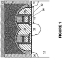
- Fig. 1 illustrates a pair of such memory cells formed on a semiconductor substrate 12.
- Source and drain diffusion regions 16/14 are formed in the substrate 12, defining a channel region 18 there between.
- Each of the memory cells has four conductive gates: a select gate 20 (also called a word line gate) disposed over and insulated from a first portion of the channel region 18, a floating gate 22 disposed over and insulated from a second portion of the channel region 18 and a portion of the source region 16, an erase gate 24 disposed over and insulated from the source region 16, and a control gate 26 disposed over and insulated from the floating gate 22.
- the erase gate 24 can have an upper portion that is disposed vertically over the floating gate 22 (e.g. a vertical overhang).
- the memory cells are arranged in an array, with columns of such memory cells separated by columns of isolation regions in an interlaced fashion.
- Each column of memory cells contains pairs of the memory cells in Fig. 1 arranged end to end, whereby each pair of memory cells share the same source region 16, and adjacent pairs share the same drain region 14.
- the select gates 20 for an entire row of the memory cells are formed as a single conductive line 20a (commonly referred to as a word line WL), such that each word line 20a forms the select gate 20 for one of the memory cells in each column of the memory cells (i.e. each word line electrically connects together a row of the select gates 20).
- the control gates 26 are similarly formed as a continuous control gate line 26a extending along the row of memory cells (i.e.
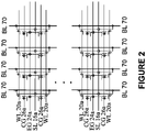
- Fig. 2 illustrates a schematic representation of a portion of the memory array.
- An individual target memory cell can be erased, programmed and read by applying various voltages to the selected lines for the target memory cell (i.e. the word line 20, bit line 70, source line 16, control gate line 26 and erase gate line 24 associated with the targeted memory cell), and by applying various voltages to the unselected lines (i.e. the word lines 20, bit lines 70, source lines 16, control gate lines 26 and erase gate lines 24 not associated with the targeted memory cell).
- the selected lines for the target memory cell i.e. the word line 20, bit line 70, source line 16, control gate line 26 and erase gate line 24 associated with the targeted memory cell.
- the following voltages may be applied to the selected (Sel.) lines and unselected (Unsel.) lines: WL (20) BL (70) SL (16) CG (26) EG (24) Sel. Unsel. Sel. Unsel. Sel. Unsel. Sel. Unsel. Sel. Unsel. Sel. Unsel. Unsel. Unsel. Unsel. 0nsel. 0v 0v or -6 to -9v 0v 9-11v or 7-9v 0v
- a voltage of 9-11 volts is applied to the erase gate 24, to cause electrons to tunnel from the floating gate 22 to the erase gate 24.
- An optional negative voltage on the order of -6 to -9 volts may be applied to the selected control gate 26. In that event, the voltage applied to the selected erase gate 24 may be lowered to approximately 7-9 volts. It is also known to use a voltage of 11.5 volts on the selected erase gate line 24, with zero voltages on all other lines.
- the following voltages may be applied to the selected (Sel.) lines and unselected (Unsel.) lines: WL (20) BL (70) SL (16) CG (26) EG (24) Sel. Unsel. Sel. Unsel. Sel. Unsel. Sel. Unsel. Sel. Unsel. 1-2v 0v 0.5-5uA 1.5-3v 3-6v 0v 6-9v 0v 6-9v 0v 0v 0v
- the target memory cell is programmed through efficient hot-electron injection with the portion of the channel under the floating gate in inversion.
- the medium voltage of 3-6 volts is applied to the selected source line SL to generate the hot electrons.
- the selected control gate 26 and erase gate 24 are biased to a high voltage (6-9 volts) to utilize the high coupling ratio and to maximize the voltage coupling to the floating gate 22.
- the high voltage coupled to the floating gate induces floating gate channel inversion and concentrates the lateral field in the split area to generate hot electrons more effectively, which are injected onto the floating gate 22.
- the voltages provide a high vertical field to attract hot electrons onto the floating gate and reduce the injection energy barrier.
- the following voltages may be applied to the selected (Sel.) lines and unselected (Unsel.) lines: WL (20) BL (70) SL (16) CG (26) EG (24) Sel. Unsel. Sel. Unsel. Sel. Unsel. Sel. Unsel. Sel. Unsel. Unsel. Unsel. Unsel. Unsel. 1.5-3.7v 0v 0.5-1.5v 0v 0v 0v 0v-3.7V 0v 0v-3.7V 0v 0v-3.7V 0v
- the voltages on the selected control gate 26 and the selected erase gate 24 can be balanced because each is coupled to the floating gate.
- the voltages applied to each of the selected control gates 26 and selected erase gates 24 can be a combination of voltages ranging from 0 to 3.7 volts to achieve an optimum window.
- voltages on the selected erase gate 24 can result in a faster read operation. It is also known in a read operation to apply a voltage of 1.2 volts on the selected word line and a voltage of 2.5 volts on the unselected control gate 26.
- the voltage on the select gate turns on (makes conductive) the portion of the channel region under the select gate 20. If the floating gate is programmed with electrons, the portion of the channel region under the floating gate will not conduct or provide little conduction. If the floating gate is not programmed with electrons, the channel region under the floating gate will be conductive. The conductivity of the channel region is sensed to determine if the floating gate is programmed with electrons or not.
- Generating a random number that is unique to the array of memory cells is accomplished by dedicating a predetermined number of the memory cells in the array for this purpose. These dedicated cells are preferably never programmed or erased, but instead are maintained in their original fabricated state (i.e. the program states of these memory cells are not changed from their program states that existed at the time the memory array is fabricated). It has been discovered that by reading these memory cells in pairs using differential sensing (which requires 4 memory cells for each bit of information), in subthreshold operation (meaning that the select gates are off so that the channel regions under the select gates are off, wherein any detected read current is leakage current only), that the leakage current provides a good measure of the randomness of the cells.
- Fig. 3 best illustrates this subthreshold, differential sensing.
- This figure schematically illustrates 8 memory cells (i.e., four pairs of memory cells), with each pair of memory cells extending in the column direction and connected to a different bit line 70, all sharing a common source line 16a.
- a subthreshold voltage e.g., 0.7V-1.5V
- I leakage current I for each of the pairs of memory cells on each of the bit lines, which is detected and measured by sense amplifiers 40.
- leakage current I 1 is generated from the first pair of cells on bit line 70 1 , where each of the memory cells leak current from its source to its drain and the total current leakage from the two memory cells is I 1 , I 2 is generated from the second pair of cells on bit line 70 2, I 3 is generated from the third pair of cells on bit line 70 3 , and so on.
- Differential sensing is accomplished by subtracting the total leakage current I 1 on bit line 70 1 from the total leakage current I 2 on bit line 70 2 to determine a first bit value (with a positive result being considered a 1 and a negative result being considered a 0), subtracting the total leakage current I 2 on bit line 70 2 from the total leakage current I 3 on bit line 70 3 to determine a second bit value (with a positive result being considered a 1 and a negative result being considered a 0), subtracting the total leakage current I 3 on bit line 70 3 from the total leakage current I 4 on bit line 70 4 to determine a third bit value (with a positive result being considered a 1 and a negative result being considered a 0), and so on.
- Each bit value of information is derived from the leakage current of four memory cells, combined onto two bit lines, with the two combined currents being subtracted from each other to yield a positive or negative result reflective of a single bit value. It is the combination of these single bit values for all of the dedicated memory cells that provides a number that is random (reflecting the randomness of the memory cell fabrication cell-to-cell). This combination of single bit values is unique to the memory cell array, and can be reliably and repeatably read from the memory cell array over the life of the product incorporating the memory cell array.
- Subtracting leakage currents can be implemented by actually subtracting one leakage current from another, or by subtracting leakage current values determined from the measured leakage currents. Differential sensing can instead be implemented by comparing measured leakage currents.
- Comparing leakage currents can be implemented by actually comparing two leakage currents, or by comparing leakage current values determined from the measured leakage currents. For example, the binary determination of 1 or 0 can be determined based on if the leakage current on the higher numbered bit line is greater than that on the lower numbered bit line.
- a dedicated pair of rows or even a sector of the memory cells for this random number generation. It may be desirable to utilize a buffer zone of memory cells (i.e. adjacent rows and/or columns) which are not used for any purpose. By not reading, programming or erasing cells in the buffer zone, the chances of disturbing the original randomness of the memory cells used for generating the random number are reduced.
- This technique has many advantages. First, by combining (summing) the current from two adjacent cells, the resulting current signal at any given bit line is roughly twice that of individual cells, making measurements more accurate. Second, because sensing/reading time is a function of current amplitude, the reading process is much faster. Third, differential sensing means that there need not be any threshold or reference value comparisons that can introduce error or drift over time. Fourth, random number generation is accomplished without structurally changing any of the memory array. Fifth, by grouping adjacent memory cells together and summing their current, fabrication similarities in adjacent cells are screened out.
- the memory cells used to generate the random number could be softly (i.e. lightly) programmed or erased. This could create artificial randomness that is greater than the natural randomness resulting just from fabrication variations.
- Other alternate embodiments include applying a small bias to the word lines 20a and/or control gate lines 26a so that the memory cells are closer to, but still under threshold, to increase the leakage current signals being measured by the sense amplifiers.
- more than one pair of memory cells on any given bit line can be used to generate leakage current to generate a higher total leakage current (i.e., two or more source lines 16a can be provided with the positive voltage to generate the leakage current through the memory cells connected thereto).
- the subthreshold voltage e.g., 0.7V-1.5V
- Fig. 4 illustrates an alternate embodiment of a split gate memory cell 30 with the same elements as the memory cell of Fig. 1 , but instead of having separate control and erase gates, there is a single program/erase (PE) gate 32 disposed over and insulated from the source region 16 (i.e. this is a three gate design).
- PE program/erase
- the memory cell pair can be erased by placing a high voltage on the PE gate 32 to induce tunneling of electrons from the floating gates 22 to the PE gate 32.
- each memory cell can be programmed by placing positive voltages on the select gate 20, PE gate 32 and source region 16, and a current on drain region 14, to inject electrons from the current flowing through the channel region 18 onto floating gate 22.
- Each memory cell can be read by placing positive voltages on the select gate 20 and drain region 14, and sensing current flow.
- Fig. 5 illustrates another alternate embodiment of a split gate memory cell with the same elements as the memory cell of Fig. 1 , but without any control or erase gates.
- the select gate 20 has an upper portion that extends up and over the floating gate 22.
- the memory cell can be erased by placing a high positive voltage on the select gate 20, and a reference potential on the source and drain regions 16/14, to induce tunneling of electrons from the floating gate 22 to the select gate 20.
- the memory cell can be programmed by applying a ground potential to drain region 14, a positive voltage on source region 16, and a positive voltage on the select gate 20.
- Electrons will then flow from the drain region 14 toward the source region 16, with some electrons becoming accelerated and heated whereby they are injected onto the floating gate 22 (leaving the floating gate negatively charged - the programmed state).
- the memory cell can be read by placing ground potential on the drain region 14, a positive voltage on the source region 16 and a positive voltage on the control gate 22 (turning on the channel region portion under the control gate 22), and sensing current flow.
- the architecture of the memory device of the present invention is illustrated in Fig. 6 .
- the memory device includes an array 50 of non-volatile memory cells, which can be segregated into two separate planes (Plane A 52a and Plane B 52b).
- the memory cells can be of the type shown in Figures 1 and 4-5 , formed on a single chip, arranged in a plurality of rows and columns in the semiconductor substrate 12. Adjacent to the array of non-volatile memory cells are address decoders (e.g.
- XDEC 54 (row decoder), SLDRV 56, YMUX 58 (column decoder), HVDEC 60) and a bit line controller (BLINHCTL 62), which are used to decode addresses and supply the various voltages to the various memory cell gates and regions during read, program, and erase operations for selected memory cells.
- the column decoder includes the sense amplifiers 40.
- Controller 66 (containing control circuitry) controls the various device elements to implement each operation (program, erase, read) on target memory cells.
- Charge pump CHRGPMP 64 provides the various voltages used to read, program and erase the memory cells under the control of the controller 66. Controller 66 also implements the above described differential sensing in subthreshold operation to determine the random number associated with the memory device.
- the term “adjacent” includes “directly adjacent” (no intermediate materials, elements or space disposed there between) and “indirectly adjacent” (intermediate materials, elements or space disposed there between), “mounted to” includes “directly mounted to” (no intermediate materials, elements or space disposed there between) and “indirectly mounted to” (intermediate materials, elements or spaced disposed there between), and “electrically coupled” includes “directly electrically coupled to” (no intermediate materials or elements there between that electrically connect the elements together) and “indirectly electrically coupled to” (intermediate materials or elements there between that electrically connect the elements together).
- forming an element "over a substrate” can include forming the element directly on the substrate with no intermediate materials/elements there between, as well as forming the element indirectly on the substrate with one or more intermediate materials/elements there between.
Landscapes
- Engineering & Computer Science (AREA)
- Microelectronics & Electronic Packaging (AREA)
- Theoretical Computer Science (AREA)
- Physics & Mathematics (AREA)
- General Physics & Mathematics (AREA)
- Computer Security & Cryptography (AREA)
- General Engineering & Computer Science (AREA)
- Computer Hardware Design (AREA)
- Computational Mathematics (AREA)
- Pure & Applied Mathematics (AREA)
- Mathematical Optimization (AREA)
- Mathematical Analysis (AREA)
- Software Systems (AREA)
- Mathematical Physics (AREA)
- Computer Networks & Wireless Communication (AREA)
- Signal Processing (AREA)
- Non-Volatile Memory (AREA)
- Read Only Memory (AREA)
- Semiconductor Memories (AREA)
Claims (16)
- Speichervorrichtung, umfassend:eine Vielzahl von Speicherzellen, wobei jede der Speicherzellen einschließt:eine erste und eine zweite Region, die in einem Halbleitersubstrat (12) ausgebildet sind, wobei sich eine Kanalregion (18) des Substrats (12) zwischen der ersten und der zweiten Region erstreckt,ein Floating-Gate (22), das über einem ersten Abschnitt der Kanalregion (18) angeordnet und von diesem isoliert ist, undein Auswahl-Gate (20), das über einem zweiten Abschnitt der Kanalregion (18) angeordnet und von diesem isoliert ist;eine Steuerung (66), die konfiguriert ist zum:Anlegen einer oder mehrerer positiver Spannungen an die ersten Regionen der Speicherzellen, während sich die Speicherzellen in einem unterschwelligen Zustand befinden, um Leckstrom durch jede der Kanalregionen (18) zu erzeugen,Messen der Leckströme undErzeugen einer Zufallszahl auf Basis der gemessenen Leckströme;wobei die Steuerung (66) dazu konfiguriert ist, mindestens einen Teil der Zufallszahl zu erzeugen, indem die gemessenen Leckströme für ein erstes Paar der Speicherzellen von den gemessenen Leckströmen für ein zweites Paar der Speicherzellen subtrahiert bzw. mit diesen verglichen werden.
- Speichervorrichtung nach Anspruch 1, wobei jede der Speicherzellen ferner umfasst:ein Lösch-Gate (24), das über der ersten Region angeordnet und von dieser isoliert ist; undwobei jede der Speicherzellen ferner umfasst:
ein Steuer-Gate (26), das über dem Floating-Gate (22) angeordnet und von diesem isoliert ist. - Speichervorrichtung nach Anspruch 1, wobei die Steuerung ferner konfiguriert ist zum:
Anlegen einer positiven Spannung an die Auswahl-Gates (20), während sich die Speicherzellen in einem unterschwelligen Zustand befinden. - Speichervorrichtung nach Anspruch 2, wobei die Steuerung ferner konfiguriert ist zum:
Anlegen einer positiven Spannung an die Steuer-Gates (26), während sich die Speicherzellen in einem unterschwelligen Zustand befinden. - Speichervorrichtung nach Anspruch 1, wobei:das erste Paar der Speicherzellen aneinander angrenzend angeordnet ist und das zweite Paar der Speicherzellen aneinander angrenzend angeordnet ist;die Vorrichtung ferner umfasst:eine erste Bit-Leitung, die mit den zweiten Regionen des ersten Paares von Speicherzellen verbunden ist;eine zweite Bit-Leitung, die mit den zweiten Regionen des zweiten Paares von Speicherzellen verbunden ist;das Erzeugen der Zufallszahl mindestens teilweise das Subtrahieren oder Vergleichen von Leckströmen auf der ersten Bit-Leitung von bzw. mit Leckströmen auf der zweiten Bit-Leitung einschließt.
- Speichervorrichtung nach Anspruch 1, wobei:das erste Paar der Speicherzellen aneinander angrenzend angeordnet ist und das zweite Paar der Speicherzellen aneinander angrenzend angeordnet ist;die Vorrichtung ferner umfasst:eine erste Bit-Leitung, die mit den ersten Regionen des ersten Paares von Speicherzellen verbunden ist;eine zweite Bit-Leitung, die mit den ersten Regionen des zweiten Paares von Speicherzellen verbunden ist;das Erzeugen der Zufallszahl mindestens teilweise das Subtrahieren oder Vergleichen von Leckströmen auf der ersten Bit-Leitung von bzw. mit Leckströmen auf der zweiten Bit-Leitung einschließt.
- Speichervorrichtung, umfassend:eine Vielzahl von Paaren von Speicherzellen, wobei jedes Paar der Speicherzellen einschließt:eine erste, eine zweite und eine dritte Region, die in einem Halbleitersubstrat (12) ausgebildet sind, wobei sich eine erste Kanalregion (18) des Substrats (12) zwischen der ersten und der zweiten Region erstreckt und sich eine zweite Kanalregion (18) des Substrats (12) zwischen der zweiten und der dritten Region erstreckt,ein erstes Floating-Gate, das über einem ersten Abschnitt der ersten Kanalregion angeordnet und von diesem isoliert ist,ein zweites Floating-Gate, das über einem ersten Abschnitt der zweiten Kanalregion angeordnet und von diesem isoliert ist,ein erstes Auswahl-Gate, das über einem zweiten Abschnitt der ersten Kanalregion angeordnet und von diesem isoliert ist, undein zweites Auswahl-Gate, das über einem zweiten Abschnitt der zweiten Kanalregion angeordnet und von diesem isoliert ist;eine Steuerung (66), die konfiguriert ist zum:Anlegen einer oder mehrerer positiver Spannungen an die zweiten Regionen oder an die erste und die dritte Region der Speicherzellen, während sich die Speicherzellen in einem unterschwelligen Zustand befinden, um Leckstrom durch jede der ersten und der zweiten Kanalregion zu erzeugen,Messen der Leckströme undErzeugen einer Zufallszahl auf Basis der gemessenen Leckströme;wobei die Steuerung dazu konfiguriert ist, mindestens einen Teil der Zufallszahl zu erzeugen, indem die gemessenen Leckströme für das erste Paar der Speicherzellen von den gemessenen Leckströmen für das zweite Paar der Speicherzellen subtrahiert bzw. mit diesen verglichen werden.
- Speichervorrichtung nach Anspruch 7, wobei:die Vorrichtung ferner eine Vielzahl von Bit-Leitungen (70) umfasst, die jeweils mit der ersten und der dritten Region für eines der Paare von Speicherzellen verbunden ist, um die Leckströme von der ersten und der zweiten Kanalregion für das eine Paar der Speicherzellen zu empfangen;das Erzeugen der Zufallszahl mindestens teilweise das Subtrahieren oder Vergleichen von Leckströmen auf einer der Bit-Leitungen (70) von bzw. mit Leckströmen auf einer anderen der Bit-Leitungen (70) einschließt; undwobei für jede der Bit-Leitungen (70) die Leckströme darauf der Leckstrom von der ersten Kanalregion und der Leckstrom von der zweiten Kanalregion für das eine Paar von Speicherzellen sind.
- Verfahren zum Identifizieren einer Speichervorrichtung, die eine Vielzahl von Speicherzellen einschließt, wobei jede der Speicherzellen einschließt:eine erste und eine zweite Region, die in einem Halbleitersubstrat (12) ausgebildet sind, wobei sich eine Kanalregion (18) des Substrats (12) zwischen der ersten und der zweiten Region erstreckt,ein Floating-Gate (22), das über einem ersten Abschnitt der Kanalregion (18) angeordnet und von diesem isoliert ist, undein Auswahl-Gate (20), das über einem zweiten Abschnitt der Kanalregion (18) angeordnet und von diesem isoliert ist;das Verfahren umfassend:Anlegen einer oder mehrerer positiver Spannungen an die ersten Regionen der Speicherzellen, während sich die Speicherzellen in einem unterschwelligen Zustand befinden, um Leckstrom durch jede der Kanalregionen (18) zu erzeugen,Messen der Leckströme undErzeugen einer Zufallszahl auf Basis der gemessenen Leckströme;wobei das Erzeugen der Zufallszahl mindestens teilweise das Subtrahieren oder Vergleichen der gemessenen Leckströme für ein erstes Paar der Speicherzellen von bzw. mit den gemessenen Leckströmen für ein zweites Paar der Speicherzellen einschließt.
- Verfahren nach Anspruch 9, wobei:das erste Paar der Speicherzellen aneinander angrenzend angeordnet ist und das zweite Paar der Speicherzellen aneinander angrenzend angeordnet ist;die Vorrichtung ferner umfasst:eine erste Bit-Leitung, die mit den zweiten Regionen des ersten Paares von Speicherzellen verbunden ist;eine zweite Bit-Leitung, die mit den zweiten Regionen des zweiten Paares von Speicherzellen verbunden ist;das Erzeugen der Zufallszahl mindestens teilweise das Subtrahieren oder Vergleichen von Leckströmen auf der ersten Bit-Leitung von bzw. mit Leckströmen auf der zweiten Bit-Leitung einschließt.
- Verfahren nach Anspruch 9, wobei:das erste Paar der Speicherzellen aneinander angrenzend angeordnet ist und das zweite Paar der Speicherzellen aneinander angrenzend angeordnet ist;die Vorrichtung ferner umfasst:eine erste Bit-Leitung, die mit den ersten Regionen des ersten Paares von Speicherzellen verbunden ist;eine zweite Bit-Leitung, die mit den ersten Regionen des zweiten Paares von Speicherzellen verbunden ist;das Erzeugen der Zufallszahl mindestens teilweise das Subtrahieren oder Vergleichen von Leckströmen auf der ersten Bit-Leitung von bzw. mit Leckströmen auf der zweiten Bit-Leitung einschließt.
- Verfahren nach Anspruch 9, wobei jede der Speicherzellen ferner umfasst:ein Lösch-Gate (24), das über der ersten Region angeordnet und von dieser isoliert ist; undwobei jede der Speicherzellen ferner umfasst:
ein Steuer-Gate (26), das über dem Floating-Gate (22) angeordnet und von diesem isoliert ist. - Verfahren nach Anspruch 9, ferner umfassend:
Anlegen einer positiven Spannung an die Auswahl-Gates (20), während sich die Speicherzellen in einem unterschwelligen Zustand befinden. - Verfahren nach Anspruch 12, ferner umfassend:
Anlegen einer positiven Spannung an die Steuer-Gates (26), während sich die Speicherzellen in einem unterschwelligen Zustand befinden. - Verfahren zum Identifizieren einer Speichervorrichtung, die eine Vielzahl von Paaren von Speicherzellen einschließt, wobei jedes Paar der Speicherzellen einschließt:eine erste, eine zweite und eine dritte Region, die in einem Halbleitersubstrat (12) ausgebildet sind, wobei sich eine erste Kanalregion (18) des Substrats (12) zwischen der ersten und der zweiten Region erstreckt und sich eine zweite Kanalregion (18) des Substrats (12) zwischen der zweiten und der dritten Region erstreckt,ein erstes Floating-Gate, das über einem ersten Abschnitt der ersten Kanalregion angeordnet und von diesem isoliert ist,ein zweites Floating-Gate, das über einem ersten Abschnitt der zweiten Kanalregion angeordnet und von diesem isoliert ist,ein erstes Auswahl-Gate, das über einem zweiten Abschnitt der ersten Kanalregion angeordnet und von diesem isoliert ist, undein zweites Auswahl-Gate, das über einem zweiten Abschnitt der zweiten Kanalregion angeordnet und von diesem isoliert ist;das Verfahren umfassend:Anlegen einer oder mehrerer positiver Spannungen an die zweiten Regionen oder an die erste und die dritte Region der Speicherzellen, während sich die Speicherzellen in einem unterschwelligen Zustand befinden, um Leckstrom durch jede der ersten und der zweiten Kanalregion zu erzeugen,Messen der Leckströme undErzeugen einer Zufallszahl auf Basis der gemessenen Leckströme und/oderwobei das Erzeugen der Zufallszahl mindestens teilweise das Subtrahieren oder Vergleichen der gemessenen Leckströme für das erste Paar der Speicherzellen von bzw. mit den gemessenen Leckströmen für das zweite Paar der Speicherzellen einschließt.
- Verfahren nach Anspruch 15, wobei:die Vorrichtung ferner eine Vielzahl von Bit-Leitungen (70) umfasst, die jeweils mit der ersten und der dritten Region für eines der Paare von Speicherzellen verbunden ist, um die Leckströme von der ersten und der zweiten Kanalregion für das eine Paar der Speicherzellen zu empfangen;das Erzeugen der Zufallszahl mindestens teilweise das Subtrahieren oder Vergleichen von Leckströmen auf einer der Bit-Leitungen (70) von bzw. mit Leckströmen auf einer anderen der Bit-Leitungen (70) einschließt; undwobei für jede der Bit-Leitungen (70) die Leckströme darauf der Leckstrom von der ersten Kanalregion und der Leckstrom von der zweiten Kanalregion für das eine Paar von Speicherzellen sind.
Applications Claiming Priority (3)
| Application Number | Priority Date | Filing Date | Title |
|---|---|---|---|
| US201762479193P | 2017-03-30 | 2017-03-30 | |
| US15/905,720 US10381088B2 (en) | 2017-03-30 | 2018-02-26 | System and method for generating random numbers based on non-volatile memory cell array entropy |
| PCT/US2018/020628 WO2018182922A1 (en) | 2017-03-30 | 2018-03-02 | System and method for generating random numbers based on non-volatile memory cell array entropy |
Publications (3)
| Publication Number | Publication Date |
|---|---|
| EP3602084A1 EP3602084A1 (de) | 2020-02-05 |
| EP3602084A4 EP3602084A4 (de) | 2020-07-15 |
| EP3602084B1 true EP3602084B1 (de) | 2022-05-04 |
Family
ID=63669848
Family Applications (1)
| Application Number | Title | Priority Date | Filing Date |
|---|---|---|---|
| EP18777218.1A Active EP3602084B1 (de) | 2017-03-30 | 2018-03-02 | System und verfahren zur erzeugung von zufallszahlen auf basis der zellenanordnungsentropie eines nichtflüchtigen speichers |
Country Status (7)
| Country | Link |
|---|---|
| US (1) | US10381088B2 (de) |
| EP (1) | EP3602084B1 (de) |
| JP (1) | JP6783397B2 (de) |
| KR (1) | KR102208056B1 (de) |
| CN (1) | CN110462582B (de) |
| TW (1) | TWI683110B (de) |
| WO (1) | WO2018182922A1 (de) |
Families Citing this family (4)
| Publication number | Priority date | Publication date | Assignee | Title |
|---|---|---|---|---|
| US10970046B2 (en) | 2019-02-22 | 2021-04-06 | International Business Machines Corporation | Random number generator compatible with complementary metal-oxide semiconductor technology |
| GB2583118B (en) * | 2019-04-17 | 2021-09-08 | Crypto Quantique Ltd | Device identification with quantum tunnelling currents |
| CN112306455B (zh) * | 2020-03-26 | 2024-02-06 | 神州融安数字科技(北京)有限公司 | 随机数生成方法、生成器、电子设备计算机可读存储介质 |
| CN117529776A (zh) * | 2021-03-21 | 2024-02-06 | Gsi 科技公司 | Ram真随机数生成器 |
Family Cites Families (21)
| Publication number | Priority date | Publication date | Assignee | Title |
|---|---|---|---|---|
| US5455792A (en) * | 1994-09-09 | 1995-10-03 | Yi; Yong-Wan | Flash EEPROM devices employing mid channel injection |
| US6161213A (en) * | 1999-02-17 | 2000-12-12 | Icid, Llc | System for providing an integrated circuit with a unique identification |
| US6222227B1 (en) | 1999-08-09 | 2001-04-24 | Actrans System Inc. | Memory cell with self-aligned floating gate and separate select gate, and fabrication process |
| JP4044755B2 (ja) * | 2000-12-12 | 2008-02-06 | 三星電子株式会社 | 不揮発性半導体メモリ装置及びそれのプログラム方法 |
| JP3959264B2 (ja) * | 2001-09-29 | 2007-08-15 | 株式会社東芝 | 積層型半導体装置 |
| US7142452B1 (en) | 2004-06-07 | 2006-11-28 | Virage Logic Corporation | Method and system for securing data in a multi-time programmable non-volatile memory device |
| US7050344B1 (en) * | 2004-11-04 | 2006-05-23 | Promos Technologies Inc. | Failure test method for split gate flash memory |
| JP4927164B2 (ja) * | 2007-04-12 | 2012-05-09 | ルネサスエレクトロニクス株式会社 | 半導体装置 |
| US20090039410A1 (en) | 2007-08-06 | 2009-02-12 | Xian Liu | Split Gate Non-Volatile Flash Memory Cell Having A Floating Gate, Control Gate, Select Gate And An Erase Gate With An Overhang Over The Floating Gate, Array And Method Of Manufacturing |
| US7894294B2 (en) * | 2008-01-23 | 2011-02-22 | Mosaid Technologies Incorporated | Operational mode control in serial-connected memory based on identifier |
| US8417754B2 (en) | 2009-05-11 | 2013-04-09 | Empire Technology Development, Llc | Identification of integrated circuits |
| US9105432B2 (en) * | 2011-03-31 | 2015-08-11 | Ictk Co., Ltd | Apparatus and method for generating digital value |
| CN103247625A (zh) * | 2012-02-03 | 2013-08-14 | 华邦电子股份有限公司 | 非易失性存储器元件及其阵列 |
| US8867271B2 (en) * | 2012-05-30 | 2014-10-21 | Sandisk Technologies Inc. | Threshold voltage adjustment for a select gate transistor in a stacked non-volatile memory device |
| US9323499B2 (en) | 2012-11-15 | 2016-04-26 | Elwha Llc | Random number generator functions in memory |
| US9275748B2 (en) * | 2013-03-14 | 2016-03-01 | Silicon Storage Technology, Inc. | Low leakage, low threshold voltage, split-gate flash cell operation |
| CN105027216B (zh) * | 2013-03-14 | 2017-09-22 | 硅存储技术公司 | 非易失性存储器编程算法装置和方法 |
| WO2014182672A1 (en) * | 2013-05-07 | 2014-11-13 | Wilber Scott A | Acquisition and assessment of classically non-inferable information |
| KR20160050534A (ko) * | 2014-10-30 | 2016-05-11 | 에스케이하이닉스 주식회사 | 누설 전류 감지부를 구비하는 반도체 집적 회로 장치 및 그 구동방법 |
| US9548113B2 (en) * | 2014-11-21 | 2017-01-17 | Panasonic Intellectual Property Management Co., Ltd. | Tamper-resistant non-volatile memory device |
| JP6587188B2 (ja) * | 2015-06-18 | 2019-10-09 | パナソニックIpマネジメント株式会社 | 乱数処理装置、集積回路カード、および乱数処理方法 |
-
2018
- 2018-02-26 US US15/905,720 patent/US10381088B2/en active Active
- 2018-03-02 KR KR1020197032175A patent/KR102208056B1/ko active Active
- 2018-03-02 CN CN201880019158.XA patent/CN110462582B/zh active Active
- 2018-03-02 EP EP18777218.1A patent/EP3602084B1/de active Active
- 2018-03-02 JP JP2019553226A patent/JP6783397B2/ja active Active
- 2018-03-02 WO PCT/US2018/020628 patent/WO2018182922A1/en not_active Ceased
- 2018-03-20 TW TW107109424A patent/TWI683110B/zh active
Also Published As
| Publication number | Publication date |
|---|---|
| US10381088B2 (en) | 2019-08-13 |
| CN110462582B (zh) | 2020-10-23 |
| US20180286486A1 (en) | 2018-10-04 |
| JP2020516071A (ja) | 2020-05-28 |
| TW201903419A (zh) | 2019-01-16 |
| JP6783397B2 (ja) | 2020-11-11 |
| CN110462582A (zh) | 2019-11-15 |
| KR102208056B1 (ko) | 2021-01-27 |
| EP3602084A1 (de) | 2020-02-05 |
| KR20190133236A (ko) | 2019-12-02 |
| TWI683110B (zh) | 2020-01-21 |
| WO2018182922A1 (en) | 2018-10-04 |
| EP3602084A4 (de) | 2020-07-15 |
Similar Documents
| Publication | Publication Date | Title |
|---|---|---|
| US10460811B2 (en) | Array of three-gate flash memory cells with individual memory cell read, program and erase | |
| US10388389B2 (en) | Flash memory array with individual memory cell read, program and erase | |
| JP6937747B2 (ja) | 完全空乏型シリコン・オン・インシュレータ・フラッシュメモリ設計 | |
| EP2973581B1 (de) | Split-gate-flashzellenbetrieb mit niedrigem leckstrom und niedriger schwellenspannung | |
| US6829171B2 (en) | Memory device trapping charges in insulating film to store information in non-volatile manner | |
| US9613709B2 (en) | Dual non-volatile memory cell comprising an erase transistor | |
| US10134475B2 (en) | Method and apparatus for inhibiting the programming of unselected bitlines in a flash memory system | |
| CN204991153U (zh) | 存储器单元和非易失性存储器 | |
| US20150213898A1 (en) | Byte Erasable Non-volatile Memory Architecture And Method Of Erasing Same | |
| EP3602084B1 (de) | System und verfahren zur erzeugung von zufallszahlen auf basis der zellenanordnungsentropie eines nichtflüchtigen speichers | |
| KR100491912B1 (ko) | 불휘발성 반도체 메모리 | |
| US10790021B2 (en) | EEPROM, and methods for erasing, programming and reading the EEPROM | |
| US20080130367A1 (en) | Byte-Erasable Nonvolatile Memory Devices | |
| TW201931376A (zh) | 用於在非揮發性記憶體中使用電流乘數儲存並檢索多位元資料的系統及方法 | |
| US12148473B2 (en) | Non-volatile memory cell with single poly, floating gate extending over two wells | |
| US20070091682A1 (en) | Byte-Erasable Nonvolatile Memory Devices | |
| TW201541455A (zh) | 電性可程式化唯讀記憶體單元陣列、操作其之方法以及包含其之記憶體裝置 | |
| US20250208774A1 (en) | Programmable logic block comprising flash memory array to store configuration data for programmable logic | |
| US20260112419A1 (en) | Tracking memory cells for current leakage compensation in non-volatile memory array |
Legal Events
| Date | Code | Title | Description |
|---|---|---|---|
| STAA | Information on the status of an ep patent application or granted ep patent |
Free format text: STATUS: THE INTERNATIONAL PUBLICATION HAS BEEN MADE |
|
| PUAI | Public reference made under article 153(3) epc to a published international application that has entered the european phase |
Free format text: ORIGINAL CODE: 0009012 |
|
| STAA | Information on the status of an ep patent application or granted ep patent |
Free format text: STATUS: REQUEST FOR EXAMINATION WAS MADE |
|
| 17P | Request for examination filed |
Effective date: 20191030 |
|
| AK | Designated contracting states |
Kind code of ref document: A1 Designated state(s): AL AT BE BG CH CY CZ DE DK EE ES FI FR GB GR HR HU IE IS IT LI LT LU LV MC MK MT NL NO PL PT RO RS SE SI SK SM TR |
|
| AX | Request for extension of the european patent |
Extension state: BA ME |
|
| DAV | Request for validation of the european patent (deleted) | ||
| DAX | Request for extension of the european patent (deleted) | ||
| A4 | Supplementary search report drawn up and despatched |
Effective date: 20200615 |
|
| RIC1 | Information provided on ipc code assigned before grant |
Ipc: G11C 16/24 20060101ALI20200608BHEP Ipc: G11C 16/28 20060101ALI20200608BHEP Ipc: G06F 7/58 20060101ALI20200608BHEP Ipc: H04L 9/32 20060101ALN20200608BHEP Ipc: H01L 29/423 20060101ALI20200608BHEP Ipc: G06F 21/79 20130101ALI20200608BHEP Ipc: G11C 29/50 20060101AFI20200608BHEP Ipc: H01L 27/11521 20170101ALI20200608BHEP Ipc: G11C 16/04 20060101ALI20200608BHEP Ipc: G06F 21/73 20130101ALI20200608BHEP Ipc: G11C 16/22 20060101ALI20200608BHEP Ipc: G11C 29/44 20060101ALN20200608BHEP |
|
| RIC1 | Information provided on ipc code assigned before grant |
Ipc: H04L 9/08 20060101ALI20210218BHEP Ipc: G11C 29/44 20060101ALN20210218BHEP Ipc: G11C 16/04 20060101ALI20210218BHEP Ipc: G11C 16/28 20060101ALI20210218BHEP Ipc: G11C 16/24 20060101ALI20210218BHEP Ipc: G11C 29/50 20060101AFI20210218BHEP Ipc: G06F 21/79 20130101ALI20210218BHEP Ipc: H01L 29/423 20060101ALI20210218BHEP Ipc: H04L 9/32 20060101ALN20210218BHEP Ipc: G06F 21/73 20130101ALI20210218BHEP Ipc: G09C 1/00 20060101ALI20210218BHEP Ipc: H01L 27/11521 20170101ALI20210218BHEP Ipc: G06F 7/58 20060101ALI20210218BHEP Ipc: G11C 16/22 20060101ALI20210218BHEP |
|
| RIC1 | Information provided on ipc code assigned before grant |
Ipc: G11C 16/22 20060101ALI20210303BHEP Ipc: H01L 29/423 20060101ALI20210303BHEP Ipc: H04L 9/32 20060101ALN20210303BHEP Ipc: G11C 16/24 20060101ALI20210303BHEP Ipc: G11C 29/44 20060101ALN20210303BHEP Ipc: G11C 16/04 20060101ALI20210303BHEP Ipc: H04L 9/08 20060101ALI20210303BHEP Ipc: G06F 21/79 20130101ALI20210303BHEP Ipc: G11C 29/50 20060101AFI20210303BHEP Ipc: G11C 16/28 20060101ALI20210303BHEP Ipc: G09C 1/00 20060101ALI20210303BHEP Ipc: G06F 7/58 20060101ALI20210303BHEP Ipc: G06F 21/73 20130101ALI20210303BHEP Ipc: H01L 27/11521 20170101ALI20210303BHEP |
|
| RIC1 | Information provided on ipc code assigned before grant |
Ipc: H04L 9/32 20060101ALN20210401BHEP Ipc: G11C 29/44 20060101ALN20210401BHEP Ipc: H04L 9/08 20060101ALI20210401BHEP Ipc: H01L 29/423 20060101ALI20210401BHEP Ipc: H01L 27/11521 20170101ALI20210401BHEP Ipc: G09C 1/00 20060101ALI20210401BHEP Ipc: G06F 7/58 20060101ALI20210401BHEP Ipc: G06F 21/79 20130101ALI20210401BHEP Ipc: G06F 21/73 20130101ALI20210401BHEP Ipc: G11C 16/28 20060101ALI20210401BHEP Ipc: G11C 16/24 20060101ALI20210401BHEP Ipc: G11C 16/22 20060101ALI20210401BHEP Ipc: G11C 16/04 20060101ALI20210401BHEP Ipc: G11C 29/50 20060101AFI20210401BHEP |
|
| GRAP | Despatch of communication of intention to grant a patent |
Free format text: ORIGINAL CODE: EPIDOSNIGR1 |
|
| STAA | Information on the status of an ep patent application or granted ep patent |
Free format text: STATUS: GRANT OF PATENT IS INTENDED |
|
| RIC1 | Information provided on ipc code assigned before grant |
Ipc: H04L 9/32 20060101ALN20210503BHEP Ipc: G11C 29/44 20060101ALN20210503BHEP Ipc: H04L 9/08 20060101ALI20210503BHEP Ipc: H01L 29/423 20060101ALI20210503BHEP Ipc: H01L 27/11521 20170101ALI20210503BHEP Ipc: G09C 1/00 20060101ALI20210503BHEP Ipc: G06F 7/58 20060101ALI20210503BHEP Ipc: G06F 21/79 20130101ALI20210503BHEP Ipc: G06F 21/73 20130101ALI20210503BHEP Ipc: G11C 16/28 20060101ALI20210503BHEP Ipc: G11C 16/24 20060101ALI20210503BHEP Ipc: G11C 16/22 20060101ALI20210503BHEP Ipc: G11C 16/04 20060101ALI20210503BHEP Ipc: G11C 29/50 20060101AFI20210503BHEP |
|
| INTG | Intention to grant announced |
Effective date: 20210521 |
|
| GRAJ | Information related to disapproval of communication of intention to grant by the applicant or resumption of examination proceedings by the epo deleted |
Free format text: ORIGINAL CODE: EPIDOSDIGR1 |
|
| STAA | Information on the status of an ep patent application or granted ep patent |
Free format text: STATUS: REQUEST FOR EXAMINATION WAS MADE |
|
| REG | Reference to a national code |
Ref country code: DE Ref legal event code: R079 Ref document number: 602018035033 Country of ref document: DE Free format text: PREVIOUS MAIN CLASS: G01R0019000000 Ipc: G11C0029500000 |
|
| INTC | Intention to grant announced (deleted) | ||
| RIC1 | Information provided on ipc code assigned before grant |
Ipc: H04L 9/32 20060101ALN20210922BHEP Ipc: G11C 29/44 20060101ALN20210922BHEP Ipc: H04L 9/08 20060101ALI20210922BHEP Ipc: H01L 29/423 20060101ALI20210922BHEP Ipc: H01L 27/11521 20170101ALI20210922BHEP Ipc: G09C 1/00 20060101ALI20210922BHEP Ipc: G06F 7/58 20060101ALI20210922BHEP Ipc: G06F 21/79 20130101ALI20210922BHEP Ipc: G06F 21/73 20130101ALI20210922BHEP Ipc: G11C 16/28 20060101ALI20210922BHEP Ipc: G11C 16/24 20060101ALI20210922BHEP Ipc: G11C 16/22 20060101ALI20210922BHEP Ipc: G11C 16/04 20060101ALI20210922BHEP Ipc: G11C 29/50 20060101AFI20210922BHEP |
|
| RIC1 | Information provided on ipc code assigned before grant |
Ipc: H04L 9/32 20060101ALN20211020BHEP Ipc: G11C 29/44 20060101ALN20211020BHEP Ipc: H04L 9/08 20060101ALI20211020BHEP Ipc: H01L 29/423 20060101ALI20211020BHEP Ipc: H01L 27/11521 20170101ALI20211020BHEP Ipc: G09C 1/00 20060101ALI20211020BHEP Ipc: G06F 7/58 20060101ALI20211020BHEP Ipc: G06F 21/79 20130101ALI20211020BHEP Ipc: G06F 21/73 20130101ALI20211020BHEP Ipc: G11C 16/28 20060101ALI20211020BHEP Ipc: G11C 16/24 20060101ALI20211020BHEP Ipc: G11C 16/22 20060101ALI20211020BHEP Ipc: G11C 16/04 20060101ALI20211020BHEP Ipc: G11C 29/50 20060101AFI20211020BHEP |
|
| GRAP | Despatch of communication of intention to grant a patent |
Free format text: ORIGINAL CODE: EPIDOSNIGR1 |
|
| STAA | Information on the status of an ep patent application or granted ep patent |
Free format text: STATUS: GRANT OF PATENT IS INTENDED |
|
| INTG | Intention to grant announced |
Effective date: 20211126 |
|
| GRAS | Grant fee paid |
Free format text: ORIGINAL CODE: EPIDOSNIGR3 |
|
| GRAA | (expected) grant |
Free format text: ORIGINAL CODE: 0009210 |
|
| STAA | Information on the status of an ep patent application or granted ep patent |
Free format text: STATUS: THE PATENT HAS BEEN GRANTED |
|
| AK | Designated contracting states |
Kind code of ref document: B1 Designated state(s): AL AT BE BG CH CY CZ DE DK EE ES FI FR GB GR HR HU IE IS IT LI LT LU LV MC MK MT NL NO PL PT RO RS SE SI SK SM TR |
|
| REG | Reference to a national code |
Ref country code: GB Ref legal event code: FG4D |
|
| REG | Reference to a national code |
Ref country code: CH Ref legal event code: EP |
|
| REG | Reference to a national code |
Ref country code: AT Ref legal event code: REF Ref document number: 1489983 Country of ref document: AT Kind code of ref document: T Effective date: 20220515 |
|
| REG | Reference to a national code |
Ref country code: IE Ref legal event code: FG4D Ref country code: DE Ref legal event code: R096 Ref document number: 602018035033 Country of ref document: DE |
|
| REG | Reference to a national code |
Ref country code: NL Ref legal event code: FP |
|
| REG | Reference to a national code |
Ref country code: LT Ref legal event code: MG9D |
|
| REG | Reference to a national code |
Ref country code: AT Ref legal event code: MK05 Ref document number: 1489983 Country of ref document: AT Kind code of ref document: T Effective date: 20220504 |
|
| PG25 | Lapsed in a contracting state [announced via postgrant information from national office to epo] |
Ref country code: SE Free format text: LAPSE BECAUSE OF FAILURE TO SUBMIT A TRANSLATION OF THE DESCRIPTION OR TO PAY THE FEE WITHIN THE PRESCRIBED TIME-LIMIT Effective date: 20220504 Ref country code: PT Free format text: LAPSE BECAUSE OF FAILURE TO SUBMIT A TRANSLATION OF THE DESCRIPTION OR TO PAY THE FEE WITHIN THE PRESCRIBED TIME-LIMIT Effective date: 20220905 Ref country code: NO Free format text: LAPSE BECAUSE OF FAILURE TO SUBMIT A TRANSLATION OF THE DESCRIPTION OR TO PAY THE FEE WITHIN THE PRESCRIBED TIME-LIMIT Effective date: 20220804 Ref country code: LT Free format text: LAPSE BECAUSE OF FAILURE TO SUBMIT A TRANSLATION OF THE DESCRIPTION OR TO PAY THE FEE WITHIN THE PRESCRIBED TIME-LIMIT Effective date: 20220504 Ref country code: HR Free format text: LAPSE BECAUSE OF FAILURE TO SUBMIT A TRANSLATION OF THE DESCRIPTION OR TO PAY THE FEE WITHIN THE PRESCRIBED TIME-LIMIT Effective date: 20220504 Ref country code: GR Free format text: LAPSE BECAUSE OF FAILURE TO SUBMIT A TRANSLATION OF THE DESCRIPTION OR TO PAY THE FEE WITHIN THE PRESCRIBED TIME-LIMIT Effective date: 20220805 Ref country code: FI Free format text: LAPSE BECAUSE OF FAILURE TO SUBMIT A TRANSLATION OF THE DESCRIPTION OR TO PAY THE FEE WITHIN THE PRESCRIBED TIME-LIMIT Effective date: 20220504 Ref country code: ES Free format text: LAPSE BECAUSE OF FAILURE TO SUBMIT A TRANSLATION OF THE DESCRIPTION OR TO PAY THE FEE WITHIN THE PRESCRIBED TIME-LIMIT Effective date: 20220504 Ref country code: BG Free format text: LAPSE BECAUSE OF FAILURE TO SUBMIT A TRANSLATION OF THE DESCRIPTION OR TO PAY THE FEE WITHIN THE PRESCRIBED TIME-LIMIT Effective date: 20220804 Ref country code: AT Free format text: LAPSE BECAUSE OF FAILURE TO SUBMIT A TRANSLATION OF THE DESCRIPTION OR TO PAY THE FEE WITHIN THE PRESCRIBED TIME-LIMIT Effective date: 20220504 |
|
| PG25 | Lapsed in a contracting state [announced via postgrant information from national office to epo] |
Ref country code: RS Free format text: LAPSE BECAUSE OF FAILURE TO SUBMIT A TRANSLATION OF THE DESCRIPTION OR TO PAY THE FEE WITHIN THE PRESCRIBED TIME-LIMIT Effective date: 20220504 Ref country code: PL Free format text: LAPSE BECAUSE OF FAILURE TO SUBMIT A TRANSLATION OF THE DESCRIPTION OR TO PAY THE FEE WITHIN THE PRESCRIBED TIME-LIMIT Effective date: 20220504 Ref country code: LV Free format text: LAPSE BECAUSE OF FAILURE TO SUBMIT A TRANSLATION OF THE DESCRIPTION OR TO PAY THE FEE WITHIN THE PRESCRIBED TIME-LIMIT Effective date: 20220504 Ref country code: IS Free format text: LAPSE BECAUSE OF FAILURE TO SUBMIT A TRANSLATION OF THE DESCRIPTION OR TO PAY THE FEE WITHIN THE PRESCRIBED TIME-LIMIT Effective date: 20220904 |
|
| PG25 | Lapsed in a contracting state [announced via postgrant information from national office to epo] |
Ref country code: SM Free format text: LAPSE BECAUSE OF FAILURE TO SUBMIT A TRANSLATION OF THE DESCRIPTION OR TO PAY THE FEE WITHIN THE PRESCRIBED TIME-LIMIT Effective date: 20220504 Ref country code: SK Free format text: LAPSE BECAUSE OF FAILURE TO SUBMIT A TRANSLATION OF THE DESCRIPTION OR TO PAY THE FEE WITHIN THE PRESCRIBED TIME-LIMIT Effective date: 20220504 Ref country code: RO Free format text: LAPSE BECAUSE OF FAILURE TO SUBMIT A TRANSLATION OF THE DESCRIPTION OR TO PAY THE FEE WITHIN THE PRESCRIBED TIME-LIMIT Effective date: 20220504 Ref country code: EE Free format text: LAPSE BECAUSE OF FAILURE TO SUBMIT A TRANSLATION OF THE DESCRIPTION OR TO PAY THE FEE WITHIN THE PRESCRIBED TIME-LIMIT Effective date: 20220504 Ref country code: DK Free format text: LAPSE BECAUSE OF FAILURE TO SUBMIT A TRANSLATION OF THE DESCRIPTION OR TO PAY THE FEE WITHIN THE PRESCRIBED TIME-LIMIT Effective date: 20220504 Ref country code: CZ Free format text: LAPSE BECAUSE OF FAILURE TO SUBMIT A TRANSLATION OF THE DESCRIPTION OR TO PAY THE FEE WITHIN THE PRESCRIBED TIME-LIMIT Effective date: 20220504 |
|
| REG | Reference to a national code |
Ref country code: DE Ref legal event code: R097 Ref document number: 602018035033 Country of ref document: DE |
|
| PLBE | No opposition filed within time limit |
Free format text: ORIGINAL CODE: 0009261 |
|
| STAA | Information on the status of an ep patent application or granted ep patent |
Free format text: STATUS: NO OPPOSITION FILED WITHIN TIME LIMIT |
|
| PG25 | Lapsed in a contracting state [announced via postgrant information from national office to epo] |
Ref country code: AL Free format text: LAPSE BECAUSE OF FAILURE TO SUBMIT A TRANSLATION OF THE DESCRIPTION OR TO PAY THE FEE WITHIN THE PRESCRIBED TIME-LIMIT Effective date: 20220504 |
|
| 26N | No opposition filed |
Effective date: 20230207 |
|
| PG25 | Lapsed in a contracting state [announced via postgrant information from national office to epo] |
Ref country code: SI Free format text: LAPSE BECAUSE OF FAILURE TO SUBMIT A TRANSLATION OF THE DESCRIPTION OR TO PAY THE FEE WITHIN THE PRESCRIBED TIME-LIMIT Effective date: 20220504 |
|
| P01 | Opt-out of the competence of the unified patent court (upc) registered |
Effective date: 20230528 |
|
| PG25 | Lapsed in a contracting state [announced via postgrant information from national office to epo] |
Ref country code: MC Free format text: LAPSE BECAUSE OF FAILURE TO SUBMIT A TRANSLATION OF THE DESCRIPTION OR TO PAY THE FEE WITHIN THE PRESCRIBED TIME-LIMIT Effective date: 20220504 |
|
| REG | Reference to a national code |
Ref country code: CH Ref legal event code: PL |
|
| GBPC | Gb: european patent ceased through non-payment of renewal fee |
Effective date: 20230302 |
|
| REG | Reference to a national code |
Ref country code: BE Ref legal event code: MM Effective date: 20230331 |
|
| PG25 | Lapsed in a contracting state [announced via postgrant information from national office to epo] |
Ref country code: LU Free format text: LAPSE BECAUSE OF NON-PAYMENT OF DUE FEES Effective date: 20230302 |
|
| REG | Reference to a national code |
Ref country code: IE Ref legal event code: MM4A |
|
| PG25 | Lapsed in a contracting state [announced via postgrant information from national office to epo] |
Ref country code: GB Free format text: LAPSE BECAUSE OF NON-PAYMENT OF DUE FEES Effective date: 20230302 |
|
| PG25 | Lapsed in a contracting state [announced via postgrant information from national office to epo] |
Ref country code: LI Free format text: LAPSE BECAUSE OF NON-PAYMENT OF DUE FEES Effective date: 20230331 Ref country code: IT Free format text: LAPSE BECAUSE OF FAILURE TO SUBMIT A TRANSLATION OF THE DESCRIPTION OR TO PAY THE FEE WITHIN THE PRESCRIBED TIME-LIMIT Effective date: 20220504 Ref country code: IE Free format text: LAPSE BECAUSE OF NON-PAYMENT OF DUE FEES Effective date: 20230302 Ref country code: GB Free format text: LAPSE BECAUSE OF NON-PAYMENT OF DUE FEES Effective date: 20230302 Ref country code: CH Free format text: LAPSE BECAUSE OF NON-PAYMENT OF DUE FEES Effective date: 20230331 |
|
| PG25 | Lapsed in a contracting state [announced via postgrant information from national office to epo] |
Ref country code: BE Free format text: LAPSE BECAUSE OF NON-PAYMENT OF DUE FEES Effective date: 20230331 |
|
| PG25 | Lapsed in a contracting state [announced via postgrant information from national office to epo] |
Ref country code: BG Free format text: LAPSE BECAUSE OF FAILURE TO SUBMIT A TRANSLATION OF THE DESCRIPTION OR TO PAY THE FEE WITHIN THE PRESCRIBED TIME-LIMIT Effective date: 20220504 |
|
| PG25 | Lapsed in a contracting state [announced via postgrant information from national office to epo] |
Ref country code: BG Free format text: LAPSE BECAUSE OF FAILURE TO SUBMIT A TRANSLATION OF THE DESCRIPTION OR TO PAY THE FEE WITHIN THE PRESCRIBED TIME-LIMIT Effective date: 20220504 |
|
| PGFP | Annual fee paid to national office [announced via postgrant information from national office to epo] |
Ref country code: NL Payment date: 20250219 Year of fee payment: 8 |
|
| PGFP | Annual fee paid to national office [announced via postgrant information from national office to epo] |
Ref country code: DE Payment date: 20250218 Year of fee payment: 8 |
|
| PGFP | Annual fee paid to national office [announced via postgrant information from national office to epo] |
Ref country code: FR Payment date: 20250218 Year of fee payment: 8 |
|
| PG25 | Lapsed in a contracting state [announced via postgrant information from national office to epo] |
Ref country code: CY Free format text: LAPSE BECAUSE OF FAILURE TO SUBMIT A TRANSLATION OF THE DESCRIPTION OR TO PAY THE FEE WITHIN THE PRESCRIBED TIME-LIMIT; INVALID AB INITIO Effective date: 20180302 |
|
| PG25 | Lapsed in a contracting state [announced via postgrant information from national office to epo] |
Ref country code: HU Free format text: LAPSE BECAUSE OF FAILURE TO SUBMIT A TRANSLATION OF THE DESCRIPTION OR TO PAY THE FEE WITHIN THE PRESCRIBED TIME-LIMIT; INVALID AB INITIO Effective date: 20180302 |
|
| PG25 | Lapsed in a contracting state [announced via postgrant information from national office to epo] |
Ref country code: TR Free format text: LAPSE BECAUSE OF FAILURE TO SUBMIT A TRANSLATION OF THE DESCRIPTION OR TO PAY THE FEE WITHIN THE PRESCRIBED TIME-LIMIT Effective date: 20220504 |