EP3598515B1 - Verbindung und organische halbleitende schicht, organische elektronische vorrichtung, anzeigevorrichtung und beleuchtungsvorrichtung damit - Google Patents
Verbindung und organische halbleitende schicht, organische elektronische vorrichtung, anzeigevorrichtung und beleuchtungsvorrichtung damit Download PDFInfo
- Publication number
- EP3598515B1 EP3598515B1 EP18184297.2A EP18184297A EP3598515B1 EP 3598515 B1 EP3598515 B1 EP 3598515B1 EP 18184297 A EP18184297 A EP 18184297A EP 3598515 B1 EP3598515 B1 EP 3598515B1
- Authority
- EP
- European Patent Office
- Prior art keywords
- formula
- compound
- alkoxy
- partially
- layer
- Prior art date
- Legal status (The legal status is an assumption and is not a legal conclusion. Google has not performed a legal analysis and makes no representation as to the accuracy of the status listed.)
- Active
Links
Images
Classifications
-
- C—CHEMISTRY; METALLURGY
- C07—ORGANIC CHEMISTRY
- C07D—HETEROCYCLIC COMPOUNDS
- C07D221/00—Heterocyclic compounds containing six-membered rings having one nitrogen atom as the only ring hetero atom, not provided for by groups C07D211/00 - C07D219/00
- C07D221/02—Heterocyclic compounds containing six-membered rings having one nitrogen atom as the only ring hetero atom, not provided for by groups C07D211/00 - C07D219/00 condensed with carbocyclic rings or ring systems
- C07D221/04—Ortho- or peri-condensed ring systems
- C07D221/18—Ring systems of four or more rings
-
- C—CHEMISTRY; METALLURGY
- C07—ORGANIC CHEMISTRY
- C07D—HETEROCYCLIC COMPOUNDS
- C07D239/00—Heterocyclic compounds containing 1,3-diazine or hydrogenated 1,3-diazine rings
- C07D239/02—Heterocyclic compounds containing 1,3-diazine or hydrogenated 1,3-diazine rings not condensed with other rings
- C07D239/24—Heterocyclic compounds containing 1,3-diazine or hydrogenated 1,3-diazine rings not condensed with other rings having three or more double bonds between ring members or between ring members and non-ring members
- C07D239/26—Heterocyclic compounds containing 1,3-diazine or hydrogenated 1,3-diazine rings not condensed with other rings having three or more double bonds between ring members or between ring members and non-ring members with only hydrogen atoms, hydrocarbon or substituted hydrocarbon radicals, directly attached to ring carbon atoms
-
- C—CHEMISTRY; METALLURGY
- C07—ORGANIC CHEMISTRY
- C07D—HETEROCYCLIC COMPOUNDS
- C07D239/00—Heterocyclic compounds containing 1,3-diazine or hydrogenated 1,3-diazine rings
- C07D239/70—Heterocyclic compounds containing 1,3-diazine or hydrogenated 1,3-diazine rings condensed with carbocyclic rings or ring systems
-
- C—CHEMISTRY; METALLURGY
- C07—ORGANIC CHEMISTRY
- C07D—HETEROCYCLIC COMPOUNDS
- C07D251/00—Heterocyclic compounds containing 1,3,5-triazine rings
- C07D251/02—Heterocyclic compounds containing 1,3,5-triazine rings not condensed with other rings
- C07D251/12—Heterocyclic compounds containing 1,3,5-triazine rings not condensed with other rings having three double bonds between ring members or between ring members and non-ring members
- C07D251/14—Heterocyclic compounds containing 1,3,5-triazine rings not condensed with other rings having three double bonds between ring members or between ring members and non-ring members with hydrogen or carbon atoms directly attached to at least one ring carbon atom
- C07D251/24—Heterocyclic compounds containing 1,3,5-triazine rings not condensed with other rings having three double bonds between ring members or between ring members and non-ring members with hydrogen or carbon atoms directly attached to at least one ring carbon atom to three ring carbon atoms
-
- C—CHEMISTRY; METALLURGY
- C07—ORGANIC CHEMISTRY
- C07D—HETEROCYCLIC COMPOUNDS
- C07D401/00—Heterocyclic compounds containing two or more hetero rings, having nitrogen atoms as the only ring hetero atoms, at least one ring being a six-membered ring with only one nitrogen atom
- C07D401/02—Heterocyclic compounds containing two or more hetero rings, having nitrogen atoms as the only ring hetero atoms, at least one ring being a six-membered ring with only one nitrogen atom containing two hetero rings
- C07D401/10—Heterocyclic compounds containing two or more hetero rings, having nitrogen atoms as the only ring hetero atoms, at least one ring being a six-membered ring with only one nitrogen atom containing two hetero rings linked by a carbon chain containing aromatic rings
-
- C—CHEMISTRY; METALLURGY
- C07—ORGANIC CHEMISTRY
- C07D—HETEROCYCLIC COMPOUNDS
- C07D403/00—Heterocyclic compounds containing two or more hetero rings, having nitrogen atoms as the only ring hetero atoms, not provided for by group C07D401/00
- C07D403/02—Heterocyclic compounds containing two or more hetero rings, having nitrogen atoms as the only ring hetero atoms, not provided for by group C07D401/00 containing two hetero rings
- C07D403/10—Heterocyclic compounds containing two or more hetero rings, having nitrogen atoms as the only ring hetero atoms, not provided for by group C07D401/00 containing two hetero rings linked by a carbon chain containing aromatic rings
-
- C—CHEMISTRY; METALLURGY
- C07—ORGANIC CHEMISTRY
- C07D—HETEROCYCLIC COMPOUNDS
- C07D405/00—Heterocyclic compounds containing both one or more hetero rings having oxygen atoms as the only ring hetero atoms, and one or more rings having nitrogen as the only ring hetero atom
- C07D405/02—Heterocyclic compounds containing both one or more hetero rings having oxygen atoms as the only ring hetero atoms, and one or more rings having nitrogen as the only ring hetero atom containing two hetero rings
- C07D405/04—Heterocyclic compounds containing both one or more hetero rings having oxygen atoms as the only ring hetero atoms, and one or more rings having nitrogen as the only ring hetero atom containing two hetero rings directly linked by a ring-member-to-ring-member bond
-
- C—CHEMISTRY; METALLURGY
- C07—ORGANIC CHEMISTRY
- C07D—HETEROCYCLIC COMPOUNDS
- C07D409/00—Heterocyclic compounds containing two or more hetero rings, at least one ring having sulfur atoms as the only ring hetero atoms
- C07D409/02—Heterocyclic compounds containing two or more hetero rings, at least one ring having sulfur atoms as the only ring hetero atoms containing two hetero rings
- C07D409/04—Heterocyclic compounds containing two or more hetero rings, at least one ring having sulfur atoms as the only ring hetero atoms containing two hetero rings directly linked by a ring-member-to-ring-member bond
-
- C—CHEMISTRY; METALLURGY
- C07—ORGANIC CHEMISTRY
- C07F—ACYCLIC, CARBOCYCLIC OR HETEROCYCLIC COMPOUNDS CONTAINING ELEMENTS OTHER THAN CARBON, HYDROGEN, HALOGEN, OXYGEN, NITROGEN, SULFUR, SELENIUM OR TELLURIUM
- C07F9/00—Compounds containing elements of Groups 5 or 15 of the Periodic Table
- C07F9/02—Phosphorus compounds
- C07F9/28—Phosphorus compounds with one or more P—C bonds
- C07F9/50—Organo-phosphines
- C07F9/53—Organo-phosphine oxides; Organo-phosphine thioxides
- C07F9/5325—Aromatic phosphine oxides or thioxides (P-C aromatic linkage)
-
- C—CHEMISTRY; METALLURGY
- C07—ORGANIC CHEMISTRY
- C07F—ACYCLIC, CARBOCYCLIC OR HETEROCYCLIC COMPOUNDS CONTAINING ELEMENTS OTHER THAN CARBON, HYDROGEN, HALOGEN, OXYGEN, NITROGEN, SULFUR, SELENIUM OR TELLURIUM
- C07F9/00—Compounds containing elements of Groups 5 or 15 of the Periodic Table
- C07F9/02—Phosphorus compounds
- C07F9/547—Heterocyclic compounds, e.g. containing phosphorus as a ring hetero atom
- C07F9/6515—Heterocyclic compounds, e.g. containing phosphorus as a ring hetero atom having three nitrogen atoms as the only ring hetero atoms
- C07F9/6521—Six-membered rings
-
- H—ELECTRICITY
- H10—SEMICONDUCTOR DEVICES; ELECTRIC SOLID-STATE DEVICES NOT OTHERWISE PROVIDED FOR
- H10K—ORGANIC ELECTRIC SOLID-STATE DEVICES
- H10K85/00—Organic materials used in the body or electrodes of devices covered by this subclass
- H10K85/60—Organic compounds having low molecular weight
- H10K85/615—Polycyclic condensed aromatic hydrocarbons, e.g. anthracene
-
- H—ELECTRICITY
- H10—SEMICONDUCTOR DEVICES; ELECTRIC SOLID-STATE DEVICES NOT OTHERWISE PROVIDED FOR
- H10K—ORGANIC ELECTRIC SOLID-STATE DEVICES
- H10K85/00—Organic materials used in the body or electrodes of devices covered by this subclass
- H10K85/60—Organic compounds having low molecular weight
- H10K85/649—Aromatic compounds comprising a hetero atom
- H10K85/654—Aromatic compounds comprising a hetero atom comprising only nitrogen as heteroatom
-
- H—ELECTRICITY
- H10—SEMICONDUCTOR DEVICES; ELECTRIC SOLID-STATE DEVICES NOT OTHERWISE PROVIDED FOR
- H10K—ORGANIC ELECTRIC SOLID-STATE DEVICES
- H10K85/00—Organic materials used in the body or electrodes of devices covered by this subclass
- H10K85/60—Organic compounds having low molecular weight
- H10K85/649—Aromatic compounds comprising a hetero atom
- H10K85/657—Polycyclic condensed heteroaromatic hydrocarbons
- H10K85/6572—Polycyclic condensed heteroaromatic hydrocarbons comprising only nitrogen in the heteroaromatic polycondensed ring system, e.g. phenanthroline or carbazole
-
- H—ELECTRICITY
- H10—SEMICONDUCTOR DEVICES; ELECTRIC SOLID-STATE DEVICES NOT OTHERWISE PROVIDED FOR
- H10K—ORGANIC ELECTRIC SOLID-STATE DEVICES
- H10K85/00—Organic materials used in the body or electrodes of devices covered by this subclass
- H10K85/60—Organic compounds having low molecular weight
- H10K85/649—Aromatic compounds comprising a hetero atom
- H10K85/657—Polycyclic condensed heteroaromatic hydrocarbons
- H10K85/6574—Polycyclic condensed heteroaromatic hydrocarbons comprising only oxygen in the heteroaromatic polycondensed ring system, e.g. cumarine dyes
-
- H—ELECTRICITY
- H10—SEMICONDUCTOR DEVICES; ELECTRIC SOLID-STATE DEVICES NOT OTHERWISE PROVIDED FOR
- H10K—ORGANIC ELECTRIC SOLID-STATE DEVICES
- H10K50/00—Organic light-emitting devices
- H10K50/10—OLEDs or polymer light-emitting diodes [PLED]
- H10K50/14—Carrier transporting layers
- H10K50/16—Electron transporting layers
- H10K50/165—Electron transporting layers comprising dopants
-
- H—ELECTRICITY
- H10—SEMICONDUCTOR DEVICES; ELECTRIC SOLID-STATE DEVICES NOT OTHERWISE PROVIDED FOR
- H10K—ORGANIC ELECTRIC SOLID-STATE DEVICES
- H10K50/00—Organic light-emitting devices
- H10K50/10—OLEDs or polymer light-emitting diodes [PLED]
- H10K50/14—Carrier transporting layers
- H10K50/16—Electron transporting layers
- H10K50/166—Electron transporting layers comprising a multilayered structure
-
- Y—GENERAL TAGGING OF NEW TECHNOLOGICAL DEVELOPMENTS; GENERAL TAGGING OF CROSS-SECTIONAL TECHNOLOGIES SPANNING OVER SEVERAL SECTIONS OF THE IPC; TECHNICAL SUBJECTS COVERED BY FORMER USPC CROSS-REFERENCE ART COLLECTIONS [XRACs] AND DIGESTS
- Y02—TECHNOLOGIES OR APPLICATIONS FOR MITIGATION OR ADAPTATION AGAINST CLIMATE CHANGE
- Y02E—REDUCTION OF GREENHOUSE GAS [GHG] EMISSIONS, RELATED TO ENERGY GENERATION, TRANSMISSION OR DISTRIBUTION
- Y02E10/00—Energy generation through renewable energy sources
- Y02E10/50—Photovoltaic [PV] energy
- Y02E10/549—Organic PV cells
Definitions
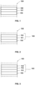
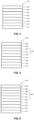
- the present invention relates to an organic compound of formula 1, suitable for use as a layer material for electronic devices, and it relates to an organic semiconductor layer comprising at least one compound thereof, as well as to an organic electronic device comprising at least one organic semiconductor layer, and a method of manufacturing the same.
- Organic electronic devices such as organic light-emitting diodes OLEDs, which are self-emitting devices, have a wide viewing angle, excellent contrast, quick response, high brightness, excellent operating voltage characteristics, and color reproduction.
- a typical OLED comprises an anode, a hole transport layer HTL, an emission layer EML, an electron transport layer ETL, and a cathode, which are sequentially stacked on a substrate.
- the HTL, the EML, and the ETL are thin films formed from organic compounds.
- Performance of an organic light emitting diode may be affected by characteristics of the organic semiconductor layer, and among them, may be affected by characteristics of an organic material of the organic semiconductor layer.
- An aspect of the present invention provides a compound of formula 1: wherein
- H can represent hydrogen or deuterium.
- substituents may be selected from C 1 to C 16 alkyl, C 1 to C 16 alkoxy, C 6 to C 18 aryl, C 3 to C 25 heteroaryl, -PO(R') 2 , D, F or CN, partially or perfluorinated C 1 to C 16 alkyl, partially or perdeuterated C 1 to C 16 alkyl, partially or perfluorinated C 1 to C 16 alkoxy, partially or perdeuterated C 1 to C 16 alkoxy, wherein R' is independently selected from alkyl, aryl or heteroaryl.
- substituents may be selected from C 6 to C 18 aryl, C 3 to C 25 heteroaryl, -PO(R') 2 , D, F or CN, partially or perfluorinated C 1 to C 16 alkyl, C 1 to C 16 alkoxy, partially or perfluorinated C 1 to C 16 alkoxy, partially or perdeuterated C 1 to C 16 alkoxy.
- substituents may be selected from C 6 to C 12 aryl, C 3 to C 17 heteroaryl, -PO(R') 2 , D, F or CN, C 1 to C 6 alkyl, partially or perfluorinated C 1 to C 6 alkyl, partially or perdeuterated C 1 to C 6 alkyl, C 1 to C 6 alkoxy, partially or perfluorinated C 1 to C 6 alkoxy, partially or perdeuterated C 1 to C 6 alkoxy.
- R' may be independently selected from H, C 1 to C 16 alkyl, substituted or unsubstituted C 6 to C 18 aryl, or substituted or unsubstituted C 3 to C 25 heteroaryl, wherein the substituents are selected from D, F or CN, C 1 to C 16 alkyl, partially or perfluorinated C 1 to C 16 alkyl, partially or perdeuterated C 1 to C 16 alkyl, C 1 to C 16 alkoxy, partially or perfluorinated C 1 to C 16 alkoxy, partially or perdeuterated C 1 to C 16 alkoxy.
- R' may be independently selected from H, C 1 to C 6 alkyl, substituted or unsubstituted C 6 to C 12 aryl, or substituted or unsubstituted C 3 to C 17 heteroaryl, wherein the substituents are selected from D, F or CN, C 1 to C 6 alkyl, partially or perfluorinated C 1 to C 6 alkyl, partially or perdeuterated C 1 to C 6 alkyl, C 1 to C 6 alkoxy, partially or perfluorinated C 1 to C 6 alkoxy, partially or perdeuterated C 1 to C 6 alkoxy.
- the heteroatom of the heteroaryl and heteroarylene can be selected from N, O, S, B, Si, P, Se, preferably from N, O and S.
- the heteroatom may be preferably selected from N, if not otherwise defined.
- a 6-member heteroaryl ring and/or 6-member heteroarylene ring comprises as a hetero-atom at least one to three N.
- a 5-member heteroaryl ring and/or 5-member heteroarylene ring comprises as a hetero-atom at least one atom selected from O, S and Se, preferred O or S and more preferred O.
- the compound of formula 1 may comprises 6 to 14 six-member aromatic rings.
- the compound of formula 1 wherein the compound of formula 1 may comprises 7 to 13 six-member aromatic rings.
- the compound of formula 1 may comprises 8 to 12 six-member aromatic rings.
- the compound of formula 1 may comprises 9 to 11 six-member aromatic rings.
- the compound of formula 1 may comprises 8 to 11 six-member aromatic rings.
- the compound of formula 1 may comprises 8, 9, 10, or 11 six-member aromatic rings.
- the compound of formula 1 may comprises 8 to 11 six-member aromatic rings, and at least one six-member aromatic ring comprises an N-atom.
- the compound of formula 1 may comprises 6 to 14 six-member aromatic rings, and at least one 5-member ring.
- the compound of formula 1 may comprises 8 to 11 six-member aromatic rings, and at least one 5-member ring.
- the compound of formula 1 may comprises at least one six-member aromatic ring substituted with CN.
- the compound of formula 1 may comprises at least one six-member aromatic ring substituted with C 1 to C 6 -dialkyl phosphine oxide and preferably substituted with dimethyl phospine oxide group.
- the compound of formula 1 may comprises at least one hetero five-member ring with a heteroatom selected from O or S.
- the compound of formula 1 may comprises at least one 6-member heteroaryl ring comprises 2 N-atoms to 3 N-atoms, preferably 3 N-atoms.
- the compound of formula 1 wherein the compound of formula 1 may comprises at least two 6-member heteroaryl rings comprises 2 N-atoms to 3 N-atoms, preferably 3 N-atoms.
- the compound of formula 1 wherein the compound of formula 1 may comprises at least three 6-member heteroaryl rings comprises 2 N-atoms to 3 N-atoms, preferably 3 N-atoms.
- the compound of formula 1 wherein the compound of formula 1 may comprises at least four 6-member heteroaryl rings comprises 2 N-atoms to 3 N-atoms, preferably 3 N-atoms.
- the compound of formula 1 may comprises at least one 5-member heteroaryl ring comprises O as the hetero atom.
- the compound of formula 1 may comprises at least one 5-member heteroaryl ring comprises S as the hetero atom.
- the compound of formula 1 wherein the compound of formula 1 may comprises at least one 5-member heteroaryl ring comprises Se as the hetero atom.
- the compound of formula 1 wherein the compound of formula 1 may comprises at least two 5-member heteroaryl rings comprises O as the hetero atom.
- the compound of formula 1 wherein the compound of formula 1 may comprises at least two 5-member heteroaryl rings comprises S as the hetero atom.
- a, b, c, d and e are independently 0, 1 or 2, wherein at least two of a, b, c or d is 1 or 2.
- a, b, c, d and e are independently 0, 1 or 2, wherein at least two of a, b, c or d is 1.
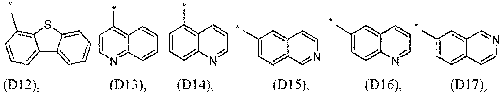
- R 1 , R 2 , R 3 and R 4 are independently selected from substituted or unsubstituted heteroaryl selected from a group comprising of pyridine, pyrimidine, triazine, quinoline, quinoxaline, benzo acridine, dibenzo acridine, phenanthroline, carbazole, dibenzofurane, dibenzothiophene.
- R 1 and R 3 , or R 2 and R 4 , or R 1 and R 4 , orR 2 and R 4 are independently selected from substituted or unsubstituted heteroaryl selected from a group comprising of pyridine, pyrimidine, triazine, quinoline, quinoxaline, benzo acridine, dibenzo acridine, phenanthroline, carbazole, dibenzofurane, dibenzothiophene.
- R 1 and R 3 are independently selected from substituted or unsubstituted heteroaryl selected from a group comprising of pyridine, pyrimidine, triazine, quinoline, quinoxaline, benzo acridine, dibenzo acridine, phenanthroline, carbazole, dibenzofurane, dibenzothiophene; and R 2 and R 4 are hydrogen.
- R 2 and R 3 are independently selected from substituted or unsubstituted heteroaryl selected from a group comprising of pyridine, pyrimidine, triazine, quinoline, quinoxaline, benzo acridine, dibenzo acridine, phenanthroline, carbazole, dibenzofurane, dibenzothiophene; and R 1 and R 4 are hydrogen.
- R 1 , R 2 , R 3 and R 4 is selected from substituted or unsubstituted heteroaryl selected from a group comprising of pyridine, pyrimidine, triazine, quinoline, quinoxaline, benzo acridine, dibenzo acridine, phenanthroline, carbazole, dibenzofurane, dibenzothiophene; and the other are hydrogen.
- the compound of formula 1 may comprises at least three to six phenyl rings that are part of a fused ring system.
- the compound of formula 1 may comprises at least 3 to 10 phenyl rings that are part of a fused ring system, or at least 5 to 8 phenyl rings that are part of a fused ring system.
- R 1 , R 2 , R 3 and R 4 are selected same when a+b+c+d ⁇ 2, preferably R 1 and R 2 or R 3 and R 4 are selected same when a+b+c+d ⁇ 2, further preferred R 1 and R 3 or R 2 and R 4 are selected same when a+b+c+d ⁇ 2.
- R 1 , R 2 , R 3 and R 4 are independently selected from H, nitrile, phenyl, naphthyl, biphenyl, pyridinyl, dibenzofuran, dibenzothiophene or carbazole; preferably at least one of R 1 , R 2 , R 3 or R 4 is independently selected from nitrile, phenyl, naphthyl, biphenyl, pyridinyl, dibenzofuran, dibenzothiophene or carbazole; preferably at least two of R 1 , R 2 , R 3 and R 4 are independently selected from nitrile, phenyl, naphthyl, biphenyl, pyridinyl, dibenzofuran, dibenzothiophene or carbazole; further preferred at least three of R 1 , R 2 , R 3 and R 4 are independently selected from nitrile, phenyl, naphthyl, bipheny
- R 1 , R 2 , R 3 or R 4 is H; preferably at most two of R 1 , R 2 , R 3 and R 4 are H; and more preferred at most three of R 1 , R 2 , R 3 and R 4 are H.
- R 1 , R 2 , R 3 and R 4 are formula 2, preferably one of R 1 , R 2 , R 3 or R 4 is formula 2.
- Ar 1 is selected from substituted or unsubstituted phenylene, biphenylene, terphenylene, naphthylene, phenanthrylene, triphenylene, anthracenylene, wherein the substituents are selected from C 6 to C 18 aryl, C 3 to C 25 heteroaryl, -PO(R') 2 , D, F or CN, partially or perfluorinated C 1 to C 16 alkyl, C 1 to C 16 alkoxy, partially or perfluorinated C 1 to C 16 alkoxy, partially or perdeuterated C 1 to C 16 alkoxy.
- Ar 2 is selected from substituted or unsubstituted aryl selected from a group consisting of anthracenyl, fluoranthenyl, pyrenyl, substituted or unsubstituted heteroaryl selected from a group consisting of pyridine, pyrimidine, triazine, quinoline, quinoxaline, benzoacridine, dibenzoacridine, phenanthroline, carbazole, dibenzofurane, dibenzothiophene, wherein the substituents are selected from C 6 to C 18 aryl, C 3 to C 25 heteroaryl, -PO(R') 2 , D, F or CN, partially or perfluorinated C 1 to C 16 alkyl, C 1 to C 16 alkoxy, partially or perfluorinated C 1 to C 16 alkoxy, partially or perdeuterated C 1 to C 16 alkoxy.
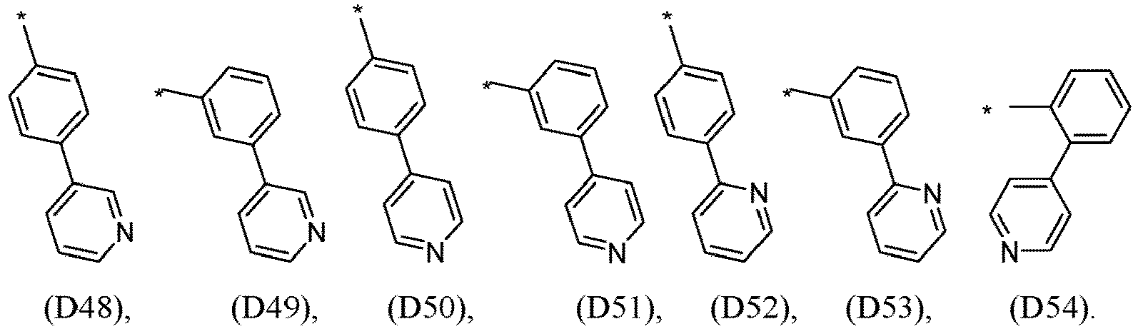
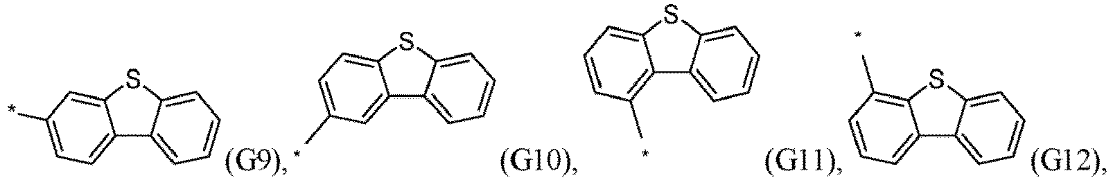
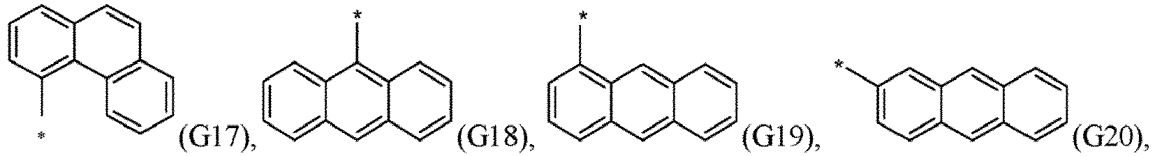
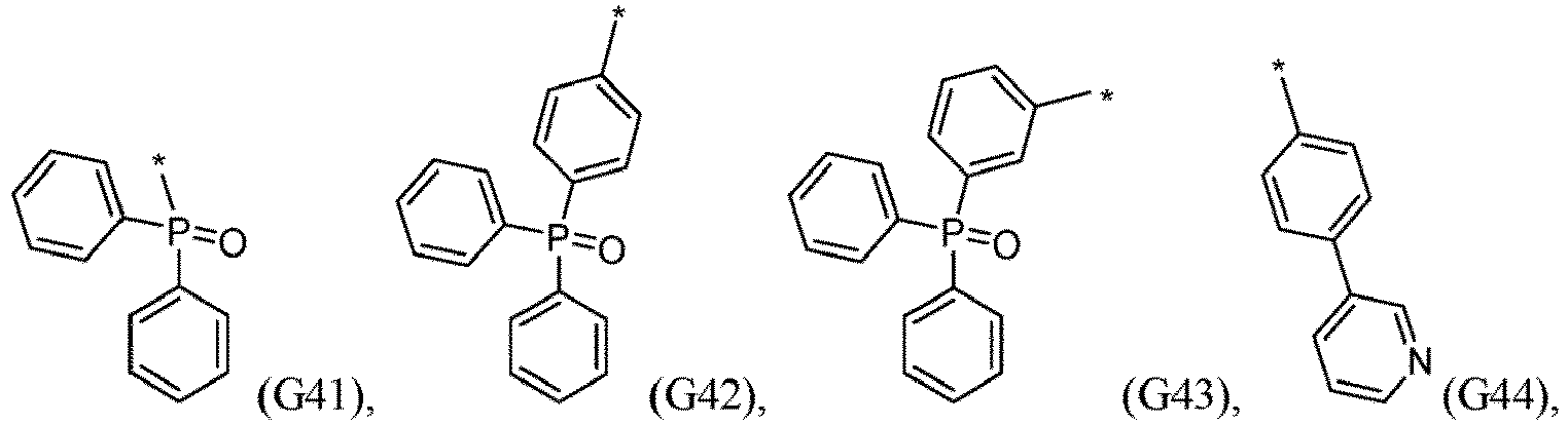
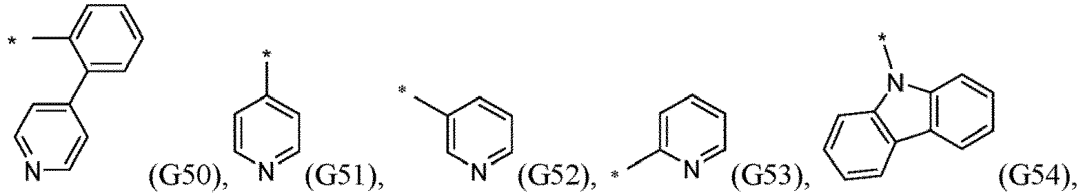
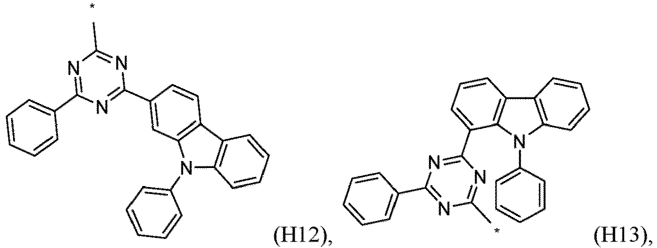
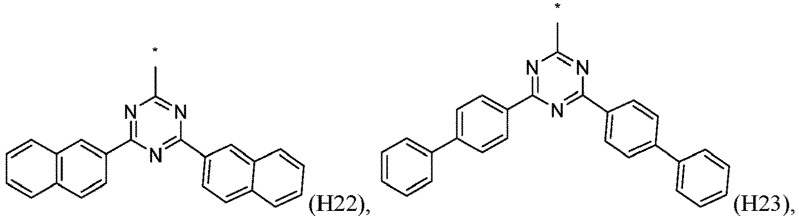
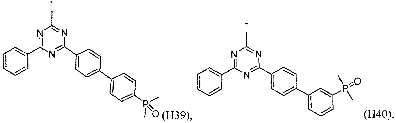
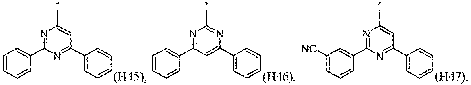
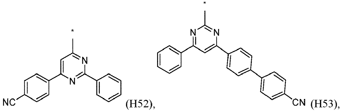
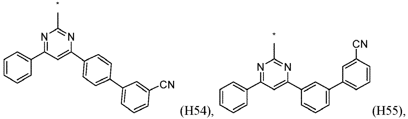
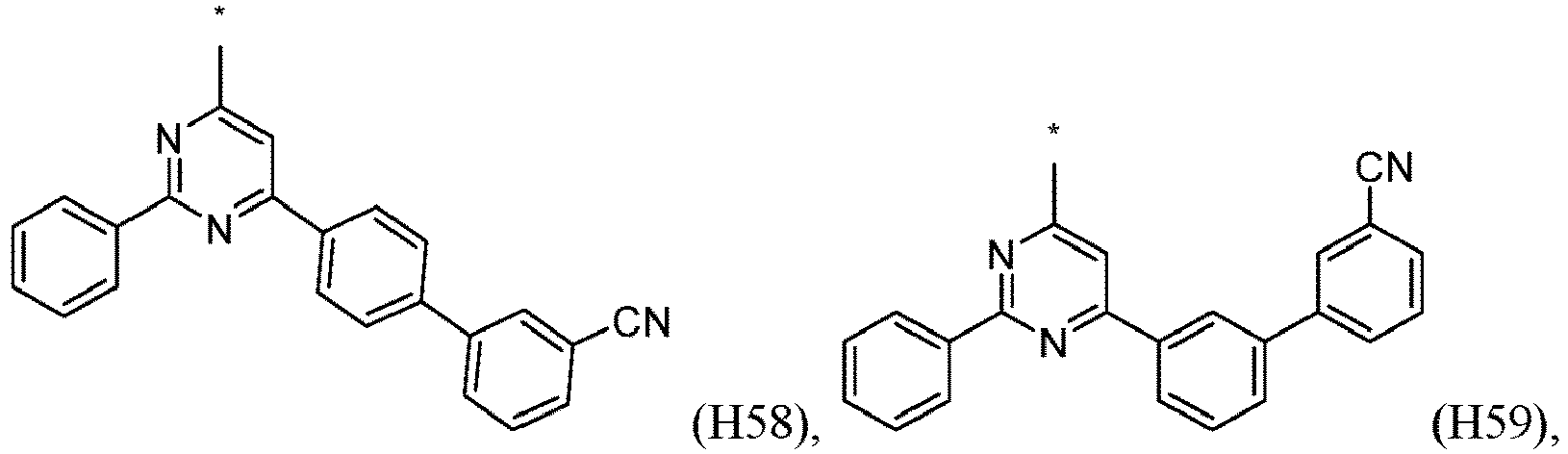
- R 1 , R 2 , R 3 and R 4 are independently selected from hydrogen, CN, or D1 to D54:
- R 5 , R 6 , R 7 , R 8 , R 9 , R 10 , R 11 , R 12 , R 13 , R 14 are independently selected from G1 to G72:
- the compound of formula 1 can be used as a matrix material for a dopant material.
- an organic semiconductor layer may comprises at least one compound of formula 1.
- the layer material can be an organic semiconductor layer, which is used for an organic electronic device.
- the organic electronic device can be an OLED or there like.
- the compounds represented by formula 1 may have strong electron transport characteristics to increase charge mobility and/or stability and thereby to improve luminance efficiency, voltage characteristics, and/or lifetime characteristics.
- the compounds represented by formula 1 may have high electron mobility and a low operating voltage.
- ETL electron transport layer
- the compounds represented by formula 1 and an organic semiconductor layer comprising or consisting of a compound of formula 1 may be non-emissive.
- non-emissive means that the contribution of the compound or layer to the visible emission spectrum from the device is less than 10 %, preferably less than 5 % relative to the visible emission spectrum.
- the visible emission spectrum is an emission spectrum with a wavelength of ⁇ 380 nm to ⁇ 780 nm.
- the compound of formula 1 and the organic semiconductor layer comprising or consisting of the compound of formula 1 is essentially non-emissive or non-emitting.
- the operating voltage also named U, is measured in Volt (V) at 10 milliAmpere per square be centimeter (mA/cm2).
- the candela per Ampere efficiency also named cd/A efficiency, is measured in candela per ampere at 10 milliAmpere per square centimeter (mA/cm2).
- the color space is described by coordinates CIE-x and CIE-y (International Commission on Illumination 1931).
- CIE-x International Commission on Illumination 1931
- CIE-y International Commission on Illumination 1931
- a smaller CIE-y denotes a deeper blue color.
- the highest occupied molecular orbital, also named HOMO, and lowest unoccupied molecular orbital, also named LUMO, are measured in electron volt (eV).
- the rate onset temperature T RO is measured in °C and describes the VTE source temperature at which measurable evaporation of a compound commences at a pressure of less than 10 -5 mbar.
- OLED organic light emitting diode
- organic light emitting device organic optoelectronic device
- organic light-emitting diode organic light-emitting diode
- transition metal means and comprises any element in the d-block of the periodic table, which comprises groups 3 to 12 elements on the periodic table.
- group III to VI metal means and comprises any metal in groups III to VI of the periodic table.
- weight percent As used herein, “weight percent”, “wt.-%”, “percent by weight”, “% by weight”, and variations thereof refer to a composition, component, substance or agent as the weight of that composition, component, substance or agent of the respective electron transport layer divided by the total weight of the composition thereof and multiplied by 100. It is understood that the total weight percent amount of all components, substances or agents of the respective electron transport layer may be selected such that it does not exceed 100 wt.-%.
- volume percent As used herein, “volume percent”, “vol.-%”, “percent by volume”, “% by volume”, and variations thereof refer to an elemental metal, a composition, component, substance or agent as the volume of that elemental metal, component, substance or agent of the respective electron transport layer divided by the total volume of the respective electron transport layer thereof and multiplied by 100. It is understood that the total volume percent amount of all elemental metal, components, substances or agents of the respective cathode electrode layer may be selected such that it does not exceed 100 vol.-%.
- the anode electrode and cathode electrode may be described as anode electrode / cathode electrode or anode electrode / cathode electrode or anode electrode layer / cathode electrode layer.
- an organic optoelectronic device comprises an anode layer and a cathode layer facing each other and at least one organic semiconductor layer between the anode layer and the cathode layer, wherein the organic semiconductor layer comprises or consists of the compound of formula 1.
- a display device comprising the organic electronic device, which can be an organic optoelectronic device, is provided.
- an "alkyl group” may refer to an aliphatic hydrocarbon group.
- the alkyl group may refer to "a saturated alkyl group” without any double bond or triple bond.
- the alkyl group may be a linear, cyclic or branched alkyl group.
- alkyl group includes C 1 to C 16 alkyl, C 3 to C 16 branched alkyl, and C 3 to C 16 cyclic alkyl.
- the alkyl group may be a C 1 to C 16 alkyl group, or preferably a C 1 to C 12 alkyl group. More specifically, the alkyl group may be a C 1 to C 14 alkyl group, or preferably a C 1 to C 10 alkyl group or a C 1 to C 6 alkyl group.
- a C 1 to C 4 alkyl group comprises 1 to 4 carbons in alkyl chain, and may be selected from methyl, ethyl, propyl, iso-propyl, n-butyl, iso-butyl, sec-butyl, and t-butyl.
- alkyl group may be a methyl group, an ethyl group, a propyl group, an isopropyl group, a butyl group, an isobutyl group, a tert-butyl group, a pentyl group, a hexyl group, a cyclopropyl group, a cyclobutyl group, a cyclopentyl group, a cyclohexyl group, and the like.
- arylene group may refer to a group comprising at least one hydrocarbon aromatic moiety, and all the elements of the hydrocarbon aromatic moiety may have p-orbitals which form conjugation, for example a phenyl group, a naphthyl group, an anthracenyl group, a phenanthrenyl group, a pyrenyl group, a fluorenyl group and the like, if not otherwise defined.
- heteroarylene may refer to aromatic heterocycles with at least one heteroatom, and all the elements of the hydrocarbon heteroaromatic moiety may have p-orbitals which form conjugation, if not otherwise defined.
- heteroarylene may refer to antiaromatic heterocycles with at least one heteroatom, for examples azepines.
- the melting point (mp) is determined as peak temperatures from the DSC curves of the above TGA-DSC measurement or from separate DSC measurements (Mettler Toledo DSC822e, heating of samples from room temperature to completeness of melting with heating rate 10 K/min under a stream of pure nitrogen. Sample amounts of 4 to 6 mg are placed in a 40 ⁇ L Mettler Toledo aluminum pan with lid, a ⁇ 1 mm hole is pierced into the lid).
- the compound of formula 1 may have a melting point of ⁇ 305° C and ⁇ 400° C, preferably ⁇ 310° C and ⁇ 370° C, further preferred ⁇ 315° C and ⁇ 360° C.
- the glass transition temperature is measured under nitrogen and using a heating rate of 10 K per min in a Mettler Toledo DSC 822e differential scanning calorimeter as described in DIN EN ISO 11357, published in March 2010.
- the compound of formula 1 may have a glass transition temperature Tg of ⁇ 115° C and ⁇ 280° C, preferably ⁇ 130° C and ⁇ 250° C, further preferred ⁇ 135° C and ⁇ 220° C, in addition preferred ⁇ 140° C and ⁇ 190° C.
- the rate onset temperature T RO is determined by loading 100 mg compound into a VTE source.
- VTE source a point source for organic materials is used as supplied by Kurt J. Lesker Company ( www.lesker.com ) or CreaPhys GmbH ( http://www.creaphys.com ).
- the VTE source is heated at a constant rate of 15 K/min at a pressure of less than 10 -5 mbar and the temperature inside the source measured with a thermocouple. Evaporation of the compound is detected with a QCM detector which detects deposition of the compound on the quartz crystal of the detector. The deposition rate on the quartz crystal is measured in ⁇ ngstrom per second. To determine the rate onset temperature, the deposition rate is plotted against the VTE source temperature. The rate onset is the temperature at which noticeable deposition on the QCM detector occurs. For accurate results, the VTE source is heated and cooled three time and only results from the second and third run are used to determine the rate onset temperature.
- the rate onset temperature may be in the range of 200° C to 260° C. If the rate onset temperature is below 200° C the evaporation may be too rapid and therefore difficult to control. If the rate onset temperature is above 260° C the evaporation rate may be too low which may result in low tact time and decomposition of the organic compound in VTE source may occur due to prolonged exposure to elevated temperatures.
- the rate onset temperature is an indirect measure of the volatility of a compound. The higher the rate onset temperature the lower is the volatility of a compound.
- the compound of formula 1 may have a rate onset temperature T RO of ⁇ 200° C and ⁇ 350° C, preferably ⁇ 220° C and ⁇ 350° C, further preferred ⁇ 250° C and ⁇ 300° C.
- the dipole moment is determined by a semi-empirical molecular orbital method.
- the geometries of the molecular structures are optimized using the hybrid functional B3LYP with the 6-31G* basis set in the gas phase as implemented in the program package TURBOMOLE V6.5 (TURBOMOLE GmbH, Litzenhardtstrasse 19, 76135 Düsseldorf, Germany). If more than one conformation is viable, the conformation with the lowest total energy may be selected to determine the bond lengths of the molecules.
- the compounds according to formula 1 may have a dipole moment (Debye) in the range from ⁇ 0.1 to ⁇ 1.50, preferably from ⁇ 0.3 to ⁇ 1.
- Debye dipole moment
- the HOMO and LUMO are calculated with the program package TURBOMOLE V6.5.
- the optimized geometries and the HOMO and LUMO energy levels of the molecular structures are determined by applying the hybrid functional B3LYP with a 6-31G* basis set in the gas phase. If more than one conformation is viable, the conformation with the lowest total energy may be selected.
- the compounds according to formula 1 may have a HOMO energy level (eV) in the range from -6.00 eV to -4.50 eV, preferably from -5.85 eV to -5.00 eV.
- eV HOMO energy level
- the compounds according to formula 1 may have a LUMO energy level (eV) in the range from -2.30 eV to -1.70 eV, preferably from -1.8 eV to - 2.2 eV.
- eV LUMO energy level
- MM molar mass of a compound in g/mol
- M u the standard atomic weight (namely, the standard relative atomic mass) of the atoms which form the compound multiplied by the molar mass constant
- the compounds according to formula 1 may have a molar mass (g/mol) in the range from 600 g/mol, to 1800 g/mol, preferably from 650 to 1600 g/mol, further preferred from 700 g/mol, to 1500 g/mol.
- the higher glass transition temperature of the compounds according to formula 1 have the benefit for improved properties in high temperature applications, as the morphology of the organic semiconductor layer is less likely to deteriorate.
- the compounds according to formula 1 and the organic electronic devices comprising at least one compound of formula 1 solve the problem underlying the present invention by being superior over the organic electroluminescent devices and compounds known in the art, in particular with respect to operating voltage, which is important for reducing power consumption and increasing battery life, for example of a mobile display device.
- the cd/A efficiency also referred to as current efficiency is kept at a similar or even improved level. Long lifetime at high current density is important for the longevity of a device which is run at high brightness.
- the inventors have surprisingly found that particular good performance can be achieved when using the organic electroluminescent device as a fluorescent blue device.
- organic optoelectronic device having high efficiency and/or long lifetime may be realized.
- a material for the anode may be a metal or a metal oxide, or an organic material, preferably a material with work function above 4.8 eV, more preferably above 5.1 eV, most preferably above 5.3 eV.
- Preferred metals are noble metals like Pt, Au or Ag, preferred metal oxides are transparent metal oxides like ITO or IZO which may be advantageously used in bottom-emitting OLEDs having a reflective cathode.
- the anode may have a thickness from 50 nm to 100 nm, whereas semitransparent metal anodes may be as thin as from 5 nm to 15 nm, and non-transparent metal anodes may have a thickness from 15 nm to 150nm.
- HIL Hole injection layer
- the hole injection layer may improve interface properties between the anode and an organic material used for the hole transport layer, and is applied on a non-planarized anode and thus may planarize the surface of the anode.
- the hole injection layer may include a material having a median value of the energy level of its highest occupied molecular orbital (HOMO) between the work function of the anode material and the energy level of the HOMO of the hole transport layer, in order to adjust a difference between the work function of the anode and the energy level of the HOMO of the hole transport layer.
- HOMO highest occupied molecular orbital
- the hole injection layer may be formed on the anode by any of a variety of methods, for example, vacuum deposition, spin coating, casting, Langmuir-Blodgett (LB) method, or the like.
- vacuum deposition conditions may vary depending on the material that is used to form the hole injection layer, and the desired structure and thermal properties of the hole injection layer to be formed and for example, vacuum deposition may be performed at a temperature of 100 °C to 500 °C, a pressure of 10 -6 Pa to 10 -1 Pa, and a deposition rate of 0.1 to 10 nm/sec, but the deposition conditions are not limited thereto.
- the coating conditions may vary depending on the material that is used to form the hole injection layer, and the desired structure and thermal properties of the hole injection layer to be formed.
- the coating rate may be in the range of 2000 rpm to 5000 rpm
- a temperature at which heat treatment is performed to remove a solvent after coating may be in a range of 80 °C to 200 °C, but the coating conditions are not limited thereto.
- the hole injection layer may further comprise a p-dopant to improve conductivity and/or hole injection from the anode.
- the p-dopant may be homogeneously dispersed in the hole injection layer.
- the p-dopant may be present in the hole injection layer in a higher concentration closer to the anode and in a lower concentration closer to the cathode.
- the p-dopant may be one of a quinone derivative or a radialene compound but not limited thereto.
- the p-dopant are quinone derivatives such as tetracyanoquinonedimethane (TCNQ), 2,3,5,6-tetrafluoro-tetracyano-1,4-benzoquinonedimethane (F4-TCNQ), 4,4',4"-((1E,1'E,1"E)-cyclopropane-1,2,3-triylidenetris(cyanomethanylylidene))-tris(2,3,5,6-tetrafluorobenzonitrile).
- quinone derivatives such as tetracyanoquinonedimethane (TCNQ), 2,3,5,6-tetrafluoro-tetracyano-1,4-benzoquinonedimethane (F4-TCNQ), 4,4',4"-((1E,1'E,
- the device comprising a compound of formula 1 may further comprise a layer comprising a radialene compound and/or a quinodimethane compound.
- the radialene compound and/or the quinodimethane compound may be substituted with one or more halogen atoms and/or with one or more electron withdrawing groups.
- Electron withdrawing groups can be selected from nitrile groups, halogenated alkyl groups, alternatively from perhalogenated alkyl groups, alternatively from perfluorinated alkyl groups.
- Other examples of electron withdrawing groups may be acyl, sulfonyl groups or phosphoryl groups.
- acyl groups, sulfonyl groups and/or phosphoryl groups may comprise halogenated and/or perhalogenated hydrocarbyl.
- the perhalogenated hydrocarbyl may be a perfluorinated hydrocarbyl.
- Examples of a perfluorinated hydrocarbyl can be perfluormethyl, perfluorethyl, perfluorpropyl, perfluorisopropyl, perfluorobutyl, perfluorophenyl, perfluorotolyl; examples of sulfonyl groups comprising a halogenated hydrocarbyl may be trifluoromethylsulfonyl, pentafluoroethylsulfonyl, pentafluorophenylsulfonyl, heptafluoropropylsufonyl, nonafluorobutylsulfonyl, and like.
- the radialene and/or the quinodimethane compound may be comprised in a hole injection, hole transporting and/or a hole generation layer.
- the radialene compound may have formula (XX) and/or the quinodimethane compound may have formula (XXIa) or (XXIb): wherein R 1" , R 2" , R 3 , R 4 , R 5 , R 6 , R 7 , R 8 , R 11 , R 12 , R 15 , R 16 , R 20 , R 21 are independently selected from an electron withdrawing groups and R 9 , R 10 , R 13 , R 14 , R 17 , R 18 , R 19 , R 22 , R 23 and R 24 are independently selected from H, halogen and electron withdrawing groups. Electron withdrawing group that can be suitable used are above mentioned.
- HTL Hole transport layer
- Conditions for forming the hole transport layer and the electron blocking layer may be defined based on the above-described formation conditions for the hole injection layer.
- a thickness of the hole transport part of the charge transport region may be from 10 nm to 1000 nm, for example, 10 nm to 100 nm.
- a thickness of the hole injection layer may be from 10 nm to 1000 nm, for example 10 nm to 100 nm and a thickness of the hole transport layer may be from 5 nm to 200 nm, for example 10 nm to 150 nm.
- Hole transport matrix materials used in the hole transport region are not particularly limited. Preferred are covalent compounds comprising a conjugated system of at least 6 delocalized electrons, preferably organic compounds comprising at least one aromatic ring, more preferably organic compounds comprising at least two aromatic rings, even more preferably organic compounds comprising at least three aromatic rings, most preferably organic compounds comprising at least four aromatic rings.
- Typical examples of hole transport matrix materials which are widely used in hole transport layers are polycyclic aromatic hydrocarbons, triarylene amine compounds and heterocyclic aromatic compounds. Suitable ranges of frontier orbital energy levels of hole transport matrices useful in various layer of the hole transport region are well-known.
- the preferred values may be in the range 0.0 - 1.0 V, more preferably in the range 0.2 - 0.7 V, even more preferably in the range 0.3 - 0.5 V.
- the hole transport part of the charge transport region may further include a buffer layer.
- Buffer layer that can be suitable used are disclosed in US 6 140 763 , US 6 614 176 and in US2016/248022 .
- the buffer layer may compensate for an optical resonance distance of light according to a wavelength of the light emitted from the EML, and thus may increase efficiency.
- Emission layer Emission layer
- the emission layer may be formed on the hole transport region by using vacuum deposition, spin coating, casting, LB method, or the like.
- the conditions for deposition and coating may be similar to those for the formation of the hole injection layer, though the conditions for the deposition and coating may vary depending on the material that is used to form the emission layer.
- the emission layer may include an emitter host (EML host) and an emitter dopant (further only emitter).
- a thickness of the emission layer may be 100 ⁇ to 1000 ⁇ , for example 200 ⁇ to 600 ⁇ . When the thickness of the emission layer is within these ranges, the emission layer may have improved emission characteristics without a substantial increase in operating voltage.
- the emission layer comprises compound of formula 1 as emitter host.
- the emitter host compound has at least three aromatic rings, which are independently selected from carbocyclic rings and heterocyclic rings.
- Ar 111 and Ar 112 may be each independently a substituted or unsubstituted C 6 -C 60 arylene group;
- Ar 113 to Ar 116 may be each independently a substituted or unsubstituted C 1 -C 10 alkyl group or a substituted or unsubstituted C 6 -C 60 arylene group;
- g, h, i, and j may be each independently an integer from 0 to 4.
- Arm and Ar 112 in formula 400 may be each independently one of a phenylene group, a naphthalene group, a phenanthrenylene group, or a pyrenylene group; or a phenylene group, a naphthalene group, a phenanthrenylene group, a fluorenyl group, or a pyrenylene group, each substituted with at least one of a phenyl group, a naphthyl group, or an anthryl group.
- g, h, i, and j may be each independently an integer of 0, 1, or 2.
- Ar 113 to Ar 116 may be each independently one of
- X may be selected form an oxygen atom and a sulfur atom, but embodiments of the invention are not limited thereto.
- any one of R 11 to R 14 is used for bonding to Arm.
- R 11 to R 14 that are not used for bonding to Arm and R 15 to R 20 are the same as R 1 to R 8 .
- any one of R 21 to R 24 is used for bonding to Arm.
- R 21 to R 24 that are not used for bonding to Arm and R 25 to R 30 are the same as R 1 to R 8 .
- the EML host comprises between one and three heteroatoms selected from the group comprising of N, O or S. More preferred the EML host comprises one heteroatom selected from S or O.
- the dopant is mixed in a small amount to cause light emission, and may be generally a material such as a metal complex that emits light by multiple excitation into a triplet or more.
- the dopant may be, for example an inorganic, organic, or organic/inorganic compound, and one or more kinds thereof may be used.
- the emitter may be a red, green, or blue emitter.
- the dopant may be a fluorescent dopant, for example ter-fluorene, the structures are shown below.
- a fluorescent dopant for example ter-fluorene
- DPAVBI 4.4'-bis(4-diphenyl amiostyryl)biphenyl
- TBPe 2,5,8,11-tetra-tert-butyl perylene
- Compound 8 are examples of fluorescent blue dopants.
- the dopant may be a phosphorescent dopant, and examples of the phosphorescent dopant may be an organic metal compound comprising Ir, Pt, Os, Ti, Zr, Hf, Eu, Tb, Tm, Fe, Co, Ni, Ru, Rh, Pd, or a combination thereof.
- the phosphorescent dopant may be, for example a compound represented by formula Z, but is not limited thereto: J 2 MX (Z).
- M is a metal
- J and X are the same or different, and are a ligand to form a complex compound with M.
- the M may be, for example Ir, Pt, Os, Ti, Zr, Hf, Eu, Tb, Tm, Fe, Co, Ni, Ru, Rh, Pd or a combination thereof, and the J and X may be, for example a bidendate ligand.
- One or more emission layers may be arranged between the anode and the cathode. To increase overall performance, two or more emission layers may be present.
- a charge generation layer (also named CGL) may be arranged between the first and the second emission layer, and second and third emission layer, if present.
- the CGL comprises a n-type charge generation layer (also named n-CGL or electron generation layer) and a p-type charge generation layer (also named p-CGL or hole generation layer).
- An interlayer may be arranged between the n-type CGL and the p-type CGL.
- the n-type CGL may comprise a compound of formula 1.
- the n-type CGL further comprises a metal, metal salt or organic metal complex, preferably a metal.
- the metal may be selected from an alkali, alkaline earth or rare earth metal.
- the p-type CGL may comprise a dipyrazino[2,3-f:2',3'-h]quinoxaline, a quinone compound or a radialene compound, preferably dipyrazino[2,3-f:2',3'-h]quinoxaline-2,3,6,7,10,11-hexacarbonitrile or a compound or formula (XX) and/or a compound of formula (XXIa) or (XXIb) as mentioned above.
- the n-type and p-type CGL are in direct contact.
- Electron transport layer ETL
- the organic semiconductor layer that comprises compound of formula 1 is an electron transport layer.
- the electron transport layer may consist of compound of formula 1.
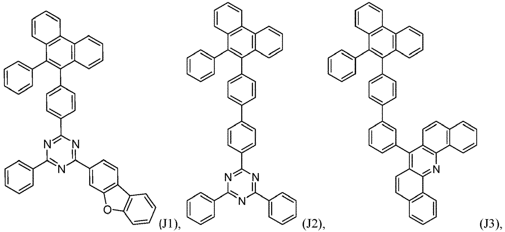
- an organic light emitting diode comprises at least one electron transport layer, and in this case, the electron transport layer comprises at least one compound of formula 1, or preferably of at least one compound of formulae J1 to J53, preferably of J1 or J2.
- the organic electronic device comprises an electron transport region of a stack of organic layers formed by two or more electron transport layers, wherein at least one electron transport layer comprises a compound of formula 1.
- the electron transport layer may include one or two or more different electron transport compounds.
- a first electron transport layer comprises at least one compound of formula 1 according to the invention and a second electron transport layer (ETL2) comprises a matrix compound, which may be selected different to the compound of formula 1 according to the invention, and may be selected from:
- a first electron transport layer comprises at least one compound of formula 1 according to the invention and a second electron transport layer comprises a matrix compound, which may be selected different to the compound of formula 1 according to the invention, and may be selected from a phosphine oxide based compound, preferably (3-(dibenzo[c,h]acridin-7-yl)phenyl)diphenylphosphine oxide and/or phenyl bis(3-(pyren-1-yl)phenyl)phosphine oxide and/or 3-Phenyl-3H-benzo[b]dinaphtho[2,1-d:1',2'-f]phosphepine-3-oxide.
- a phosphine oxide based compound preferably (3-(dibenzo[c,h]acridin-7-yl)phenyl)diphenylphosphine oxide and/or phenyl bis(3-(pyren-1-yl)phenyl)phosphine oxide and/or 3-
- the first electron transport layer may also be described as auxiliary electron transport layer or a hole blocking layer.
- a first and a second electron transport layers comprise compound of formula 1, wherein the compound of formula 1 is not selected the same.
- a second electron transport layer comprises at least one compound of formula 1 according to the invention and a first electron transport layer (ETL1) comprises an azine compound,
- the thickness of the electron transport layer may be from 0.5 nm to 100 nm, for example 2 nm to 40 nm, preferably 2 to 10 nm.
- the thickness of the first electron transport layer may be from 0.5 nm to 100 nm, for example 2 nm to 40 nm, preferably 2 to 10 nm.
- a thickness of an optional second electron transport layer may be 1 nm to 100 nm, for example 2 nm to 50 nm, preferably 10 to 40 nm. When the thickness of the electron transport layer is within these ranges, the electron transport layer may have satisfactory electron transporting ability without a substantial increase in operating voltage.
- the electron transport layer may further comprise a monovalent or divalent metal halide or an organic monovalent or divalent metal complex, preferably an alkali halide and/or alkali organic complex.
- the first and second electron transport layers comprise compound of formula 1, wherein the second electron transport layer further comprises an alkali halide and/or alkali organic complex.
- Alkali halides also known as alkali metal halides, are the family of inorganic compounds with the chemical formula MX, where M is an alkali metal and X is a halogen.
- M can be selected from Li, Na, Potassium, Rubidium and Cesium.
- X can be selected from F, Cl, Br and J.
- a lithium halide may be preferred.
- the lithium halide can be selected from the group comprising LiF, LiCl, LiBr and LiJ. However, most preferred is LiF.
- the alkali halide is essentially non-emissive or non-emissive.
- the alkali organic complex comprises an alkali metal and at least one organic ligand.
- the alkali metal is preferably selected from lithium.
- the organic ligand of the lithium organic complex is a quinolate, a borate, a phenolate, a pyridinolate or a Schiff base ligand;
- the organic ligand of the alkali organic complex preferably of a lithium organic complex
- Quinolates that can be suitable used are disclosed in WO 2013079217 A1 .
- the organic ligand of the lithium organic complex can be a borate based organic ligand,
- the lithium organic complex is a lithium tetra(1H-pyrazol-1-yl)borate.
- Borate based organic ligands that can be suitable used are disclosed in WO 2013079676 A1 .
- the organic ligand of the lithium organic complex can be a phenolate ligand, Preferably the lithium organic complex is a lithium 2-(diphenylphosphoryl)phenolate.
- Phenolate ligands that can be suitable used are disclosed in WO 2013079678 A1 .
- phenolate ligands can be selected from the group of pyridinolate, preferably 2-(diphenylphosphoryl)pyridin-3-olate. Pyridine phenolate ligands that can be suitable used are disclosed in JP 2008195623 .
- phenolate ligands can be selected from the group of imidazol phenolates, preferably 2-(1-phenyl-1H-benzo[d]imidazol-2-yl)phenolate. Imidazol phenolate ligands that can be suitable used are disclosed in JP 2001291593 .
- phenolate ligands can be selected from the group of oxazol phenolates, preferably 2-(benzo[d]oxazol-2-yl)phenolate.
- Oxazol phenolate ligands that can be suitable used are disclosed in US 20030165711 .
- the alkali organic complex may be essentially non-emissive.
- Electron injection layer (EIL)
- the organic electroluminescent device may further comprise an electron injection layer between the electron transport layer (first-ETL) and the cathode.
- the electron injection layer may facilitate injection of electrons from the cathode.
- the electron injection layer comprises:
- the electron injection layer may include at least one selected from LiF, NaCl, CsF, Li 2 O, and BaO.
- a thickness of the EII may be from 0.1 nm to 10 nm, or 0.3 nm to 9 nm. When the thickness of the electron injection layer is within these ranges, the electron injection layer may have satisfactory electron injection ability without a substantial increase in operating voltage.
- the electron injection layer may comprise a compound of formula 1.
- a material for the cathode may be a metal, an alloy, or an electrically conductive compound that have a low work function, or a combination thereof.
- Specific examples of the material for the cathode may be lithium (Li), magnesium (Mg), aluminum (Al), aluminum-lithium (Al-Li), calcium (Ca), magnesium-indium (Mg-In), magnesium-silver (Mg-Ag), silver (Ag) etc.
- the cathode may be formed as a light-transmissive electrode from, for example, indium tin oxide (ITO), indium zinc oxide (IZO) or silver (Ag).
- the cathode may have a thickness from 50 nm to 100 nm, whereas semitransparent metal cathodes may be as thin as from 5 nm to 15 nm.
- a substrate may be further disposed under the anode or on the cathode.
- the substrate may be a substrate that is used in a general organic light emitting diode and may be a glass substrate or a transparent plastic substrate with strong mechanical strength, thermal stability, transparency, surface smoothness, ease of handling, and water resistance.
- first element when a first element is referred to as being formed or disposed "on" a second element, the first element can be disposed directly on the second element, or one or more other elements may be disposed there between.
- first element when referred to as being formed or disposed "directly on” a second element, no other elements are disposed there between.
- contacting sandwiched refers to an arrangement of three layers whereby the layer in the middle is in direct contact with the two adjacent layers.
- the organic light emitting diodes according to an embodiment of the present invention may include a hole transport region; an emission layer; and a first electron transport layer comprising a compound according to formula 1.
- an organic semiconductor layer may comprise at least one compound of formula 1.
- the organic semiconductor layer may comprises at least one compound of formula 1 and further comprises a metal, metal salt or organic alkali metal complex, preferably alkali metal complex, more preferably LiQ or alkali borate.
- the organic semiconductor layer may comprises at least one compound of formula 1 and further comprises a metal, metal salt or organic metal complex, preferably an organic monovalent or divalent metal complex, more preferably LiQ or alkali borate.
- the organic semiconductor layer may comprises at least one compound of formula 1 and LiQ.
- the organic semiconductor layer may comprises at least one compound of formula 1 and alkali borate.
- At least one organic semiconductor layer is arranged between the emission layer and the cathode, preferably between the electron injection layer and the cathode.
- the organic semiconductor layer is a first electron transport layer and it is arranged between the emission layer and the second electron transport layer.
- the organic semiconductor layer is arranged between the first and second emission layer.
- the organic semiconductor layer can be an electron transport layer, an emission layer, a hole blocking layer, a charge generation layer and/or an electron injection layer, preferably an electron transport layer or a charge generation layer, and more preferred an electron transport layer.
- the organic semiconductor layer can be arranged between a photoactive layer and a cathode layer, preferably between an emission layer or light-absorbing layer and the cathode layer, preferably the organic semiconductor layer is an electron transport layer.
- the organic semiconductor layer may comprise at least one alkali halide or alkali organic complex.
- An organic semiconductor layer comprises a compound according to formula 1, 1a or 1b is essentially non-emissive or non-emitting.
- An organic electronic device comprising an anode layer, a cathode layer and at least one organic semiconductor layer according, wherein the at least one organic semiconductor layer comprises a compound of formula 1.
- An organic electronic device which comprises at least one organic semiconductor layer that comprises a compound according to formula 1, wherein this layer is essentially non-emissive or non-emitting.
- the organic electronic device may comprises at least one organic semiconductor layer comprising compound of formula 1 that is an electron transport layer, an emission layer, a hole blocking layer, a charge generation layer and/or an electron injection layer, preferably an electron transport layer or a charge generation layer, more preferred an electron transport layer.
- the organic electronic device may comprises at least one organic semiconductor layer, wherein the organic semiconductor layer comprising compound of formula 1 is arranged between a photoactive layer and a cathode layer, preferably between an emission layer or light-absorbing layer and the cathode layer, preferably the organic semiconductor layer is an electron transport layer
- the organic electronic device may comprises at least one organic semiconductor layer comprising compound of formula 1, wherein the at least one organic semiconductor layer further comprises at least one alkali halide or alkali organic complex.
- An organic electronic device comprises at least one organic semiconductor layer comprising at least one compound of formula 1, at least one anode layer, at least one cathode layer and at least one emission layer, wherein the organic semiconductor layer comprising at least one compound of formula 1 is preferably arranged between the emission layer and the cathode layer.
- An organic electronic device comprises at least one organic semiconductor layer comprising at least one compound of formula 1, at least one anode layer, at least one cathode layer, at least one emission layer and at least one auxiliary electron transport layer, wherein the organic semiconductor layer comprising at least one compound of formula 1 is preferably arranged between the auxiliary electron transport layer and the cathode layer.
- An organic electronic device comprises at least one organic semiconductor layer comprising at least one compound of formula 1 and further comprises at least one alkali halide or alkali organic complex.
- An organic light-emitting diode (OLED) may include an anode, a hole transport layer (HTL), an emission layer (EML), an electron transport layer (ETL) comprising at least one compound of formula 1, and a cathode, which are sequentially stacked on a substrate.
- HTL hole transport layer
- EML emission layer
- ETL electron transport layer
- cathode cathode
- An organic electronic device can be a light emitting device, thin film transistor, a battery, a display device or a photovoltaic cell, and preferably a light emitting device.
- a light emitting device can be an OLED.
- the OLED may have the following layer structure, wherein the layers having the following order: an anode layer, a hole injection layer, optional a first hole transport layer, optional a second hole transport layer, an emission layer, an electron transport layer comprising compound of formula 1 according to the invention, an electron injection layer, and a cathode layer.
- the methods for deposition that can be suitable comprise:
- the method may further include forming on the anode electrode an emission layer and at least one layer selected from the group comprising of forming a hole injection layer, forming a hole transport layer, or forming a hole blocking layer, between the anode electrode and the first electron transport layer.
- the method may further include the steps for forming an organic light-emitting diode (OLED), wherein
- the method may further include forming an electron injection layer on a first electron transport layer.
- the OLED may not comprise an electron injection layer.
- the OLED may have the following layer structure, wherein the layers having the following order: an anode, first hole transport layer, second hole transport layer, emission layer, optional second electron transport layer, first electron transport layer comprising compound of formula 1 according to the invention, optional a second electron transport layer, optional an electron injection layer, and a cathode.
- an electronic device comprising at least one organic light emitting device according to any embodiment described throughout this application, preferably, the electronic device comprises the organic light emitting diode in one of embodiments described throughout this application. More preferably, the electronic device is a display device.
- Example 1 and 2 of compounds J1 and J2 and comparative examples C1 a glass substrate was cut to a size of 50 mm ⁇ 50 mm ⁇ 0.7 mm, ultrasonically cleaned with isopropyl alcohol for 5 minutes and then with pure water for 5 minutes, and cleaned again with UV ozone for 30 minutes. 100 nm Ag were deposited on the glass substrate as anode at a pressure of 10 -5 to 10 -7 mbar to form the anode.
- HTL hole transport layer
- N,N-bis(4-(dibenzo[b,d]furan-4-yl)phenyl)-[1,1':4',1"-terphenyl]-4-amine ( CAS 1198399-61-9 ) was vacuum deposited on the HTL, to form an electron blocking layer (EBL) having a thickness of 5 nm.
- EBL electron blocking layer
- a first electron transport layer (ETL1) is formed on the EML with a thickness of 5 nm by depositing 2,4-diphenyl-6-(4',5',6'-triphenyl-[1,1':2',1":3",1′′′:3′′′,1 ⁇ -quinquephenyl]-3 ⁇ -yl)-1,3,5-triazine on the emission layer with a thickness of 5 nm, see Table 2.
- the second electron transport layer (ETL2) is formed on the first electron transport layer (ETL1) with a thickness of 31 nm by depositing 50 vol.-% of a compound selected from J1 for example 1 and J2 for example 2 of formula 1 as matrix compound and 50 vol.-% of alkali organic complex LiQ, see Table 2; as well as for the comparative example C1 the second electron transport layer is formed on the first electron transport layer with a thickness of 31 nm by depositing 50 vol.-% of the compound of the comparative example C1 as matrix compound and 50 vol.-% of alkali organic complex LiQ, see Table 2.
- the electron injection layer is formed on the electron transporting layer by deposing Yb with a thickness of 2 nm.
- Ag is evaporated at a rate of 0.01 to 1 ⁇ /s at 10 -7 mbar to form a cathode with a thickness of 11 nm.
- a cap layer of Biphenyl-4-yl(9,9-diphenyl-9H-fluoren-2-yl)-[4-(9-phenyl-9H-carbazol-3-yl)phenyl]-amine is formed on the cathode with a thickness of 75 nm.
- the OLED stack is protected from ambient conditions by encapsulation of the device with a glass slide. Thereby, a cavity is formed, which includes a getter material for further protection.
- the current efficiency is measured at 20°C.
- the current-voltage characteristic is determined using a Keithley 2635 source measure unit, by sourcing a voltage in V and measuring the current in mA flowing through the device under test. The voltage applied to the device is varied in steps of 0.1V in the range between 0V and 10V.
- the luminance-voltage characteristics and CIE coordinates are determined by measuring the luminance in cd/m 2 using an Instrument Systems CAS-140CT array spectrometer for each of the voltage values.
- the cd/A efficiency at 10 mA/cm 2 is determined by interpolating the luminance-voltage and current-voltage characteristics, respectively.
- Lifetime LT of the device is measured at ambient conditions (20°C) and 30 mA/cm 2 , using a Keithley 2400 source meter, and recorded in hours.
- the brightness of the device is measured using a calibrated photo diode.
- the lifetime LT is defined as the time till the brightness of the device is reduced to 97 % of its initial value.
- Compound C1 is a state of the art compound. As can be seen in Table 1, the compounds of formula 1 of the example 1, 2 and 3 have a higher melting point and higher glass transition temperature as compared to the comparative example 1. The rate onset temperature is in a range suitable for mass production.
Landscapes
- Chemical & Material Sciences (AREA)
- Organic Chemistry (AREA)
- Physics & Mathematics (AREA)
- Materials Engineering (AREA)
- Engineering & Computer Science (AREA)
- Spectroscopy & Molecular Physics (AREA)
- Life Sciences & Earth Sciences (AREA)
- Molecular Biology (AREA)
- General Health & Medical Sciences (AREA)
- Biochemistry (AREA)
- Health & Medical Sciences (AREA)
- Electroluminescent Light Sources (AREA)
- Nitrogen Condensed Heterocyclic Rings (AREA)
- Plural Heterocyclic Compounds (AREA)
- Organic Low-Molecular-Weight Compounds And Preparation Thereof (AREA)
Claims (20)
- Verbindung gemäß Formel 1:
 R1, R2, R3 und R4 unabhängig ausgewählt sind aus Wasserstoff, substituiertem oder unsubstituiertem C6- bis C38-Aryl, substituiertem oder unsubstituiertem C3- bis C36-Heteroaryl oder C1- bis C16-Alkylgruppe, -PO(R')2, D, F, CN oder Formel 2;
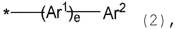
die Substituenten ausgewählt sind aus C6- bis C18-Aryl, C3- bis C25-Heteroaryl, -PO(R')2, D, F oder CN, teilweise oder perfluoriertem C1- bis C16-Alkyl, C1- bis C16-Alkoxy, teilweise oder perfluoriertem C1- bis C16-Alkoxy, teilweise oder perdeuteriertem C1- bis C16-Alkoxy;R' unabhängig ausgewählt ist aus Alkyl, Aryl oder Heteroaryl;a, b, c, d und e unabhängig 0, 1 oder 2 sind, wobei wenigstens eines von a, b, c oder d 1 oder 2 ist; wobei wenigstens eines von R1, R2, R3 und R4 Formel 2 ist,Ar1 ausgewählt ist aus substituiertem oder unsubstituiertem C6- bis C38-Arylen, substituiertem oder unsubstituiertem C3- bis C36-Heteroarylen oder C1- bis C16-Alkylengruppe, wobei
die Substituenten ausgewählt sind aus C6- bis C18-Aryl, C3- bis C25-Heteroaryl, -PO(R')2, D, F oder CN, teilweise oder perfluoriertem C1- bis C16-Alkyl, C1- bis C16-Alkoxy, teilweise oder perfluoriertem C1- bis C16-Alkoxy, teilweise oder perdeuteriertem C1- bis C16-Alkoxy;Ar2 ausgewählt ist aus substituiertem oder unsubstituiertem C6- bis C38-Aryl, substituiertem oder unsubstituiertem C3- bis C36-Heteroaryl oder C1-bis C16-Alkylgruppe, wobeiwobei
die Substituenten ausgewählt sind aus C6- bis C18-Aryl, C3- bis C25-Heteroaryl, -PO(R')2, D, F oder CN, teilweise oder perfluoriertem C1- bis C16-Alkyl, C1- bis C16-Alkoxy, teilweise oder perfluoriertem C1- bis C16-Alkoxy, teilweise oder perdeuteriertem C1- bis C16-Alkoxy;Ar1 nicht einen oder mehrere CN-Substituenten enthält, wenn Ar2 substituiertes oder unsubstituiertes C6- bis C38-Aryl ist;
wobeidie folgende Verbindung 3 ausgeschlossen ist:
- Verbindung der Formel 1 gemäß Anspruch 1, wobei- wenigstens zwei von a, b, c oder d 0, 1 oder 2 sind, vorzugsweise wenigstens zwei von a, b, c oder d 0 oder 1 sind; oder- a und b 0 sind und c oder d unabhängig ausgewählt ist aus 1 oder 2, vorzugsweise a und b 0 sind und c oder d 1 ist; oder- c und d 0 sind und a oder b unabhängig ausgewählt ist aus 1 oder 2, vorzugsweise c und d 0 sind und a oder b 1 ist; oder- a und c 0 sind und b oder d unabhängig ausgewählt ist aus 1 oder 2, vorzugsweise a und c 0 sind und b oder d 1 ist; oder- b und d 0 sind und a oder c unabhängig ausgewählt ist aus 1 oder 2, vorzugsweise b und d 0 sind und a oder c 1 ist; oder- wenigstens drei ausgewählt aus a, b, c und d 0 sind und eines ausgewählt aus a, b, c und d 1 ist; oder- wenigstens drei ausgewählt aus a, b, c und d 1 oder 2 sind, vorzugsweise wenigstens zwei von a, b, c und d 1 sind.
- Verbindung der Formel 1 gemäß Anspruch 1 oder 2, wobei e 0, 1 oder 2, bevorzugter 0 oder 1 und bevorzugter 0 ist.
- Verbindung der Formel 1 gemäß einem der Ansprüche 1 bis 3, wobei wenigstens zwei von R1, R2, R3 und R4 gleich ausgewählt sind, wenn a+b+c+d ≥ 2, vorzugsweise R1 und R2 oder R3 und R4 gleich ausgewählt sind, wenn a+b+c+d ≥ 2, bevorzugter R1 und R3 oder R2 und R4 gleich ausgewählt sind, wenn a+b+c+d ≥ 2.
- Verbindung der Formel 1 gemäß einem der Ansprüche 1 bis 4, wobei R1, R2, R3 und R4 unabhängig ausgewählt sind aus H, Nitril, Phenyl, Naphthyl, Biphenyl, Pyridinyl, Dibenzofuran, Dibenzothiophen und Carbazol; vorzugsweise wenigstens eines von R1, R2, R3 und R4 unabhängig ausgewählt ist aus Nitril, Phenyl, Naphthyl, Biphenyl, Pyridinyl, Dibenzofuran, Dibenzothiophen und Carbazol; vorzugsweise wenigstens zwei von R1, R2, R3 und R4 unabhängig ausgewählt sind aus Nitril, Phenyl, Naphthyl, Biphenyl, Pyridinyl, Dibenzofuran, Dibenzothiophen und Carbazol; bevorzugter wenigstens drei von R1, R2, R3 und R4 unabhängig ausgewählt sind aus Nitril, Phenyl, Naphthyl, Biphenyl, Pyridinyl, Dibenzofuran, Dibenzothiophen und Carbazol; zusätzlich vorzugsweise wenigstens drei von R1, R2, R3 und R4 unabhängig ausgewählt sind aus Nitril, Phenyl, Naphthyl, Biphenyl, Pyridinyl, Dibenzofuran, Dibenzothiophen und Carbazol.
- Verbindung der Formel 1 gemäß einem der Ansprüche 1 bis 5, wobei höchstens eines von R1, R2, R3 und R4 H ist; vorzugsweise höchstens zwei von R1, R2, R3 und R4 H sind; und bevorzugter höchstens drei von R1, R2, R3 und R4 H sind.
- Verbindung der Formel 1 gemäß einem der Ansprüche 1 bis 6, wobei zwei von R1, R2, R3 und R4 Formel 2 sind, vorzugsweise eines von R1, R2, R3 und R4 Formel 2 ist.
- Verbindung der Formel 1 gemäß einem der Ansprüche 1 bis 7, wobei Ar1 ausgewählt ist aus substituiertem oder unsubstituiertem Phenylen, Biphenylen, Terphenylen, Naphthylen, Phenanthrylen, Triphenylen, Anthracenylen, wobei
die Substituenten ausgewählt sind aus C6- bis C18-Aryl, C3- bis C25-Heteroaryl, -PO (R') 2, D, F oder CN, teilweise oder perfluoriertem C1- bis C16-Alkyl, C1-bis C16-Alkoxy, teilweise oder perfluoriertem C1- bis C16-Alkoxy, teilweise oder perdeuteriertem C1- bis C16-Alkoxy. - Verbindung der Formel 1 gemäß einem der Ansprüche 1 bis 8, wobei Ar2 ausgewählt ist aus substituiertem oder unsubstituiertem Aryl ausgewählt aus einer Gruppe bestehend aus Anthracenyl, Fluoranthenyl, Pyrenyl, substituiertem oder unsubstituiertem Heteroaryl ausgewählt aus einer Gruppe bestehend aus Pyridin, Pyrimidin, Triazin, Chinolin, Chinoxalin, Benzoacridin, Dibenzoacridin, Phenanthrolin, Carbazol, Dibenzofuran, Dibenzothiophen, wobei
die Substituenten ausgewählt sind aus C6- bis C18-Aryl, C3- bis C25-Heteroaryl, -PO(R')2, D, F oder CN, teilweise oder perfluoriertem C1- bis C16-Alkyl, C1-bis C16-Alkoxy, teilweise oder perfluoriertem C1- bis C16-Alkoxy, teilweise oder perdeuteriertem C1- bis C16-Alkoxy. - Verbindung der Formel 1 gemäß einem der Ansprüche 1 bis 9, wobei R1, R2, R3 und R4 unabhängig ausgewählt sind aus Wasserstoff, CN oder D1 bis D54:


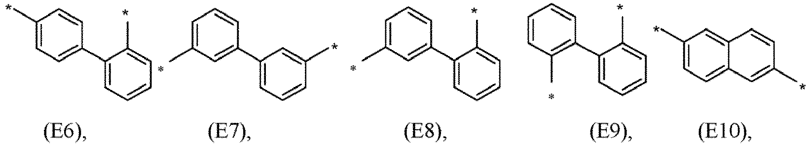
- Verbindung der Formel 1 gemäß einem der Ansprüche 1 bis 10, wobei Ar1 ausgewählt ist aus E1 bis E14:


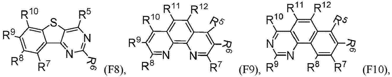
- Verbindung der Formel 1 gemäß einem der Ansprüche 1 bis 11, wobei Ar2 ausgewählt ist aus F1 bis F13:


 R5, R6, R7, R8, R9, R10, R11, R12, R13, R14 unabhängig ausgewählt sind aus Einfachbindung, Wasserstoff, substituiertem oder unsubstituiertem Phenyl, Naphthyl, Biphenyl, Pyridinyl, Dibenzofuryl, Benzofuranyl, Dibenzothienyl, Benzothiophenyl, Anthracenyl, Phenanthryl, Carbazolyl,wobei
die Substituenten ausgewählt sind aus C6- bis C18-Aryl, C3- bis C25-Heteroaryl, -PO(R')2, D, F oder CN, teilweise oder perfluoriertem C1- bis C16-Alkyl, C1- bis C16-Alkoxy, teilweise oder perfluoriertem C1- bis C16-Alkoxy, teilweise oder perdeuteriertem C1- bis C16-Alkoxy; undwobei
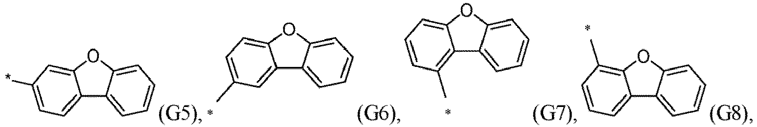
eines von R5, R6, R7, R8, R9, R10, R11, R12, R13, R14 nur eine Einfachbindung darstellt und die Einfachbindung die Einfachbindung ist, die Ar2 an Ar1 bindet. - Verbindung der Formel 1 gemäß einem der Ansprüche 1 bis 12, wobei R5, R6, R7, R8, R9, R10, R11, R12, R13, R14 unabhängig ausgewählt sind aus G1 bis G72:


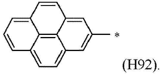
- Verbindung der Formel 1 gemäß einem der Ansprüche 1 bis 13, wobei Ar2 ausgewählt ist aus H1 bis H92:


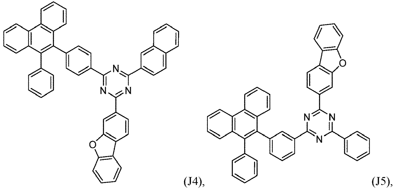
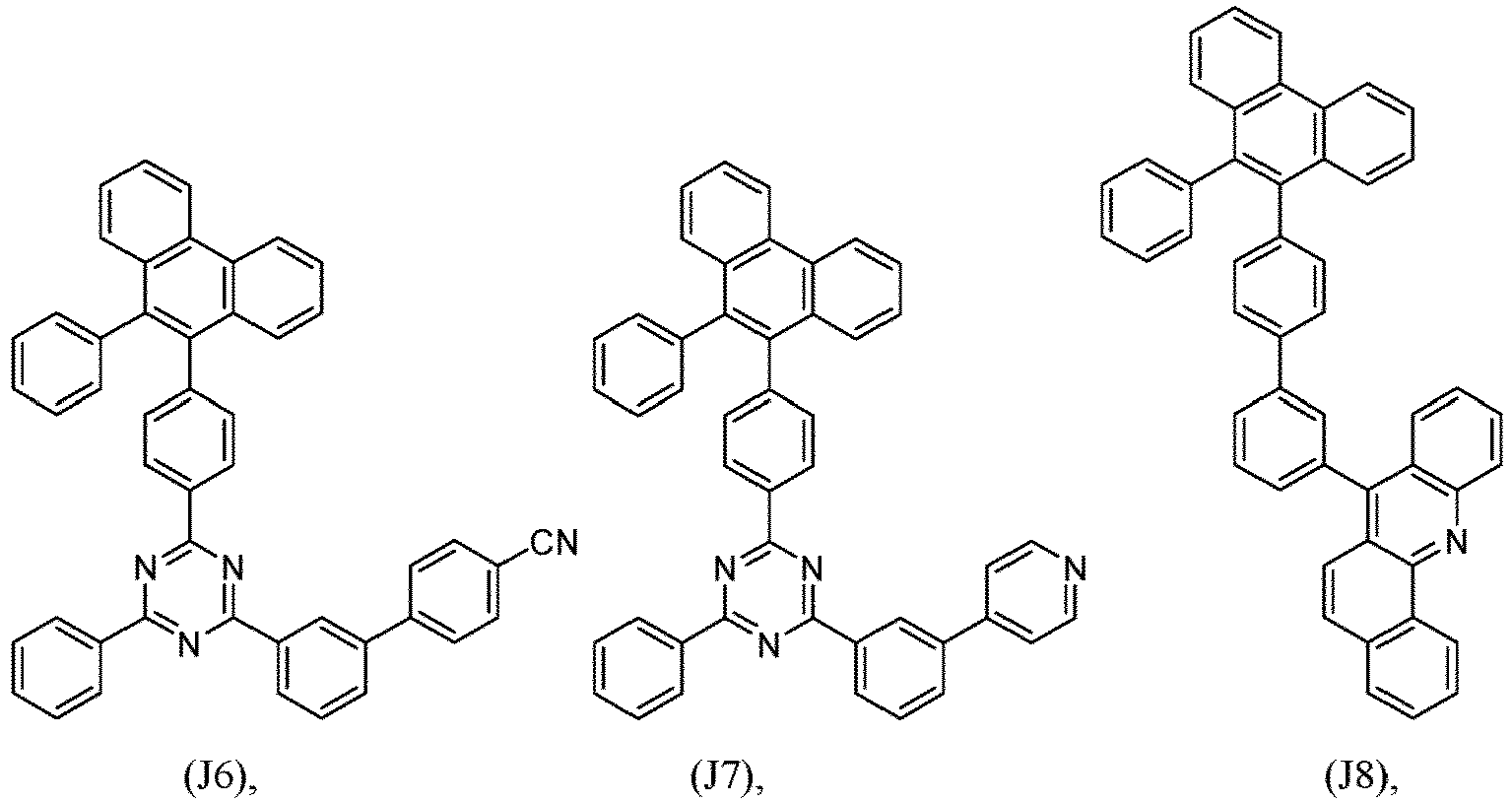
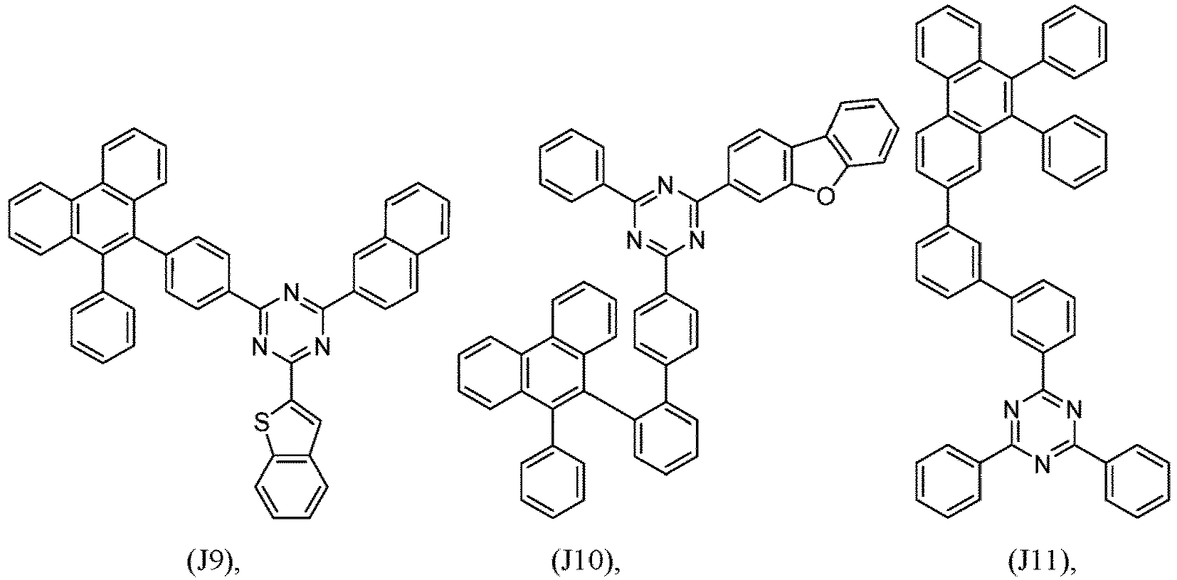
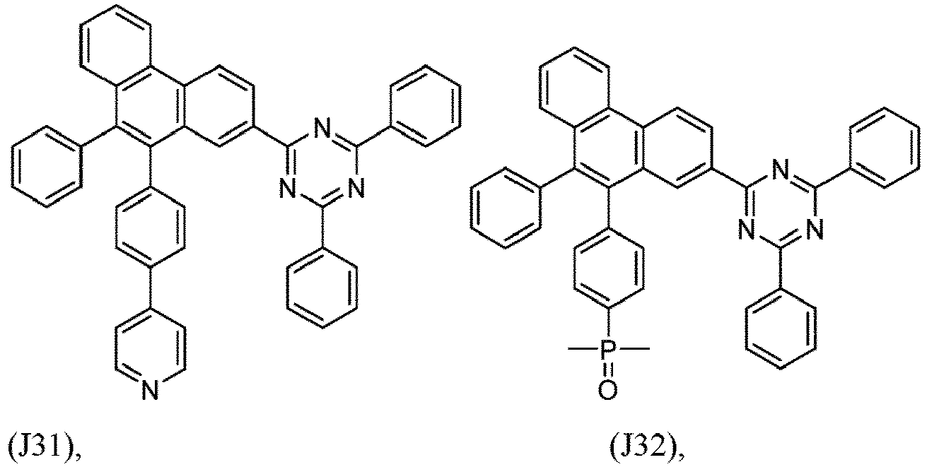
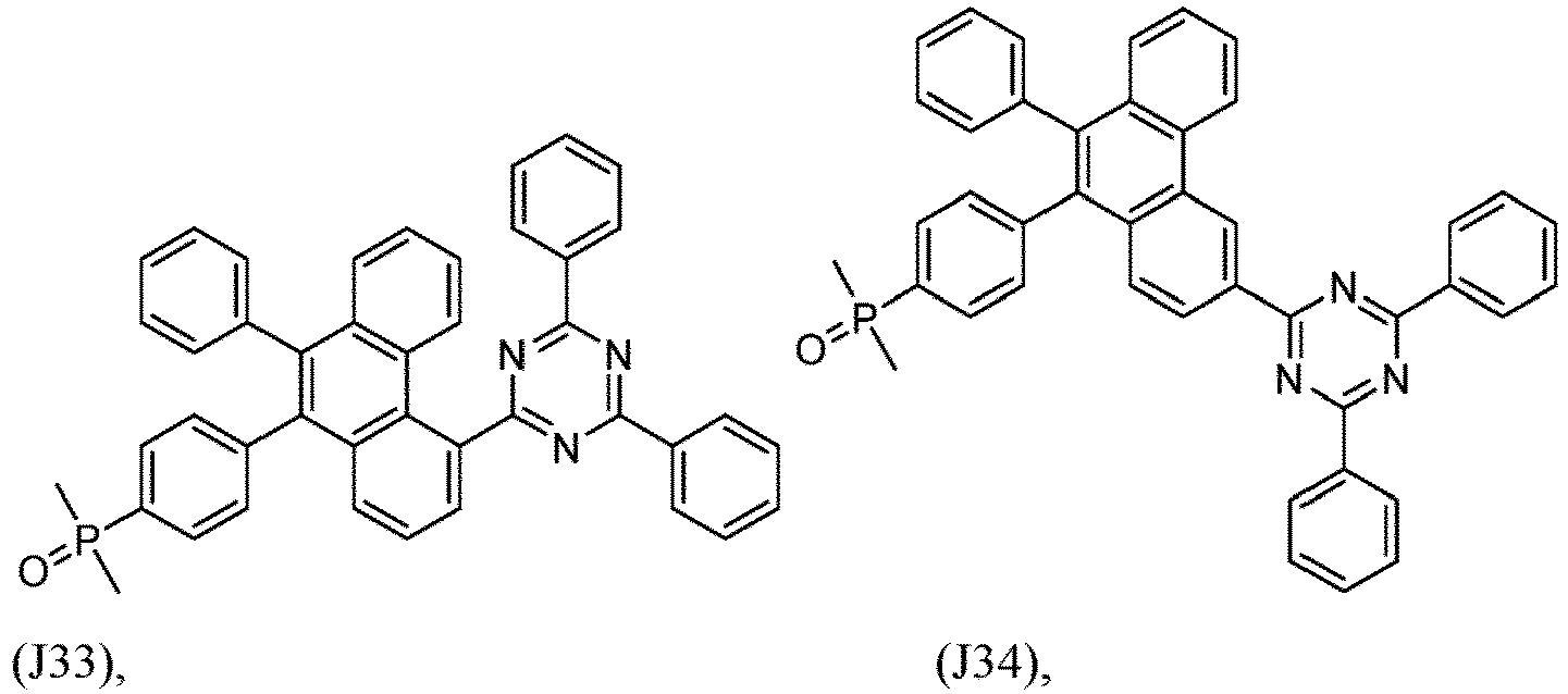
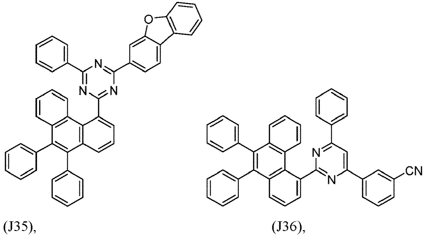
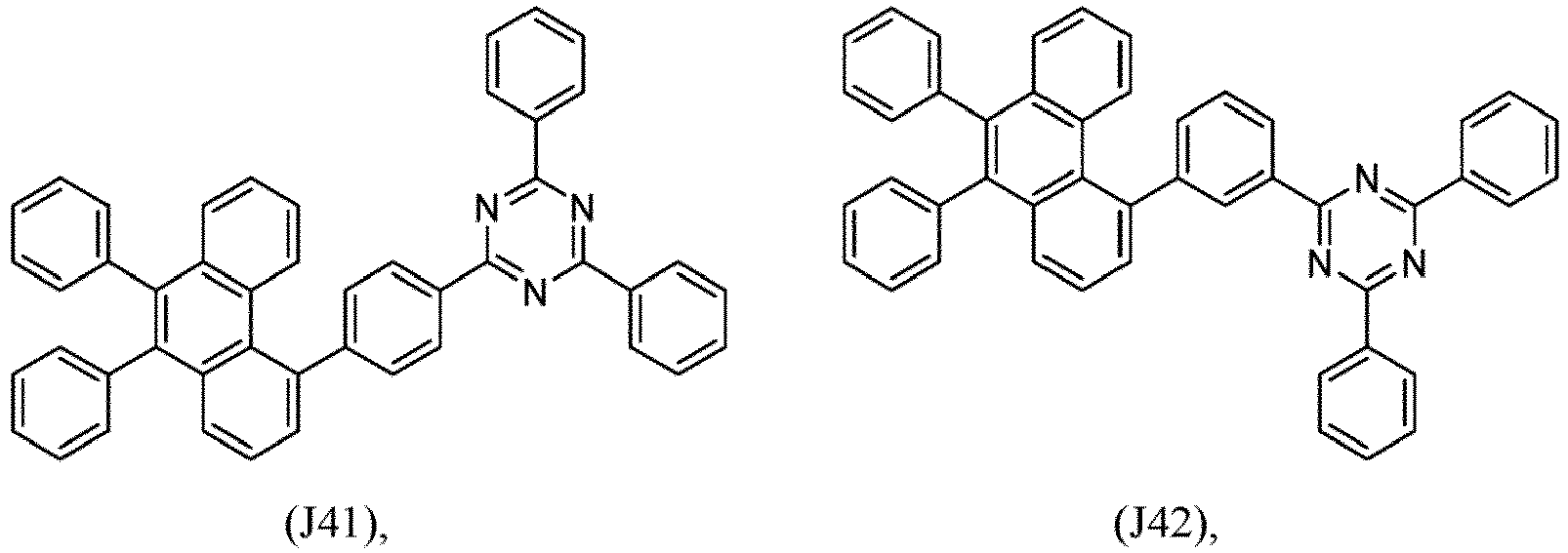
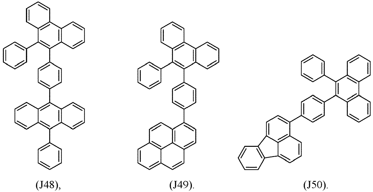
- Verbindung der Formel 1 gemäß einem der Ansprüche 1 bis 14, wobei die Verbindung der Formel 1 ausgewählt ist aus J1 bis J53:


- Organische Halbleiterschicht, umfassend wenigstens eine Verbindung 1 gemäß einem der vorstehenden Ansprüche 1 bis 15.
- Organische Halbleiterschicht gemäß Anspruch 16, wobei die organische Halbleiterschicht ferner ein Metall, ein Metallsalz oder einen organischen Metallkomplex umfasst, vorzugsweise einen organischen einwertigen oder zweiwertigen Metallkomplex, bevorzugter LiQ oder Alkaliborat.
- Organische elektronische Vorrichtung, umfassend eine Anodenschicht, eine Kathodenschicht und wenigstens eine organische Halbleiterschicht gemäß Anspruch 16 oder 17. wobei die wenigstens eine organische Halbleiterschicht eine Verbindung der Formel 1 gemäß einem der vorstehenden Ansprüche 1 bis 13 umfasst.
- Organische elektronische Vorrichtung gemäß Anspruch 18, ferner umfassend wenigstens eine Emissionsschicht, wobei die organische Halbleiterschicht zwischen der wenigstens einen Emissionsschicht und der Kathodenschicht angeordnet ist.
- Organische elektronische Vorrichtung gemäß Anspruch 18 oder 19, wobei die organische elektronische Vorrichtung eine lichtemittierende Vorrichtung, ein Dünnschichttransistor, eine Batterie, eine Anzeigevorrichtung oder eine Photovoltaikzelle, vorzugsweise eine lichtemittierende Vorrichtung, ist.
Priority Applications (7)
| Application Number | Priority Date | Filing Date | Title |
|---|---|---|---|
| EP18184297.2A EP3598515B1 (de) | 2018-07-18 | 2018-07-18 | Verbindung und organische halbleitende schicht, organische elektronische vorrichtung, anzeigevorrichtung und beleuchtungsvorrichtung damit |
| TW108123793A TWI886100B (zh) | 2018-07-18 | 2019-07-05 | 化合物及含此之有機半導體層、有機電子元件、顯示裝置及照明裝置 |
| PCT/EP2019/069132 WO2020016233A1 (en) | 2018-07-18 | 2019-07-16 | Compound and organic semiconducting layer, organic electronic device, display device and lighting device comprising the same |
| US17/259,762 US12108664B2 (en) | 2018-07-18 | 2019-07-16 | Compound and organic semiconducting layer, organic electronic device, display device and lighting device comprising the same |
| EP19739616.1A EP3824500A1 (de) | 2018-07-18 | 2019-07-16 | Verbindung und organische halbleitende schicht, organische elektronische vorrichtung, anzeigevorrichtung und beleuchtungsvorrichtung damit |
| CN201980047472.3A CN112514097A (zh) | 2018-07-18 | 2019-07-16 | 化合物以及包含所述化合物的有机半导体层、有机电子器件、显示装置和照明装置 |
| KR1020217004507A KR102893669B1 (ko) | 2018-07-18 | 2019-07-16 | 화합물 및 상기 화합물을 포함하는 유기 반도체 층, 유기 전자 장치, 디스플레이 장치 및 발광 장치 |
Applications Claiming Priority (1)
| Application Number | Priority Date | Filing Date | Title |
|---|---|---|---|
| EP18184297.2A EP3598515B1 (de) | 2018-07-18 | 2018-07-18 | Verbindung und organische halbleitende schicht, organische elektronische vorrichtung, anzeigevorrichtung und beleuchtungsvorrichtung damit |
Publications (2)
| Publication Number | Publication Date |
|---|---|
| EP3598515A1 EP3598515A1 (de) | 2020-01-22 |
| EP3598515B1 true EP3598515B1 (de) | 2024-09-04 |
Family
ID=62986012
Family Applications (2)
| Application Number | Title | Priority Date | Filing Date |
|---|---|---|---|
| EP18184297.2A Active EP3598515B1 (de) | 2018-07-18 | 2018-07-18 | Verbindung und organische halbleitende schicht, organische elektronische vorrichtung, anzeigevorrichtung und beleuchtungsvorrichtung damit |
| EP19739616.1A Pending EP3824500A1 (de) | 2018-07-18 | 2019-07-16 | Verbindung und organische halbleitende schicht, organische elektronische vorrichtung, anzeigevorrichtung und beleuchtungsvorrichtung damit |
Family Applications After (1)
| Application Number | Title | Priority Date | Filing Date |
|---|---|---|---|
| EP19739616.1A Pending EP3824500A1 (de) | 2018-07-18 | 2019-07-16 | Verbindung und organische halbleitende schicht, organische elektronische vorrichtung, anzeigevorrichtung und beleuchtungsvorrichtung damit |
Country Status (6)
| Country | Link |
|---|---|
| US (1) | US12108664B2 (de) |
| EP (2) | EP3598515B1 (de) |
| KR (1) | KR102893669B1 (de) |
| CN (1) | CN112514097A (de) |
| TW (1) | TWI886100B (de) |
| WO (1) | WO2020016233A1 (de) |
Families Citing this family (10)
| Publication number | Priority date | Publication date | Assignee | Title |
|---|---|---|---|---|
| EP3667753B1 (de) * | 2018-12-14 | 2025-04-23 | Novaled GmbH | Organische lichtemittierende vorrichtung und eine verbindung zur verwendung darin |
| CN112851645B (zh) * | 2019-11-28 | 2023-06-23 | 南京高光半导体材料有限公司 | 一种基于三嗪环结构的有机电致发光材料及有机电致发光器件 |
| CN111187228B (zh) * | 2020-02-04 | 2023-08-01 | 上海传勤新材料有限公司 | 一种基于菲和苯甲腈的有机电子材料及其应用 |
| JP7716865B2 (ja) * | 2020-03-31 | 2025-08-01 | 東ソー株式会社 | 環状アジン化合物、その製造法、およびその用途 |
| CN111740020B (zh) * | 2020-06-07 | 2023-05-26 | 上海传勤新材料有限公司 | 一种高效长寿命的蓝光器件 |
| CN114835686B (zh) * | 2021-02-02 | 2024-10-11 | 江苏三月科技股份有限公司 | 一种含有菲与三嗪结构的化合物及其应用 |
| EP4060756A1 (de) * | 2021-03-19 | 2022-09-21 | Idemitsu Kosan Co., Ltd. | Organische elektrolumineszvorrichtung mit einer azinverbindung und einem seltenerdmetall, seltenerdmetallverbindung und/oder seltenerdmetallkomplex und eine elektronische ausrüstung mit der organischen elektrolumineszenzvorrichtung |
| CN114349742A (zh) * | 2021-11-18 | 2022-04-15 | 上海和辉光电股份有限公司 | 一种含有菲的有机电致发光化合物及其应用 |
| CN114702489A (zh) * | 2022-04-07 | 2022-07-05 | 上海传勤新材料有限公司 | 一种含有菲和邻菲罗啉的有机电子材料及其应用 |
| WO2024005118A1 (ja) * | 2022-07-01 | 2024-01-04 | 東ソー株式会社 | 有機電界発光素子 |
Family Cites Families (26)
| Publication number | Priority date | Publication date | Assignee | Title |
|---|---|---|---|---|
| US6800380B2 (en) | 1998-06-23 | 2004-10-05 | Nessdisplay Co., Ltd. | Organometallic luminescent materials and organic electroluminescent device containing same |
| US6140763A (en) | 1998-07-28 | 2000-10-31 | Eastman Kodak Company | Interfacial electron-injecting layer formed from a doped cathode for organic light-emitting structure |
| KR100329571B1 (ko) | 2000-03-27 | 2002-03-23 | 김순택 | 유기 전자 발광소자 |
| JP3945123B2 (ja) | 2000-04-10 | 2007-07-18 | 三菱化学株式会社 | 有機電界発光素子 |
| ATE346127T1 (de) * | 2001-04-26 | 2006-12-15 | Fuji Photo Film Co Ltd | Aromatische verbindungen mit kondensierten ringen,materialien für lichtemittierende geräte und lichtemittierende geräte in denen solche verwendet werden |
| KR100669717B1 (ko) * | 2004-07-29 | 2007-01-16 | 삼성에스디아이 주식회사 | 유기 전계 발광 소자 |
| JP2008195623A (ja) | 2007-02-08 | 2008-08-28 | Chemiprokasei Kaisha Ltd | 新規な複素環含有ヒドロキシフェニル金属誘導体およびそれを用いた電子注入材料、電子輸送材料および有機エレクトロルミネッセンス素子 |
| DE102008008953B4 (de) | 2008-02-13 | 2019-05-09 | Merck Patent Gmbh | Neue Materialien für organische Elektrolumineszenzvorrichtungen |
| WO2010074087A1 (ja) * | 2008-12-26 | 2010-07-01 | 出光興産株式会社 | 有機エレクトロルミネッセンス素子用材料及び有機エレクトロルミネッセンス素子 |
| DE102009053644B4 (de) * | 2009-11-17 | 2019-07-04 | Merck Patent Gmbh | Materialien für organische Elektrolumineszenzvorrichtungen |
| JP4617393B1 (ja) * | 2010-01-15 | 2011-01-26 | 富士フイルム株式会社 | 有機電界発光素子 |
| JP5872930B2 (ja) * | 2011-03-31 | 2016-03-01 | ユー・ディー・シー アイルランド リミテッド | 有機電界発光素子及び電荷輸送材料 |
| TWI558711B (zh) | 2011-11-30 | 2016-11-21 | 諾瓦發光二極體有限公司 | 有機電子裝置 |
| KR102026369B1 (ko) | 2011-11-30 | 2019-09-27 | 노발레드 게엠베하 | 디스플레이 |
| KR102476782B1 (ko) | 2011-11-30 | 2022-12-09 | 노발레드 게엠베하 | 유기 전자 소자 |
| TWI597285B (zh) * | 2012-11-06 | 2017-09-01 | Udc愛爾蘭責任有限公司 | 用於電子應用之以啡噁矽(phenoxasiline)為基之化合物 |
| KR20150075169A (ko) * | 2013-12-24 | 2015-07-03 | 희성소재 (주) | 함질소 다환 화합물 및 이를 이용한 유기발광소자 |
| KR20150076503A (ko) * | 2013-12-27 | 2015-07-07 | 희성소재 (주) | 피리미딘계 화합물 및 이를 이용한 유기발광소자 |
| KR102295197B1 (ko) * | 2014-12-30 | 2021-09-01 | 엘티소재주식회사 | 화합물 및 이를 이용한 유기발광소자 |
| KR102321381B1 (ko) | 2015-02-23 | 2021-11-04 | 삼성디스플레이 주식회사 | 유기 발광 소자 |
| KR102662806B1 (ko) * | 2015-08-28 | 2024-05-02 | 메르크 파텐트 게엠베하 | 전자 소자용 화합물 |
| KR102688750B1 (ko) | 2015-09-03 | 2024-07-29 | 루미리즈 홀딩 비.브이. | Led 디바이스 제조 방법 |
| JP2017154988A (ja) * | 2016-02-29 | 2017-09-07 | 国立大学法人東京工業大学 | π共役化合物およびその製造方法 |
| EP3312895B1 (de) * | 2016-10-24 | 2021-07-28 | Novaled GmbH | Organisches halbleitermaterial mit einem elektrischen n-dotierstoff sowie elektronentransportmatrix und elektronische vorrichtung mit dem halbleitermaterial |
| KR101959514B1 (ko) * | 2017-02-21 | 2019-03-18 | 주식회사 엘지화학 | 신규한 헤테로 고리 화합물 및 이를 이용한 유기 발광 소자 |
| CN108409666A (zh) * | 2018-02-07 | 2018-08-17 | 瑞声科技(南京)有限公司 | 一种有机发光材料及其器件应用 |
-
2018
- 2018-07-18 EP EP18184297.2A patent/EP3598515B1/de active Active
-
2019
- 2019-07-05 TW TW108123793A patent/TWI886100B/zh active
- 2019-07-16 CN CN201980047472.3A patent/CN112514097A/zh active Pending
- 2019-07-16 EP EP19739616.1A patent/EP3824500A1/de active Pending
- 2019-07-16 WO PCT/EP2019/069132 patent/WO2020016233A1/en not_active Ceased
- 2019-07-16 KR KR1020217004507A patent/KR102893669B1/ko active Active
- 2019-07-16 US US17/259,762 patent/US12108664B2/en active Active
Also Published As
| Publication number | Publication date |
|---|---|
| KR102893669B1 (ko) | 2025-12-01 |
| EP3824500A1 (de) | 2021-05-26 |
| CN112514097A (zh) | 2021-03-16 |
| EP3598515A1 (de) | 2020-01-22 |
| TW202016256A (zh) | 2020-05-01 |
| US12108664B2 (en) | 2024-10-01 |
| US20210367157A1 (en) | 2021-11-25 |
| KR20210034619A (ko) | 2021-03-30 |
| TWI886100B (zh) | 2025-06-11 |
| WO2020016233A1 (en) | 2020-01-23 |
Similar Documents
| Publication | Publication Date | Title |
|---|---|---|
| EP3598515B1 (de) | Verbindung und organische halbleitende schicht, organische elektronische vorrichtung, anzeigevorrichtung und beleuchtungsvorrichtung damit | |
| EP3689867B1 (de) | Zusammensetzung, organische halbleiterschicht und elektronische vorrichtung | |
| EP4035217B1 (de) | Erste und zweite organische halbleiterschicht und organische elektronische vorrichtung, dieselbe umfassend | |
| EP3502106B1 (de) | Mit voluminösen gruppen substituierte triazinverbindungen | |
| EP3470398B1 (de) | Organische elektronische vorrichtung mit einer organischen halbleiterschicht | |
| EP3790875B1 (de) | N-heteroarylen-verbindungen mit niedrigen lumo-energien | |
| EP3470412B1 (de) | Organische elektronische vorrichtung mit einer organischen halbleiterschicht | |
| EP3835295A1 (de) | Acridin-verbindung und organische halbleitende schicht, organische elektronische vorrichtung und anzeigevorrichtung damit | |
| EP3589617B1 (de) | Acridinverbindung zur verwendung in einer elektronischen vorrichtung und elektronische vorrichtung | |
| EP3503240B1 (de) | Organische halbleiterschicht | |
| EP3990450B1 (de) | Mit voluminösen gruppen substituierte triazinverbindungen | |
| EP3483157B1 (de) | Verbindungen mit triazingruppe, fluorengruppe und heterofluorengruppe | |
| EP3798213B1 (de) | Organische halbleiterschicht, organische elektronische vorrichtung damit und verbindungen dafür | |
| KR102639012B1 (ko) | 트리아진기, 플루오렌기 및 아릴기를 포함하는 화합물 | |
| EP3527557A1 (de) | N-heteroarylen-verbindungen | |
| EP3733649A1 (de) | Hetero-fluorene derivate und deren verwendung in elektronischen einrichtungen | |
| KR102685005B1 (ko) | 트리아진기, 플루오렌기 및 아릴기를 포함하는 화합물 | |
| EP3643720B1 (de) | Organische verbindungen, organische halbleiterschicht und organische elektronische vorrichtung |
Legal Events
| Date | Code | Title | Description |
|---|---|---|---|
| PUAI | Public reference made under article 153(3) epc to a published international application that has entered the european phase |
Free format text: ORIGINAL CODE: 0009012 |
|
| STAA | Information on the status of an ep patent application or granted ep patent |
Free format text: STATUS: THE APPLICATION HAS BEEN PUBLISHED |
|
| AK | Designated contracting states |
Kind code of ref document: A1 Designated state(s): AL AT BE BG CH CY CZ DE DK EE ES FI FR GB GR HR HU IE IS IT LI LT LU LV MC MK MT NL NO PL PT RO RS SE SI SK SM TR |
|
| AX | Request for extension of the european patent |
Extension state: BA ME |
|
| RAP1 | Party data changed (applicant data changed or rights of an application transferred) |
Owner name: NOVALED GMBH |
|
| STAA | Information on the status of an ep patent application or granted ep patent |
Free format text: STATUS: REQUEST FOR EXAMINATION WAS MADE |
|
| 17P | Request for examination filed |
Effective date: 20200720 |
|
| RBV | Designated contracting states (corrected) |
Designated state(s): AL AT BE BG CH CY CZ DE DK EE ES FI FR GB GR HR HU IE IS IT LI LT LU LV MC MK MT NL NO PL PT RO RS SE SI SK SM TR |
|
| STAA | Information on the status of an ep patent application or granted ep patent |
Free format text: STATUS: EXAMINATION IS IN PROGRESS |
|
| 17Q | First examination report despatched |
Effective date: 20230210 |
|
| REG | Reference to a national code |
Ref country code: DE Ipc: C07D0221180000 Ref country code: DE Ref legal event code: R079 Ref document number: 602018073873 Country of ref document: DE Free format text: PREVIOUS MAIN CLASS: H01L0051300000 Ipc: C07D0221180000 |
|
| GRAP | Despatch of communication of intention to grant a patent |
Free format text: ORIGINAL CODE: EPIDOSNIGR1 |
|
| STAA | Information on the status of an ep patent application or granted ep patent |
Free format text: STATUS: GRANT OF PATENT IS INTENDED |
|
| RIC1 | Information provided on ipc code assigned before grant |
Ipc: H10K 85/60 20230101ALI20240315BHEP Ipc: C07D 401/10 20060101ALI20240315BHEP Ipc: C07D 409/04 20060101ALI20240315BHEP Ipc: C07F 9/6521 20060101ALI20240315BHEP Ipc: C07F 9/53 20060101ALI20240315BHEP Ipc: C07D 405/04 20060101ALI20240315BHEP Ipc: C07D 239/70 20060101ALI20240315BHEP Ipc: C07D 403/10 20060101ALI20240315BHEP Ipc: C07D 251/24 20060101ALI20240315BHEP Ipc: C07D 239/26 20060101ALI20240315BHEP Ipc: C07D 221/18 20060101AFI20240315BHEP |
|
| INTG | Intention to grant announced |
Effective date: 20240408 |
|
| GRAS | Grant fee paid |
Free format text: ORIGINAL CODE: EPIDOSNIGR3 |
|
| GRAA | (expected) grant |
Free format text: ORIGINAL CODE: 0009210 |
|
| STAA | Information on the status of an ep patent application or granted ep patent |
Free format text: STATUS: THE PATENT HAS BEEN GRANTED |
|
| P01 | Opt-out of the competence of the unified patent court (upc) registered |
Free format text: CASE NUMBER: APP_39535/2024 Effective date: 20240703 |
|
| AK | Designated contracting states |
Kind code of ref document: B1 Designated state(s): AL AT BE BG CH CY CZ DE DK EE ES FI FR GB GR HR HU IE IS IT LI LT LU LV MC MK MT NL NO PL PT RO RS SE SI SK SM TR |
|
| REG | Reference to a national code |
Ref country code: GB Ref legal event code: FG4D |
|
| REG | Reference to a national code |
Ref country code: CH Ref legal event code: EP |
|
| REG | Reference to a national code |
Ref country code: IE Ref legal event code: FG4D |
|
| REG | Reference to a national code |
Ref country code: DE Ref legal event code: R096 Ref document number: 602018073873 Country of ref document: DE |
|
| REG | Reference to a national code |
Ref country code: LT Ref legal event code: MG9D |
|
| REG | Reference to a national code |
Ref country code: NL Ref legal event code: MP Effective date: 20240904 |
|
| PG25 | Lapsed in a contracting state [announced via postgrant information from national office to epo] |
Ref country code: NO Free format text: LAPSE BECAUSE OF FAILURE TO SUBMIT A TRANSLATION OF THE DESCRIPTION OR TO PAY THE FEE WITHIN THE PRESCRIBED TIME-LIMIT Effective date: 20241204 |
|
| PG25 | Lapsed in a contracting state [announced via postgrant information from national office to epo] |
Ref country code: FI Free format text: LAPSE BECAUSE OF FAILURE TO SUBMIT A TRANSLATION OF THE DESCRIPTION OR TO PAY THE FEE WITHIN THE PRESCRIBED TIME-LIMIT Effective date: 20240904 Ref country code: GR Free format text: LAPSE BECAUSE OF FAILURE TO SUBMIT A TRANSLATION OF THE DESCRIPTION OR TO PAY THE FEE WITHIN THE PRESCRIBED TIME-LIMIT Effective date: 20241205 Ref country code: PL Free format text: LAPSE BECAUSE OF FAILURE TO SUBMIT A TRANSLATION OF THE DESCRIPTION OR TO PAY THE FEE WITHIN THE PRESCRIBED TIME-LIMIT Effective date: 20240904 |
|
| PG25 | Lapsed in a contracting state [announced via postgrant information from national office to epo] |
Ref country code: BG Free format text: LAPSE BECAUSE OF FAILURE TO SUBMIT A TRANSLATION OF THE DESCRIPTION OR TO PAY THE FEE WITHIN THE PRESCRIBED TIME-LIMIT Effective date: 20240904 |
|
| PG25 | Lapsed in a contracting state [announced via postgrant information from national office to epo] |
Ref country code: LV Free format text: LAPSE BECAUSE OF FAILURE TO SUBMIT A TRANSLATION OF THE DESCRIPTION OR TO PAY THE FEE WITHIN THE PRESCRIBED TIME-LIMIT Effective date: 20240904 |
|
| PG25 | Lapsed in a contracting state [announced via postgrant information from national office to epo] |
Ref country code: HR Free format text: LAPSE BECAUSE OF FAILURE TO SUBMIT A TRANSLATION OF THE DESCRIPTION OR TO PAY THE FEE WITHIN THE PRESCRIBED TIME-LIMIT Effective date: 20240904 |
|
| PG25 | Lapsed in a contracting state [announced via postgrant information from national office to epo] |
Ref country code: ES Free format text: LAPSE BECAUSE OF FAILURE TO SUBMIT A TRANSLATION OF THE DESCRIPTION OR TO PAY THE FEE WITHIN THE PRESCRIBED TIME-LIMIT Effective date: 20240904 Ref country code: RS Free format text: LAPSE BECAUSE OF FAILURE TO SUBMIT A TRANSLATION OF THE DESCRIPTION OR TO PAY THE FEE WITHIN THE PRESCRIBED TIME-LIMIT Effective date: 20241204 |
|
| PG25 | Lapsed in a contracting state [announced via postgrant information from national office to epo] |
Ref country code: RS Free format text: LAPSE BECAUSE OF FAILURE TO SUBMIT A TRANSLATION OF THE DESCRIPTION OR TO PAY THE FEE WITHIN THE PRESCRIBED TIME-LIMIT Effective date: 20241204 Ref country code: PL Free format text: LAPSE BECAUSE OF FAILURE TO SUBMIT A TRANSLATION OF THE DESCRIPTION OR TO PAY THE FEE WITHIN THE PRESCRIBED TIME-LIMIT Effective date: 20240904 Ref country code: NO Free format text: LAPSE BECAUSE OF FAILURE TO SUBMIT A TRANSLATION OF THE DESCRIPTION OR TO PAY THE FEE WITHIN THE PRESCRIBED TIME-LIMIT Effective date: 20241204 Ref country code: LV Free format text: LAPSE BECAUSE OF FAILURE TO SUBMIT A TRANSLATION OF THE DESCRIPTION OR TO PAY THE FEE WITHIN THE PRESCRIBED TIME-LIMIT Effective date: 20240904 Ref country code: HR Free format text: LAPSE BECAUSE OF FAILURE TO SUBMIT A TRANSLATION OF THE DESCRIPTION OR TO PAY THE FEE WITHIN THE PRESCRIBED TIME-LIMIT Effective date: 20240904 Ref country code: GR Free format text: LAPSE BECAUSE OF FAILURE TO SUBMIT A TRANSLATION OF THE DESCRIPTION OR TO PAY THE FEE WITHIN THE PRESCRIBED TIME-LIMIT Effective date: 20241205 Ref country code: FI Free format text: LAPSE BECAUSE OF FAILURE TO SUBMIT A TRANSLATION OF THE DESCRIPTION OR TO PAY THE FEE WITHIN THE PRESCRIBED TIME-LIMIT Effective date: 20240904 Ref country code: ES Free format text: LAPSE BECAUSE OF FAILURE TO SUBMIT A TRANSLATION OF THE DESCRIPTION OR TO PAY THE FEE WITHIN THE PRESCRIBED TIME-LIMIT Effective date: 20240904 Ref country code: BG Free format text: LAPSE BECAUSE OF FAILURE TO SUBMIT A TRANSLATION OF THE DESCRIPTION OR TO PAY THE FEE WITHIN THE PRESCRIBED TIME-LIMIT Effective date: 20240904 |
|
| REG | Reference to a national code |
Ref country code: AT Ref legal event code: MK05 Ref document number: 1720281 Country of ref document: AT Kind code of ref document: T Effective date: 20240904 |
|
| PG25 | Lapsed in a contracting state [announced via postgrant information from national office to epo] |
Ref country code: NL Free format text: LAPSE BECAUSE OF FAILURE TO SUBMIT A TRANSLATION OF THE DESCRIPTION OR TO PAY THE FEE WITHIN THE PRESCRIBED TIME-LIMIT Effective date: 20240904 |
|
| PG25 | Lapsed in a contracting state [announced via postgrant information from national office to epo] |
Ref country code: IS Free format text: LAPSE BECAUSE OF FAILURE TO SUBMIT A TRANSLATION OF THE DESCRIPTION OR TO PAY THE FEE WITHIN THE PRESCRIBED TIME-LIMIT Effective date: 20250104 Ref country code: PT Free format text: LAPSE BECAUSE OF FAILURE TO SUBMIT A TRANSLATION OF THE DESCRIPTION OR TO PAY THE FEE WITHIN THE PRESCRIBED TIME-LIMIT Effective date: 20250106 |
|
| PG25 | Lapsed in a contracting state [announced via postgrant information from national office to epo] |
Ref country code: SM Free format text: LAPSE BECAUSE OF FAILURE TO SUBMIT A TRANSLATION OF THE DESCRIPTION OR TO PAY THE FEE WITHIN THE PRESCRIBED TIME-LIMIT Effective date: 20240904 Ref country code: RO Free format text: LAPSE BECAUSE OF FAILURE TO SUBMIT A TRANSLATION OF THE DESCRIPTION OR TO PAY THE FEE WITHIN THE PRESCRIBED TIME-LIMIT Effective date: 20240904 |
|
| PG25 | Lapsed in a contracting state [announced via postgrant information from national office to epo] |
Ref country code: EE Free format text: LAPSE BECAUSE OF FAILURE TO SUBMIT A TRANSLATION OF THE DESCRIPTION OR TO PAY THE FEE WITHIN THE PRESCRIBED TIME-LIMIT Effective date: 20240904 Ref country code: AT Free format text: LAPSE BECAUSE OF FAILURE TO SUBMIT A TRANSLATION OF THE DESCRIPTION OR TO PAY THE FEE WITHIN THE PRESCRIBED TIME-LIMIT Effective date: 20240904 |
|
| PG25 | Lapsed in a contracting state [announced via postgrant information from national office to epo] |
Ref country code: CZ Free format text: LAPSE BECAUSE OF FAILURE TO SUBMIT A TRANSLATION OF THE DESCRIPTION OR TO PAY THE FEE WITHIN THE PRESCRIBED TIME-LIMIT Effective date: 20240904 |
|
| PG25 | Lapsed in a contracting state [announced via postgrant information from national office to epo] |
Ref country code: IT Free format text: LAPSE BECAUSE OF FAILURE TO SUBMIT A TRANSLATION OF THE DESCRIPTION OR TO PAY THE FEE WITHIN THE PRESCRIBED TIME-LIMIT Effective date: 20240904 Ref country code: SK Free format text: LAPSE BECAUSE OF FAILURE TO SUBMIT A TRANSLATION OF THE DESCRIPTION OR TO PAY THE FEE WITHIN THE PRESCRIBED TIME-LIMIT Effective date: 20240904 |
|
| REG | Reference to a national code |
Ref country code: DE Ref legal event code: R097 Ref document number: 602018073873 Country of ref document: DE |
|
| PG25 | Lapsed in a contracting state [announced via postgrant information from national office to epo] |
Ref country code: DK Free format text: LAPSE BECAUSE OF FAILURE TO SUBMIT A TRANSLATION OF THE DESCRIPTION OR TO PAY THE FEE WITHIN THE PRESCRIBED TIME-LIMIT Effective date: 20240904 |
|
| PLBE | No opposition filed within time limit |
Free format text: ORIGINAL CODE: 0009261 |
|
| STAA | Information on the status of an ep patent application or granted ep patent |
Free format text: STATUS: NO OPPOSITION FILED WITHIN TIME LIMIT |
|
| 26N | No opposition filed |
Effective date: 20250605 |
|
| PG25 | Lapsed in a contracting state [announced via postgrant information from national office to epo] |
Ref country code: SE Free format text: LAPSE BECAUSE OF FAILURE TO SUBMIT A TRANSLATION OF THE DESCRIPTION OR TO PAY THE FEE WITHIN THE PRESCRIBED TIME-LIMIT Effective date: 20240904 |
|
| PGFP | Annual fee paid to national office [announced via postgrant information from national office to epo] |
Ref country code: DE Payment date: 20250528 Year of fee payment: 8 |