EP3580702B1 - Integration von schaltungselementen in eine gestapelte quanten-computing-vorrichtung - Google Patents
Integration von schaltungselementen in eine gestapelte quanten-computing-vorrichtung Download PDFInfo
- Publication number
- EP3580702B1 EP3580702B1 EP17825709.3A EP17825709A EP3580702B1 EP 3580702 B1 EP3580702 B1 EP 3580702B1 EP 17825709 A EP17825709 A EP 17825709A EP 3580702 B1 EP3580702 B1 EP 3580702B1
- Authority
- EP
- European Patent Office
- Prior art keywords
- chip
- qubit
- layer
- superconductor
- dielectric
- Prior art date
- Legal status (The legal status is an assumption and is not a legal conclusion. Google has not performed a legal analysis and makes no representation as to the accuracy of the status listed.)
- Active
Links
Images


Classifications
-
- G—PHYSICS
- G06—COMPUTING OR CALCULATING; COUNTING
- G06N—COMPUTING ARRANGEMENTS BASED ON SPECIFIC COMPUTATIONAL MODELS
- G06N10/00—Quantum computing, i.e. information processing based on quantum-mechanical phenomena
- G06N10/40—Physical realisations or architectures of quantum processors or components for manipulating qubits, e.g. qubit coupling or qubit control
-
- G—PHYSICS
- G06—COMPUTING OR CALCULATING; COUNTING
- G06N—COMPUTING ARRANGEMENTS BASED ON SPECIFIC COMPUTATIONAL MODELS
- G06N10/00—Quantum computing, i.e. information processing based on quantum-mechanical phenomena
-
- H—ELECTRICITY
- H10—SEMICONDUCTOR DEVICES; ELECTRIC SOLID-STATE DEVICES NOT OTHERWISE PROVIDED FOR
- H10N—ELECTRIC SOLID-STATE DEVICES NOT OTHERWISE PROVIDED FOR
- H10N60/00—Superconducting devices
- H10N60/20—Permanent superconducting devices
-
- H—ELECTRICITY
- H10—SEMICONDUCTOR DEVICES; ELECTRIC SOLID-STATE DEVICES NOT OTHERWISE PROVIDED FOR
- H10N—ELECTRIC SOLID-STATE DEVICES NOT OTHERWISE PROVIDED FOR
- H10N69/00—Integrated devices, or assemblies of multiple devices, comprising at least one superconducting element covered by group H10N60/00
-
- H—ELECTRICITY
- H10—SEMICONDUCTOR DEVICES; ELECTRIC SOLID-STATE DEVICES NOT OTHERWISE PROVIDED FOR
- H10W—GENERIC PACKAGES, INTERCONNECTIONS, CONNECTORS OR OTHER CONSTRUCTIONAL DETAILS OF DEVICES COVERED BY CLASS H10
- H10W20/00—Interconnections in chips, wafers or substrates
- H10W20/40—Interconnections external to wafers or substrates, e.g. back-end-of-line [BEOL] metallisations or vias connecting to gate electrodes
- H10W20/41—Interconnections external to wafers or substrates, e.g. back-end-of-line [BEOL] metallisations or vias connecting to gate electrodes characterised by their conductive parts
- H10W20/423—Shielding layers
-
- H—ELECTRICITY
- H10—SEMICONDUCTOR DEVICES; ELECTRIC SOLID-STATE DEVICES NOT OTHERWISE PROVIDED FOR
- H10W—GENERIC PACKAGES, INTERCONNECTIONS, CONNECTORS OR OTHER CONSTRUCTIONAL DETAILS OF DEVICES COVERED BY CLASS H10
- H10W42/00—Arrangements for protection of devices
- H10W42/20—Arrangements for protection of devices protecting against electromagnetic or particle radiation, e.g. light, X-rays, gamma-rays or electrons
-
- H—ELECTRICITY
- H10—SEMICONDUCTOR DEVICES; ELECTRIC SOLID-STATE DEVICES NOT OTHERWISE PROVIDED FOR
- H10W—GENERIC PACKAGES, INTERCONNECTIONS, CONNECTORS OR OTHER CONSTRUCTIONAL DETAILS OF DEVICES COVERED BY CLASS H10
- H10W72/00—Interconnections or connectors in packages
- H10W72/20—Bump connectors, e.g. solder bumps or copper pillars; Dummy bumps; Thermal bumps
-
- H—ELECTRICITY
- H10—SEMICONDUCTOR DEVICES; ELECTRIC SOLID-STATE DEVICES NOT OTHERWISE PROVIDED FOR
- H10W—GENERIC PACKAGES, INTERCONNECTIONS, CONNECTORS OR OTHER CONSTRUCTIONAL DETAILS OF DEVICES COVERED BY CLASS H10
- H10W90/00—Package configurations
-
- H—ELECTRICITY
- H10—SEMICONDUCTOR DEVICES; ELECTRIC SOLID-STATE DEVICES NOT OTHERWISE PROVIDED FOR
- H10W—GENERIC PACKAGES, INTERCONNECTIONS, CONNECTORS OR OTHER CONSTRUCTIONAL DETAILS OF DEVICES COVERED BY CLASS H10
- H10W72/00—Interconnections or connectors in packages
- H10W72/20—Bump connectors, e.g. solder bumps or copper pillars; Dummy bumps; Thermal bumps
- H10W72/251—Materials
- H10W72/252—Materials comprising solid metals or solid metalloids, e.g. PbSn, Ag or Cu
-
- H—ELECTRICITY
- H10—SEMICONDUCTOR DEVICES; ELECTRIC SOLID-STATE DEVICES NOT OTHERWISE PROVIDED FOR
- H10W—GENERIC PACKAGES, INTERCONNECTIONS, CONNECTORS OR OTHER CONSTRUCTIONAL DETAILS OF DEVICES COVERED BY CLASS H10
- H10W72/00—Interconnections or connectors in packages
- H10W72/20—Bump connectors, e.g. solder bumps or copper pillars; Dummy bumps; Thermal bumps
- H10W72/251—Materials
- H10W72/255—Materials of outermost layers of multilayered bumps, e.g. material of a coating
-
- H—ELECTRICITY
- H10—SEMICONDUCTOR DEVICES; ELECTRIC SOLID-STATE DEVICES NOT OTHERWISE PROVIDED FOR
- H10W—GENERIC PACKAGES, INTERCONNECTIONS, CONNECTORS OR OTHER CONSTRUCTIONAL DETAILS OF DEVICES COVERED BY CLASS H10
- H10W90/00—Package configurations
- H10W90/701—Package configurations characterised by the relative positions of pads or connectors relative to package parts
- H10W90/721—Package configurations characterised by the relative positions of pads or connectors relative to package parts of bump connectors
- H10W90/722—Package configurations characterised by the relative positions of pads or connectors relative to package parts of bump connectors between stacked chips
Definitions
- the present disclosure relates to integrating circuit elements in stacked quantum computing device.
- Quantum computing is a relatively new computing method that takes advantage of quantum effects, such as superposition of basis states and entanglement to perform certain computations more efficiently than a classical digital computer.
- quantum computing systems can manipulate information using qubits.
- a qubit can refer to a quantum device that enables the superposition of multiple states (e.g., data in both the "0" and "1" state) and/or to the superposition of data, itself, in the multiple states.
- the superposition of a "0" and “1” state in a quantum system may be represented, e.g., as ⁇
- the "0" and “1" states of a digital computer are analogous to the
- 2 represents the probability that a qubit is in
- 2 represents the probability that a qubit is in the
- the lossy materials and qubit control wiring may be formed on one or more chips within the stack that are separate from the chip containing the qubits.
- the chip containing the qubits By limiting the chip containing the qubits to high quality (low loss) materials, the qubits are substantially isolated from lossy material and qubit decoherence can be reduced.
- the qubit layout and wiring constraints may be relaxed.
- the qubit readout elements also may be moved to the same chip on which the wiring and lossy materials are formed.
- the control elements and wiring may be covered by a shielding layer and a dielectric layer.
- the qubit readout element may be provided without a dielectric layer or shielding layer.
- the devices and methods allow an increase in superconducting qubit density and/or qubit coupling through 3D integration.
- the fabrication steps for the superconducting qubits and the wiring/control elements are separated by putting the superconducting qubits on a first chip and the wiring/control elements on a second, separate chip.
- the devices and methods allow 3D integration to be achieved while reducing losses associated with processing methods and materials.
- the edges and corners of qubit readout resonator structures which are sensitive to processing are of higher quality, resulting in improved device quality factors.
- Quantum computing entails coherently processing quantum information stored in the quantum bits (qubits) of a quantum computer.
- Superconducting quantum computing is a promising implementation of quantum computing technology in which quantum computing circuit elements are formed, in part, from superconductor materials.
- Superconducting quantum computers are typically multilevel systems, in which only the first two levels are used as the computational basis.
- quantum circuit elements e.g., quantum computing circuit elements
- quantum computing circuit elements such as superconducting qubits
- the quantum computing circuit elements are operated with low energy loss and dissipation (e.g., the quantum computing circuit elements exhibit a high quality factor, Q). Low energy loss and dissipation may help to avoid, e.g., quantum decoherence.
- the superconducting qubits of the quantum processor are operatively coupled together in a controllable manner such that the quantum state of each superconducting qubit affects the corresponding quantum states of the other superconducting qubits to which it is coupled.
- the chosen architecture may limit the density and total number of superconducting qubits available for coupling, and thus limit the ability of the processor to perform complex problems requiring large numbers of superconducting qubits.
- the superconducting qubits may suffer energy loss and decoherence due to interactions with two level systems.
- the processor and associated circuit elements can be constructed using 3D integration. That is, instead of fabricating the quantum circuit elements of the processor within a single plane of a chip that extends along one and/or two dimensions (e.g., x- and/or y-directions), the quantum circuit elements can also be formed in multiple chips that are coupled together along a third dimension (e.g., z-direction).
- An approach for achieving 3D integration is to couple the chips using bump bonding, in which the chips are joined to one another by, e.g., superconductor bump bonds, to form a stacked device (e.g., a stacked quantum computing device).
- bump bonds may be used to electrically couple together components from different chips within the stack in addition to physical coupling of the chips.
- bump bonds solely may be used to provide physical coupling of different chips.
- the lossy materials and qubit control wiring may be formed on one or more chips within the stack that are separate from the chip or chips containing the qubits.
- the chip(s) containing the qubits By limiting the chip(s) containing the qubits to high quality (low loss) materials, the qubits are substantially isolated from lossy material and qubit decoherence can be reduced.
- the control wiring off the chip(s) containing the qubits the qubit layout and wiring constraints may be relaxed.
- the qubit readout elements also may be moved to the same chip on which the wiring and lossy materials are formed.
- readout resonators should maintain a modest level of coherence.
- a readout resonator although strongly coupled to the environment with a low coupling quality factor Qc, will damp the qubit if the intrinsic quality factor Qi is too low.
- the wiring should not be exposed.
- a first chip in the stacked quantum computing device includes superconducting qubits formed from high quality, coherent materials (low loss materials) and is bonded to a second chip that contains one or more wiring layers, as well as qubit control and qubit readout elements, integrated with lossy dielectrics.
- the qubit layout constraints on the first chip (as well as the wiring layout constraints on the second chip) can be relaxed.
- moving the lossy dielectric material to the second chip allows the qubits on the first chip to maintain high coherence (e.g., Q of about 1,000,000 or more).
- the qubit readout elements on the second chip may be formed without lossy dielectric on their surface, such that the readout elements maintain moderate coherence (e.g., Qi of about 200,000 or more).
- a shielding layer may be formed on the second chip to shield superconducting qubits on the first chip from the wiring on the second chip, to reduce crosstalk.
- the devices disclosed herein may be fabricated using processes that reduce residue and damage to the readout element, allowing the readout element to maintain moderate coherence.
- FIG. 1A is a schematic illustrating a side view of a stacked quantum computing device 100.
- the stacked quantum computing device 100 includes a first chip 102 and a second chip 104.
- the first chip 102 includes one or more quantum computing circuit elements (e.g., superconducting qubits) for use in performing data processing operations (e.g., quantum data processing operations).
- the first chip 102 includes a one-dimensional (1D) or two-dimensional (2D) array of superconducting qubits.
- the quantum computing circuit elements of the first chip 102 may be formed on and/or within a substrate.
- the substrate of the first chip may be formed from, e.g., a low loss dielectric suitable for quantum computing circuit elements, such as a silicon or sapphire wafer. Other materials may be used for the substrate instead.
- the second chip 104 includes additional quantum computing circuit elements such as, e.g., qubit control elements and qubit readout elements.
- the second chip 1 04 also may include wiring.
- qubit control elements include a qubit Z-control element for tuning a frequency of a qubit, and a qubit XY-control element for exciting a qubit.
- Each control element may be operable to couple (e.g., capacitively couple) to a qubit on the first chip 102.
- a qubit readout element may include, e.g., a resonator operable to couple (e.g., inductively couple) to a qubit of the first chip 102.
- the control elements, readout elements and wiring on the second chip 104 may be formed from superconductor material on a substrate of the second chip.
- the substrate of the second chip may be formed from, e.g., a low loss dielectric suitable for quantum computing circuit elements, such as a silicon or sapphire wafer. Other materials may be used for the substrate instead.
- the substrate of the first chip is a different substrate to the substrate of the second chip.
- the first chip 102 is aligned on top of the second chip 104 and connected physically to the second chip 104 using interconnects 106, such as bump bonds.
- the bump bonds 106 also provide an electrical connection between components of the first chip 102 and components of the second chip 104.
- the first chip 102 is connected to the second chip 104 through superconductor bump bonds 106 (e.g., bump bonds including indium). In some unclaimed implementations, a vacuum is maintained between the first chip 102 and the second chip 104.
- the bump bonds 106 may include superconductor material to avoid energy loss and decoherence of superconducting qubits that may be located, e.g., on the first chip 102.
- suitable superconductor material for use as a bump bond 106 includes, but is not limited to, indium, lead, rhenium, palladium, or niobium having a thin layer of non-superconductor material such as gold (e.g., between about 1 nm and about 100 nm).
- the thickness of the bump bonds 106 may be set so that the first chip 102 and the second chip 104 are spaced to achieve a desired capacitive or inductive coupling between circuit elements on the first chip 102 and on the second chip 104.
- a height of a gap 108 between the device surface of the first chip 102 and the structural element surface of the second chip 104 may be set to be between approximately 0.5 ⁇ m and approximately 100 ⁇ m (e.g., between approximately 10 ⁇ m and approximately 20 ⁇ m, between approximately 1 ⁇ m and 10 ⁇ m, between approximately 0.5 ⁇ m and approximately 20 ⁇ m, between approximately 0.5 ⁇ m and approximately 15 ⁇ m, between approximately 0.5 ⁇ m and approximately 10 ⁇ m, between approximately 0.5 ⁇ m and approximately 5 ⁇ m, or between approximately 0.5 ⁇ m and approximately 2.5 ⁇ m).
- FIG. 1B is a schematic illustrating a top view of circuit elements from a first chip as those circuit elements would be aligned with circuit elements from a second chip in an exemplary stacked quantum computation device (e.g., device 100).
- a first chip includes an array (e.g., a 2 x 2 array) of superconducting qubits 122.
- the qubits in the present unclaimed example are Xmon transmon qubits represented generally in the shape of a "plus" sign having four arms.
- Qubits 122 may include, but are not limited to, qubits such as flux qubits, transmon qubits, and gmon qubits.
- the second chip includes an array of qubit readout devices 124, in which each qubit readout device 124 is aligned with a corresponding superconducting qubit 122 from the first chip.
- Each qubit readout device 124 includes a resonator element 128 electrically coupled to a pad element 126.
- Each pad element 126 can be aligned over a center of a corresponding superconducting qubit 122 on the first chip.
- the region of the superconducting qubit 122 over which the pad element 126 is aligned may be referred to as a readout region 134 of the superconducting qubit 122.
- the pad element 126 is operable to capacitively couple to the readout region 134 of the qubit 122.
- the resonator element 128 may be laterally displaced with respect to the superconducting qubit 122 and electrically coupled to the pad element 128 through an elongated arm 130.
- the resonator element 128 may include, e.g., a transmission line resonator (e.g., a distributed element resonator or a lumped element resonator) such as a co-planar waveguide, where the length of the resonator determines the resonator frequency.
- a transmission line resonator e.g., a distributed element resonator or a lumped element resonator
- Each of the pad element 126, the arm 130 and the resonator element 1 28 may be formed from a superconductor thin film (e.g., Al).
- the second chip can also include wiring elements (e.g., control wires 130).
- the wiring elements also may be formed from a superconductor thin film (e.g., Al).
- the wiring elements may include or may be coupled to control elements, such as a qubit Z-control or qubit XY-control element.
- the control element portions of the wiring elements may be aligned directly over (or under depending on the orientation of the chips) one or more portions of a corresponding qubit on the first chip.
- control element portions of the wiring elements may be laterally displaced from one or more portions of a corresponding qubit such that the control element and the qubit do not overlap.
- Pads 132 indicate the possible location of bump bonds, though bump bonds may be positioned at other locations.
- the thickness of the substrates for each chip in the stacked quantum computation device may be between, e.g., approximately 10 microns and approximately 1000 microns. Examples of high quality, low loss substrate material include single crystal silicon and sapphire.
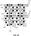
- FIG. 2A is a schematic illustrating a top view through a stacked quantum computation device (such as device 100) and showing circuit elements from a first chip aligned with circuit elements from a second chip, discussed in more detail with reference to FIG. 1B .
- the first chip includes an array of superconducting qubits (e.g., qubits 222a, 222b).
- the second chip includes wiring elements 230, qubit readout devices (e.g., 224a, 224b), and qubit control elements. Pads for chip-to-chip interconnects, such as bump bonds, are illustrated as distributed in various locations.
- the wiring elements 230 may include or may be coupled to the qubit control elements.
- the wiring elements 230 on a separate chip may overlap portions of the superconducting qubits on the first chip.
- the qubit readout devices 224a, 224b may include a portion, such as pad elements 226a, 226b (see FIG. 2A ), that overlap a part of a corresponding superconducting qubit (e.g., qubit 222a, 222b, respectively) formed on the first chip when the first chip is bonded to the second chip.
- the qubit readout devices 224a, 224b also may include resonator elements 228a, 228b, respectively that do not overlap the qubits on the first chip.
- Resonator elements 228a and 228b are illustrated in FIGS. 1B and 2A as solid pads but may include, e.g., a transmission line resonator (e.g., a distributed element resonator or a lumped element resonator), such as a co-planar waveguide.
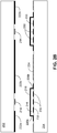
- FIG. 2B is a schematic illustrating a cross-sectional view through an exemplary stacked quantum computation device, such as the device shown in FIG. 2A .
- the stacked device includes a first chip 202 bonded (e.g., bump bonded) to a second chip 204.
- the substrates of the first chip 202 and the second chip 204 may be formed from, e.g., a low loss dielectric suitable for quantum computing circuit elements, such as a silicon or sapphire wafer.
- the ground planes and qubits may be formed, at least in part, from superconductor metal film, such as Al.
- the portions 222a, 222b, 222c may correspond to elongated arms of the neighboring superconducting qubits (e.g., in the case the qubits include xmon qubits).
- the superconductor ground planes 214 are located between the neighboring superconducting qubits.
- the second chip 204 includes wiring elements 230, which may include qubit control elements (e.g., qubit Z-control elements and/or qubit XY-control elements).
- the second chip 204 also may include one or more qubit readout devices, which may include elements such as a resonator element (e.g., 228a, 228b) and a pad element (e.g., 226a, 226b) as illustrated in FIG 2A .
- a pad element 226a is shown in FIG. 2B overlapping a portion of qubit 222b. In the cross-section illustrated in FIG.
- wiring elements 230 on the second chip 204 pass at least partially underneath portions 222a, 222b, 222c, of superconducting qubits located on the first chip 202.
- the wiring elements are covered by a shielding layer 218, which blocks fields from the qubits and wiring elements from interfering with one another. Such interference may cause the superconducting qubits to dampen and decohere.
- a dielectric layer 216 is provided on the wiring elements 230.
- the dielectric layer 216 may include lossy dielectrics, such as tetraethyl orthosilicate (TEOS), silicon dioxide, or silicon nitride.
- a "lossy" dielectric may be defined relative to a quality factor (Q) of a device which incorporates the dielectric. For example, for a device having a quality factor Q, a dielectric of that device may be considered lossy if the dielectric has a loss tangent larger than 1/Q.
- a lossy dielectric material includes, e.g., a dielectric material with a loss tangent at microwave frequencies (between about 1 and about 10 GHz) that is above at least le-4 or at least le-5.
- the lossy dielectric material may be deposited, e.g., using a plasma deposition process. A thickness of a deposited dielectric material can range between about 50 nm and about 2000 nm.
- the shielding layer 218 includes a superconductor material, such as A1, and may be deposited over the dielectric layer 216 to cover the dielectric layer 216.
- the shielding layer 218 may be deposited by, e.g. a physical vapor deposition process.
- a surface of the dielectric layer 216 is completely covered by the shielding layer 218, including the sidewalls of the dielectric layer 216 (e.g., sidewalls 220a and 220b), effectively encapsulating the surface of the dielectric layer 216 that is not formed on the second chip 204.
- the shielding layer covers just the surface of the dielectric layer facing the first chip 202.
- a thickness of superconductor layer e.g., metal layer
- the lossy dielectric may lead to a low intrinsic quality factor Qi for the qubit readout devices 224, and thus coherence that is too low for the qubit readout elements to function properly.
- a dielectric layer is not provided on the readout devices 224. For example, after forming dielectric layer 216 on chip 204, portions of the dielectric layer 216 may be removed to form an opening through which the qubit readout device 224 is exposed.
- wiring elements 230 are shown in FIG. 2B as a single layer of superconductor material, multiple layers of superconductor material may be formed as part of wiring elements 230, where the multiple layers of superconductor material are embedded within dielectric material.
- An unclaimed example of a multi-layer stack is described with reference to FIG. 6 .
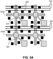
- FIG. 3A is a schematic illustrating a top view through a stacked quantum computation device (such as device 100) and showing circuit elements from a first chip aligned with circuit elements from a second chip, as discussed herein with respect to FIGS. 1B and 2A .
- the section identified by dashed line B-B indicates a region in which the qubit control elements couple to the superconducting qubits of the first chip.
- FIG. 3B is a schematic illustrating a cross-sectional view through a stacked quantum computation device, such as the device shown in FIG. 3A .
- the stacked device includes a first chip 302 bonded (e.g., bump bonded) to a second chip 304.
- the substrates of the first chip 302 and the second chip 304 may be formed from, e.g., a low loss dielectric suitable for quantum computing circuit elements, such as a silicon or sapphire wafer.
- the cross-section illustrated in FIG. 3B includes a portion 322a of a superconducting qubit, as well as portions 314 of ground planes formed on the first chip 302.
- the ground planes and qubits may be formed, at least in part, from superconductor metal film, such as Al.
- the portion 322a may correspond to an elongated arm of a superconducting qubit (e.g., in the case the qubits include xmon qubits).
- Bump bonds 320 e.g., superconductor bump bonds
- the second chip 304 includes wiring elements 330, which may include qubit control elements (e.g., qubit Z-control elements and/or qubit XY-control elements), formed on the second chip 304.
- the second chip 304 also may include one or more qubit readout devices 324, such as a resonator element or a pad element.
- the wiring elements 330 may be covered by a shielding layer 318 (e.g., a superconductor film such as an Al film), which isolates the wiring elements 330 from the qubits on the first chip 302.
- a dielectric layer 316 is provided on the wiring elements 330.
- the dielectric layer 316 may include lossy dielectrics, such as tetraethyl orthosilicate (TEOS), silicon dioxide, or silicon nitride.
- TEOS tetraethyl orthosilicate
- FIG. 3B illustrates a region in which the shielding is absent so that a qubit control element on the second chip 304 may couple (e.g., capacitively couple) to a qubit on the first chip 302.
- via 326 is formed within the dielectric layer 316. Via 326 extends from a surface of the dielectric layer 316 through the dielectric layer 316 to wiring element 330 and may be filled with a superconductor metal, such as Al, to form a via interconnect.
- a contact pad 328 is formed on via interconnect 326 and serves as a qubit control element.
- the contact pad 328 may be surrounded laterally by the shielding layer 318, but physically separate from the shielding layer 318 (e.g., a gap may be located between the shielding layer 318 and the exposed contact pad 328).
- the contact pad 328 also may be formed from a superconductor metal, such as an Al thin film.
- the contact pad 328 on the second chip 304 is aligned under or over a portion of superconducting qubit (e.g., qubit 322a) on the first chip 302 such that the contact pad 328 overlaps (e.g., directly faces) the superconducting qubit when the two chips are bonded together.
- the contact pad 328 on the second chip 304 is displaced laterally from a portion of superconducting qubit on the first chip 302 such that the contact pad 328 does not overlap the superconducting qubit when the two chips are aligned and bonded together.
- a dielectric layer is not provided on the qubit readout device 324 to preserve the coherence of the qubit readout device 324.
- a portion of the qubit readout element is aligned with superconductor ground plane 314 of the first chip 302.
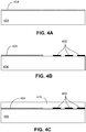
- FIGS. 4A-4F are schematics illustrating an exemplary process for fabricating a chip (as second chip 204 or chip 304) that will have qubit readout and control elements for a stacked quantum computing device.
- a chip 404 is provided.
- Chip 404 may be formed from a dielectric substrate, e.g., a silicon or sapphire substrate.
- a first superconductor layer 424 is provided on a surface of the chip 404.
- Superconductor layer 424 may include, e.g., aluminum, niobium-titanium, or other materials or alloys having superconducting properties below a superconducting critical temperature.
- the superconductor layer 424 may be deposited using, e.g., a physical vapor deposition process, among other techniques.
- the superconductor layer 424 is patterned. Patterning may entail selectively removing portions of already deposited superconductor material through, e.g., selective etching or a lift-off process. Alternatively, the layer 424 may be patterned by depositing the superconductor material through one or more masks in the process step depicted by FIG. 4A . Patterning the superconductor layer 424 defines distinct structures, such as one or more wiring elements 430.
- a dielectric layer 416 then is provided on the superconductor layer 424.
- the dielectric layer 416 may be deposited using, e.g., a physical vapor deposition process or a plasma deposition process, among other techniques.
- the dielectric layer 416 can include dielectric materials such as TEOS, silicon dioxide, or silicon nitride.
- the deposited dielectric is a lossy material, having a loss tangent at microwave frequencies above at least le-4 or at least le-5 at frequencies between about 1 GHz and about 10 GHz.
- dielectric layer 416 is patterned to remove portions of dielectric material. For example, in some implementations, portions of the dielectric layer 416 are removed to expose superconductor layer 424 in regions where a qubit readout element will be formed. In some implementations, portions of the dielectric layer 416 are removed to provide a via 426 to wiring elements 430 in regions where a qubit control element will be formed. In some implementations, dielectric layer 416 deposited over the superconductor layer 424 is not removed during the patterning step. Patterning dielectric layer 416 may include selectively etching the dielectric layer, among other techniques.
- a second superconductor layer 418 is provided.
- the second superconductor layer may be deposited, e.g., on a surface of the dielectric layer 416, on a surface of the superconductor layer 424, and on the exposed chip 404 (e.g., exposed dielectric substrate).
- the second superconductor layer may be deposited, e.g., on a surface of the dielectric layer 416.
- the second superconductor layer 418 is deposited within the via 426 to form a via interconnect.
- the second superconductor layer 418 is deposited on a sidewall 415 of the dielectric layer 416.
- the second superconductor layer 418 may be the same or different superconductor material as first superconductor layer 424.
- the second superconductor layer 424 may be deposited, e.g., by a physical vapor deposition process, among other techniques.
- the second superconductor layer 418 is patterned.
- both the second superconductor layer 418 and the superconductor layer 424 are selectively patterned simultaneously to form a circuit element, such as a qubit readout element 450 (e.g., a co-planar waveguide qubit readout resonator).
- a qubit readout element 450 e.g., a co-planar waveguide qubit readout resonator
- the second superconductor layer 418 is patterned and a portion of the second superconductor layer 418 and a portion of the dielectric layer 416 are removed in a same or in subsequent steps, such that a portion of a sidewall 415 of the dielectric layer 416 is exposed and a portion of superconductor layer 424 is exposed.
- a portion of exposed dielectric layer sidewall 415 may be exposed (uncapped by superconductor layer 418) while still achieving high quality (e.g., better coherence properties) for the superconducting qubit and qubit readout element.
- the exposed superconductor layer 424 may be selectively patterned to form a circuit element, such as a qubit readout element.
- the second superconductor layer 418 is selectively patterned to define a qubit control element (e.g., a qubit Z-control element or a qubit XY control element).
- a qubit control element e.g., a qubit Z-control element or a qubit XY control element.
- second superconductor layer 418 is patterned in FIG. 4F to define a contact pad 428 that forms part of a qubit control element 460.
- the patterning removes portions of the second superconductor layer 418 to electrically isolate layer 418 from the contact pad 428 and from the qubit readout element 424.
- the patterned layer 418 also serves as the shielding layer.
- the chip 404 may be aligned and bonded (e.g., through flip-chip bonding) to a separate chip containing superconducting qubits (e.g., such as chip 202 or chip 302).
- a separate chip containing superconducting qubits e.g., such as chip 202 or chip 302
- the fabrication process described with respect to FIGS. 4A-4F may result in the qubit readout element exhibiting better coherence properties.
- the patterning of the qubit readout element is left until the last or close to the last process step. In this way, damage to the interfaces from etching steps as well as residue can be reduced, resulting in improved qubit readout element quality factor.
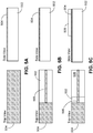
- FIGS. 5A-5E are schematics illustrating an exemplary process for fabricating a chip for a stacked quantum computing device, as viewed from a top-view and side view at different steps of a fabrication process.
- a chip 502 is provided.
- Chip 502 may be formed from a dielectric substrate, e.g., a silicon or sapphire substrate.
- a first superconductor layer 504 is deposited on a surface of chip 502.
- Superconductor layer 504 may include, e.g., aluminum, niobium-titanium, or other materials or alloys having superconducting properties below a superconducting critical temperature.
- the superconductor layer 504 may be deposited using, e.g., a physical vapor deposition process, among other techniques.
- the superconductor layer 504 is patterned. Patterning may entail selectively removing portions of already deposited superconductor material through, e.g., selective etching or a lift-off process. Alternatively, the layer 504 may be patterned by depositing the superconductor material through one or more masks in the process step depicted by FIG. 5A.
- FIG. 5B defines distinct structures defined by a patterning process, including one or more control wires 506. Portions of the first superconductor layer 504 that are removed expose the underlying chip 502.
- a dielectric layer 508 then is formed on the superconductor layer 504 and on chip 502.
- Dielectric layer 508 may be deposited using, e.g., a physical vapor deposition process or a plasma deposition process, among other techniques.
- the dielectric layer 508 can include dielectric materials such as TEOS, silicon dioxide, or silicon nitride.
- the deposited dielectric is a lossy material, having a loss tangent at microwave frequencies above at least le-4 or at least le-5 at frequencies between about 1 GHz and about 10 GHz.
- the dielectric layer 508 may be patterned (e.g., through an etch or lift-off process) to expose a region in which the qubit readout element will be formed.
- a second superconductor layer 510 is formed on the patterned dielectric layer 508, the first superconductor layer 504 (including, e.g., the control wire 506) and the chip 502.
- the deposition may be a conformal deposition, such that the second superconductor layer 510 covers the sidewalls of the dielectric layer 508.
- the second superconductor layer 5 10 can be of a same superconductor material as first superconductor layer 504, or can be of a different superconductor material.
- the first superconductor layer 504 and the second superconductor layer 5 10 then are patterned as shown in FIG. 5E .
- the second superconductor layer 510 and the first superconductor layer 504 are selectively patterned to define different structures.
- the second superconductor layer 510 may be patterned to expose the control wire 506, a portion of the dielectric layer 508 and a portion of the first superconductor layer 504.
- the first superconductor layer 504 may be patterned to define a qubit readout element 518.
- the patterning process can occur in a single etching step or multiple etching steps.
- the dielectric layer 508 is patterned to expose a portion of the dielectric layer 508.
- sidewall 512 is exposed through a patterning step.
- the chip may be aligned and bonded (e.g., through flip-chip bonding) to a separate chip containing superconducting qubits (e.g., such as chip 202 or chip 302).
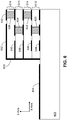
- FIG. 6 is a schematic illustrating a side view of an exemplary chip to be used in a stacked quantum computing device.
- Chip 602 may include one or more qubit readout elements, qubit control elements, and/or wiring elements.
- Chip 602 may be formed, in part, from material having a relatively high loss (e.g., having a loss tangent of at least about le-4 or at least about le-5 at frequencies between about 1 GHz and about 10 GHz).
- Chip 602 may be aligned and bonded to a chip that includes superconducting qubits to provide a stacked quantum computation device, such as device 100.
- chip 602 may be formed from a dielectric substrate. (e.g., single crystal silicon or sapphire) on which is formed a first layer 604 of superconductor material (e.g., an Al thin film).
- the first layer 604 of superconductor material may be patterned to define, e.g., one or more qubit readout elements, qubit control elements and/or wiring elements.
- Additional layers e.g., layers 606, 608, 610) of superconductor material (e.g., Al) arranged in a stack over the portions of the first superconductor layer 604 may be formed on chip 602.
- the layers 606, 608, 610 may also be patterned to define wiring elements and/or qubit control elements.
- the layers 604, 606, 608, and 610 of superconductor material in the stack may be separated from one another by corresponding layers (e.g., 612, 614, 616, 618) of dielectric material.
- the dielectric material may include lossy dielectrics, such as, e.g., TEOS, silicon dioxide, or silicon nitride.
- a microstrip geometry where two superconductor layers are separated by a dielectric layer (e.g., superconductor layers 610 and 608, separated by dielectric layer 616) may be formed on chip 602.
- a stripline geometry where three superconductor layers are separated by two dielectric layers (e.g., a layer stack including superconductor layer 606, dielectric layer 614, superconductor layer 608, dielectric layer 616, and superconductor layer 610) such that one superconductor signal layer (e.g., superconductor layer 608) is sandwiched between two superconductor layers acting as ground layers (e.g., superconductor layers 606 and 610) may be formed on chip 602.
- multi-layer microstrip geometries, multi-layer stripline geometries, or a combination thereof may be formed on chip 602.
- One or more of the different layers of superconductor material may be electrically coupled to one another through one or more via interconnects (e.g., via interconnect 620, 622, 624, 626).
- via interconnects 620, 622, 624, 626 may be fabricated in a similar manner as the via interconnects 426 detailed in FIGS. 4A-4F .
- the vias are filled with superconductor material (e.g., aluminum) to form the via interconnects.
- the vias may be filled using, e.g., a physical vapor deposition process.
- the location of the via interconnects may depend on the desired routing layout of the wiring elements and the qubit control elements.
- a top layer 628 of superconductor material may be patterned to define a qubit control element 630 (e.g., a qubit Z-control element or a qubit XY control element) and a shielding layer 632.
- the shielding layer 632 may isolate electromagnetic fields from the wiring elements and from qubits provided on a separate chip from interfering with one another.
- the top layer 628 of superconductor material also is deposited to cover the sidewalls of the dielectric layers 612, 614, 616, and 618.
- a superconductor (alternatively superconducting) material can be understood as material that exhibits superconducting properties at or believe a superconducting critical temperature.
- superconducting material include aluminum (superconductive critical temperature of 1.2 kelvin) and niobium (superconducting critical temperature of 9.3 kelvin).
- An example of a superconductor material that can be used in the formation of quantum computing circuit elements is aluminum.
- Aluminum may be used in combination with a dielectric to establish Josephson junctions, which are a common component of quantum computing circuit elements.
- Examples of quantum computing circuit elements that may be formed with aluminum include circuit elements such as superconducting co-planar waveguides, quantum LC oscillators, qubits (e.g., flux qubits or charge qubits), or superconducting quantum interference devices (SQUIDs) (e.g., RF-SQUID or DC-SQUID), among others.
- qubits e.g., flux qubits or charge qubits
- SQUIDs superconducting quantum interference devices
- Aluminum may also be used in the formation of superconducting classical circuit elements that are interoperable with superconducting quantum computing circuit elements as well as other classical circuit elements based on complementary metal oxide semiconductor (CMOS) circuity.
- Examples of classical circuit elements that may be formed with aluminum include rapid single flux quantum (RSFQ) devices, reciprocal quantum logic (RQL) devices and ERSFQ devices, which are an energy-efficient version of RSFQ that does not use bias resistors.
- RSFQ rapid single flux quantum
- RQL reciprocal quantum logic
- ERSFQ devices which are an energy-efficient version of RSFQ that does not use bias resistors.
- Other classical circuit elements may be formed with aluminum as well.
- the classical circuit elements may be configured to collectively carry out instructions of a computer program by performing basic arithmetical, logical, and/or input/output operations on data, in which the data is represented in analog or digital form.
- Processes described herein may entail the deposition of one or more materials, such as superconductors, dielectrics and/or metals. Depending on the selected material, these materials may be deposited using deposition processes such as chemical vapor deposition, physical vapor deposition (e.g., evaporation or sputtering), or epitaxial techniques, among other deposition processes. Processes described herein may also entail the removal of one or more materials from a device during fabrication. Depending on the material to be removed, the removal process may include, e.g., wet etching techniques, dry etching techniques, or lift-off processes.
- superconducting qubits are represented as xmon qubits.
- the subject matter of the disclosure may be implemented with other suitable superconducting qubits.
- superconducting qubits include gmon qubits, transmon qubits, or fluxmon qubits, among other types of qubits.
- quantum computational systems may include, but is not limited to, quantum computers, quantum information processing systems, quantum cryptography systems, or quantum simulators.
- quantum information and quantum data refer to information or data that is carried by, held or stored in quantum systems, where the smallest non-trivial system is a qubit, e.g., a system that defines the unit of quantum information.
- qubit encompasses all quantum systems that may be suitably approximated as a two-level system in the corresponding context.
- Such quantum systems may include multi-level systems, e.g., with two or more levels.
- such systems can include atoms, electrons, photons, ions or superconducting qubits.
- the computational basis states are identified with the ground and first excited states, however it is understood that other setups where the computational states are identified with higher level excited states are possible.
- quantum memories are devices that can store quantum data for a long time with high fidelity and efficiency, e.g., light-matter interfaces where light is used for transmission and matter for storing and preserving the quantum features of quantum data such as superposition or quantum coherence.
- Quantum computing circuit elements may be used to perform quantum processing operations. That is, the quantum computing circuit elements may be configured to make use of quantum-mechanical phenomena, such as superposition and entanglement, to perform operations on data in a non-deterministic manner. Certain quantum computing circuit elements, such as qubits, may be configured to represent and operate on information in more than one state simultaneously.
- superconducting quantum computing circuit elements that may be formed with the processes disclosed herein include circuit elements such as co-planar waveguides, quantum LC oscillators, qubits (e.g., flux qubits or charge qubits), superconducting quantum interference devices (SQUIDs) (e.g., RF-SQUID or DC-SQUID), inductors, capacitors, transmission lines, ground planes, among others.
- qubits e.g., flux qubits or charge qubits
- SQUIDs superconducting quantum interference devices
- inductors e.g., RF-SQUID or DC-SQUID
- capacitors e.g., transmission lines, ground planes, among others.
- classical circuit elements generally process data in a deterministic manner.
- Classical circuit elements may be configured to collectively carry out instructions of a computer program by performing basic arithmetical, logical, and/or input/output operations on data, in which the data is represented in analog or digital form.
- classical circuit elements may be used to transmit data to and/or receive data from the quantum computing circuit elements through electrical or electromagnetic connections.
- Unclaimed examples of classical circuit elements that may be formed with the processes disclosed herein include rapid single flux quantum (RSFQ) devices, reciprocal quantum logic (RQL) devices and ERSFQ devices, which are an energy-efficient version of RSFQ that does not use bias resistors.
- Other classical circuit elements may be formed with the processes disclosed herein as well.
- the superconducting circuit elements are cooled down within a cryostat to temperatures that allow a superconductor material to exhibit superconductor properties.
Landscapes
- Engineering & Computer Science (AREA)
- Physics & Mathematics (AREA)
- Theoretical Computer Science (AREA)
- General Physics & Mathematics (AREA)
- Data Mining & Analysis (AREA)
- Computing Systems (AREA)
- Evolutionary Computation (AREA)
- Computational Mathematics (AREA)
- Mathematical Analysis (AREA)
- Mathematical Optimization (AREA)
- Pure & Applied Mathematics (AREA)
- Condensed Matter Physics & Semiconductors (AREA)
- General Engineering & Computer Science (AREA)
- Mathematical Physics (AREA)
- Software Systems (AREA)
- Artificial Intelligence (AREA)
- Superconductor Devices And Manufacturing Methods Thereof (AREA)
- Health & Medical Sciences (AREA)
- Electromagnetism (AREA)
- Toxicology (AREA)
Claims (15)
- Vorrichtung, umfassend:einen ersten Chip (202; 302), umfassend:ein erstes dielektrisches Substrat undein supraleitendes Qubit (222a, 222b; 322a, 322b) auf dem ersten dielektrischen Substrat;einen zweiten Chip (204; 304), der mit dem ersten Chip verbunden ist, der zweite Chip umfassend:dadurch gekennzeichnet, dass die Abschirmschicht so angeordnet ist, dass sie das Übersprechen zwischen dem Steuerdraht auf dem zweiten Chip und dem supraleitenden Qubit auf dem ersten Chip reduziert, indem elektromagnetische Felder von dem Steuerdraht und von dem supraleitenden Qubit gegeneinander isoliert werden.ein zweites dielektrisches Substrat,ein Qubit-Ausleseelement (224, 224a, 224b; 324, 324a, 324b) auf dem zweiten dielektrischen Substrat,einen Steuerdraht (230; 330) auf dem zweiten dielektrischen Substrat,eine dielektrische Schicht (216; 316), die den Steuerdraht bedeckt, undeine Abschirmschicht (218; 328), die die dielektrische Schicht bedeckt,
- Vorrichtung nach Anspruch 1, wobei die dielektrische Schicht (216; 316) eine Öffnung umfasst, durch die das Qubit-Ausleseelement (224, 224a, 224b; 324, 324a, 324b) freigelegt wird.
- Vorrichtung nach Anspruch 1 oder Anspruch 2, wobei die dielektrische Schicht (216; 316) ein dielektrisches Material mit einer Verlusttangente größer als etwa 10-5 bei einer Frequenz zwischen etwa 1 GHz und etwa 10 GHz umfasst.
- Vorrichtung nach einem der vorhergehenden Ansprüche, wobei das supraleitende Qubit (222a, 222b; 322a, 322b) einen Auslesebereich umfasst, und
wobei das Qubit-Ausleseelement (224a, 224b; 324a, 324b) den Auslesebereich des Qubits überlappt. - Vorrichtung nach Anspruch 4, wobei das Qubit-Ausleseelement (224a, 224b; 324a, 324b) ein Resonatorelement (228a, 228b) umfasst, das elektrisch mit einem Anschlusselement gekoppelt ist, und wobei das Anschlusselement den Auslesebereich des Qubits überlappt, ohne dass das Resonatorelement den Auslesebereich des Qubits überlappt.
- Vorrichtung nach Anspruch 4 oder Anspruch 5, wobei der erste Chip (202; 302) eine Supraleiter-Masseebene (214; 314) umfasst und wobei das Resonatorelement die Supraleiter-Masseebene überlappt.
- Vorrichtung nach einem der vorhergehenden Ansprüche, wobei die dielektrische Schicht (316) umfasst:einen Durchgang (326), der sich von einer Oberfläche der dielektrischen Schicht durch die dielektrische Schicht zu dem Steuerdraht (330) erstreckt;eine Zwischenverbindung (326) innerhalb des Durchgangs und elektrisch mit dem Steuerdraht gekoppelt; undeinen Steuerkontakt (328) auf der Oberfläche der dielektrischen Schicht und elektrisch mit der Zwischenverbindung gekoppelt.
- Vorrichtung nach Anspruch 7, wobei:der Steuerkontakt (328) seitlich von der Abschirmschicht umgeben und physisch von der Abschirmschicht getrennt ist; und/oderder Steuerkontakt das supraleitende Qubit überlappt; und/oderder Steuerkontakt seitlich von dem supraleitenden Qubit verschoben wird, ohne das supraleitende Qubit zu überlappen.
- Vorrichtung nach einem der vorhergehenden Ansprüche, wobei die Abschirmschicht eine Seitenwand der dielektrischen Schicht bedeckt und/oder jedes von dem Qubit-Ausleseelement, dem Steuerdraht und der Abschirmschicht ein Supraleiter ist.
- Vorrichtung nach einem der vorhergehenden Ansprüche, wobei der zweite Chip eine Vielzahl von Steuerdrähten und eine Vielzahl von dielektrischen Schichten umfasst,
wobei die Vielzahl von Steuerdrähten in die Vielzahl von dielektrischen Schichten eingebettet sind, und
wobei die Abschirmschicht die Vielzahl von dielektrischen Schichten bedeckt. - Vorrichtung nach einem der vorhergehenden Ansprüche, wobei der erste Chip mit dem zweiten Chip höckergebondet ist.
- Verfahren, umfassend:Bereitstellen eines ersten Chips (202, 302), wobei der erste Chip ein erstes dielektrisches Substrat und ein supraleitendes Qubit (222a, 222b; 322a, 322b) auf dem ersten dielektrischen Substrat umfasst;Bereitstellen eines zweiten Chips (204, 304), wobei der zweite Chip ein zweites dielektrisches Substrat, ein Qubit-Ausleseelement (224, 224a, 224b; 324, 324a, 324b) auf dem zweiten dielektrischen Substrat, einen Steuerdraht (230; 330) auf dem zweiten dielektrischen Substrat, eine dielektrische Schicht (216; 316), die den Steuerdraht abdeckt, und eine Abschirmschicht (218; 328), die die dielektrische Schicht abdeckt, umfasst; undBonden des ersten Chips mit dem zweiten Chip mit Supraleiter-Höcker-Bonds (320),dadurch gekennzeichnet, dass die Abschirmschicht so angeordnet ist, dass sie Übersprechen zwischen dem Steuerdraht auf dem zweiten Chip und dem supraleitenden Qubit auf dem ersten Chip reduziert, indem elektromagnetische Felder von dem Steuerdraht und von dem supraleitenden Qubit von einer gegenseitigen Störung isoliert werden.
- Verfahren nach Anspruch 12, wobei das Bereitstellen des zweiten Chips (204, 304) Folgendes umfasst:Bereitstellen des zweiten dielektrischen Substrats;Bilden einer ersten Supraleiterschicht (424) auf dem zweiten dielektrischen Substrat;Strukturieren der ersten Supraleiterschicht, sodass die erste Supraleiterschicht einen Steuerdraht (430) umfasst;Bilden der dielektrischen Schicht (416) auf der ersten Supraleiterschicht, die den Steuerdraht umfasst;Strukturieren der dielektrischen Schicht, um eine strukturierte dielektrische Schicht bereitzustellen;Bilden einer zweiten Supraleiterschicht (418) auf der strukturierten dielektrischen Schicht; undStrukturieren der zweiten Supraleiterschicht und der ersten Supraleiterschicht, um das Qubit-Ausleseelement (450) und die Abschirmschicht (418) bereitzustellen.
- Verfahren nach Anspruch 13, wobei das Strukturieren der dielektrischen Schicht (416) das Ausbilden eines Durchgangs (426) in der dielektrischen Schicht umfasst, um einen Abschnitt des Steuerdrahts (430) freizulegen, wobei sich der Durchgang von einer Oberfläche der dielektrischen Schicht zu dem Abschnitt des Steuerdrahts erstreckt, der freigelegt ist, wobei das Ausbilden der zweiten Supraleiterschicht (418) das Ausbilden einer Zwischenverbindung (426) innerhalb des Durchgangs umfasst, wobei die Zwischenverbindung den Abschnitt des Steuerdrahts kontaktiert, der freigelegt ist;
optional wobei das Strukturieren der zweiten Supraleiterschicht das Bilden eines Steuerkontakts auf der Oberfläche der dielektrischen Schicht umfasst; und/oder
ferner umfassend das Ausrichten des zweiten dielektrischen Substrats auf den ersten Chip vor dem Bonden, sodass das Qubit-Ausleseelement (450) das supraleitende Qubit überlappt. - Vorrichtung nach Anspruch 1, ferner umfassend:eine erste Supraleiterschicht (424) auf dem zweiten dielektrischen Substrat, wobei ein erster Bereich der ersten Supraleiterschicht das Qubit-Ausleseelement (450) bildet und ein zweiter Bereich der ersten Supraleiterschicht ein Qubit-Steuerelement (430) zum Koppeln mit und Steuern des supraleitenden Qubits bildet, wobei das Qubit-Steuerelement mit dem Steuerdraht gekoppelt ist;wobei die dielektrische Schicht (416) auf dem zweiten Bereich der ersten Supraleiterschicht angeordnet ist;die Quantenrechenschaltungsvorrichtung ferner umfassend:einen Durchgang (426) in der dielektrischen Schicht, um einen Abschnitt des Qubit-Steuerelements freizulegen, wobei sich der Durchgang von einer Oberfläche der dielektrischen Schicht zu dem Abschnitt des Qubit-Steuerelements erstreckt, der freigelegt ist;eine zweite Supraleiterschicht (418) auf der dielektrischen Schicht, wobei die zweite Supraleiterschicht eine Zwischenverbindung innerhalb des Durchgangs bildet, wobei die Zwischenverbindung den Abschnitt des Qubit-Steuerelements kontaktiert, der freigelegt ist, und wobei die zweite Supraleiterschicht die Abschirmschicht (418) bildet.
Priority Applications (1)
| Application Number | Priority Date | Filing Date | Title |
|---|---|---|---|
| EP21153943.2A EP3852021B1 (de) | 2017-03-13 | 2017-12-15 | Integration von schaltungselementen in eine gestapelte quanten-computing-vorrichtung |
Applications Claiming Priority (2)
| Application Number | Priority Date | Filing Date | Title |
|---|---|---|---|
| US201762470694P | 2017-03-13 | 2017-03-13 | |
| PCT/US2017/066574 WO2018169585A1 (en) | 2017-03-13 | 2017-12-15 | Integrating circuit elements in a stacked quantum computing device |
Related Child Applications (2)
| Application Number | Title | Priority Date | Filing Date |
|---|---|---|---|
| EP21153943.2A Division-Into EP3852021B1 (de) | 2017-03-13 | 2017-12-15 | Integration von schaltungselementen in eine gestapelte quanten-computing-vorrichtung |
| EP21153943.2A Division EP3852021B1 (de) | 2017-03-13 | 2017-12-15 | Integration von schaltungselementen in eine gestapelte quanten-computing-vorrichtung |
Publications (2)
| Publication Number | Publication Date |
|---|---|
| EP3580702A1 EP3580702A1 (de) | 2019-12-18 |
| EP3580702B1 true EP3580702B1 (de) | 2021-03-17 |
Family
ID=60935992
Family Applications (2)
| Application Number | Title | Priority Date | Filing Date |
|---|---|---|---|
| EP17825709.3A Active EP3580702B1 (de) | 2017-03-13 | 2017-12-15 | Integration von schaltungselementen in eine gestapelte quanten-computing-vorrichtung |
| EP21153943.2A Active EP3852021B1 (de) | 2017-03-13 | 2017-12-15 | Integration von schaltungselementen in eine gestapelte quanten-computing-vorrichtung |
Family Applications After (1)
| Application Number | Title | Priority Date | Filing Date |
|---|---|---|---|
| EP21153943.2A Active EP3852021B1 (de) | 2017-03-13 | 2017-12-15 | Integration von schaltungselementen in eine gestapelte quanten-computing-vorrichtung |
Country Status (8)
| Country | Link |
|---|---|
| US (4) | US11436516B2 (de) |
| EP (2) | EP3580702B1 (de) |
| JP (1) | JP6810280B2 (de) |
| KR (1) | KR102217205B1 (de) |
| CN (2) | CN118133978A (de) |
| AU (1) | AU2017404536B2 (de) |
| CA (1) | CA3056596C (de) |
| WO (1) | WO2018169585A1 (de) |
Cited By (1)
| Publication number | Priority date | Publication date | Assignee | Title |
|---|---|---|---|---|
| US12475396B2 (en) | 2022-09-14 | 2025-11-18 | International Business Machines Corporation | Qubit and readout overlap optimization via dipole orientation |
Families Citing this family (58)
| Publication number | Priority date | Publication date | Assignee | Title |
|---|---|---|---|---|
| WO2013180780A2 (en) | 2012-03-08 | 2013-12-05 | D-Wave Systems Inc. | Systems and methods for fabrication of superconducting integrated circuits |
| US9971970B1 (en) * | 2015-04-27 | 2018-05-15 | Rigetti & Co, Inc. | Microwave integrated quantum circuits with VIAS and methods for making the same |
| US11038095B2 (en) | 2017-02-01 | 2021-06-15 | D-Wave Systems Inc. | Systems and methods for fabrication of superconducting integrated circuits |
| AU2017404530B2 (en) | 2017-03-13 | 2020-05-14 | Google Llc | Integrating circuit elements in a stacked quantum computing device |
| US11121301B1 (en) | 2017-06-19 | 2021-09-14 | Rigetti & Co, Inc. | Microwave integrated quantum circuits with cap wafers and their methods of manufacture |
| US10811588B2 (en) * | 2018-08-06 | 2020-10-20 | International Business Machines Corporation | Vertical dispersive readout of qubits of a lattice surface code architecture |
| CN109494218B (zh) * | 2018-09-30 | 2021-07-30 | 华东计算技术研究所(中国电子科技集团公司第三十二研究所) | 双面超导量子芯片 |
| US10720563B1 (en) | 2018-11-13 | 2020-07-21 | Google Llc | Quantum processor design to increase control footprint |
| US20200152851A1 (en) | 2018-11-13 | 2020-05-14 | D-Wave Systems Inc. | Systems and methods for fabricating superconducting integrated circuits |
| US10692795B2 (en) * | 2018-11-13 | 2020-06-23 | International Business Machines Corporation | Flip chip assembly of quantum computing devices |
| US12102017B2 (en) | 2019-02-15 | 2024-09-24 | D-Wave Systems Inc. | Kinetic inductance for couplers and compact qubits |
| US10840428B2 (en) * | 2019-03-07 | 2020-11-17 | International Business Machines Corporation | Scalable quantum devices with vertical coaxial resonators |
| US10796069B1 (en) * | 2019-06-06 | 2020-10-06 | International Business Machines Corporation | Bump connection placement in quantum devices in a flip chip configuration |
| US10944039B2 (en) * | 2019-06-19 | 2021-03-09 | International Business Machines Corporation | Fabricating transmon qubit flip-chip structures for quantum computing devices |
| JP7427914B2 (ja) * | 2019-10-30 | 2024-02-06 | 日本電気株式会社 | 超伝導回路装置、スペーサ、及び超伝導回路装置の製造方法 |
| US12367412B2 (en) | 2019-12-05 | 2025-07-22 | 1372934 B.C. Ltd. | Systems and methods for fabricating flux trap mitigating superconducting integrated circuits |
| US11568296B2 (en) * | 2019-12-11 | 2023-01-31 | International Business Machines Corporation | Highway jumper to enable long range connectivity for superconducting quantum computer chip |
| US12598922B2 (en) | 2020-01-17 | 2026-04-07 | D-Wave Systems Inc. | Systems and methods for fabricating superconducting integrated circuits |
| US12079634B2 (en) * | 2020-02-18 | 2024-09-03 | Advanced Micro Devices, Inc. | Look-ahead teleportation for reliable computation in multi-SIMD quantum processor |
| US11195799B2 (en) * | 2020-03-31 | 2021-12-07 | International Business Machines Corporation | Hybrid readout package for quantum multichip bonding |
| WO2021231224A1 (en) | 2020-05-11 | 2021-11-18 | D-Wave Systems Inc. | Kinetic inductance devices, methods for fabricating kinetic inductance devices, and articles employing the same |
| WO2021245949A1 (ja) * | 2020-06-05 | 2021-12-09 | 日本電気株式会社 | 量子デバイス及び量子計算機 |
| JP7528564B2 (ja) * | 2020-06-29 | 2024-08-06 | 日本電気株式会社 | 量子デバイス及びその製造方法 |
| EP3937093B1 (de) * | 2020-07-09 | 2024-09-04 | IQM Finland Oy | Quantenrechenschaltung mit einer vielzahl von chips und verfahren zu deren herstellung |
| US11839167B2 (en) * | 2020-08-25 | 2023-12-05 | Microsoft Technology Licensing, Llc | Individually tunable quantum dots in all-van der waals heterostructures |
| CN111967603B (zh) * | 2020-09-01 | 2022-04-08 | 腾讯科技(深圳)有限公司 | 量子芯片、量子处理器及量子计算机 |
| JP7824610B2 (ja) | 2020-09-15 | 2026-03-05 | シーク, インコーポレイテッド | 超電導量子ビットのための非断熱単一磁束量子(sfq)読出を伴う量子算出システム |
| JP7671463B6 (ja) * | 2020-10-14 | 2025-06-23 | シーク, インコーポレイテッド | 量子コンピューティングシステムにおける量子コンピューティングモジュールと非量子処理モジュールとの間の相互接続 |
| US11469485B2 (en) | 2020-10-21 | 2022-10-11 | International Business Machines Corporation | Embedded microstrip transmission line |
| KR102778201B1 (ko) * | 2020-11-11 | 2025-03-10 | 삼성전자주식회사 | 양자 컴퓨터의 초전도 큐빗 메모리 |
| US12033981B2 (en) * | 2020-12-16 | 2024-07-09 | International Business Machines Corporation | Create a protected layer for interconnects and devices in a packaged quantum structure |
| WO2022143809A1 (zh) * | 2020-12-31 | 2022-07-07 | 合肥本源量子计算科技有限责任公司 | 超导量子芯片结构以及超导量子芯片制备方法 |
| WO2022232717A2 (en) * | 2021-02-17 | 2022-11-03 | Cornell University | Integrated quantum computing with epitaxial materials |
| WO2022178130A1 (en) * | 2021-02-19 | 2022-08-25 | D-Wave Systems Inc. | Systems and methods for fabrication of superconducting integrated circuits with improved coherence |
| JP7641138B2 (ja) * | 2021-03-01 | 2025-03-06 | 株式会社日立製作所 | 量子情報処理装置 |
| CN115050886B (zh) * | 2021-03-09 | 2024-08-16 | 本源量子计算科技(合肥)股份有限公司 | 一种量子芯片及制备方法 |
| CN118339566A (zh) | 2021-06-11 | 2024-07-12 | 西克公司 | 针对超导量子电路的通量偏置的系统和方法 |
| WO2023274548A1 (en) * | 2021-07-01 | 2023-01-05 | MAX-PLANCK-Gesellschaft zur Förderung der Wissenschaften e.V. | Method for producing a solid-state component, solid-state component, quantum component and apparatus for producing a solid-state component |
| CN113420884B (zh) * | 2021-07-14 | 2024-10-25 | 本源量子计算科技(合肥)股份有限公司 | 一种量子芯片、量子计算机及量子芯片制备方法 |
| CN113725208A (zh) * | 2021-08-13 | 2021-11-30 | 中国科学院物理研究所 | 一种三维量子芯片及其制备方法 |
| US12392823B2 (en) | 2021-11-05 | 2025-08-19 | D-Wave Systems Inc. | Systems and methods for on-chip noise measurements |
| JP7782215B2 (ja) | 2021-11-08 | 2025-12-09 | 日本電気株式会社 | 量子デバイス |
| WO2023132063A1 (ja) | 2022-01-07 | 2023-07-13 | 富士通株式会社 | 量子演算装置及び量子演算装置の製造方法 |
| CN114757140B (zh) * | 2022-03-31 | 2024-06-04 | 本源科仪(成都)科技有限公司 | 量子比特版图的布线方法、装置、电子设备及存储介质 |
| EP4503904A4 (de) * | 2022-03-31 | 2025-05-28 | Fujitsu Limited | Quantenvorrichtung und verfahren zur herstellung einer quantenvorrichtung |
| US12393856B2 (en) | 2022-06-29 | 2025-08-19 | Cisco Technology, Inc. | Superconducting quantum architectures |
| CA3263651A1 (en) * | 2022-08-09 | 2024-05-16 | 1372934 B.C. Ltd. | SYSTEMS AND METHODS FOR MANUFACTURING SUPERCONDUCTIVE INTEGRATED CIRCUITS HAVING INVERTED CHIP ARRANGEMENTS WITH HIGH-COHERENCE DEVICES |
| CN115312656B (zh) * | 2022-09-02 | 2025-02-25 | 量子科技长三角产业创新中心 | 一种超导量子约瑟夫森结及其制备方法 |
| EP4633350A4 (de) | 2022-12-07 | 2025-12-31 | Fujitsu Ltd | Quantenbitvorrichtung, verfahren zur herstellung einer quantenbitvorrichtung und verfahren zur messung einer quantenbitvorrichtung |
| US20240194532A1 (en) * | 2022-12-13 | 2024-06-13 | Google Llc | Multi-layer chip architecture and fabrication |
| US20240194661A1 (en) * | 2022-12-13 | 2024-06-13 | Google Llc | Multi-layer chip architecture and fabrication |
| EP4620274A2 (de) | 2022-12-13 | 2025-09-24 | Google LLC | Mehrschicht-chiparchitektur und herstellung |
| JPWO2024185131A1 (de) * | 2023-03-09 | 2024-09-12 | ||
| JPWO2024224493A1 (de) * | 2023-04-25 | 2024-10-31 | ||
| CN119744399A (zh) * | 2023-07-31 | 2025-04-01 | 深圳量旋科技有限公司 | 量子芯片及相关量子计算设备 |
| CN117010509B (zh) * | 2023-07-31 | 2026-01-09 | 本源量子计算科技(合肥)股份有限公司 | 一种串扰的测试结构及其测试和屏蔽方法 |
| JP2025096063A (ja) * | 2023-12-15 | 2025-06-26 | 富士通株式会社 | 量子ビットデバイス及び量子ビットデバイスの製造方法 |
| FI20245066A1 (en) * | 2024-01-23 | 2025-07-24 | Teknologian Tutkimuskeskus Vtt Oy | Elevations connected with indium |
Family Cites Families (28)
| Publication number | Priority date | Publication date | Assignee | Title |
|---|---|---|---|---|
| JPS59138390A (ja) * | 1983-01-28 | 1984-08-08 | Hitachi Ltd | 超電導スイツチング装置 |
| JP2964112B2 (ja) * | 1992-08-11 | 1999-10-18 | セイコーインスツルメンツ株式会社 | 直流駆動型超伝導量子干渉素子 |
| JP2835307B2 (ja) | 1996-01-29 | 1998-12-14 | 株式会社移動体通信先端技術研究所 | 超伝導平面回路 |
| JP5289673B2 (ja) * | 2005-10-21 | 2013-09-11 | 中国電力株式会社 | 超電導接合素子および超電導接合回路 |
| CA2667640C (en) * | 2006-12-01 | 2016-10-04 | D-Wave Systems, Inc. | Superconducting shielding for use with an intergrated circuit for quantum computing |
| US8301214B1 (en) | 2010-01-08 | 2012-10-30 | Hypres, Inc. | System and method for providing multi-conductive layer metallic interconnects for superconducting integrated circuits |
| WO2014168665A2 (en) | 2013-01-18 | 2014-10-16 | Yale University | Methods for making a superconducting device with at least one enclosure |
| EP2946413B1 (de) * | 2013-01-18 | 2022-01-05 | Yale University | Supraleitende vorrichtung mit mindestens einem gehäuse |
| US9219298B2 (en) * | 2013-03-15 | 2015-12-22 | International Business Machines Corporation | Removal of spurious microwave modes via flip-chip crossover |
| JP6894378B2 (ja) * | 2015-02-27 | 2021-06-30 | イェール ユニバーシティーYale University | 平面キュービットを非平面共振器に連結するための技術ならびに関連する系および方法 |
| US9971970B1 (en) * | 2015-04-27 | 2018-05-15 | Rigetti & Co, Inc. | Microwave integrated quantum circuits with VIAS and methods for making the same |
| US9836699B1 (en) * | 2015-04-27 | 2017-12-05 | Rigetti & Co. | Microwave integrated quantum circuits with interposer |
| US10381542B2 (en) * | 2015-04-30 | 2019-08-13 | International Business Machines Corporation | Trilayer Josephson junction structure with small air bridge and no interlevel dielectric for superconducting qubits |
| EP3266063B1 (de) * | 2015-05-14 | 2020-03-18 | D-Wave Systems Inc. | Frequenzmultiplexierter resonatoreingang und/oder -ausgang für eine supraleitende vorrichtung |
| US9524470B1 (en) * | 2015-06-12 | 2016-12-20 | International Business Machines Corporation | Modular array of vertically integrated superconducting qubit devices for scalable quantum computing |
| US10134972B2 (en) * | 2015-07-23 | 2018-11-20 | Massachusetts Institute Of Technology | Qubit and coupler circuit structures and coupling techniques |
| SG11201805577XA (en) * | 2016-01-15 | 2018-07-30 | Univ Yale | Techniques for manipulation of two-qubit quantum states and related systems and methods |
| AU2017404530B2 (en) * | 2017-03-13 | 2020-05-14 | Google Llc | Integrating circuit elements in a stacked quantum computing device |
| WO2018212041A1 (ja) | 2017-05-16 | 2018-11-22 | 国立研究開発法人産業技術総合研究所 | 量子ビットデバイス |
| US10535809B1 (en) * | 2017-08-30 | 2020-01-14 | Rigetti & Co, Inc. | Substrate materials for quantum processors |
| US10305015B1 (en) * | 2017-11-30 | 2019-05-28 | International Business Machines Corporation | Low loss architecture for superconducting qubit circuits |
| US10811588B2 (en) * | 2018-08-06 | 2020-10-20 | International Business Machines Corporation | Vertical dispersive readout of qubits of a lattice surface code architecture |
| US11121302B2 (en) * | 2018-10-11 | 2021-09-14 | SeeQC, Inc. | System and method for superconducting multi-chip module |
| US11223355B2 (en) * | 2018-12-12 | 2022-01-11 | Yale University | Inductively-shunted transmon qubit for superconducting circuits |
| US11011693B2 (en) * | 2019-06-24 | 2021-05-18 | Intel Corporation | Integrated quantum circuit assemblies for cooling apparatus |
| US10978631B2 (en) * | 2019-09-11 | 2021-04-13 | International Business Machines Corporation | Combined dolan bridge and quantum dot josephson junction in series |
| KR20210128787A (ko) * | 2020-04-17 | 2021-10-27 | 삼성전자주식회사 | 양자 컴퓨팅 장치 |
| US12290008B2 (en) * | 2021-12-16 | 2025-04-29 | International Business Machines Corporation | Scaled quantum circuits |
-
2017
- 2017-12-15 AU AU2017404536A patent/AU2017404536B2/en active Active
- 2017-12-15 CN CN202410181623.7A patent/CN118133978A/zh active Pending
- 2017-12-15 WO PCT/US2017/066574 patent/WO2018169585A1/en not_active Ceased
- 2017-12-15 CA CA3056596A patent/CA3056596C/en active Active
- 2017-12-15 CN CN201780088460.6A patent/CN110431568B/zh active Active
- 2017-12-15 JP JP2019550195A patent/JP6810280B2/ja active Active
- 2017-12-15 KR KR1020197026011A patent/KR102217205B1/ko active Active
- 2017-12-15 EP EP17825709.3A patent/EP3580702B1/de active Active
- 2017-12-15 US US16/493,400 patent/US11436516B2/en active Active
- 2017-12-15 EP EP21153943.2A patent/EP3852021B1/de active Active
-
2022
- 2022-09-02 US US17/902,695 patent/US12217129B2/en active Active
- 2022-09-02 US US17/902,731 patent/US12033029B2/en active Active
-
2024
- 2024-12-18 US US18/985,838 patent/US20250245538A1/en active Pending
Non-Patent Citations (1)
| Title |
|---|
| None * |
Cited By (1)
| Publication number | Priority date | Publication date | Assignee | Title |
|---|---|---|---|---|
| US12475396B2 (en) | 2022-09-14 | 2025-11-18 | International Business Machines Corporation | Qubit and readout overlap optimization via dipole orientation |
Also Published As
| Publication number | Publication date |
|---|---|
| KR20190113923A (ko) | 2019-10-08 |
| AU2017404536B2 (en) | 2020-05-14 |
| JP6810280B2 (ja) | 2021-01-06 |
| WO2018169585A1 (en) | 2018-09-20 |
| EP3852021A1 (de) | 2021-07-21 |
| EP3580702A1 (de) | 2019-12-18 |
| CA3056596C (en) | 2022-01-04 |
| AU2017404536A1 (en) | 2019-09-12 |
| US11436516B2 (en) | 2022-09-06 |
| US20250245538A1 (en) | 2025-07-31 |
| US12033029B2 (en) | 2024-07-09 |
| CN118133978A (zh) | 2024-06-04 |
| JP2020511794A (ja) | 2020-04-16 |
| CA3056596A1 (en) | 2018-09-20 |
| KR102217205B1 (ko) | 2021-02-18 |
| US20230004848A1 (en) | 2023-01-05 |
| US20230004847A1 (en) | 2023-01-05 |
| US20200012961A1 (en) | 2020-01-09 |
| CN110431568B (zh) | 2024-03-08 |
| CN110431568A (zh) | 2019-11-08 |
| US12217129B2 (en) | 2025-02-04 |
| EP3852021B1 (de) | 2024-07-31 |
Similar Documents
| Publication | Publication Date | Title |
|---|---|---|
| US12217129B2 (en) | Integrating circuit elements in a stacked quantum computing device | |
| US11937520B2 (en) | Integrating circuit elements in a stacked quantum computing device | |
| US12518977B2 (en) | Signal distribution for a quantum computing system | |
| JP7392037B2 (ja) | フリップチップ形状の低フットプリント共振器 |
Legal Events
| Date | Code | Title | Description |
|---|---|---|---|
| STAA | Information on the status of an ep patent application or granted ep patent |
Free format text: STATUS: UNKNOWN |
|
| STAA | Information on the status of an ep patent application or granted ep patent |
Free format text: STATUS: THE INTERNATIONAL PUBLICATION HAS BEEN MADE |
|
| PUAI | Public reference made under article 153(3) epc to a published international application that has entered the european phase |
Free format text: ORIGINAL CODE: 0009012 |
|
| STAA | Information on the status of an ep patent application or granted ep patent |
Free format text: STATUS: REQUEST FOR EXAMINATION WAS MADE |
|
| 17P | Request for examination filed |
Effective date: 20190913 |
|
| AK | Designated contracting states |
Kind code of ref document: A1 Designated state(s): AL AT BE BG CH CY CZ DE DK EE ES FI FR GB GR HR HU IE IS IT LI LT LU LV MC MK MT NL NO PL PT RO RS SE SI SK SM TR |
|
| AX | Request for extension of the european patent |
Extension state: BA ME |
|
| STAA | Information on the status of an ep patent application or granted ep patent |
Free format text: STATUS: EXAMINATION IS IN PROGRESS |
|
| 17Q | First examination report despatched |
Effective date: 20200131 |
|
| DAV | Request for validation of the european patent (deleted) | ||
| DAX | Request for extension of the european patent (deleted) | ||
| REG | Reference to a national code |
Ref country code: DE Ref legal event code: R079 Ref document number: 602017034924 Country of ref document: DE Free format text: PREVIOUS MAIN CLASS: G06N0099000000 Ipc: G06N0010000000 |
|
| GRAP | Despatch of communication of intention to grant a patent |
Free format text: ORIGINAL CODE: EPIDOSNIGR1 |
|
| STAA | Information on the status of an ep patent application or granted ep patent |
Free format text: STATUS: GRANT OF PATENT IS INTENDED |
|
| RIC1 | Information provided on ipc code assigned before grant |
Ipc: H01L 25/16 20060101ALI20200916BHEP Ipc: H01L 25/065 20060101ALI20200916BHEP Ipc: H01L 23/522 20060101ALI20200916BHEP Ipc: G06N 10/00 20190101AFI20200916BHEP Ipc: H01L 23/00 20060101ALN20200916BHEP |
|
| INTG | Intention to grant announced |
Effective date: 20200930 |
|
| GRAS | Grant fee paid |
Free format text: ORIGINAL CODE: EPIDOSNIGR3 |
|
| GRAA | (expected) grant |
Free format text: ORIGINAL CODE: 0009210 |
|
| STAA | Information on the status of an ep patent application or granted ep patent |
Free format text: STATUS: THE PATENT HAS BEEN GRANTED |
|
| AK | Designated contracting states |
Kind code of ref document: B1 Designated state(s): AL AT BE BG CH CY CZ DE DK EE ES FI FR GB GR HR HU IE IS IT LI LT LU LV MC MK MT NL NO PL PT RO RS SE SI SK SM TR |
|
| REG | Reference to a national code |
Ref country code: GB Ref legal event code: FG4D |
|
| REG | Reference to a national code |
Ref country code: CH Ref legal event code: EP |
|
| REG | Reference to a national code |
Ref country code: DE Ref legal event code: R096 Ref document number: 602017034924 Country of ref document: DE |
|
| REG | Reference to a national code |
Ref country code: IE Ref legal event code: FG4D |
|
| REG | Reference to a national code |
Ref country code: AT Ref legal event code: REF Ref document number: 1372930 Country of ref document: AT Kind code of ref document: T Effective date: 20210415 |
|
| REG | Reference to a national code |
Ref country code: LT Ref legal event code: MG9D |
|
| PG25 | Lapsed in a contracting state [announced via postgrant information from national office to epo] |
Ref country code: GR Free format text: LAPSE BECAUSE OF FAILURE TO SUBMIT A TRANSLATION OF THE DESCRIPTION OR TO PAY THE FEE WITHIN THE PRESCRIBED TIME-LIMIT Effective date: 20210618 Ref country code: FI Free format text: LAPSE BECAUSE OF FAILURE TO SUBMIT A TRANSLATION OF THE DESCRIPTION OR TO PAY THE FEE WITHIN THE PRESCRIBED TIME-LIMIT Effective date: 20210317 Ref country code: HR Free format text: LAPSE BECAUSE OF FAILURE TO SUBMIT A TRANSLATION OF THE DESCRIPTION OR TO PAY THE FEE WITHIN THE PRESCRIBED TIME-LIMIT Effective date: 20210317 Ref country code: NO Free format text: LAPSE BECAUSE OF FAILURE TO SUBMIT A TRANSLATION OF THE DESCRIPTION OR TO PAY THE FEE WITHIN THE PRESCRIBED TIME-LIMIT Effective date: 20210617 Ref country code: BG Free format text: LAPSE BECAUSE OF FAILURE TO SUBMIT A TRANSLATION OF THE DESCRIPTION OR TO PAY THE FEE WITHIN THE PRESCRIBED TIME-LIMIT Effective date: 20210617 |
|
| REG | Reference to a national code |
Ref country code: AT Ref legal event code: MK05 Ref document number: 1372930 Country of ref document: AT Kind code of ref document: T Effective date: 20210317 |
|
| REG | Reference to a national code |
Ref country code: NL Ref legal event code: MP Effective date: 20210317 |
|
| PG25 | Lapsed in a contracting state [announced via postgrant information from national office to epo] |
Ref country code: RS Free format text: LAPSE BECAUSE OF FAILURE TO SUBMIT A TRANSLATION OF THE DESCRIPTION OR TO PAY THE FEE WITHIN THE PRESCRIBED TIME-LIMIT Effective date: 20210317 Ref country code: LV Free format text: LAPSE BECAUSE OF FAILURE TO SUBMIT A TRANSLATION OF THE DESCRIPTION OR TO PAY THE FEE WITHIN THE PRESCRIBED TIME-LIMIT Effective date: 20210317 Ref country code: SE Free format text: LAPSE BECAUSE OF FAILURE TO SUBMIT A TRANSLATION OF THE DESCRIPTION OR TO PAY THE FEE WITHIN THE PRESCRIBED TIME-LIMIT Effective date: 20210317 |
|
| PG25 | Lapsed in a contracting state [announced via postgrant information from national office to epo] |
Ref country code: NL Free format text: LAPSE BECAUSE OF FAILURE TO SUBMIT A TRANSLATION OF THE DESCRIPTION OR TO PAY THE FEE WITHIN THE PRESCRIBED TIME-LIMIT Effective date: 20210317 |
|
| PG25 | Lapsed in a contracting state [announced via postgrant information from national office to epo] |
Ref country code: AT Free format text: LAPSE BECAUSE OF FAILURE TO SUBMIT A TRANSLATION OF THE DESCRIPTION OR TO PAY THE FEE WITHIN THE PRESCRIBED TIME-LIMIT Effective date: 20210317 Ref country code: SM Free format text: LAPSE BECAUSE OF FAILURE TO SUBMIT A TRANSLATION OF THE DESCRIPTION OR TO PAY THE FEE WITHIN THE PRESCRIBED TIME-LIMIT Effective date: 20210317 Ref country code: LT Free format text: LAPSE BECAUSE OF FAILURE TO SUBMIT A TRANSLATION OF THE DESCRIPTION OR TO PAY THE FEE WITHIN THE PRESCRIBED TIME-LIMIT Effective date: 20210317 Ref country code: EE Free format text: LAPSE BECAUSE OF FAILURE TO SUBMIT A TRANSLATION OF THE DESCRIPTION OR TO PAY THE FEE WITHIN THE PRESCRIBED TIME-LIMIT Effective date: 20210317 Ref country code: CZ Free format text: LAPSE BECAUSE OF FAILURE TO SUBMIT A TRANSLATION OF THE DESCRIPTION OR TO PAY THE FEE WITHIN THE PRESCRIBED TIME-LIMIT Effective date: 20210317 |
|
| PG25 | Lapsed in a contracting state [announced via postgrant information from national office to epo] |
Ref country code: IS Free format text: LAPSE BECAUSE OF FAILURE TO SUBMIT A TRANSLATION OF THE DESCRIPTION OR TO PAY THE FEE WITHIN THE PRESCRIBED TIME-LIMIT Effective date: 20210717 Ref country code: PL Free format text: LAPSE BECAUSE OF FAILURE TO SUBMIT A TRANSLATION OF THE DESCRIPTION OR TO PAY THE FEE WITHIN THE PRESCRIBED TIME-LIMIT Effective date: 20210317 Ref country code: PT Free format text: LAPSE BECAUSE OF FAILURE TO SUBMIT A TRANSLATION OF THE DESCRIPTION OR TO PAY THE FEE WITHIN THE PRESCRIBED TIME-LIMIT Effective date: 20210719 Ref country code: RO Free format text: LAPSE BECAUSE OF FAILURE TO SUBMIT A TRANSLATION OF THE DESCRIPTION OR TO PAY THE FEE WITHIN THE PRESCRIBED TIME-LIMIT Effective date: 20210317 Ref country code: SK Free format text: LAPSE BECAUSE OF FAILURE TO SUBMIT A TRANSLATION OF THE DESCRIPTION OR TO PAY THE FEE WITHIN THE PRESCRIBED TIME-LIMIT Effective date: 20210317 |
|
| REG | Reference to a national code |
Ref country code: DE Ref legal event code: R097 Ref document number: 602017034924 Country of ref document: DE |
|
| PLBE | No opposition filed within time limit |
Free format text: ORIGINAL CODE: 0009261 |
|
| STAA | Information on the status of an ep patent application or granted ep patent |
Free format text: STATUS: NO OPPOSITION FILED WITHIN TIME LIMIT |
|
| PG25 | Lapsed in a contracting state [announced via postgrant information from national office to epo] |
Ref country code: ES Free format text: LAPSE BECAUSE OF FAILURE TO SUBMIT A TRANSLATION OF THE DESCRIPTION OR TO PAY THE FEE WITHIN THE PRESCRIBED TIME-LIMIT Effective date: 20210317 Ref country code: DK Free format text: LAPSE BECAUSE OF FAILURE TO SUBMIT A TRANSLATION OF THE DESCRIPTION OR TO PAY THE FEE WITHIN THE PRESCRIBED TIME-LIMIT Effective date: 20210317 Ref country code: AL Free format text: LAPSE BECAUSE OF FAILURE TO SUBMIT A TRANSLATION OF THE DESCRIPTION OR TO PAY THE FEE WITHIN THE PRESCRIBED TIME-LIMIT Effective date: 20210317 |
|
| 26N | No opposition filed |
Effective date: 20211220 |
|
| PG25 | Lapsed in a contracting state [announced via postgrant information from national office to epo] |
Ref country code: SI Free format text: LAPSE BECAUSE OF FAILURE TO SUBMIT A TRANSLATION OF THE DESCRIPTION OR TO PAY THE FEE WITHIN THE PRESCRIBED TIME-LIMIT Effective date: 20210317 |
|
| PG25 | Lapsed in a contracting state [announced via postgrant information from national office to epo] |
Ref country code: IT Free format text: LAPSE BECAUSE OF FAILURE TO SUBMIT A TRANSLATION OF THE DESCRIPTION OR TO PAY THE FEE WITHIN THE PRESCRIBED TIME-LIMIT Effective date: 20210317 |
|
| PG25 | Lapsed in a contracting state [announced via postgrant information from national office to epo] |
Ref country code: IS Free format text: LAPSE BECAUSE OF FAILURE TO SUBMIT A TRANSLATION OF THE DESCRIPTION OR TO PAY THE FEE WITHIN THE PRESCRIBED TIME-LIMIT Effective date: 20210717 |
|
| PG25 | Lapsed in a contracting state [announced via postgrant information from national office to epo] |
Ref country code: MC Free format text: LAPSE BECAUSE OF FAILURE TO SUBMIT A TRANSLATION OF THE DESCRIPTION OR TO PAY THE FEE WITHIN THE PRESCRIBED TIME-LIMIT Effective date: 20210317 |
|
| REG | Reference to a national code |
Ref country code: CH Ref legal event code: PL |
|
| REG | Reference to a national code |
Ref country code: BE Ref legal event code: MM Effective date: 20211231 |
|
| PG25 | Lapsed in a contracting state [announced via postgrant information from national office to epo] |
Ref country code: LU Free format text: LAPSE BECAUSE OF NON-PAYMENT OF DUE FEES Effective date: 20211215 Ref country code: IE Free format text: LAPSE BECAUSE OF NON-PAYMENT OF DUE FEES Effective date: 20211215 |
|
| PG25 | Lapsed in a contracting state [announced via postgrant information from national office to epo] |
Ref country code: BE Free format text: LAPSE BECAUSE OF NON-PAYMENT OF DUE FEES Effective date: 20211231 |
|
| PG25 | Lapsed in a contracting state [announced via postgrant information from national office to epo] |
Ref country code: LI Free format text: LAPSE BECAUSE OF NON-PAYMENT OF DUE FEES Effective date: 20211231 Ref country code: CH Free format text: LAPSE BECAUSE OF NON-PAYMENT OF DUE FEES Effective date: 20211231 |
|
| P01 | Opt-out of the competence of the unified patent court (upc) registered |
Effective date: 20230510 |
|
| PG25 | Lapsed in a contracting state [announced via postgrant information from national office to epo] |
Ref country code: CY Free format text: LAPSE BECAUSE OF FAILURE TO SUBMIT A TRANSLATION OF THE DESCRIPTION OR TO PAY THE FEE WITHIN THE PRESCRIBED TIME-LIMIT Effective date: 20210317 |
|
| PG25 | Lapsed in a contracting state [announced via postgrant information from national office to epo] |
Ref country code: HU Free format text: LAPSE BECAUSE OF FAILURE TO SUBMIT A TRANSLATION OF THE DESCRIPTION OR TO PAY THE FEE WITHIN THE PRESCRIBED TIME-LIMIT; INVALID AB INITIO Effective date: 20171215 |
|
| PG25 | Lapsed in a contracting state [announced via postgrant information from national office to epo] |
Ref country code: MK Free format text: LAPSE BECAUSE OF FAILURE TO SUBMIT A TRANSLATION OF THE DESCRIPTION OR TO PAY THE FEE WITHIN THE PRESCRIBED TIME-LIMIT Effective date: 20210317 |
|
| PG25 | Lapsed in a contracting state [announced via postgrant information from national office to epo] |
Ref country code: TR Free format text: LAPSE BECAUSE OF FAILURE TO SUBMIT A TRANSLATION OF THE DESCRIPTION OR TO PAY THE FEE WITHIN THE PRESCRIBED TIME-LIMIT Effective date: 20210317 |
|
| PG25 | Lapsed in a contracting state [announced via postgrant information from national office to epo] |
Ref country code: MT Free format text: LAPSE BECAUSE OF FAILURE TO SUBMIT A TRANSLATION OF THE DESCRIPTION OR TO PAY THE FEE WITHIN THE PRESCRIBED TIME-LIMIT Effective date: 20210317 |
|
| PGFP | Annual fee paid to national office [announced via postgrant information from national office to epo] |
Ref country code: GB Payment date: 20251229 Year of fee payment: 9 |
|
| PGFP | Annual fee paid to national office [announced via postgrant information from national office to epo] |
Ref country code: FR Payment date: 20251226 Year of fee payment: 9 |
|
| PGFP | Annual fee paid to national office [announced via postgrant information from national office to epo] |
Ref country code: DE Payment date: 20251229 Year of fee payment: 9 |