EP2946413B1 - Supraleitende vorrichtung mit mindestens einem gehäuse - Google Patents
Supraleitende vorrichtung mit mindestens einem gehäuse Download PDFInfo
- Publication number
- EP2946413B1 EP2946413B1 EP14778477.1A EP14778477A EP2946413B1 EP 2946413 B1 EP2946413 B1 EP 2946413B1 EP 14778477 A EP14778477 A EP 14778477A EP 2946413 B1 EP2946413 B1 EP 2946413B1
- Authority
- EP
- European Patent Office
- Prior art keywords
- superconducting
- substrate
- layer
- trough
- enclosure
- Prior art date
- Legal status (The legal status is an assumption and is not a legal conclusion. Google has not performed a legal analysis and makes no representation as to the accuracy of the status listed.)
- Active
Links
- 239000000758 substrate Substances 0.000 claims description 128
- 239000002096 quantum dot Substances 0.000 claims description 40
- 239000000463 material Substances 0.000 claims description 38
- 230000005670 electromagnetic radiation Effects 0.000 claims description 14
- 229910052581 Si3N4 Inorganic materials 0.000 claims description 13
- HQVNEWCFYHHQES-UHFFFAOYSA-N silicon nitride Chemical compound N12[Si]34N5[Si]62N3[Si]51N64 HQVNEWCFYHHQES-UHFFFAOYSA-N 0.000 claims description 13
- 229910052710 silicon Inorganic materials 0.000 claims description 7
- 239000010703 silicon Substances 0.000 claims description 7
- XUIMIQQOPSSXEZ-UHFFFAOYSA-N Silicon Chemical compound [Si] XUIMIQQOPSSXEZ-UHFFFAOYSA-N 0.000 claims description 6
- VYPSYNLAJGMNEJ-UHFFFAOYSA-N Silicium dioxide Chemical compound O=[Si]=O VYPSYNLAJGMNEJ-UHFFFAOYSA-N 0.000 claims description 3
- 229910052814 silicon oxide Inorganic materials 0.000 claims description 3
- 238000000034 method Methods 0.000 description 62
- 238000004519 manufacturing process Methods 0.000 description 10
- 230000008569 process Effects 0.000 description 9
- 238000004377 microelectronic Methods 0.000 description 7
- 230000008901 benefit Effects 0.000 description 6
- 238000005530 etching Methods 0.000 description 6
- 229920002120 photoresistant polymer Polymers 0.000 description 6
- 238000001020 plasma etching Methods 0.000 description 5
- 230000010365 information processing Effects 0.000 description 4
- 230000004048 modification Effects 0.000 description 4
- 238000012986 modification Methods 0.000 description 4
- 238000010146 3D printing Methods 0.000 description 3
- 230000006870 function Effects 0.000 description 3
- 239000012528 membrane Substances 0.000 description 3
- RYGMFSIKBFXOCR-UHFFFAOYSA-N Copper Chemical compound [Cu] RYGMFSIKBFXOCR-UHFFFAOYSA-N 0.000 description 2
- NRTOMJZYCJJWKI-UHFFFAOYSA-N Titanium nitride Chemical compound [Ti]#N NRTOMJZYCJJWKI-UHFFFAOYSA-N 0.000 description 2
- 230000004075 alteration Effects 0.000 description 2
- 229910052782 aluminium Inorganic materials 0.000 description 2
- XAGFODPZIPBFFR-UHFFFAOYSA-N aluminium Chemical compound [Al] XAGFODPZIPBFFR-UHFFFAOYSA-N 0.000 description 2
- CFJRGWXELQQLSA-UHFFFAOYSA-N azanylidyneniobium Chemical compound [Nb]#N CFJRGWXELQQLSA-UHFFFAOYSA-N 0.000 description 2
- 230000015572 biosynthetic process Effects 0.000 description 2
- 238000005229 chemical vapour deposition Methods 0.000 description 2
- 230000001427 coherent effect Effects 0.000 description 2
- 229910052802 copper Inorganic materials 0.000 description 2
- 239000010949 copper Substances 0.000 description 2
- 230000008878 coupling Effects 0.000 description 2
- 238000010168 coupling process Methods 0.000 description 2
- 238000005859 coupling reaction Methods 0.000 description 2
- 238000006880 cross-coupling reaction Methods 0.000 description 2
- 230000005672 electromagnetic field Effects 0.000 description 2
- 229910052732 germanium Inorganic materials 0.000 description 2
- GNPVGFCGXDBREM-UHFFFAOYSA-N germanium atom Chemical compound [Ge] GNPVGFCGXDBREM-UHFFFAOYSA-N 0.000 description 2
- 230000006872 improvement Effects 0.000 description 2
- 229910052738 indium Inorganic materials 0.000 description 2
- APFVFJFRJDLVQX-UHFFFAOYSA-N indium atom Chemical compound [In] APFVFJFRJDLVQX-UHFFFAOYSA-N 0.000 description 2
- 229910052758 niobium Inorganic materials 0.000 description 2
- 239000010955 niobium Substances 0.000 description 2
- GUCVJGMIXFAOAE-UHFFFAOYSA-N niobium atom Chemical compound [Nb] GUCVJGMIXFAOAE-UHFFFAOYSA-N 0.000 description 2
- 238000005240 physical vapour deposition Methods 0.000 description 2
- 230000010287 polarization Effects 0.000 description 2
- 230000005233 quantum mechanics related processes and functions Effects 0.000 description 2
- 229910052702 rhenium Inorganic materials 0.000 description 2
- WUAPFZMCVAUBPE-UHFFFAOYSA-N rhenium atom Chemical compound [Re] WUAPFZMCVAUBPE-UHFFFAOYSA-N 0.000 description 2
- 229910052715 tantalum Inorganic materials 0.000 description 2
- GUVRBAGPIYLISA-UHFFFAOYSA-N tantalum atom Chemical compound [Ta] GUVRBAGPIYLISA-UHFFFAOYSA-N 0.000 description 2
- 241000282326 Felis catus Species 0.000 description 1
- XPDWGBQVDMORPB-UHFFFAOYSA-N Fluoroform Chemical compound FC(F)F XPDWGBQVDMORPB-UHFFFAOYSA-N 0.000 description 1
- 230000006399 behavior Effects 0.000 description 1
- 230000005540 biological transmission Effects 0.000 description 1
- 239000013590 bulk material Substances 0.000 description 1
- 239000004020 conductor Substances 0.000 description 1
- 230000007547 defect Effects 0.000 description 1
- 230000001419 dependent effect Effects 0.000 description 1
- 238000000151 deposition Methods 0.000 description 1
- 238000001312 dry etching Methods 0.000 description 1
- 238000009713 electroplating Methods 0.000 description 1
- 238000005516 engineering process Methods 0.000 description 1
- 230000005496 eutectics Effects 0.000 description 1
- 230000008020 evaporation Effects 0.000 description 1
- 238000001704 evaporation Methods 0.000 description 1
- 230000004907 flux Effects 0.000 description 1
- 230000003993 interaction Effects 0.000 description 1
- 238000005468 ion implantation Methods 0.000 description 1
- 238000003754 machining Methods 0.000 description 1
- 239000007769 metal material Substances 0.000 description 1
- 230000003647 oxidation Effects 0.000 description 1
- 238000007254 oxidation reaction Methods 0.000 description 1
- 238000000206 photolithography Methods 0.000 description 1
- 238000013139 quantization Methods 0.000 description 1
- 239000004065 semiconductor Substances 0.000 description 1
- 229910000679 solder Inorganic materials 0.000 description 1
- 230000002123 temporal effect Effects 0.000 description 1
- 230000007704 transition Effects 0.000 description 1
- 238000003466 welding Methods 0.000 description 1
- 238000001039 wet etching Methods 0.000 description 1
Images


Classifications
-
- H—ELECTRICITY
- H10—SEMICONDUCTOR DEVICES; ELECTRIC SOLID-STATE DEVICES NOT OTHERWISE PROVIDED FOR
- H10N—ELECTRIC SOLID-STATE DEVICES NOT OTHERWISE PROVIDED FOR
- H10N60/00—Superconducting devices
- H10N60/20—Permanent superconducting devices
-
- G—PHYSICS
- G06—COMPUTING; CALCULATING OR COUNTING
- G06N—COMPUTING ARRANGEMENTS BASED ON SPECIFIC COMPUTATIONAL MODELS
- G06N10/00—Quantum computing, i.e. information processing based on quantum-mechanical phenomena
-
- H—ELECTRICITY
- H10—SEMICONDUCTOR DEVICES; ELECTRIC SOLID-STATE DEVICES NOT OTHERWISE PROVIDED FOR
- H10N—ELECTRIC SOLID-STATE DEVICES NOT OTHERWISE PROVIDED FOR
- H10N60/00—Superconducting devices
- H10N60/01—Manufacture or treatment
-
- H—ELECTRICITY
- H10—SEMICONDUCTOR DEVICES; ELECTRIC SOLID-STATE DEVICES NOT OTHERWISE PROVIDED FOR
- H10N—ELECTRIC SOLID-STATE DEVICES NOT OTHERWISE PROVIDED FOR
- H10N60/00—Superconducting devices
- H10N60/80—Constructional details
- H10N60/805—Constructional details for Josephson-effect devices
-
- H—ELECTRICITY
- H10—SEMICONDUCTOR DEVICES; ELECTRIC SOLID-STATE DEVICES NOT OTHERWISE PROVIDED FOR
- H10N—ELECTRIC SOLID-STATE DEVICES NOT OTHERWISE PROVIDED FOR
- H10N60/00—Superconducting devices
- H10N60/80—Constructional details
- H10N60/81—Containers; Mountings
- H10N60/815—Containers; Mountings for Josephson-effect devices
-
- H—ELECTRICITY
- H10—SEMICONDUCTOR DEVICES; ELECTRIC SOLID-STATE DEVICES NOT OTHERWISE PROVIDED FOR
- H10N—ELECTRIC SOLID-STATE DEVICES NOT OTHERWISE PROVIDED FOR
- H10N60/00—Superconducting devices
- H10N60/80—Constructional details
- H10N60/83—Element shape
-
- H—ELECTRICITY
- H10—SEMICONDUCTOR DEVICES; ELECTRIC SOLID-STATE DEVICES NOT OTHERWISE PROVIDED FOR
- H10N—ELECTRIC SOLID-STATE DEVICES NOT OTHERWISE PROVIDED FOR
- H10N69/00—Integrated devices, or assemblies of multiple devices, comprising at least one superconducting element covered by group H10N60/00
-
- H—ELECTRICITY
- H10—SEMICONDUCTOR DEVICES; ELECTRIC SOLID-STATE DEVICES NOT OTHERWISE PROVIDED FOR
- H10N—ELECTRIC SOLID-STATE DEVICES NOT OTHERWISE PROVIDED FOR
- H10N60/00—Superconducting devices
- H10N60/10—Junction-based devices
- H10N60/12—Josephson-effect devices
Definitions
- the present application relates generally to superconducting devices More specifically, the present application relates to superconducting devices formed from multiple substrates configured to exhibit quantum mechanical phenomena.
- Quantum information processing uses quantum mechanical phenomena, such as energy quantization, superposition, and entanglement, to encode and process information in a way not utilized by conventional information processing. For example, it is known that certain computational problems may be solved more efficiently using quantum computation rather than conventional classical computation.
- quantum computation requires the ability to precisely control a large number of quantum bits, known as "qubits," and the interactions between these qubits.
- qubits should have long coherence times, be able to be individually manipulated, be able to interact with one or more other qubits to implement multi-qubit gates, be able to be initialized and measured efficiently, and be scalable to large numbers of qubits.
- a qubit may be formed from any physical quantum mechanical system with at least two orthogonal states.
- the two states of the system used to encode information are referred to as the "computational basis.”
- photon polarization, electron spin, and nuclear spin are two-level systems that may encode information and may therefore be used as a qubit for quantum information processing.
- Different physical implementations of qubits have different advantages and disadvantages. For example, photon polarization benefits from long coherence times and simple single qubit manipulation, but suffers from the inability to create simple multi-qubit gates.
- phase qubits where the computational basis is the quantized energy states of Cooper pairs in a Josephson Junction
- flux qubits where the computational basis is the direction of circulating current flow in a superconducting loop
- charge qubits where the computational basis is the presence or absence of a Cooper pair on a superconducting island.
- superconducting qubits are an advantageous choice of qubit because the coupling between two qubits is strong making two-qubit gates relatively simple to implement, and superconducting qubits are scalable because they are mesoscopic components that may be formed using conventional electronic circuitry techniques.
- US 2009/0258787 A1 shows a method of forming cavities by stacking multiple layers of substrate comprising troughs and thereby closing the troughs to form enclosures.
- the enclosures are filled with superconducting material.
- US 2011/0079889 A1 shows a method of hermetically enclosing MEMS devices by combining two substrates having troughs.
- a first aspect of the invention is directed to a cavity forming a three-dimensional cavity resonator as claimed in claim 1.
- a further aspect of the invention is directed to an enclosure forming an electromagnetic shield as claimed in claim 11.
- Preferred embodiments of the inventions are outlined in the dependent claims.
- the inventors have recognized and appreciated that the coherence times of superconducting devices can be significantly increased by using microelectronic fabrication techniques to form three-dimensional cavity resonators. These devices are less-sensitive to materials imperfections of both insulating substrates and conductors than more conventional, planar circuits. Significantly improved coherence times have been observed with three-dimensional resonators fabricated by conventional means. Such three-dimensional resonators may also benefit, in some embodiments, from having highly smoothed surfaces with few imperfections, that can result from etching techniques. In some embodiments, a three-dimensional cavity resonator may be used as a long-lived memory for quantum information.
- a superconducting qubit may be coupled to the three-dimensional cavity resonator such that quantum information transferred from the superconducting qubit to the photonic energy states of the three-dimensional cavity resonator.
- one or more superconducting qubits may be coupled to a three-dimensional cavity resonator through a wiring layer.
- one or more superconducting qubits may be disposed within the three-dimensional cavity resonator such that electromagnetic radiation within the cavity couples directly to the one or more superconducting qubits.
- an enclosure formed from a superconducting material may shield components within the cavity from external electromagnetic noise, and prevent decoherence by suppressing losses due to electromagnetic radiation by the quantum circuit, even when the thickness of the superconducting material is small.
- superconducting layers may be formed to cover substrate layers to create precise, easily scaled superconducting devices.
- an electromagnetic shield may enclose one or more superconducting qubits to shield the qubits from external noise, thereby increasing the performance of the superconducting qubits.
- a stripline resonator comprising a plurality of superconducting qubits that act as a quantum bus may be disposed within an electromagnetic shield enclosure.
- the quantum bus may be coupled to one or more other superconducting components such that quantum information from a first component may be transferred to a second component.
- a plurality of enclosures and superconducting qubits may be formed in a single device by forming troughs in a plurality of substrates and bonding the substrates together.
- one or more wiring layers may be used to connect components together and or connect components to external devices.
- one or more vias may interconnect components and/or wiring layers that are in different substrate layers. In this way, a plurality of superconducting qubits and/or enclosures may be interconnected in a compact space.
- Microelectronic fabrication techniques are processes used in the manufacture of, for example, micrometer sized structures for semiconductor devices and/or microelectromechanical systems (MEMS).
- MEMS microelectromechanical systems
- Examples of microelectronic fabrication techniques include, but are not limited to: deposition techniques, such as chemical vapor deposition (CVD) and physical vapor deposition (PVD); photolithography; etching techniques, such as dry etching, wet etching, reactive ion etching (RIE), isotropic etching and anisotropic etching; chemical-mechanical planarization; ion implantation techniques; and thermal oxidation techniques.
- CVD chemical vapor deposition
- PVD physical vapor deposition
- etching techniques such as dry etching, wet etching, reactive ion etching (RIE), isotropic etching and anisotropic etching
- chemical-mechanical planarization ion implantation techniques
- thermal oxidation techniques thermal oxidation techniques.
- the term "enclosure” is used to describe a combination of superconducting layers that define a region of space that may be empty space or contain one or more superconducting devices of various types such as wiring, qubits, resonators, cavities, or other active devices within one or more substrates.
- a "three-dimensional cavity resonator” is a type of enclosure that is configured to support resonant electromagnetic radiation.
- An “electromagnetic shield” is a type of enclosure that is configured to prevent external electromagnetic radiation from entering the enclosure and prevent internal electromagnetic radiation from leaking out of the enclosure to the external environment.
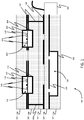
- FIG. 1 illustrates a superconducting device 100 according to one embodiment.
- the superconducting device comprises a plurality of substrates 101-105 that are bonded together in any suitable way.
- two substrates that have been covered, at least partially, with a metal material may be bonded together using cold welding, thermocompression bonding, thermosonic bonding, eutectic bonding or solder reflow.
- Any suitable number of substrates may be bonded together to form superconducting device 100.
- the embodiment illustrated in FIG. 1 shows five separate substrates 101-105, but embodiments are not so limited. For example, some embodiments may bond only two substrates together.
- substrate 101 and substrate 102 together form a bus layer, which is described in more detail in connection with FIGs. 3-4 below.
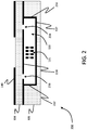
- Substrate 104 and substrate 105 together form a cavity memory layer, which is described in more detail below in connection with FIG. 2 .
- Substrate 103 is used as an interconnection layer used to interconnect various components within the superconducting device 100.
- the interconnection layer comprises at least one wiring layer formed from a superconducting material disposed on and/or within the substrate 103 in a pattern that is configured to interconnect different components of the superconducting device 100.
- the substrates 101-105 may comprise any suitable material.
- the material may include any material with a crystalline structure.
- silicon or germanium may be used.
- the substrate material may be insignificant as what controls the behavior of the superconducting device is the superconducting material that coats various portions of the substrate and the troughs that are created within the substrate to form enclosures.
- the substrates 101-105 may be of any suitable dimensions.
- the substrates 101-105 may have a thickness ranging from 300 ⁇ m to 500 ⁇ m.
- the superconducting layers of the superconducting device 100 may be formed in any suitable way.
- the surface of the substrate is covered with a superconducting material.
- one or more channels and/or troughs may be formed in the substrate that are subsequently covered, at least in part, with a superconducting material.
- Any suitable thickness of superconducting layer may be used.
- a superconducting layer of superconducting device 100 may have a thickness ranging from 1 ⁇ m to 10 ⁇ m.
- any suitable superconducting material may be used.
- the superconducting material may include aluminum, niobium, indium, rhenium, tantalum, titanium nitride, and/or niobium nitride.
- superconducting device 100 may communicate to external components via a planar-to-coaxial transition component 150 or any other suitable electronic connection, as known is in the art.
- FIG. 1 illustrates a single cross-section of the device showing three separate enclosures 110, 120 and 130.
- additional enclosures may be coupled to the enclosures 110, 120 and 130 through the wiring layer 140, the vias 142 and 144, and/or additional wiring layers and vias not illustrated.
- the wiring on a given layer or vias between layers may be separately enclosed by additional superconducting layers (not shown) realized by the same, or different, methods.
- a cavity memory layer may be formed from substrate 104 and 105.
- a trough is formed in the substrate 105 and covered, at least in part, with a superconducting layer 132. At least a portion of substrate 104 is also covered in a superconducting layer 134.
- the trough may be any suitable shape or size. For example, the trough may extend from a surface of the substrate by about 300 ⁇ m.
- the substrates are then positioned such that when connected together, a three-dimensional cavity resonator 130 is formed.
- FIG. 2 illustrates an embodiment 200 of a cavity memory layer in more detail.
- the three-dimensional cavity resonator130 includes at least a first surface 232 and a second surface 234 that are opposed to one another.
- the two surfaces are parallel to one other.
- the first surface 232 and the second surface 234 may both form a non-perpendicular angle with the superconducting layer 134 associated with substrate 104.
- every surface of the three-dimensional cavity resonator 130 is covered, at least in part, with a superconducting material.
- each surface of the three-dimensional cavity is covered in its entirety except for two apertures 236 and 238 formed in the superconducting layer 134.
- the apertures 236 and 238 may be used to couple electromagnetic radiation into the three-dimensional cavity resonator 130 from the wiring layer 140. Other methods of coupling to the cavity, which would be known by those skilled in the art, may also be employed.
- the geometry of the three-dimensional cavity resonator 130 determines which frequencies of electromagnetic radiation will be resonant with the cavity.
- the three-dimensional cavity resonator 130 may be configured to resonate at microwave frequencies.
- the three-dimensional cavity resonator 130 may be configured to resonate at at least one frequency ranging between 1 GHz and 20 GHz.
- the three-dimensional cavity 130 may be configured to resonate at at least one frequency ranging between 5 GHz and 9 GHz.
- the superconducting device 200 may include one or more superconducting qubits 131 disposed within the three-dimensional cavity resonator 130. Any suitable superconducting qubit may be used.
- each of the superconducting qubits 131 may be a transmon qubit or a fluxonium qubit.
- Each of the superconducting qubits 131 may comprise a Josephson junction disposed between two superconducting portions that act as a dipole antenna.
- the superconducting qubits 131 are oriented vertically such that the axis of each superconducting qubit (as determined by the orientation of the dipole antenna) is perpendicular to the superconducting layer 134 used to form the apertures 236 and 238, and the qubits thereby couple to the electromagnetic fields of the resonant cavity.
- the three-dimensional cavity resonator 130 does not contain a superconducting qubit, but is instead coupled to a superconducting qubit through wiring layer 140.
- an external superconducting qubit (not shown) may transfer quantum information to the three-dimensional cavity resonator 130, which may act as a memory for the quantum information.
- Quantum information may be stored in the three-dimensional cavity resonator 130in any suitable way.
- the energy eigenstates of the electromagnetic field may be used as the computational basis for encoding quantum information.
- different coherent states and/or superpositions of coherent state (sometimes called "cat states") may be used as the computational basis.
- Embodiments are not limited to any particular technique for encoding the quantum information in the three-dimensional cavity resonator 130.
- the bus layer includes enclosure 110 and enclosure 120, which are configured to be electromagnetic shields.
- Electromagnetic shield 110 includes a plurality of qubits 116 formed on and/or in a support layer 118 that is suspended within the electromagnetic shield 110.
- Electromagnetic shield 110 includes a superconducting layer 112 and a superconducting layer 114 for enclosing the qubits 116, thereby shielding the qubits 116 from external electromagnetic noise and preventing unwanted electromagnetic radiation from entering the enclosure.
- the electromagnetic shield 110 also prevents electromagnetic radiation from within the enclosure from leaking to the external environment.
- electromagnetic shield 120 includes a plurality of qubits 126 formed on and/or in a support layer 128 that is suspended within the cavity 120.
- Electromagnetic shield 120 includes a superconducting layer 122 and a superconducting layer 124 for enclosing the qubits 126, thereby shielding the qubits 126 from external electromagnetic noise and preventing unwanted electromagnetic radiation or cross-coupling to other elements of the device.
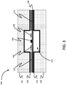
- FIG. 3 illustrates a more detailed cross-sectional view 300 of electromagnetic shield 110 according to some embodiments.
- Substrate 102 includes a trough from which the electromagnetic shield 110 is formed. At least a portion of the trough is covered with a superconducting layer 114. The superconducting layer 114 may also cover portions of the substrate 102 that are part of the trough.
- a plurality of qubits 116 are formed in and/or on a support layer 118.
- the support layer is a dielectric membrane suspended across the trough in substrate 102. Any suitable material may be used to form the support layer.
- the support layer may comprise silicon, silicon oxide, or silicon nitride.
- the plurality of qubits 116 may be any suitable superconducting qubit, such as a transmon qubit or a fluxonium qubit. Each individual qubit of the plurality of qubits 116 may be individually controlled and/or detected using feed lines 312, which are formed in and/or on the support layer 118.
- a stripline resonator 310 is disposed between a first plurality of qubits and a second plurality of qubits. In some embodiments, the stripline resonator 310 may be approximately 20 ⁇ m wide.
- the feed lines 312 and the stripline resonator 310 may be formed from any suitable superconducting material.
- Substrate 101 also includes a trough that has approximately the same dimensions and the trough in substrate 102. At least a portion of the trough in substrate 101 is covered with a superconducting layer 112. Substrate 101 is disposed near substrate 102 such that a gap exists between feedline 312 and superconducting layer 112. In some embodiments, the gap may be approximately 10 ⁇ m. Substrate 101 and substrate 102 may be in contact with each other at a location away from electromagnetic shield 110 such that they may be bonded together. By enclosing the stripline resonator 310 and the plurality of qubits 116 in an electromagnetic shield, the enclosed components are isolated from external electromagnetic noise, and decoherence due to unwanted electromagnetic radiation and cross-couplings are prevented.
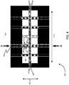
- FIG. 4 illustrates a top view 400 of the support layer 118 and the components included thereon.
- the arrows indicating "A" illustrate a plane representing the location of the cross-section view 300 of FIG. 3 .
- Membrane 118 includes a plurality of superconducting qubits 116.
- each superconducting qubit is a superconducting qubit, such as a transmon qubit or a fluxonium qubit.
- FIG. 4 illustrates transmon qubits 116 comprising a Josephson junction 412 between a first superconducting portion 414 and a second superconducting portion 416.
- Each qubit 116 may be individually controlled and/or read-out using drive feed lines 314.
- a large portion of the surface of the support layer 118 is covered with a superconducting layer as the ground plane for the stripline resonator 430.
- the stripline resonator 430 is driven via feedlines 420. There is a gap between the feedlines 420 and the stripline resonator such that the two components are weakly, capacitively coupled.
- Superconducting devices may be manufactured in any suitable way.
- microelectronic fabrication techniques may be used.
- the substrates may be formed with troughs and channels as desired using three-dimensional printing techniques and the superconducting layers may be formed using, for example, electroplating techniques.
- Some methods may create enclosures by forming a trough in a single substrate, as illustrate in FIG. 2 .
- enclosures may be created by forming a first trough in a first substrate and a second trough in a second substrate and placing the two substrates together with the two troughs adjacent to one another. Methods for forming superconducting devices according to some examples are described below with reference to FIGs. 5-10 .
- FIG. 5 illustrates a cross-sectional view of a plurality of acts of a method for constructing a superconducting device, methods not forming part of the invention .
- a flowchart of the acts of the method 700 is shown in FIG. 7 .
- a first trough is formed in a first substrate.
- the trough may be formed in any suitable way.
- the substrate and trough may be printed using three-dimensional printing techniques. Alternatively , microelectronic fabrication techniques may be used. Details of one such example is now described in connection with FIG. 5 , FIG. 6 and FIG. 8 .
- FIG. 5A illustrates a first substrate 500 being provided.
- the substrate may be formed from a material with a crystalline structure.
- the substrate may comprise silicon or germanium.
- the substrate 500 may be of any suitable thickness. In the illustrated examples , the substrate is approximately 500 ⁇ m thick.
- a silicon nitride layer 502 is deposited on a first surface of the substrate 500 (see FIG. 5B ). While silicon nitride is used in the illustrative example of FIG. 5 , any suitable material that may act as a mask may be used.
- a photoresist layer 504 is deposited on top of the silicon nitride layer 502 (see FIG. 5C ).
- the photoresist layer 504 is formed in a pattern based on the dimensions of the trough being formed in the substrate 500. Accordingly, the photoresist layer is absent from the region above where the trough will be formed in the substrate in the subsequent acts.
- the photoresist layer 504 may be formed such that an area of the silicon nitride layer 502 with dimensions 18 mm by 38 mm is left exposed.
- the exposed portion of the silicon nitride layer 502 is removed (see FIG. 5D ). This may be achieved in any suitable way.
- the silicon nitride layer 502 is etched using an etchant that removes the silicon nitride layer, but does not remove the photoresist.
- RIE reactive ion etching
- the act of RIE may use, for example, CHF 3 /O 2 as an etchant.
- the photoresist layer 504 is then removed at act 808.
- the resulting structure is the substrate 500 partially covered with the silicon nitride layer 502 which will act as a mask for defining dimensions of the trough (see FIG. 5E ).
- the exposed portion of the substrate 500 is etched to form a trough 506. Any suitable etching may be performed.
- the substrate 500 may be etched such that opposing surfaces of the resulting trough 506 are parallel to one another.
- the trough is etched using an anisotropic wet etch using 30% KOH at 85°C. The details of the anisotropic etch is shown in more detail in FIG. 6 .
- FIG. 6 illustrates the trough 506 resulting from an anisotropic wet etch. Because of the crystalline structure of the silicon substrate 500, the (100) plane 612 and the (111) 614 plane for a 54.7° angle as a result of the etching act. In some examples, the anisotropic wet etch results in surfaces 612 and 614 that are atomically smooth. Thus, when covered in a superconducting layer the surface of the resulting enclosure will be substantially free from defects. If the enclosure is configured for use as a three-dimensional cavity resonator, the smooth surfaces result in a high Q factor cavity.
- the silicon nitride layer is removed resulting in the substrate 500 including the trough 506 (see FIG. 5G ). While FIG. 8 illustrated one example of a method for creating a trough in a substrate, any suitable method may be used. For example, laser machining or three-dimensional printing may be used to form a substrate with a trough.
- the method 700 continues at act 704, where at least a portion of the first substrate is covered with a superconducting material .
- all the surfaces of the trough in the substrate may be covered.
- only portions of the surfaces may be covered. In this way, for example, apertures may be formed.
- portions of the substrate outside of the region associated with the trough may also be covered with a superconducting layer.
- the superconducting layer may be formed in any suitable way.
- FIGs. 5H-I illustrate one particular method for forming a superconducting layer that covers at least a portion of the substrate.
- FIG. 5H illustrates a thin seed layer 508 is deposited over the surface of the substrate 500. This may be done in any suitable way.
- copper is deposited via evaporation techniques to form the seed layer 508. Any suitable thickness of seed layer may be used.
- the seed layer 508 may be approximately 200 nm thick. While copper is used as an example material for the seed layer 508, any suitable material may be used.
- FIG. 5I illustrates a superconducting layer 510 formed on the seed layer 508.
- a superconducting material may be electroplated onto the seed layer.
- the superconducting layer 510 may be formed with any suitable thickness.
- the superconducting layer 510 may be approximately 10 ⁇ m thick. Any suitable superconducting material may be used.
- the superconducting layer may comprise aluminum, niobium, indium, rhenium, tantalum, titanium nitride, or niobium nitride.
- a second trough is formed in a second substrate.
- the act of forming the second trough may be achieved using the same techniques described in connection with act 702, FIG. 5 and FIG. 8 .
- the formation of the second trough is optional.
- An enclosure may be formed from a single trough in a first substrate without forming a second trough in a second substrate.
- At act 710 at least one superconducting qubit is formed on a support layer.
- the support layer may be any suitable dielectric membrane.
- the support layer may comprise silicon, silicon oxide, or silicon nitride.
- act 710 may be omitted as superconducting devices may be formed without a superconducting qubit being enclosed in an enclosure.
- the first substrate and the second substrate are bonded together to form an enclosure.
- the two troughs are positioned adjacent to one another such that the enclosure is formed from both troughs together.
- the support layer is suspended across the first trough prior to bonding the two substrates together. Accordingly, the at least one qubit in and/or on the support layer is disposed within the enclosure.
- the method 700 may also include additional optional acts shown in FIG. 9 and FIG. 10 .
- the result of performing method 700 may be the formation of enclosure 110 in the bus layer of FIG. 1 .
- FIG. 9 illustrates additional acts for forming the wiring layer 140 and the memory layer enclosure 130.
- FIG. 10 illustrates additional acts for forming the second enclosure 120 in the bus layer.
- FIG. 9 illustrates additional acts 900 for forming the wiring layer and the memory layer.
- the additional acts may be performed after the method 700. In other examples, the additional acts may be performed before the method 700 or simultaneously with method 700.
- At act 902 at least one channel is formed in wiring layer substrate 103 (see FIG. 1 ).
- the at least one channel may be formed, for example, using the same process used to create the trough in act 702.
- At act 904 at least a portion of the at least one channel is covered with superconducting material. This may be achieved using the same process used above in connection with act 704.
- the channel may be completely filled with superconducting material.
- the one or more of the surfaces of the at least one channel may be covered with the superconducting material.
- the wiring substrate 103 is bonded to substrate 102.
- the substrates may be bonded in any suitable way, as discussed above.
- a trough is formed in substrate 105 using, for example, the same process used to create the trough in act 702.
- At act 910 at least a portion of substrate 105 is covered with a superconducting material. This may be achieved using the same process used above in connection with act 704. In some examples, each surface of the through is completely covered with superconducting material.
- the superconducting material is formed in a layer that may be any suitable thickness. In some examples , the superconducting layer may be approximately 1 ⁇ m thick. In other examples , the superconducting layer may be approximately 10 ⁇ m thick.
- At act 912 at least a portion of substrate 104 is covered with a superconducting material. This may be achieved using the same process used above in connection with act 704. Certain portions of a surface of substrate 104 may be left exposed. For example, the area corresponding to apertures 236 and 238 in FIG. 2 may not be covered with superconducting material.
- substrate 104 is bonded to substrate 105 such that the trough forms a three-dimensional cavity resonator.
- the substrates may be bonded in any suitable way, as discussed above.
- the memory layer is bonded to the wiring layer.
- the substrates associated with the layers may be bonded in any suitable way, as discussed above.
- FIG. 10 illustrates additional acts for forming the second enclosure 120 in the bus layer.
- a trough associated with enclosure 120 is formed in the substrate 101 using, for example, the same process used to create the trough in act 702.
- the trough associate with enclosure 120 may be formed simultaneously with the trough associated with enclosure 110.
- a trough associated with enclosure 120 is formed in the substrate 102 using, for example, the same process used to create the trough in act 702.
- the trough associate with enclosure 120 may be formed simultaneously with the trough associated with enclosure 110.
- At act 1006 at least a portion of substrate 102 may be covered with a support layer which is suspended over the trough associated with enclosure 120.
- This support layer may be formed in the same way as the support layer associated with enclosure 110.
- At act 1008 at least one qubit is formed on the support layer. This at least one qubit may be formed in the same way as the support layer associated with enclosure 110.
- the technology described may be embodied as a method, of which at least one example has been provided, the method not forming part of the invention.
- the terms “about,” “approximately,” and “substantially” may be used to refer to a value, and are intended to encompass the referenced value plus and minus acceptable variations.
- the amount of variation could be less than 5% in some embodiments, less than 10% in some embodiments, and yet less than 20% in some embodiments.
- the amount of variation could be a factor of two. For example, if an apparatus functions properly for a value ranging from 20 to 350, "approximately 80" may encompass values between 40 and 160.
- a reference to "A and/or B", when used in conjunction with open-ended language such as “comprising” can refer, in one embodiment, to A only (optionally including elements other than B); in another embodiment, to B only (optionally including elements other than A); in yet another embodiment, to both A and B (optionally including other elements); etc.
- the phrase "at least one,” in reference to a list of one or more elements, should be understood to mean at least one element selected from any one or more of the elements in the list of elements, but not necessarily including at least one of each and every element specifically listed within the list of elements and not excluding any combinations of elements in the list of elements.
- This definition also allows that elements may optionally be present other than the elements specifically identified within the list of elements to which the phrase "at least one" refers, whether related or unrelated to those elements specifically identified.
- At least one of A and B can refer, in one embodiment, to at least one, optionally including more than one, A, with no B present (and optionally including elements other than B); in another embodiment, to at least one, optionally including more than one, B, with no A present (and optionally including elements other than A); in yet another embodiment, to at least one, optionally including more than one, A, and at least one, optionally including more than one, B (and optionally including other elements); etc.
Claims (22)
- Eine Vorrichtung, die Folgendes aufweist:eine Vielzahl von Substraten, die eine oder mehrere Mulden umfassen, wobei die Vielzahl von Substraten so angeordnet ist, dass die eine oder mehreren Mulden mindestens ein Gehäuse (130) bilden; undmindestens eine supraleitende Schicht (132, 134), die mindestens einen Teil des mindestens einen Gehäuses (130) bedeckt,wobei das mindestens eine Gehäuse (130) so konfiguriert ist, dass es mindestens einen dreidimensionalen Hohlraumresonator bildet, so dass elektromagnetische Strahlung mit einer oder mehreren Frequenzen innerhalb des mindestens einen dreidimensionalen Hohlraumresonators in Resonanz tritt.
- Vorrichtung nach Anspruch 1, wobei ein Q-Faktor des mindestens einen dreidimensionalen Hohlraumresonators (130) größer als zehn Millionen ist.
- Vorrichtung nach Anspruch 1 oder 2, wobei der mindestens eine dreidimensionale Hohlraumresonator (130) einen ersten dreidimensionalen Hohlraumresonator und einen zweiten dreidimensionalen Hohlraumresonator aufweist, wobei ein Q-Faktor des ersten dreidimensionalen Hohlraumresonators größer ist als ein Q-Faktor des zweiten dreidimensionalen Hohlraumresonators.
- Die Vorrichtung nach einem der Ansprüche 1 bis 3, die ferner Folgendes aufweist:
mindestens ein supraleitendes Qubit (131), das mit dem mindestens einen dreidimensionalen Hohlraumresonator (130) gekoppelt ist. - Vorrichtung nach Anspruch 4, wobei das mindestens eine supraleitende Qubit (131) ein Transmon-Qubit oder ein Fluxonium-Qubit ist.
- Vorrichtung nach Anspruch 4 oder 5, die ferner Folgendes aufweist:
eine supraleitende Verdrahtungsschicht (140), die auf und/oder in einem ersten Substrat der Vielzahl von Substraten angeordnet ist, wobei die supraleitende Verdrahtungsschicht (140) so konfiguriert ist, dass sie das mindestens eine supraleitende Qubit mit dem mindestens einen dreidimensionalen Hohlraumresonator (130) koppelt. - Vorrichtung nach Anspruch 6, die ferner mindestens eines der folgenden Elemente aufweist:eine Öffnung in der mindestens einen supraleitenden Schicht (132, 134), die so konfiguriert ist, dass sie die supraleitende Verdrahtungsschicht (140) mit dem mindestens einen dreidimensionalen Hohlraumresonator (130) koppelt; undeinen Durchgang (142), der die supraleitende Verdrahtungsschicht mit mindestens einer supraleitenden Komponente eines zweiten Substrats aus der Vielzahl von Substraten verbindet.
- Vorrichtung nach einem der Ansprüche 4 bis 7, wobei das mindestens eine supraleitende Qubit (131) innerhalb des mindestens einen dreidimensionalen Hohlraumresonators (130) so angeordnet ist, dass das mindestens eine supraleitende Qubit (131) so konfiguriert ist, dass es über elektromagnetische Strahlung an den mindestens einen dreidimensionalen Hohlraumresonator (130) koppelt.
- Vorrichtung nach einem der Ansprüche 1 bis 8, wobei die eine oder mehreren Frequenzen mindestens eine Mikrowellenfrequenz aufweisen.
- Die Vorrichtung nach einem der Ansprüche 1 bis 9, wobei:die Mehrzahl von Substraten ein erstes Substrat und ein zweites Substrat aufweist;das erste Substrat eine erste Mulde der einen oder mehreren Mulden umfasst;die mindestens eine supraleitende Schicht Folgendes aufweist:eine erste supraleitende Schicht (132), die mindestens einen Teil der ersten Mulde bedeckt; undeine zweite supraleitende Schicht (134), die mindestens einen Teil einer Oberfläche des zweiten Substrats bedeckt; unddas erste Substrat und das zweite Substrat so angeordnet sind, dass die erste supraleitende Schicht und die zweite supraleitende Schicht in direktem Kontakt sind und die erste Mulde den mindestens einen dreidimensionalen Hohlraumresonator (130) bildet.
- Eine Vorrichtung, die Folgendes aufweist:eine Vielzahl von Substraten, die eine oder mehrere Mulden aufweisen, wobei die Vielzahl von Substraten so angeordnet ist, dass die eine oder mehreren Mulden mindestens ein Gehäuse (110, 120) bilden; undmindestens eine supraleitende Schicht (112, 114, 122, 124), die mindestens einen Teil des mindestens einen Gehäuses (110, 120) bedeckt,wobei das mindestens eine Gehäuse (110, 120) so konfiguriert ist, dass es mindestens einen Hohlraum bildet,und wobei:das mindestens eine Gehäuse (110, 120) so konfiguriert ist, dass es mindestens eine elektromagnetische Abschirmung bildet, so dass externe elektromagnetische Strahlung daran gehindert wird, in das mindestens eine Gehäuse einzudringen, wobei die Vorrichtung ferner Folgendes aufweistmindestens eine supraleitende Komponente (116, 126), die innerhalb der mindestens einen elektromagnetischen Abschirmung angeordnet ist.
- Vorrichtung nach Anspruch 11, wobei die mindestens eine supraleitende Komponente (116, 126) mindestens eine der folgenden Komponenten aufweist:eine supraleitende Schaltung; undein Qubit.
- Vorrichtung nach Anspruch 12, wobei die mindestens eine supraleitende Komponente (110, 120) mindestens ein Qubit und mindestens einen Streifenleitungsresonator aufweist.
- Die Vorrichtung nach Anspruch 13, wobei:die Mehrzahl von Substraten ein erstes Substrat und ein zweites Substrat aufweist;das erste Substrat eine erste Mulde der einen oder mehreren Mulden aufweist;das zweite Substrat eine zweite Mulde der einen oder mehreren Mulden umfasst;die mindestens eine supraleitende Schicht (112, 114, 122, 124) Folgendes aufweist:eine erste supraleitende Schicht, die mindestens einen Teil der ersten Mulde bedeckt; undeine zweite supraleitende Schicht, die mindestens einen Teil der zweiten Mulde bedeckt;das erste Substrat und das zweite Substrat so angeordnet sind, dass die erste Mulde und die zweite Mulde das mindestens eine Gehäuse (110, 120) bilden; undder mindestens eine Streifenleitungsresonator innerhalb der mindestens einen elektromagnetischen Abschirmung angeordnet ist.
- Die Vorrichtung nach Anspruch 14, die ferner Folgendes aufweist
mindestens eine Trägerschicht (118), die innerhalb der mindestens einen elektromagnetischen Abschirmung getragen wird, wobei der mindestens eine Streifenleitungsresonator auf und/oder in der mindestens einen Trägerschicht (118) angeordnet ist. - Vorrichtung nach Anspruch 15, wobei die mindestens eine Trägerschicht (118) mindestens ein Material aufweist, das aus der Gruppe ausgewählt ist, die aus Silizium, Siliziumoxid und Siliziumnitrid besteht.
- Vorrichtung nach einem der Ansprüche 13 bis 16, wobei die mindestens eine elektromagnetische Abschirmung so konfiguriert ist, dass sie Teil einer mit dem mindestens einen Streifenleitungsresonator verbundenen Schaltung ist.
- Vorrichtung nach einem der Ansprüche 1 bis 17, wobei die mehreren Substrate ein Material mit einer kristallinen Struktur aufweisen.
- Vorrichtung nach Anspruch 18, wobei das Material Silizium ist.
- Vorrichtung nach einem der Ansprüche 1 bis 19, wobei die eine oder die mehreren Mulden eine erste Mulde mit einer ersten Durchgangsfläche umfassen, die einer zweiten Durchgangsfläche gegenüberliegt, wobei die erste Durchgangsfläche nicht parallel zu der zweiten Durchgangsfläche ist.
- Vorrichtung nach einem der Ansprüche 1 bis 20, wobei mindestens eine Oberfläche des einen oder der mehreren Mulden atomar glatt ist.
- Vorrichtung nach einem der Ansprüche 1 bis 21, wobei das mindestens eine Gehäuse (110, 120, 130) auf einen Druck unter Atmosphärendruck evakuiert ist.
Applications Claiming Priority (2)
| Application Number | Priority Date | Filing Date | Title |
|---|---|---|---|
| US201361754298P | 2013-01-18 | 2013-01-18 | |
| PCT/US2014/012073 WO2014163728A2 (en) | 2013-01-18 | 2014-01-17 | Superconducting device with at least one enclosure |
Publications (3)
| Publication Number | Publication Date |
|---|---|
| EP2946413A2 EP2946413A2 (de) | 2015-11-25 |
| EP2946413A4 EP2946413A4 (de) | 2016-09-14 |
| EP2946413B1 true EP2946413B1 (de) | 2022-01-05 |
Family
ID=51659290
Family Applications (1)
| Application Number | Title | Priority Date | Filing Date |
|---|---|---|---|
| EP14778477.1A Active EP2946413B1 (de) | 2013-01-18 | 2014-01-17 | Supraleitende vorrichtung mit mindestens einem gehäuse |
Country Status (8)
| Country | Link |
|---|---|
| US (1) | US10424711B2 (de) |
| EP (1) | EP2946413B1 (de) |
| JP (2) | JP6461009B2 (de) |
| KR (1) | KR102178986B1 (de) |
| CA (1) | CA2898598C (de) |
| HK (1) | HK1218022A1 (de) |
| SG (1) | SG11201505616YA (de) |
| WO (1) | WO2014163728A2 (de) |
Families Citing this family (27)
| Publication number | Priority date | Publication date | Assignee | Title |
|---|---|---|---|---|
| SG11201505617UA (en) | 2013-01-18 | 2015-09-29 | Univ Yale | Methods for making a superconducting device with at least one enclosure |
| US10496934B2 (en) | 2014-02-28 | 2019-12-03 | Rigetti & Co, Inc. | Housing qubit devices in an electromagnetic waveguide system |
| KR20170134399A (ko) | 2015-02-27 | 2017-12-06 | 예일 유니버시티 | 평면 큐비트를 비-평면 공진기에 결합하기 위한 기술 및 관련 시스템 및 방법 |
| US9836699B1 (en) | 2015-04-27 | 2017-12-05 | Rigetti & Co. | Microwave integrated quantum circuits with interposer |
| US10068181B1 (en) | 2015-04-27 | 2018-09-04 | Rigetti & Co, Inc. | Microwave integrated quantum circuits with cap wafer and methods for making the same |
| CN117915758A (zh) | 2016-09-13 | 2024-04-19 | 谷歌有限责任公司 | 堆叠量子器件和用于制造堆叠量子器件的方法 |
| WO2018063204A1 (en) * | 2016-09-29 | 2018-04-05 | Intel Corporation | Quantum computing assemblies |
| US10176432B2 (en) * | 2017-03-07 | 2019-01-08 | International Business Machines Corporation | Weakly tunable qubit based on two coupled disparate transmons |
| KR102217205B1 (ko) * | 2017-03-13 | 2021-02-18 | 구글 엘엘씨 | 적층된 양자 컴퓨팅 디바이스 내의 집적 회로 소자 |
| US11276727B1 (en) | 2017-06-19 | 2022-03-15 | Rigetti & Co, Llc | Superconducting vias for routing electrical signals through substrates and their methods of manufacture |
| US11121301B1 (en) * | 2017-06-19 | 2021-09-14 | Rigetti & Co, Inc. | Microwave integrated quantum circuits with cap wafers and their methods of manufacture |
| CA3074722C (en) * | 2017-09-13 | 2023-09-05 | Google Llc | Hybrid kinetic inductance devices for superconducting quantum computing |
| US10256206B2 (en) * | 2018-03-16 | 2019-04-09 | Intel Corporation | Qubit die attachment using preforms |
| US10243132B1 (en) | 2018-03-23 | 2019-03-26 | International Business Machines Corporation | Vertical josephson junction superconducting device |
| US10672971B2 (en) | 2018-03-23 | 2020-06-02 | International Business Machines Corporation | Vertical transmon qubit device with microstrip waveguides |
| US10256392B1 (en) | 2018-03-23 | 2019-04-09 | International Business Machines Corporation | Vertical transmon qubit device |
| US10497746B1 (en) | 2018-05-25 | 2019-12-03 | International Business Machines Corporation | Three-dimensional integration for qubits on crystalline dielectric |
| US10505096B1 (en) | 2018-05-25 | 2019-12-10 | International Business Machines Corporation | Three-dimensional integration for qubits on multiple height crystalline dielectric |
| TWI809224B (zh) * | 2018-11-22 | 2023-07-21 | 國立研究開發法人科學技術振興機構 | 非線性微波濾波器 |
| US11223355B2 (en) | 2018-12-12 | 2022-01-11 | Yale University | Inductively-shunted transmon qubit for superconducting circuits |
| JP6986788B2 (ja) * | 2019-10-02 | 2021-12-22 | 大輔 才田 | 量子回路システム |
| DE102020201688B3 (de) | 2020-02-11 | 2021-07-29 | Forschungszentrum Jülich GmbH | Schaltkreis mit gekoppelten Qubits mit unterschiedlich anharmonischem Energiespektrum |
| FR3114444B1 (fr) * | 2020-09-21 | 2022-09-30 | Commissariat Energie Atomique | Puce à routage bifonctionnel et procédé de fabrication associé |
| JPWO2022113889A1 (de) * | 2020-11-30 | 2022-06-02 | ||
| US11664801B1 (en) | 2021-12-08 | 2023-05-30 | International Business Machines Corporation | Multi-qubit architectures with mode-selective charge coupling between novel fluxonium-molecule qubits |
| CN115697029B (zh) * | 2022-12-30 | 2023-06-20 | 量子科技长三角产业创新中心 | 一种超导量子芯片及其制备方法 |
| CN115915907B (zh) * | 2023-01-05 | 2023-09-12 | 量子科技长三角产业创新中心 | 一种超导量子芯片制备方法及超导量子芯片 |
Family Cites Families (88)
| Publication number | Priority date | Publication date | Assignee | Title |
|---|---|---|---|---|
| US3723755A (en) | 1970-10-12 | 1973-03-27 | A Morse | Parametric amplifier |
| US4403189A (en) | 1980-08-25 | 1983-09-06 | S.H.E. Corporation | Superconducting quantum interference device having thin film Josephson junctions |
| US4344052A (en) | 1980-09-29 | 1982-08-10 | International Business Machines Corporation | Distributed array of Josephson devices with coherence |
| US4585999A (en) | 1984-04-27 | 1986-04-29 | The United States Of America As Represented By The United States Department Of Energy | Radiofrequency amplifier based on a dc superconducting quantum interference device |
| JPS6182449A (ja) * | 1984-09-28 | 1986-04-26 | Mitsubishi Electric Corp | プラスチツクモ−ルド型半導体装置 |
| US4780724A (en) | 1986-04-18 | 1988-10-25 | General Electric Company | Antenna with integral tuning element |
| US4924234A (en) | 1987-03-26 | 1990-05-08 | Hughes Aircraft Company | Plural level beam-forming network |
| GB2219434A (en) | 1988-06-06 | 1989-12-06 | Philips Nv | A method of forming a contact in a semiconductor device |
| JPH02194638A (ja) * | 1989-01-24 | 1990-08-01 | Fujitsu Ltd | 半導体装置 |
| US5105166A (en) | 1989-11-30 | 1992-04-14 | Raytheon Company | Symmetric bi-directional amplifier |
| US5075655A (en) * | 1989-12-01 | 1991-12-24 | The United States Of America As Represented By The Secretary Of The Navy | Ultra-low-loss strip-type transmission lines, formed of bonded substrate layers |
| US5326986A (en) | 1991-03-05 | 1994-07-05 | University Of Houston - University Park | Parallel N-junction superconducting interferometer with enhanced flux-to-voltage transfer function |
| US5186379A (en) | 1991-06-17 | 1993-02-16 | Hughes Aircraft Company | Indium alloy cold weld bumps |
| US5254950A (en) | 1991-09-13 | 1993-10-19 | The Regents, University Of California | DC superconducting quantum interference device usable in nuclear quadrupole resonance and zero field nuclear magnetic spectrometers |
| US5296457A (en) * | 1992-03-23 | 1994-03-22 | The Regents Of The University Of California | Clamshell microwave cavities having a superconductive coating |
| CA2132149C (en) | 1993-09-15 | 2003-11-11 | Graeme John Sloggett | Squid detector for tem prospecting |
| US5493719A (en) | 1994-07-01 | 1996-02-20 | The United States Of America As Represented By The Secretary Of The Air Force | Integrated superconductive heterodyne receiver |
| JP3421184B2 (ja) | 1995-12-19 | 2003-06-30 | 理化学研究所 | 波長可変レーザーにおける波長選択方法および波長可変レーザーにおける波長選択可能なレーザー発振装置 |
| RU2106717C1 (ru) | 1996-08-07 | 1998-03-10 | Научно-исследовательский институт измерительных систем | Способ анизотропного травления кристаллов кремния |
| US6578018B1 (en) | 1999-07-27 | 2003-06-10 | Yamaha Hatsudoki Kabushiki Kaisha | System and method for control using quantum soft computing |
| US6486756B2 (en) | 2000-03-27 | 2002-11-26 | Hitachi, Ltd. | Superconductor signal amplifier |
| US6627915B1 (en) | 2000-08-11 | 2003-09-30 | D-Wave Systems, Inc. | Shaped Josephson junction qubits |
| US20030027724A1 (en) | 2000-12-22 | 2003-02-06 | D-Wave Systems, Inc. | Phase shift device in superconductor logic |
| US6549059B1 (en) | 2001-02-23 | 2003-04-15 | Trw Inc. | Underdamped Josephson transmission line |
| US6934649B2 (en) | 2001-05-15 | 2005-08-23 | Synchro Kabushiki Kaisha | Waveform detection system and state-monitoring system |
| EP1262911A1 (de) | 2001-05-30 | 2002-12-04 | Hitachi Europe Limited | Quantenrechner |
| US6803599B2 (en) | 2001-06-01 | 2004-10-12 | D-Wave Systems, Inc. | Quantum processing system for a superconducting phase qubit |
| US6621374B2 (en) | 2001-07-19 | 2003-09-16 | Lockheed Martin Corporation | Splitter/combiner using artificial transmission lines, and paralleled amplifier using same |
| RU2212671C1 (ru) | 2001-10-11 | 2003-09-20 | Алексенко Андрей Геннадьевич | Туннельный нанодатчик механических колебаний и способ его изготовления |
| US6614047B2 (en) | 2001-12-17 | 2003-09-02 | D-Wave Systems, Inc. | Finger squid qubit device |
| US6908779B2 (en) | 2002-01-16 | 2005-06-21 | Matsushita Electric Industrial Co., Ltd. | Semiconductor device and method for manufacturing the same |
| US7307275B2 (en) | 2002-04-04 | 2007-12-11 | D-Wave Systems Inc. | Encoding and error suppression for superconducting quantum computers |
| US6911664B2 (en) | 2002-04-15 | 2005-06-28 | D-Wave Systems, Inc. | Extra-substrate control system |
| US6900454B2 (en) | 2002-04-20 | 2005-05-31 | D-Wave Systems, Inc. | Resonant controlled qubit system |
| FR2839389B1 (fr) | 2002-05-03 | 2005-08-05 | Commissariat Energie Atomique | Dispositif de bit quantique supraconducteur a jonctions josephson |
| US6943368B2 (en) | 2002-11-25 | 2005-09-13 | D-Wave Systems, Inc. | Quantum logic using three energy levels |
| US7364923B2 (en) | 2003-03-03 | 2008-04-29 | The Governing Council Of The University Of Toronto | Dressed qubits |
| WO2004084132A2 (en) | 2003-03-18 | 2004-09-30 | Magiq Technologies, Inc. | Universal quantum computing |
| CA2527911C (en) | 2003-06-13 | 2010-09-14 | Qest Quantenelektronische Systeme Tuebingen Gmbh Sitz Boeblingen | Superconducting quantum antenna |
| JP4113076B2 (ja) | 2003-08-28 | 2008-07-02 | 株式会社日立製作所 | 超電導半導体集積回路 |
| US6995404B2 (en) | 2003-10-22 | 2006-02-07 | The Johns Hopkins University | Techniques for quantum processing with photons and the zeno effect |
| US20050134377A1 (en) | 2003-12-23 | 2005-06-23 | Dent Paul W. | Doherty amplifier |
| US7418283B2 (en) | 2004-03-29 | 2008-08-26 | D-Wave Systems Inc. | Adiabatic quantum computation with superconducting qubits |
| US7225674B2 (en) | 2004-04-30 | 2007-06-05 | The Regents Of The University Of California | Self-stabilizing, floating microelectromechanical device |
| WO2006011451A1 (ja) | 2004-07-27 | 2006-02-02 | Japan Science And Technology Agency | ジョセフソン量子計算素子及びそれを用いた集積回路 |
| US7253654B2 (en) | 2004-11-08 | 2007-08-07 | D-Wave Systems Inc. | Superconducting qubits having a plurality of capacitive couplings |
| US7533068B2 (en) | 2004-12-23 | 2009-05-12 | D-Wave Systems, Inc. | Analog processor comprising quantum devices |
| US7375802B2 (en) | 2005-08-04 | 2008-05-20 | Lockheed Martin Corporation | Radar systems and methods using entangled quantum particles |
| US8164082B2 (en) | 2005-09-30 | 2012-04-24 | Wisconsin Alumni Research Foundation | Spin-bus for information transfer in quantum computing |
| US7836007B2 (en) | 2006-01-30 | 2010-11-16 | Hewlett-Packard Development Company, L.P. | Methods for preparing entangled quantum states |
| US7870087B2 (en) | 2006-11-02 | 2011-01-11 | D-Wave Systems Inc. | Processing relational database problems using analog processors |
| AU2007329156B2 (en) | 2006-12-05 | 2012-09-13 | D-Wave Systems Inc. | Systems, methods and apparatus for local programming of quantum processor elements |
| US7724020B2 (en) | 2007-12-13 | 2010-05-25 | Northrop Grumman Systems Corporation | Single flux quantum circuits |
| US7800395B2 (en) | 2007-05-02 | 2010-09-21 | D-Wave Systems Inc. | Systems, devices, and methods for controllably coupling qubits |
| US7899092B2 (en) | 2007-05-22 | 2011-03-01 | Magiq Technologies, Inc. | Fast quantum gates with ultrafast chirped pulses |
| US7859744B2 (en) | 2007-07-27 | 2010-12-28 | Magiq Technologies, Inc. | Tunable compact entangled-photon source and QKD system using same |
| US7498832B2 (en) | 2007-08-03 | 2009-03-03 | Northrop Grumman Systems Corporation | Arbitrary quantum operations with a common coupled resonator |
| US8149494B1 (en) | 2007-09-07 | 2012-04-03 | The United States Of America As Represented By The Secretary Of The Navy | Two-photon absorption switch having which-path exclusion and monolithic mach-zehnder interferometer |
| US20090074355A1 (en) | 2007-09-17 | 2009-03-19 | Beausoleil Raymond G | Photonically-coupled nanoparticle quantum systems and methods for fabricating the same |
| US7932515B2 (en) * | 2008-01-03 | 2011-04-26 | D-Wave Systems Inc. | Quantum processor |
| US8260145B2 (en) | 2008-03-12 | 2012-09-04 | Deepnarayan Gupta | Digital radio frequency tranceiver system and method |
| KR20100133994A (ko) | 2008-03-30 | 2010-12-22 | 힐스 인크. | 초전도 와이어 및 케이블, 초전도 와이어 및 케이블을 제조하기 위한 방법 |
| US7932514B2 (en) | 2008-05-23 | 2011-04-26 | International Business Machines Corporation | Microwave readout for flux-biased qubits |
| US7969178B2 (en) | 2008-05-29 | 2011-06-28 | Northrop Grumman Systems Corporation | Method and apparatus for controlling qubits with single flux quantum logic |
| WO2009152180A2 (en) | 2008-06-10 | 2009-12-17 | D-Wave Systems Inc. | Parameter learning system for solvers |
| US7724083B2 (en) | 2008-08-05 | 2010-05-25 | Northrop Grumman Systems Corporation | Method and apparatus for Josephson distributed output amplifier |
| JP5091813B2 (ja) | 2008-09-17 | 2012-12-05 | 株式会社東芝 | 量子ゲート方法および装置 |
| EP2659987A1 (de) | 2009-03-26 | 2013-11-06 | Norwegian University of Science and Technology (NTNU) | Akustische-Rückschicht für die Verwendung in einem Ultraschallwandler |
| US8456856B2 (en) | 2009-03-30 | 2013-06-04 | Megica Corporation | Integrated circuit chip using top post-passivation technology and bottom structure technology |
| EP2249173A1 (de) | 2009-05-08 | 2010-11-10 | Mbda Uk Limited | Radargerät mit Verstärkerduplexer |
| IT1398934B1 (it) | 2009-06-18 | 2013-03-28 | Edison Spa | Elemento superconduttivo e relativo procedimento di preparazione |
| FR2950877B1 (fr) * | 2009-10-07 | 2012-01-13 | Commissariat Energie Atomique | Structure a cavite comportant une interface de collage a base de materiau getter |
| US8600200B1 (en) | 2010-04-01 | 2013-12-03 | Sandia Corporation | Nano-optomechanical transducer |
| US8525619B1 (en) | 2010-05-28 | 2013-09-03 | Sandia Corporation | Lateral acoustic wave resonator comprising a suspended membrane of low damping resonator material |
| US8111083B1 (en) | 2010-12-01 | 2012-02-07 | Northrop Grumman Systems Corporation | Quantum processor |
| US8416109B2 (en) | 2010-12-16 | 2013-04-09 | Hypres, Inc. | Superconducting analog-to-digital converter with current amplified feedback |
| US9379303B2 (en) | 2011-06-14 | 2016-06-28 | Glocbalfoundries Inc. | Modular array of fixed-coupling quantum systems for quantum information processing |
| US8861619B2 (en) | 2011-08-16 | 2014-10-14 | Wisconsin Alumni Research Foundation | System and method for high-frequency amplifier |
| US8837544B2 (en) * | 2011-10-28 | 2014-09-16 | Hewlett-Packard Development Company, L.P. | Quantum optical device |
| US8841764B2 (en) | 2012-01-31 | 2014-09-23 | International Business Machines Corporation | Superconducting quantum circuit having a resonant cavity thermalized with metal components |
| US9601103B2 (en) | 2012-10-19 | 2017-03-21 | The Regents Of The University Of Michigan | Methods and devices for generating high-amplitude and high-frequency focused ultrasound with light-absorbing materials |
| SG11201505617UA (en) | 2013-01-18 | 2015-09-29 | Univ Yale | Methods for making a superconducting device with at least one enclosure |
| US9350460B2 (en) | 2013-04-23 | 2016-05-24 | Raytheon Bbn Technologies Corp. | System and method for quantum information transfer between optical photons and superconductive qubits |
| US10496934B2 (en) | 2014-02-28 | 2019-12-03 | Rigetti & Co, Inc. | Housing qubit devices in an electromagnetic waveguide system |
| KR102344884B1 (ko) | 2014-11-25 | 2021-12-29 | 삼성전자주식회사 | 멀티 큐빗 커플링 구조 |
| KR20170134399A (ko) | 2015-02-27 | 2017-12-06 | 예일 유니버시티 | 평면 큐비트를 비-평면 공진기에 결합하기 위한 기술 및 관련 시스템 및 방법 |
| US9836699B1 (en) | 2015-04-27 | 2017-12-05 | Rigetti & Co. | Microwave integrated quantum circuits with interposer |
| US9503063B1 (en) | 2015-09-16 | 2016-11-22 | International Business Machines Corporation | Mechanically tunable superconducting qubit |
-
2014
- 2014-01-17 JP JP2015553853A patent/JP6461009B2/ja active Active
- 2014-01-17 EP EP14778477.1A patent/EP2946413B1/de active Active
- 2014-01-17 CA CA2898598A patent/CA2898598C/en active Active
- 2014-01-17 US US14/761,912 patent/US10424711B2/en active Active
- 2014-01-17 SG SG11201505616YA patent/SG11201505616YA/en unknown
- 2014-01-17 WO PCT/US2014/012073 patent/WO2014163728A2/en active Application Filing
- 2014-01-17 KR KR1020157022221A patent/KR102178986B1/ko active IP Right Grant
-
2016
- 2016-05-23 HK HK16105868.0A patent/HK1218022A1/zh unknown
-
2018
- 2018-11-02 JP JP2018207501A patent/JP6744379B2/ja active Active
Also Published As
| Publication number | Publication date |
|---|---|
| CA2898598C (en) | 2023-01-03 |
| EP2946413A4 (de) | 2016-09-14 |
| KR102178986B1 (ko) | 2020-11-18 |
| EP2946413A2 (de) | 2015-11-25 |
| US20150357550A1 (en) | 2015-12-10 |
| WO2014163728A2 (en) | 2014-10-09 |
| JP6461009B2 (ja) | 2019-01-30 |
| KR20150127045A (ko) | 2015-11-16 |
| SG11201505616YA (en) | 2015-09-29 |
| HK1218022A1 (zh) | 2017-01-27 |
| JP6744379B2 (ja) | 2020-08-19 |
| JP2016509800A (ja) | 2016-03-31 |
| JP2019050399A (ja) | 2019-03-28 |
| WO2014163728A3 (en) | 2014-12-31 |
| CA2898598A1 (en) | 2014-10-09 |
| US10424711B2 (en) | 2019-09-24 |
Similar Documents
| Publication | Publication Date | Title |
|---|---|---|
| EP2946413B1 (de) | Supraleitende vorrichtung mit mindestens einem gehäuse | |
| CA2898608C (en) | Methods for making a superconducting device with at least one enclosure | |
| EP3580702B1 (de) | Integration von schaltungselementen in eine gestapelte quanten-computing-vorrichtung | |
| US10468740B2 (en) | Techniques for coupling planar qubits to non-planar resonators and related systems and methods | |
| WO2019032115A1 (en) | QUANTIC BIT DEVICES WITH JOSEPHSON JUNCTION CONNECTED BELOW SUPPORT CIRCUITS | |
| CN112313796B (zh) | 载体芯片、制造载体芯片的方法和量子计算器件 | |
| CN109891591A (zh) | 减少堆叠量子器件中的损耗 |
Legal Events
| Date | Code | Title | Description |
|---|---|---|---|
| PUAI | Public reference made under article 153(3) epc to a published international application that has entered the european phase |
Free format text: ORIGINAL CODE: 0009012 |
|
| 17P | Request for examination filed |
Effective date: 20150807 |
|
| AK | Designated contracting states |
Kind code of ref document: A2 Designated state(s): AL AT BE BG CH CY CZ DE DK EE ES FI FR GB GR HR HU IE IS IT LI LT LU LV MC MK MT NL NO PL PT RO RS SE SI SK SM TR |
|
| AX | Request for extension of the european patent |
Extension state: BA ME |
|
| DAX | Request for extension of the european patent (deleted) | ||
| REG | Reference to a national code |
Ref country code: DE Ref legal event code: R079 Ref document number: 602014082042 Country of ref document: DE Free format text: PREVIOUS MAIN CLASS: H01L0039140000 Ipc: H01L0027180000 |
|
| A4 | Supplementary search report drawn up and despatched |
Effective date: 20160818 |
|
| RIC1 | Information provided on ipc code assigned before grant |
Ipc: H01L 39/04 20060101ALI20160811BHEP Ipc: H01L 39/24 20060101ALI20160811BHEP Ipc: H01L 27/18 20060101AFI20160811BHEP |
|
| REG | Reference to a national code |
Ref country code: HK Ref legal event code: DE Ref document number: 1218022 Country of ref document: HK |
|
| STAA | Information on the status of an ep patent application or granted ep patent |
Free format text: STATUS: EXAMINATION IS IN PROGRESS |
|
| 17Q | First examination report despatched |
Effective date: 20181121 |
|
| STAA | Information on the status of an ep patent application or granted ep patent |
Free format text: STATUS: EXAMINATION IS IN PROGRESS |
|
| GRAP | Despatch of communication of intention to grant a patent |
Free format text: ORIGINAL CODE: EPIDOSNIGR1 |
|
| STAA | Information on the status of an ep patent application or granted ep patent |
Free format text: STATUS: GRANT OF PATENT IS INTENDED |
|
| INTG | Intention to grant announced |
Effective date: 20210902 |
|
| RAP3 | Party data changed (applicant data changed or rights of an application transferred) |
Owner name: YALE UNIVERSITY |
|
| GRAS | Grant fee paid |
Free format text: ORIGINAL CODE: EPIDOSNIGR3 |
|
| GRAA | (expected) grant |
Free format text: ORIGINAL CODE: 0009210 |
|
| STAA | Information on the status of an ep patent application or granted ep patent |
Free format text: STATUS: THE PATENT HAS BEEN GRANTED |
|
| AK | Designated contracting states |
Kind code of ref document: B1 Designated state(s): AL AT BE BG CH CY CZ DE DK EE ES FI FR GB GR HR HU IE IS IT LI LT LU LV MC MK MT NL NO PL PT RO RS SE SI SK SM TR |
|
| REG | Reference to a national code |
Ref country code: GB Ref legal event code: FG4D |
|
| REG | Reference to a national code |
Ref country code: CH Ref legal event code: EP |
|
| REG | Reference to a national code |
Ref country code: AT Ref legal event code: REF Ref document number: 1461347 Country of ref document: AT Kind code of ref document: T Effective date: 20220115 |
|
| REG | Reference to a national code |
Ref country code: DE Ref legal event code: R096 Ref document number: 602014082042 Country of ref document: DE |
|
| REG | Reference to a national code |
Ref country code: IE Ref legal event code: FG4D |
|
| REG | Reference to a national code |
Ref country code: LT Ref legal event code: MG9D |
|
| REG | Reference to a national code |
Ref country code: NL Ref legal event code: MP Effective date: 20220105 |
|
| REG | Reference to a national code |
Ref country code: AT Ref legal event code: MK05 Ref document number: 1461347 Country of ref document: AT Kind code of ref document: T Effective date: 20220105 |
|
| PG25 | Lapsed in a contracting state [announced via postgrant information from national office to epo] |
Ref country code: NL Free format text: LAPSE BECAUSE OF FAILURE TO SUBMIT A TRANSLATION OF THE DESCRIPTION OR TO PAY THE FEE WITHIN THE PRESCRIBED TIME-LIMIT Effective date: 20220105 |
|
| PG25 | Lapsed in a contracting state [announced via postgrant information from national office to epo] |
Ref country code: SE Free format text: LAPSE BECAUSE OF FAILURE TO SUBMIT A TRANSLATION OF THE DESCRIPTION OR TO PAY THE FEE WITHIN THE PRESCRIBED TIME-LIMIT Effective date: 20220105 Ref country code: RS Free format text: LAPSE BECAUSE OF FAILURE TO SUBMIT A TRANSLATION OF THE DESCRIPTION OR TO PAY THE FEE WITHIN THE PRESCRIBED TIME-LIMIT Effective date: 20220105 Ref country code: PT Free format text: LAPSE BECAUSE OF FAILURE TO SUBMIT A TRANSLATION OF THE DESCRIPTION OR TO PAY THE FEE WITHIN THE PRESCRIBED TIME-LIMIT Effective date: 20220505 Ref country code: NO Free format text: LAPSE BECAUSE OF FAILURE TO SUBMIT A TRANSLATION OF THE DESCRIPTION OR TO PAY THE FEE WITHIN THE PRESCRIBED TIME-LIMIT Effective date: 20220405 Ref country code: LT Free format text: LAPSE BECAUSE OF FAILURE TO SUBMIT A TRANSLATION OF THE DESCRIPTION OR TO PAY THE FEE WITHIN THE PRESCRIBED TIME-LIMIT Effective date: 20220105 Ref country code: HR Free format text: LAPSE BECAUSE OF FAILURE TO SUBMIT A TRANSLATION OF THE DESCRIPTION OR TO PAY THE FEE WITHIN THE PRESCRIBED TIME-LIMIT Effective date: 20220105 Ref country code: ES Free format text: LAPSE BECAUSE OF FAILURE TO SUBMIT A TRANSLATION OF THE DESCRIPTION OR TO PAY THE FEE WITHIN THE PRESCRIBED TIME-LIMIT Effective date: 20220105 Ref country code: BG Free format text: LAPSE BECAUSE OF FAILURE TO SUBMIT A TRANSLATION OF THE DESCRIPTION OR TO PAY THE FEE WITHIN THE PRESCRIBED TIME-LIMIT Effective date: 20220405 |
|
| PG25 | Lapsed in a contracting state [announced via postgrant information from national office to epo] |
Ref country code: PL Free format text: LAPSE BECAUSE OF FAILURE TO SUBMIT A TRANSLATION OF THE DESCRIPTION OR TO PAY THE FEE WITHIN THE PRESCRIBED TIME-LIMIT Effective date: 20220105 Ref country code: LV Free format text: LAPSE BECAUSE OF FAILURE TO SUBMIT A TRANSLATION OF THE DESCRIPTION OR TO PAY THE FEE WITHIN THE PRESCRIBED TIME-LIMIT Effective date: 20220105 Ref country code: GR Free format text: LAPSE BECAUSE OF FAILURE TO SUBMIT A TRANSLATION OF THE DESCRIPTION OR TO PAY THE FEE WITHIN THE PRESCRIBED TIME-LIMIT Effective date: 20220406 Ref country code: FI Free format text: LAPSE BECAUSE OF FAILURE TO SUBMIT A TRANSLATION OF THE DESCRIPTION OR TO PAY THE FEE WITHIN THE PRESCRIBED TIME-LIMIT Effective date: 20220105 Ref country code: AT Free format text: LAPSE BECAUSE OF FAILURE TO SUBMIT A TRANSLATION OF THE DESCRIPTION OR TO PAY THE FEE WITHIN THE PRESCRIBED TIME-LIMIT Effective date: 20220105 |
|
| REG | Reference to a national code |
Ref country code: CH Ref legal event code: PL |
|
| PG25 | Lapsed in a contracting state [announced via postgrant information from national office to epo] |
Ref country code: IS Free format text: LAPSE BECAUSE OF FAILURE TO SUBMIT A TRANSLATION OF THE DESCRIPTION OR TO PAY THE FEE WITHIN THE PRESCRIBED TIME-LIMIT Effective date: 20220505 |
|
| REG | Reference to a national code |
Ref country code: BE Ref legal event code: MM Effective date: 20220131 |
|
| REG | Reference to a national code |
Ref country code: DE Ref legal event code: R097 Ref document number: 602014082042 Country of ref document: DE |
|
| PG25 | Lapsed in a contracting state [announced via postgrant information from national office to epo] |
Ref country code: SM Free format text: LAPSE BECAUSE OF FAILURE TO SUBMIT A TRANSLATION OF THE DESCRIPTION OR TO PAY THE FEE WITHIN THE PRESCRIBED TIME-LIMIT Effective date: 20220105 Ref country code: SK Free format text: LAPSE BECAUSE OF FAILURE TO SUBMIT A TRANSLATION OF THE DESCRIPTION OR TO PAY THE FEE WITHIN THE PRESCRIBED TIME-LIMIT Effective date: 20220105 Ref country code: RO Free format text: LAPSE BECAUSE OF FAILURE TO SUBMIT A TRANSLATION OF THE DESCRIPTION OR TO PAY THE FEE WITHIN THE PRESCRIBED TIME-LIMIT Effective date: 20220105 Ref country code: MC Free format text: LAPSE BECAUSE OF FAILURE TO SUBMIT A TRANSLATION OF THE DESCRIPTION OR TO PAY THE FEE WITHIN THE PRESCRIBED TIME-LIMIT Effective date: 20220105 Ref country code: LU Free format text: LAPSE BECAUSE OF NON-PAYMENT OF DUE FEES Effective date: 20220117 Ref country code: EE Free format text: LAPSE BECAUSE OF FAILURE TO SUBMIT A TRANSLATION OF THE DESCRIPTION OR TO PAY THE FEE WITHIN THE PRESCRIBED TIME-LIMIT Effective date: 20220105 Ref country code: DK Free format text: LAPSE BECAUSE OF FAILURE TO SUBMIT A TRANSLATION OF THE DESCRIPTION OR TO PAY THE FEE WITHIN THE PRESCRIBED TIME-LIMIT Effective date: 20220105 Ref country code: CZ Free format text: LAPSE BECAUSE OF FAILURE TO SUBMIT A TRANSLATION OF THE DESCRIPTION OR TO PAY THE FEE WITHIN THE PRESCRIBED TIME-LIMIT Effective date: 20220105 |
|
| PLBE | No opposition filed within time limit |
Free format text: ORIGINAL CODE: 0009261 |
|
| STAA | Information on the status of an ep patent application or granted ep patent |
Free format text: STATUS: NO OPPOSITION FILED WITHIN TIME LIMIT |
|
| REG | Reference to a national code |
Ref country code: DE Ref legal event code: R079 Ref document number: 602014082042 Country of ref document: DE Free format text: PREVIOUS MAIN CLASS: H01L0027180000 Ipc: H10N0069000000 |
|
| PG25 | Lapsed in a contracting state [announced via postgrant information from national office to epo] |
Ref country code: BE Free format text: LAPSE BECAUSE OF NON-PAYMENT OF DUE FEES Effective date: 20220131 Ref country code: AL Free format text: LAPSE BECAUSE OF FAILURE TO SUBMIT A TRANSLATION OF THE DESCRIPTION OR TO PAY THE FEE WITHIN THE PRESCRIBED TIME-LIMIT Effective date: 20220105 |
|
| 26N | No opposition filed |
Effective date: 20221006 |
|
| PG25 | Lapsed in a contracting state [announced via postgrant information from national office to epo] |
Ref country code: LI Free format text: LAPSE BECAUSE OF NON-PAYMENT OF DUE FEES Effective date: 20220131 Ref country code: CH Free format text: LAPSE BECAUSE OF NON-PAYMENT OF DUE FEES Effective date: 20220131 |
|
| PG25 | Lapsed in a contracting state [announced via postgrant information from national office to epo] |
Ref country code: IE Free format text: LAPSE BECAUSE OF NON-PAYMENT OF DUE FEES Effective date: 20220117 |
|
| PG25 | Lapsed in a contracting state [announced via postgrant information from national office to epo] |
Ref country code: SI Free format text: LAPSE BECAUSE OF FAILURE TO SUBMIT A TRANSLATION OF THE DESCRIPTION OR TO PAY THE FEE WITHIN THE PRESCRIBED TIME-LIMIT Effective date: 20220105 |
|
| PGFP | Annual fee paid to national office [announced via postgrant information from national office to epo] |
Ref country code: FR Payment date: 20230125 Year of fee payment: 10 |
|
| PGFP | Annual fee paid to national office [announced via postgrant information from national office to epo] |
Ref country code: IT Payment date: 20230120 Year of fee payment: 10 Ref country code: GB Payment date: 20230127 Year of fee payment: 10 Ref country code: DE Payment date: 20230127 Year of fee payment: 10 |
|
| P01 | Opt-out of the competence of the unified patent court (upc) registered |
Effective date: 20230519 |
|
| PG25 | Lapsed in a contracting state [announced via postgrant information from national office to epo] |
Ref country code: HU Free format text: LAPSE BECAUSE OF FAILURE TO SUBMIT A TRANSLATION OF THE DESCRIPTION OR TO PAY THE FEE WITHIN THE PRESCRIBED TIME-LIMIT; INVALID AB INITIO Effective date: 20140117 |