EP3567129B1 - Haltevorrichtung zur aufnahme mehrerer substrate zur behandlung derselben, behandlungsanlage und behandlungsverfahren - Google Patents
Haltevorrichtung zur aufnahme mehrerer substrate zur behandlung derselben, behandlungsanlage und behandlungsverfahren Download PDFInfo
- Publication number
- EP3567129B1 EP3567129B1 EP19173443.3A EP19173443A EP3567129B1 EP 3567129 B1 EP3567129 B1 EP 3567129B1 EP 19173443 A EP19173443 A EP 19173443A EP 3567129 B1 EP3567129 B1 EP 3567129B1
- Authority
- EP
- European Patent Office
- Prior art keywords
- substrates
- segment
- holding device
- treatment
- carrier
- Prior art date
- Legal status (The legal status is an assumption and is not a legal conclusion. Google has not performed a legal analysis and makes no representation as to the accuracy of the status listed.)
- Active
Links
Images

Classifications
-
- H—ELECTRICITY
- H01—ELECTRIC ELEMENTS
- H01L—SEMICONDUCTOR DEVICES NOT COVERED BY CLASS H10
- H01L21/00—Processes or apparatus adapted for the manufacture or treatment of semiconductor or solid state devices or of parts thereof
- H01L21/67—Apparatus specially adapted for handling semiconductor or electric solid state devices during manufacture or treatment thereof; Apparatus specially adapted for handling wafers during manufacture or treatment of semiconductor or electric solid state devices or components ; Apparatus not specifically provided for elsewhere
- H01L21/673—Apparatus specially adapted for handling semiconductor or electric solid state devices during manufacture or treatment thereof; Apparatus specially adapted for handling wafers during manufacture or treatment of semiconductor or electric solid state devices or components ; Apparatus not specifically provided for elsewhere using specially adapted carriers or holders; Fixing the workpieces on such carriers or holders
- H01L21/67346—Apparatus specially adapted for handling semiconductor or electric solid state devices during manufacture or treatment thereof; Apparatus specially adapted for handling wafers during manufacture or treatment of semiconductor or electric solid state devices or components ; Apparatus not specifically provided for elsewhere using specially adapted carriers or holders; Fixing the workpieces on such carriers or holders characterized by being specially adapted for supporting a single substrate or by comprising a stack of such individual supports
-
- C—CHEMISTRY; METALLURGY
- C23—COATING METALLIC MATERIAL; COATING MATERIAL WITH METALLIC MATERIAL; CHEMICAL SURFACE TREATMENT; DIFFUSION TREATMENT OF METALLIC MATERIAL; COATING BY VACUUM EVAPORATION, BY SPUTTERING, BY ION IMPLANTATION OR BY CHEMICAL VAPOUR DEPOSITION, IN GENERAL; INHIBITING CORROSION OF METALLIC MATERIAL OR INCRUSTATION IN GENERAL
- C23C—COATING METALLIC MATERIAL; COATING MATERIAL WITH METALLIC MATERIAL; SURFACE TREATMENT OF METALLIC MATERIAL BY DIFFUSION INTO THE SURFACE, BY CHEMICAL CONVERSION OR SUBSTITUTION; COATING BY VACUUM EVAPORATION, BY SPUTTERING, BY ION IMPLANTATION OR BY CHEMICAL VAPOUR DEPOSITION, IN GENERAL
- C23C14/00—Coating by vacuum evaporation, by sputtering or by ion implantation of the coating forming material
- C23C14/22—Coating by vacuum evaporation, by sputtering or by ion implantation of the coating forming material characterised by the process of coating
- C23C14/50—Substrate holders
-
- H—ELECTRICITY
- H01—ELECTRIC ELEMENTS
- H01L—SEMICONDUCTOR DEVICES NOT COVERED BY CLASS H10
- H01L21/00—Processes or apparatus adapted for the manufacture or treatment of semiconductor or solid state devices or of parts thereof
- H01L21/67—Apparatus specially adapted for handling semiconductor or electric solid state devices during manufacture or treatment thereof; Apparatus specially adapted for handling wafers during manufacture or treatment of semiconductor or electric solid state devices or components ; Apparatus not specifically provided for elsewhere
- H01L21/677—Apparatus specially adapted for handling semiconductor or electric solid state devices during manufacture or treatment thereof; Apparatus specially adapted for handling wafers during manufacture or treatment of semiconductor or electric solid state devices or components ; Apparatus not specifically provided for elsewhere for conveying, e.g. between different workstations
- H01L21/67739—Apparatus specially adapted for handling semiconductor or electric solid state devices during manufacture or treatment thereof; Apparatus specially adapted for handling wafers during manufacture or treatment of semiconductor or electric solid state devices or components ; Apparatus not specifically provided for elsewhere for conveying, e.g. between different workstations into and out of processing chamber
- H01L21/67742—Mechanical parts of transfer devices
-
- H—ELECTRICITY
- H01—ELECTRIC ELEMENTS
- H01L—SEMICONDUCTOR DEVICES NOT COVERED BY CLASS H10
- H01L21/00—Processes or apparatus adapted for the manufacture or treatment of semiconductor or solid state devices or of parts thereof
- H01L21/67—Apparatus specially adapted for handling semiconductor or electric solid state devices during manufacture or treatment thereof; Apparatus specially adapted for handling wafers during manufacture or treatment of semiconductor or electric solid state devices or components ; Apparatus not specifically provided for elsewhere
- H01L21/683—Apparatus specially adapted for handling semiconductor or electric solid state devices during manufacture or treatment thereof; Apparatus specially adapted for handling wafers during manufacture or treatment of semiconductor or electric solid state devices or components ; Apparatus not specifically provided for elsewhere for supporting or gripping
- H01L21/687—Apparatus specially adapted for handling semiconductor or electric solid state devices during manufacture or treatment thereof; Apparatus specially adapted for handling wafers during manufacture or treatment of semiconductor or electric solid state devices or components ; Apparatus not specifically provided for elsewhere for supporting or gripping using mechanical means, e.g. chucks, clamps or pinches
- H01L21/68714—Apparatus specially adapted for handling semiconductor or electric solid state devices during manufacture or treatment thereof; Apparatus specially adapted for handling wafers during manufacture or treatment of semiconductor or electric solid state devices or components ; Apparatus not specifically provided for elsewhere for supporting or gripping using mechanical means, e.g. chucks, clamps or pinches the wafers being placed on a susceptor, stage or support
- H01L21/68785—Apparatus specially adapted for handling semiconductor or electric solid state devices during manufacture or treatment thereof; Apparatus specially adapted for handling wafers during manufacture or treatment of semiconductor or electric solid state devices or components ; Apparatus not specifically provided for elsewhere for supporting or gripping using mechanical means, e.g. chucks, clamps or pinches the wafers being placed on a susceptor, stage or support characterised by the mechanical construction of the susceptor, stage or support
Definitions
- the invention relates to a holding device for holding a plurality of substrates which are to be treated in a treatment system provided for this purpose.
- the invention also relates to such a treatment system and a treatment method which use an embodiment of the holding device described below.
- a treatment system for treating substrates generally comprises a system chamber or a sequence of several system chambers in which the substrates are transported, held by a suitable holding device, and exposed to the effects of at least one substrate treatment device.
- the substrate treatment takes place under a special process atmosphere, often under vacuum with a gas or gas mixture being admitted in a controlled manner.
- a “chamber” is usually a space enclosed by chamber walls, which is separated from the surrounding space and can be sealed using vacuum technology if necessary.
- a treatment system can have one or more treatment chambers depending on the extent of the treatment and the size of the substrate.
- a treatment chamber can comprise a single treatment section or can itself be divided into several functionally distinguishable sections.
- Treatment refers to the well-known modifying, additive and subtractive treatments, ie processes in which the substrate or layers present on the substrate are structurally or energetically changed, material is deposited on the substrate or removed from the substrate.
- plasma treatments or sputter etching are common substrate treatment processes.
- the treatment is regularly carried out in conjunction with other process steps, with large quantities and high treatment efficiency regularly being required for industrial applications.
- Such treatment systems are known as continuous flow or cluster systems.
- the substrates to be coated are held during treatment by holding devices which can accommodate one or more substrates for simultaneous treatment.
- Such holding devices are designed in such a way that the surface to be treated is not covered or only covered to a small extent and the substrates can be fed, treated and removed after treatment easily, even automatically and without damaging the surface to be coated or the surface already coated. They are also used to transport the substrates in the treatment system.
- the transport can be carried out by translational movement, rotational movement or a movement along another defined path. Depending on the type of movement Different forces can act on the substrates, which must be absorbed by the holding device in order to ensure precise and reproducible positioning of the substrates for the treatments.
- the holding devices often include so-called carriers, which can be removed from the holding device and fed into it, and hold one or more substrates.
- the carriers are essentially adapted in their shape to the shape of the substrates.
- they are adapted for the handling to be carried out, such as transferring the substrates between the magazine and the treatment system, aligning the substrate and other measures known from treatment systems.
- the holding device should be usable for the automatic handling of the substrates in the treatment systems.
- a standardizable interface is provided between an assembly that primarily serves to accommodate and transmit forces and an assembly that is primarily designed to meet the requirements of accommodating substrates of different designs. This means that the components of the holding device can be handled automatically from the standardizable interface and not just the carriers.
- the interface itself can thus be adjusted to the optimal mounting of these components to be accommodated as well as the frequent loading and unloading of the holding device with substrates.
- Loading and magazine systems can be used to load the holding device in a treatment plant, which are independent of the carrier and substrate formats.
- An optimal holder therefore includes both the connecting surfaces and connecting elements required for fixing and force transmission as well as their automated use over the course of a complete batch size.
- a holding of the substrates which minimally covers the surfaces to be treated only needs to be taken into account from the time the substrate is held by the carrier.
- the holding device comprises a flange on which one or more segments are arranged, the segments having carriers.
- the flange is designed as a circular plate on which radially arranged carriers are mounted.
- the segments are arranged on the flange using connecting surfaces whose size, position and distribution are adapted to the segment to be held and the expected forces acting on the connecting surfaces. Such adaptation is carried out constructively using tests or computer-aided simulation.
- the flange here refers to the part of the holding device that can be accommodated by the transport device of a treatment system and can be used to transfer the forces of the transport device to the holding device.
- the holding device through its other elements, serves to transfer the forces of the transport device to the substrates for their movement and positioning during the course of the treatment.
- the flange can have different shapes depending on the type and size of the substrates, the design of the treatment system and the movements to be carried out. It can have an axially symmetrical, rotationally symmetrical or other asymmetrical design and can include other components.
- the segment or segments can be loosely connected to the flange or can be attached to the flange in a non-destructive manner.
- the connecting surfaces can be designed in different ways. Loose attachment is possible, for example, using horizontal connecting surfaces that are formed on the flange or provided by suitable supports, such as T- or I-beams or other support shapes. Detachable attachment is possible for these and other connecting surfaces using suitable fastening means.
- the holding and/or fastening of the segments on the flange can be realized by suitable holding means which only hold, hold and fasten at the same time or which have separate means for holding and fastening. Accordingly, the holding means on the flange can and/or on the segments.
- the holding means are designed in such a way that they allow the segments to be removed and attached using a handling system that can optionally be controlled remotely.
- Such holding means can be designed, among other things, as mechanical click systems, magnetic or electrically operated holders or in some other way.
- the segments comprise a segment support structure and at least one carrier, which is mounted directly or by means of further elements on the segment support structure.
- Segment support structures are those designs which, in the sense of a rack, support, frame or similar, are suitable for holding the carrier(s) equipped with substrates during the course of the treatment and the movement of the carrier.
- the additional elements can be suitable holding means, sheets or others, which, for example, support the assembly of the carriers or the minimally covering support of the substrates.
- the detachable connection of the segments to the flange is made by means of the segment support structure.
- the holding means or parts thereof can be formed on the segment support structure for this purpose.
- a carrier for example a plate-shaped element, or several of them, is mounted on the segment support structure. Its design for holding the substrates to be treated is adapted to their shape.
- the carrier can also be designed in several parts.
- a carrier component can be a holder, for example a holding frame or other, which can be detached from the carrier and improves the handling, for example, of small or thin or large quantities of substrates.
- connection point similar to that between the flange and the segment support structure can be formed between the segment support structure and the carrier or between two carrier components, so that a carrier or a carrier component holding a substrate can be removed using a handling system of the treatment device as described above.
- a connection point can be inserted as a further standardized interface.
- the handling of the substrates held by the carrier or the carrier component is optimized and can be automated.
- the advantage of easy adaptation of the holding device when changing the substrate design by exchanging the segments as described above can still be used in such configurations.
- the carrier can be loosely connected to the segment support structure or can be attached to the segment support structure in a non-destructive manner using suitable additional holding devices that can also be operated automatically.
- the connection between the carrier and the segment support structure depends, among other things, on the shape and size of the substrates, the forces that occur when the substrates are moved in the treatment plant and the location where the carriers are replaced, ie whether the replacement takes place within the treatment plant during ongoing operation or not.
- the carrier is designed to accommodate one or more substrates.
- the division of the holding device into flange, removable segments and their design from segment support structure and detachable carriers allows the use of a holding device for substrates that vary in shape, thickness and size. Different substrates with different geometries can be held simultaneously in a holding device.
- the carrier surface can be optimally used to accommodate substrates and the substrate surface that can be treated at the same time can be increased compared to the state of the art.
- the segment support structure in conjunction with the aforementioned holding means, forms the interface between the flange and the carrier.
- This can be standardized if segments have different carriers but uniform segment supports and uniform holding means.
- other segments equipped with suitable carriers can be used when changing substrates without the need for a time-consuming conversion of the holding device.
- the handling and magazine systems of the treatment system can still be used for the modified segments.
- the segments can also be fed in and out of a vacuum system in this way.
- the carrier or the carrier component in connection with their holding means for the detachable assembly of the carrier or carrier component if their connection point to the segmental structure or to the adjacent carrier component is designed analogously is.
- a carrier or the segment support structure of at least one segment or both components are designed in such a way that, when the carrier is held by the holding device, they at least partially cover the connecting surfaces on the flange. This is supported by a design of the segment supports and/or carriers which have cover sections. These can be suitable projections and recesses in the edge area of the segment which are arranged in such a way that they cover components of the holding device which are particularly affected by the treatment of the substrates, i.e. act as a cover.
- the carrier can cover the holding and fastening means and parts of the flange. Multiple covering to form a system of covers similar to a labyrinth is also possible, which can be used to shield against stray steam, for example.
- a treatment system for treating substrates which comprises a holding device as described above, usually has a treatment chamber with at least one treatment section, for example a coating section, or several such treatment chambers. Additional chambers and sections for the pre- and/or post-treatment of the substrates and for the creation of the process conditions required for the treatment are usually also required and depend on the type of treatment.
- the treatment system In order to allow the substrates to pass through one or more sections, the treatment system also has a substrate transport device, as described at the beginning of the prior art. This moves the previously described holding device with the substrates arranged on it in the manner required for the treatment. For the types of movement in question, reference is made to the explanations of the prior art.
- sequence of the process steps described above may vary depending on the design of the connection points between segment and flange, between carrier and segment support structure or between the carrier components.
- the substrates can be introduced into the treatment plant when they are already arranged on the segment support structure with the carriers, so that a fully loaded segment is introduced into the treatment plant.
- the substrates can be introduced into the treatment system when they are held by the carriers and the segment supports are already in the system.
- the segment supports can be exchanged (automatically) and/or a change can be made between the two variants for substrate introduction in order to easily adapt the holding device to new substrate geometries.
- segmental structure as a standardizable interface supports both variants, whereby a standardized, optionally automated interface can also be designed between the carrier and the segmental structure.
- magazines can be used for the substrates and/or for the carriers and/or for the populated segments, which magazines hold a large number of the respective objects and are loaded and unloaded automatically.
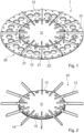
- the holding device designed as a turntable 1 in Fig. 1 comprises a flange 10 with a carrier plate 11, which in the embodiment is designed as a circular central plate. Twelve beams 13 extending outwards in a radial manner and projecting beyond the edge 12 of the carrier plate 11 are attached to the carrier plate 11.
- the beams 13 are designed, for example, as T-profile beams, the crossbeams 14 of which form the lower end.
- Each segment 20 has two circular openings 23 in its carrier 40, which are designed in a suitable manner to accommodate circular substrates (not shown).
- the segments 20 rest in their two lateral edge regions 21 on the crossbar 14 of a respective support 13.
- the supports 13 protrude, for example, beyond the edge 12 of the carrier plate 11 with such a length that they are flush with the segments 20.
- the components of the segments 20 as well as supports in the lateral edge region 21 are in Fig. 4 presented in detail and described there.
- Fig. 2 shows the carrier plate 11 with the supports 13 and the holding means 15 without segments 20.
- the Fig. 1 and Fig. 2 It can be seen that the carrier plate 11 has a suitable holding means 15 adjacent to the inner edge region 22 of each segment 20, which in the "closed" state, the segment 20 is held in the radial position shown and can at least be opened remotely and optionally also closed remotely.
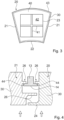
- Fig. 3 shows an alternative embodiment of a segment 20, which has the same dimensions, the same external shape and the same supports in the lateral edge area 21 as that of Fig. 1 and consequently alternatively to the latter in the holding device of the Fig. 1 can be used.
- the segment 20 comprises a segment support structure 30, which in the embodiment is designed in the form of a segment frame and on which a plate-shaped element 43 is mounted so that it covers the segment support structure 30 on at least one side.
- the plate-shaped element 43 forms the carrier 40.
- the carrier 40 has a rectangular opening 23 in the middle, which is divided into four carrier openings 42 by webs 41. Each carrier opening 42 is designed to accommodate a rectangular substrate (not shown).
- the segment 20 of Fig. 3 differs from those from Fig. 1 only by the shape of the opening 23, so that reference is made to the explanations therein. Instead of the square or round substrate shapes shown in the figures, any other geometries with the segments (20) can be arranged in the holding device.
- the cladding of the carrier 13 with respect to a coating can also be realized in another way and using other or additional components of the segments, for example by overlapping projections 26 of at least one lower plate-shaped element 43 and/or at least one segment support structure 30.
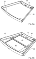
- Fig. 5A shows a segmental structure 30 as it is in Fig. 3 can be used.
- the segment support structure 30 has further holding means which serve to hold the carrier 40 on the segment support structure 30 and are to be referred to as carrier holding means 31.
- the carrier holding means 31 are designed as horizontal surfaces with screw connectors 33. Other carrier holding means are alternatively possible.
- Fig. 5B shows the segmental structure 30 of the Fig. 5A , supplemented by a carrier 40, which is mounted on the screw connectors 33 and covers the segment support structure 30 from below.
- the carrier 40 has a narrow bevel 45 at the level of the half of the segmental support structure 30.
- the bevel 45 has the same shielding effect as the projection 26 in Fig. 4 .
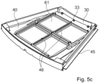
- the carrier 40 has two rectangular carrier openings 46 in the center, in each of which a pair of substrates 61 are arranged by means of holding frames 46 ( Fig. 5C ).
- the segments 20 thus equipped can be introduced into a treatment plant in order to be treated from below, for example coated.
- Fig. 6 shows an opened treatment plant 60, which has a holding device 1 according to Fig. 1
- the treatment plant 60 has a circular structure and has several stations 60' ... 60" distributed around its circumference, which serve directly or indirectly for the treatment of substrates 61.
- the substrates 61 are arranged in the segments 20 and are treated at at least one of the stations 60' ... 60"'. It is obvious that the treatment station 60 is closed during the treatment by means of its cover 63.
- the holding device 1 is equipped with the segments 20. Magazines (not shown) are arranged in a loading station 62, in which segments 20 with substrates 61 are stored.
- a suitable substrate transport device which carries out the rotation, the substrates 61 gradually pass through the individual stations 60' ... 60′′′′ including the Treatment station(s), so that the segments 20 with already treated substrates 61 can be removed from the loading station 62 and segments 20 with untreated substrates 61 can be mounted in the holding device 1.
Landscapes
- Engineering & Computer Science (AREA)
- Chemical & Material Sciences (AREA)
- Condensed Matter Physics & Semiconductors (AREA)
- General Physics & Mathematics (AREA)
- Manufacturing & Machinery (AREA)
- Computer Hardware Design (AREA)
- Microelectronics & Electronic Packaging (AREA)
- Power Engineering (AREA)
- Physics & Mathematics (AREA)
- Mechanical Engineering (AREA)
- Chemical Kinetics & Catalysis (AREA)
- Materials Engineering (AREA)
- Metallurgy (AREA)
- Organic Chemistry (AREA)
- Robotics (AREA)
- Container, Conveyance, Adherence, Positioning, Of Wafer (AREA)
- Physical Vapour Deposition (AREA)
Priority Applications (2)
| Application Number | Priority Date | Filing Date | Title |
|---|---|---|---|
| RS20250243A RS66601B1 (sr) | 2018-05-09 | 2019-05-09 | Uređaj za držanje za prihvatanje većeg broja podloga namenjen za njihovu obradu, sistem za obradu i postupak za obradu |
| HRP20250295TT HRP20250295T1 (hr) | 2018-05-09 | 2019-05-09 | Uređaj za držanje mnoštva podloga radi njihove obrade, postrojenje za obradu i postupak obrade |
Applications Claiming Priority (1)
| Application Number | Priority Date | Filing Date | Title |
|---|---|---|---|
| DE102018111247 | 2018-05-09 |
Publications (3)
| Publication Number | Publication Date |
|---|---|
| EP3567129A1 EP3567129A1 (de) | 2019-11-13 |
| EP3567129C0 EP3567129C0 (de) | 2024-12-11 |
| EP3567129B1 true EP3567129B1 (de) | 2024-12-11 |
Family
ID=66476456
Family Applications (1)
| Application Number | Title | Priority Date | Filing Date |
|---|---|---|---|
| EP19173443.3A Active EP3567129B1 (de) | 2018-05-09 | 2019-05-09 | Haltevorrichtung zur aufnahme mehrerer substrate zur behandlung derselben, behandlungsanlage und behandlungsverfahren |
Country Status (11)
| Country | Link |
|---|---|
| US (1) | US11332819B2 (pl) |
| EP (1) | EP3567129B1 (pl) |
| JP (1) | JP7442273B2 (pl) |
| KR (1) | KR102719516B1 (pl) |
| CN (1) | CN110473820B (pl) |
| DE (1) | DE102019112088A1 (pl) |
| HR (1) | HRP20250295T1 (pl) |
| HU (1) | HUE070507T2 (pl) |
| PL (1) | PL3567129T3 (pl) |
| RS (1) | RS66601B1 (pl) |
| TW (1) | TWI794475B (pl) |
Families Citing this family (6)
| Publication number | Priority date | Publication date | Assignee | Title |
|---|---|---|---|---|
| US20210220813A1 (en) * | 2020-01-16 | 2021-07-22 | Johnson Matthey Public Limited Company | Pallet for supporting a catalyst monolith during coating |
| TWI747611B (zh) * | 2020-11-13 | 2021-11-21 | 天虹科技股份有限公司 | 晶片預清潔機台 |
| TWI799120B (zh) * | 2020-11-13 | 2023-04-11 | 天虹科技股份有限公司 | 晶片預清潔機台 |
| TWI761270B (zh) * | 2020-11-13 | 2022-04-11 | 天虹科技股份有限公司 | 晶片預清潔機台 |
| WO2022128026A1 (de) * | 2020-12-17 | 2022-06-23 | Solayer Gmbh | Verfahren und vorrichtung zum wechsel von testsubstraten in einer vakuumdurchlaufanlage, behandlungsverfahren und vakuumdurchlaufanlage |
| DE102024113390A1 (de) * | 2024-05-14 | 2025-11-20 | VON ARDENNE Asset GmbH & Co. KG | Substratträger, Substratträger-Haltevorrichtung, Vakuumanordnung, Verwendung und Verfahren |
Family Cites Families (19)
| Publication number | Priority date | Publication date | Assignee | Title |
|---|---|---|---|---|
| US3396696A (en) * | 1966-10-06 | 1968-08-13 | Ralph F. Becker | Lens turner for high vacuum evaporators |
| NL7205670A (pl) * | 1972-03-16 | 1973-09-18 | ||
| CH668430A5 (de) * | 1986-07-31 | 1988-12-30 | Satis Vacuum Ag | Vakuum-beschichtungsanlage fuer optische substrate. |
| US4849250A (en) * | 1988-01-27 | 1989-07-18 | Storage Technology Corporation | Method and apparatus for producing magnetically oriented films on substrates |
| DE4110490C2 (de) * | 1991-03-30 | 2002-02-28 | Unaxis Deutschland Holding | Kathodenzerstäubungsanlage |
| US5911830A (en) * | 1996-05-09 | 1999-06-15 | Lucent Technologies Inc. | Method and fixture for laser bar facet coating |
| DE19822064A1 (de) * | 1998-05-16 | 1999-11-18 | Leybold Ag | Vorrichtung zum Halten von Linsen, insbesondere für in einer Vakuum-Aufdampfanlage oder Sputteranlage zu beschichtender Brillengläser |
| JP2002050678A (ja) * | 2000-08-02 | 2002-02-15 | Fujitsu Amd Semiconductor Kk | ウェーハ搬送体、ウェーハ搬送機構及び方法、及び半導体製造装置 |
| US6609877B1 (en) * | 2000-10-04 | 2003-08-26 | The Boc Group, Inc. | Vacuum chamber load lock structure and article transport mechanism |
| DE102006041137B4 (de) * | 2006-09-01 | 2015-02-12 | Carl Zeiss Vision Gmbh | Vorrichtung zum Wenden eines Gegenstands in einer Vakuumbeschichtungsanlage, Verfahren zum Wenden eines Gegenstands in einer Vakuumbeschichtungsanlage sowie deren Verwendung |
| JP5238657B2 (ja) * | 2009-09-17 | 2013-07-17 | 富士フイルム株式会社 | ワーク反転ユニット |
| JPWO2011013648A1 (ja) * | 2009-07-30 | 2013-01-07 | Hoya株式会社 | 光学レンズの蒸着装置 |
| TW201134967A (en) * | 2010-04-08 | 2011-10-16 | Hon Hai Prec Ind Co Ltd | Sputtering bracket and sputtering machine |
| CN103014617B (zh) * | 2011-09-22 | 2014-05-14 | 株式会社新柯隆 | 薄膜形成装置 |
| KR101928356B1 (ko) * | 2012-02-16 | 2018-12-12 | 엘지이노텍 주식회사 | 반도체 제조 장치 |
| US20140065303A1 (en) * | 2012-08-31 | 2014-03-06 | Robert Dennis Grejda | Holding device for optical element |
| EP3289113A1 (de) * | 2015-03-31 | 2018-03-07 | Bühler Alzenau GmbH | Verfahren zur herstellung von beschichteten substraten |
| TWM539150U (zh) * | 2016-11-21 | 2017-04-01 | 環球晶圓股份有限公司 | 晶圓承載盤 |
| US20190295880A1 (en) * | 2018-03-26 | 2019-09-26 | Veeco Instruments Inc. | Chemical vapor deposition wafer carrier with thermal cover |
-
2019
- 2019-04-17 TW TW108113470A patent/TWI794475B/zh active
- 2019-05-07 US US16/405,699 patent/US11332819B2/en active Active
- 2019-05-08 JP JP2019088367A patent/JP7442273B2/ja active Active
- 2019-05-08 KR KR1020190053775A patent/KR102719516B1/ko active Active
- 2019-05-09 HR HRP20250295TT patent/HRP20250295T1/hr unknown
- 2019-05-09 HU HUE19173443A patent/HUE070507T2/hu unknown
- 2019-05-09 EP EP19173443.3A patent/EP3567129B1/de active Active
- 2019-05-09 PL PL19173443.3T patent/PL3567129T3/pl unknown
- 2019-05-09 RS RS20250243A patent/RS66601B1/sr unknown
- 2019-05-09 DE DE102019112088.8A patent/DE102019112088A1/de active Pending
- 2019-05-09 CN CN201910384733.2A patent/CN110473820B/zh active Active
Also Published As
| Publication number | Publication date |
|---|---|
| EP3567129C0 (de) | 2024-12-11 |
| US20190345601A1 (en) | 2019-11-14 |
| PL3567129T3 (pl) | 2025-06-02 |
| CN110473820A (zh) | 2019-11-19 |
| DE102019112088A1 (de) | 2019-11-14 |
| KR20190129008A (ko) | 2019-11-19 |
| HRP20250295T1 (hr) | 2025-04-25 |
| US11332819B2 (en) | 2022-05-17 |
| KR102719516B1 (ko) | 2024-10-17 |
| RS66601B1 (sr) | 2025-04-30 |
| JP7442273B2 (ja) | 2024-03-04 |
| CN110473820B (zh) | 2024-09-27 |
| TW201947699A (zh) | 2019-12-16 |
| TWI794475B (zh) | 2023-03-01 |
| JP2019208019A (ja) | 2019-12-05 |
| EP3567129A1 (de) | 2019-11-13 |
| HUE070507T2 (hu) | 2025-06-28 |
Similar Documents
| Publication | Publication Date | Title |
|---|---|---|
| EP3567129B1 (de) | Haltevorrichtung zur aufnahme mehrerer substrate zur behandlung derselben, behandlungsanlage und behandlungsverfahren | |
| DE2454544C4 (de) | Vakuumbeschichtungsanlage | |
| CH673351A5 (pl) | ||
| DE4009603A1 (de) | Vorrichtung zum ein- und ausschleusen eines werkstuecks in eine vakuumkammer | |
| DE3047530A1 (de) | Vorrichtung zum unterstuetzen von mikroplaettchen | |
| DE112007002404T5 (de) | Verfahren zum Festhalten eines Siliciumwafers, Einspannvorrichtung zur Wärmebehandlung und wärmebehandelter Wafer | |
| CH691376A5 (de) | Vakuumanlage zur Oberflächenbearbeitung von Werkstücken. | |
| DE69810662T2 (de) | Anordnung zur ladung von gutträgern für thermische ofenbehandlungen | |
| EP3475472B1 (de) | Verfahren und vorrichtung zur herstellung von beschichteten halbleiterscheiben | |
| EP2815426B1 (de) | Prozessbox, anordnungen und verfahren zum prozessieren beschichteter substrate | |
| EP2764536A1 (de) | Substratwendeeinrichtung | |
| WO2005038077A2 (de) | Modulare vorrichtung zur beschichtung von oberflächen | |
| EP1435106B1 (de) | Hebe- und stützvorrichtung | |
| DE102010042839B4 (de) | Durchlauf-Vakuumbeschichtungsanlage zum Beschichten von Substraten | |
| EP1214733B1 (de) | Vorrichtung zum be- und entladen von substraten | |
| CH692741A5 (de) | Verfahren zur Herstellung in Vakuum oberflächenbehandelter Werkstücke und Vakuumbehandlungsanlage zu dessen Durchführung | |
| DE3242855A1 (de) | Verfahren und vorrichtung zur konturierung der dicke von aufgespruehten schichten | |
| DE3214256C2 (pl) | ||
| DE102010016325A1 (de) | Substratwendeeinrichtung | |
| EP1451817A1 (de) | Substrathalter | |
| DE102012110052B3 (de) | Batch-Anlage und Verfahren zur Behandlung von Substraten | |
| WO2019210907A1 (de) | Vakuumdurchlaufanlage mit hohem durchsatz | |
| DE102019214270A1 (de) | Laserbankvorrichtung und Fertigungsanlage | |
| EP4264662A1 (de) | Verfahren und vorrichtung zum wechsel von testsubstraten in einer vakuumdurchlaufanlage, behandlungsverfahren und vakuumdurchlaufanlage | |
| DE10135574B4 (de) | Verfahren und Vorrichtung zur Fertigung von Schichtstrukturen auf Substraten mittels Flüssigphasenepitaxie |
Legal Events
| Date | Code | Title | Description |
|---|---|---|---|
| PUAI | Public reference made under article 153(3) epc to a published international application that has entered the european phase |
Free format text: ORIGINAL CODE: 0009012 |
|
| STAA | Information on the status of an ep patent application or granted ep patent |
Free format text: STATUS: THE APPLICATION HAS BEEN PUBLISHED |
|
| AK | Designated contracting states |
Kind code of ref document: A1 Designated state(s): AL AT BE BG CH CY CZ DE DK EE ES FI FR GB GR HR HU IE IS IT LI LT LU LV MC MK MT NL NO PL PT RO RS SE SI SK SM TR |
|
| AX | Request for extension of the european patent |
Extension state: BA ME |
|
| STAA | Information on the status of an ep patent application or granted ep patent |
Free format text: STATUS: REQUEST FOR EXAMINATION WAS MADE |
|
| 17P | Request for examination filed |
Effective date: 20191210 |
|
| RBV | Designated contracting states (corrected) |
Designated state(s): AL AT BE BG CH CY CZ DE DK EE ES FI FR GB GR HR HU IE IS IT LI LT LU LV MC MK MT NL NO PL PT RO RS SE SI SK SM TR |
|
| STAA | Information on the status of an ep patent application or granted ep patent |
Free format text: STATUS: EXAMINATION IS IN PROGRESS |
|
| 17Q | First examination report despatched |
Effective date: 20220228 |
|
| GRAP | Despatch of communication of intention to grant a patent |
Free format text: ORIGINAL CODE: EPIDOSNIGR1 |
|
| STAA | Information on the status of an ep patent application or granted ep patent |
Free format text: STATUS: GRANT OF PATENT IS INTENDED |
|
| INTG | Intention to grant announced |
Effective date: 20240705 |
|
| RAP3 | Party data changed (applicant data changed or rights of an application transferred) |
Owner name: SOLAYER GMBH |
|
| GRAS | Grant fee paid |
Free format text: ORIGINAL CODE: EPIDOSNIGR3 |
|
| GRAA | (expected) grant |
Free format text: ORIGINAL CODE: 0009210 |
|
| STAA | Information on the status of an ep patent application or granted ep patent |
Free format text: STATUS: THE PATENT HAS BEEN GRANTED |
|
| AK | Designated contracting states |
Kind code of ref document: B1 Designated state(s): AL AT BE BG CH CY CZ DE DK EE ES FI FR GB GR HR HU IE IS IT LI LT LU LV MC MK MT NL NO PL PT RO RS SE SI SK SM TR |
|
| REG | Reference to a national code |
Ref country code: GB Ref legal event code: FG4D Free format text: NOT ENGLISH |
|
| REG | Reference to a national code |
Ref country code: CH Ref legal event code: EP |
|
| REG | Reference to a national code |
Ref country code: IE Ref legal event code: FG4D Free format text: LANGUAGE OF EP DOCUMENT: GERMAN |
|
| REG | Reference to a national code |
Ref country code: DE Ref legal event code: R096 Ref document number: 502019012627 Country of ref document: DE |
|
| U01 | Request for unitary effect filed |
Effective date: 20250110 |
|
| U07 | Unitary effect registered |
Designated state(s): AT BE BG DE DK EE FI FR IT LT LU LV MT NL PT RO SE SI Effective date: 20250117 |
|
| PG25 | Lapsed in a contracting state [announced via postgrant information from national office to epo] |
Ref country code: ES Free format text: LAPSE BECAUSE OF FAILURE TO SUBMIT A TRANSLATION OF THE DESCRIPTION OR TO PAY THE FEE WITHIN THE PRESCRIBED TIME-LIMIT Effective date: 20241211 |
|
| PG25 | Lapsed in a contracting state [announced via postgrant information from national office to epo] |
Ref country code: GR Free format text: LAPSE BECAUSE OF FAILURE TO SUBMIT A TRANSLATION OF THE DESCRIPTION OR TO PAY THE FEE WITHIN THE PRESCRIBED TIME-LIMIT Effective date: 20250312 |
|
| REG | Reference to a national code |
Ref country code: HR Ref legal event code: T1PR Ref document number: P20250295 Country of ref document: HR |
|
| REG | Reference to a national code |
Ref country code: SK Ref legal event code: T3 Ref document number: E 46085 Country of ref document: SK |
|
| REG | Reference to a national code |
Ref country code: HR Ref legal event code: ODRP Ref document number: P20250295 Country of ref document: HR Payment date: 20250429 Year of fee payment: 7 |
|
| REG | Reference to a national code |
Ref country code: HU Ref legal event code: AG4A Ref document number: E070507 Country of ref document: HU |
|
| PG25 | Lapsed in a contracting state [announced via postgrant information from national office to epo] |
Ref country code: SM Free format text: LAPSE BECAUSE OF FAILURE TO SUBMIT A TRANSLATION OF THE DESCRIPTION OR TO PAY THE FEE WITHIN THE PRESCRIBED TIME-LIMIT Effective date: 20241211 |
|
| PGFP | Annual fee paid to national office [announced via postgrant information from national office to epo] |
Ref country code: PL Payment date: 20250425 Year of fee payment: 7 |
|
| U20 | Renewal fee for the european patent with unitary effect paid |
Year of fee payment: 7 Effective date: 20250530 |
|
| PGFP | Annual fee paid to national office [announced via postgrant information from national office to epo] |
Ref country code: GB Payment date: 20250522 Year of fee payment: 7 |
|
| PG25 | Lapsed in a contracting state [announced via postgrant information from national office to epo] |
Ref country code: IS Free format text: LAPSE BECAUSE OF FAILURE TO SUBMIT A TRANSLATION OF THE DESCRIPTION OR TO PAY THE FEE WITHIN THE PRESCRIBED TIME-LIMIT Effective date: 20250411 |
|
| PGFP | Annual fee paid to national office [announced via postgrant information from national office to epo] |
Ref country code: RS Payment date: 20250425 Year of fee payment: 7 Ref country code: NO Payment date: 20250520 Year of fee payment: 7 |
|
| PGFP | Annual fee paid to national office [announced via postgrant information from national office to epo] |
Ref country code: HR Payment date: 20250429 Year of fee payment: 7 |
|
| PGFP | Annual fee paid to national office [announced via postgrant information from national office to epo] |
Ref country code: HU Payment date: 20250505 Year of fee payment: 7 |
|
| PGFP | Annual fee paid to national office [announced via postgrant information from national office to epo] |
Ref country code: CH Payment date: 20250601 Year of fee payment: 7 |
|
| PGFP | Annual fee paid to national office [announced via postgrant information from national office to epo] |
Ref country code: TR Payment date: 20250505 Year of fee payment: 7 Ref country code: SK Payment date: 20250430 Year of fee payment: 7 |
|
| PGFP | Annual fee paid to national office [announced via postgrant information from national office to epo] |
Ref country code: CZ Payment date: 20250428 Year of fee payment: 7 |
|
| PGFP | Annual fee paid to national office [announced via postgrant information from national office to epo] |
Ref country code: IE Payment date: 20250522 Year of fee payment: 7 |
|
| PLBE | No opposition filed within time limit |
Free format text: ORIGINAL CODE: 0009261 |
|
| STAA | Information on the status of an ep patent application or granted ep patent |
Free format text: STATUS: NO OPPOSITION FILED WITHIN TIME LIMIT |
|
| 26N | No opposition filed |
Effective date: 20250912 |