EP3553825A1 - Dünnschicht-verpackungsstruktur, dünnschicht-verpackungsverfahren und anzeigetafel - Google Patents
Dünnschicht-verpackungsstruktur, dünnschicht-verpackungsverfahren und anzeigetafel Download PDFInfo
- Publication number
- EP3553825A1 EP3553825A1 EP18850337.9A EP18850337A EP3553825A1 EP 3553825 A1 EP3553825 A1 EP 3553825A1 EP 18850337 A EP18850337 A EP 18850337A EP 3553825 A1 EP3553825 A1 EP 3553825A1
- Authority
- EP
- European Patent Office
- Prior art keywords
- thin film
- groove structure
- display region
- adhesive layer
- organic adhesive
- Prior art date
- Legal status (The legal status is an assumption and is not a legal conclusion. Google has not performed a legal analysis and makes no representation as to the accuracy of the status listed.)
- Ceased
Links
Images


Classifications
-
- H—ELECTRICITY
- H10—SEMICONDUCTOR DEVICES; ELECTRIC SOLID-STATE DEVICES NOT OTHERWISE PROVIDED FOR
- H10K—ORGANIC ELECTRIC SOLID-STATE DEVICES
- H10K59/00—Integrated devices, or assemblies of multiple devices, comprising at least one organic light-emitting element covered by group H10K50/00
- H10K59/80—Constructional details
- H10K59/87—Passivation; Containers; Encapsulations
- H10K59/873—Encapsulations
- H10K59/8731—Encapsulations multilayered coatings having a repetitive structure, e.g. having multiple organic-inorganic bilayers
-
- H—ELECTRICITY
- H10—SEMICONDUCTOR DEVICES; ELECTRIC SOLID-STATE DEVICES NOT OTHERWISE PROVIDED FOR
- H10K—ORGANIC ELECTRIC SOLID-STATE DEVICES
- H10K50/00—Organic light-emitting devices
- H10K50/80—Constructional details
- H10K50/84—Passivation; Containers; Encapsulations
- H10K50/842—Containers
- H10K50/8426—Peripheral sealing arrangements, e.g. adhesives, sealants
-
- H—ELECTRICITY
- H10—SEMICONDUCTOR DEVICES; ELECTRIC SOLID-STATE DEVICES NOT OTHERWISE PROVIDED FOR
- H10K—ORGANIC ELECTRIC SOLID-STATE DEVICES
- H10K50/00—Organic light-emitting devices
- H10K50/80—Constructional details
- H10K50/84—Passivation; Containers; Encapsulations
- H10K50/844—Encapsulations
- H10K50/8445—Encapsulations multilayered coatings having a repetitive structure, e.g. having multiple organic-inorganic bilayers
-
- H—ELECTRICITY
- H10—SEMICONDUCTOR DEVICES; ELECTRIC SOLID-STATE DEVICES NOT OTHERWISE PROVIDED FOR
- H10K—ORGANIC ELECTRIC SOLID-STATE DEVICES
- H10K59/00—Integrated devices, or assemblies of multiple devices, comprising at least one organic light-emitting element covered by group H10K50/00
- H10K59/10—OLED displays
- H10K59/12—Active-matrix OLED [AMOLED] displays
- H10K59/122—Pixel-defining structures or layers, e.g. banks
-
- H—ELECTRICITY
- H10—SEMICONDUCTOR DEVICES; ELECTRIC SOLID-STATE DEVICES NOT OTHERWISE PROVIDED FOR
- H10K—ORGANIC ELECTRIC SOLID-STATE DEVICES
- H10K71/00—Manufacture or treatment specially adapted for the organic devices covered by this subclass
-
- H—ELECTRICITY
- H10—SEMICONDUCTOR DEVICES; ELECTRIC SOLID-STATE DEVICES NOT OTHERWISE PROVIDED FOR
- H10K—ORGANIC ELECTRIC SOLID-STATE DEVICES
- H10K59/00—Integrated devices, or assemblies of multiple devices, comprising at least one organic light-emitting element covered by group H10K50/00
- H10K59/80—Constructional details
- H10K59/87—Passivation; Containers; Encapsulations
- H10K59/871—Self-supporting sealing arrangements
- H10K59/8722—Peripheral sealing arrangements, e.g. adhesives, sealants
Definitions
- the present application relates to the field of display technologies, and in particular, to a thin film package structure, a thin film package method, and a display panel.
- An organic light-emitting device is a current-type semiconductor light-emitting device. Due to advantages such as active illumination, high luminous efficiency, and no limitation on the viewing angle, the organic light-emitting device is widely applied in lighting and display fields.
- the organic light-emitting device emits light by using an organic light-emitting diode (OLED) therein.
- OLED organic light-emitting diode
- the OLED is sensitive to external factors such as water vapor and oxygen, and may be reduced in stability and lifespan if exposed to the water vapor and oxygen. Therefore, the use of an effective package structure can prevent entering of water vapor and oxygen, and prolong the lifespan of the OLED.
- a method that has a desirable effect is alternately stacking an organic layer and an inorganic layer.
- This method can enhance the flexibility of the inorganic layer to prevent the inorganic layer from easily breaking, and further strengthen the resistance of the organic layer to water vapor and oxygen.
- the water vapor and oxygen from the periphery area of the OLED can easily enter into the OLED through gaps between the organic layers and the inorganic layers, leading to a reduction of the luminous performance of the OLED. More seriously, the whole organic light-emitting device is likely to shut down.
- An objective of the present application is to provide a package structure, which prolongs a path through which water vapor and oxygen enter into a flexible display device, lowers an influence of the water vapor and oxygen on the flexible display device, and further improves an anti-bending ability of the display device.
- Another objective of the present application is to provide a display panel, which prolongs a path through which water vapor and oxygen enter into a flexible display device, lowers an influence of the water vapor and oxygen on the flexible display device, and further improves an anti-bending ability of the display device.
- a thin film package structure includes: a substrate, an organic adhesive layer, and a package film layer, wherein the organic adhesive layer is provided on the substrate, the package film layer covers the organic adhesive layer, and the organic adhesive layer is formed with a groove structure.
- the groove structure is an uncrossed groove structure that extends in a zigzag form.
- the groove structure is a crossed groove structure with a grid shape.
- the substrate includes a display region and a non-display region surrounding the display region; and the organic adhesive layer is formed with an embankment structure which surrounds the display region.
- the embankment structure and the groove structure are arranged side by side.
- the groove structure is disposed in the embankment structure.
- the groove structure is a continuous groove structure.
- the groove structure is a discontinuous groove structure disposed in the embankment structure in a separated manner.
- the present application also provides a display panel, which is packaged by comprising the thin film package structure described above.
- the present application also provides a thin film package method, used to realize a packaging to form a display panel, wherein the display panel includes a display region and a non-display region surrounding the display region, and the thin film package method includes the following steps:
- an inorganic layer in the package film layer can be in contact with the substrate to realize a sealing. Since the substrate and the package film layer have a first layer deposited by the inorganic layer, a package effect can be effectively improved, and water and oxygen are prevented from entering.
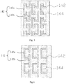
- FIG. 1 is a schematic top view of a display panel of the present application.
- FIG. 2 is a cross-sectional schematic view along the line II-II in FIG. 1 .
- the present application provides a display panel 10, which includes a substrate 12.
- the substrate 12 includes a display region 101 and a non-display region 102 surrounding the display region 101.
- a light-emitting device 18 is provided on the display region 101 of the substrate 12, and the substrate 12 is covered with a package film layer 16.
- the package film layer 16 covers the non-display region 102 and the light-emitting device 18.
- the package film layer 16 is formed by alternately stacking an inorganic layer and an organic layer.
- an organic adhesive layer 14 is provided between the package film layer 16 and the substrate 12.
- the organic adhesive layer 14 is arranged in the non-display region 102 of the substrate 12.
- the organic adhesive layer 14 is provided on the substrate 12, and is arranged in the non-display region 102.
- the organic adhesive layer 14 is formed with a groove structure 142 and/or an embankment structure 144.
- the groove structure 142 exposes the substrate 12, and the groove structure 142 is filled by the package film layer 16 in the non-display region 102.
- the groove structure 142 is an uncrossed groove structure that extends in a zigzag form. In other embodiments of the present application, the groove structure 142 may also be a crossed groove structure that extends in a zigzag form.
- the organic adhesive layer 14 is designed to also have an embankment structure 144 which surrounds the display region 101. The embankment structure 144 and the groove structure 142 are arranged side by side. The groove structure 142 is disposed in the embankment structure 144, and is a continuous groove structure.
- the groove structure 142 may also be a discontinuous groove structure disposed in the embankment structure 144 in a separated manner.
- the groove structure 142 may also be a crossed groove structure with a grid shape.
- a thin film package structure includes a substrate 12, an organic adhesive layer 14, and a package film layer 16.
- the organic adhesive layer 14 is provided on the substrate 12, and the package film layer 16 covers the substrate 12 and the organic adhesive layer 14.
- the organic adhesive layer 14 is disposed in the non-display region 102, and is designed to have the groove structure 142 and the embankment structure 144 defined by the groove structure 142.
- the groove structure 142 and the embankment structure 144 surround the display region 101.
- At least one of the groove structure 142 and the embankment structure 144 is a structure extending in a zigzag form or a grid-shaped structure.
- the groove structure 142 and the embankment structure 144 surround the display region 101 in a square shape.
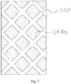
- FIG. 3 is a schematic top view of an organic adhesive layer in the region III in FIG. 1 .
- the groove structure 142 and the embankment structure 144 are both in a structure extending in a zigzag form.
- the at least two groove structures 142 and the at least two embankment structures 144 are alternately arranged from the edge of the display panel 10 towards the center of the display panel 10.
- the groove structure 142 includes multiple first grooves 142a and multiple second grooves 142b.
- the multiple first grooves 142a and the multiple second grooves 142b are concavely designed in reverse directions and are alternately arranged along an extension direction of the groove structure 142.
- the multiple first grooves 142a and the multiple second grooves 142b are in regular shapes or irregular shapes.
- the groove structure 142 may also be a structure that is formed by alternately arranging multiple first grooves 142a and multiple second grooves 142b and extends in a zigzag form, as shown in FIGs. 4 , 5, and 6 .
- the first grooves 142a and the second grooves 142b may be formed by bending a linear groove.
- the first grooves 142a and the second grooves 142b may be integrally formed. That is, the first grooves 142a and the second grooves 142b may integrally serve as a repetitive unit.
- the groove structure 142 may be a grid-shaped structure.
- the embankment structure 144 includes multiple block structures 144a which are disconnected and each of the multiple block structures 144a is separately embedded in the mesh of the groove structure 142, as shown in FIG. 7 .
- the embankment structure 144 is a grid-shaped structure.
- the groove structure 142 includes multiple grooves 142c which are disconnected and each of the multiple grooves 142c is separately embedded in the mesh of the embankment structure 144, as shown in FIG. 8 .
- the grooves 142c in one column may also be interconnected so as to form a combined structure with the grooves 142c in the adjacent column that are disconnected, as shown in FIG. 9 .
- the organic adhesive layer 14 in the non-display region 102 of the substrate 12 is designed to have groove structures 142, such that a water-oxygen diffusion path is more tortuous.
- a water-oxygen permeation path is prolonged and a package effect of the display panel 10 is improved.
- the bending stress produced in bending of an edge region of the display panel 10 can be reduced or decentralized so that the bending performance of the edge region of the display panel 10 can be improved.
- the groove structures and the embankment structures 144 are arranged around the display region 101 by a nested combination, so that a small space is taken up, a width limitation on the non-display region 102 caused by arranging multiple barriers around a screen to prevent entering of water and oxygen in the prior art is eliminated and a narrow bezel design is realized.
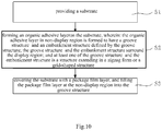
- the present application also provides a thin film package method, used to realize a packaging to form a display panel 10.
- the display panel 10 includes a display region 101 and a non-display region 102 surrounding the display region 101.
- the thin film package method includes the following steps:
- the present application also provides a display panel 10, which includes a light-emitting display device 18 and the above-described thin film package structure for packaging the light-emitting display device 18.
- the organic adhesive layer 14 in the non-display region 102 of the substrate 12 is designed to have groove structures 142, such that a water-oxygen diffusion path is more tortuous.
- a water-oxygen permeation path is prolonged and a package effect of the display panel 10 is improved.
- the bending stress produced in bending of an edge region of the display panel 10 can be reduced or decentralized, thus the bending performance of the edge region of the display panel 10 is improved.
- the groove structures and the embankment structures 144 are arranged around the display region 101 by a nested combination, so that a small space is integrally taken up, a width limitation on the non-display region 102 caused by arranging multiple barriers around a screen to prevent entering of water and oxygen in the prior art is eliminated, and a narrow bezel design is realized.
Landscapes
- Chemical & Material Sciences (AREA)
- Inorganic Chemistry (AREA)
- Physics & Mathematics (AREA)
- Optics & Photonics (AREA)
- Engineering & Computer Science (AREA)
- Microelectronics & Electronic Packaging (AREA)
- Manufacturing & Machinery (AREA)
- Electroluminescent Light Sources (AREA)
- Devices For Indicating Variable Information By Combining Individual Elements (AREA)
Applications Claiming Priority (2)
| Application Number | Priority Date | Filing Date | Title |
|---|---|---|---|
| CN201710772356.0A CN107689425A (zh) | 2017-08-31 | 2017-08-31 | 薄膜封装结构及薄膜封装方法和显示面板 |
| PCT/CN2018/085052 WO2019041864A1 (zh) | 2017-08-31 | 2018-04-28 | 薄膜封装结构及薄膜封装方法和显示面板 |
Publications (2)
| Publication Number | Publication Date |
|---|---|
| EP3553825A1 true EP3553825A1 (de) | 2019-10-16 |
| EP3553825A4 EP3553825A4 (de) | 2020-02-19 |
Family
ID=61155934
Family Applications (1)
| Application Number | Title | Priority Date | Filing Date |
|---|---|---|---|
| EP18850337.9A Ceased EP3553825A4 (de) | 2017-08-31 | 2018-04-28 | Dünnschicht-verpackungsstruktur, dünnschicht-verpackungsverfahren und anzeigetafel |
Country Status (7)
| Country | Link |
|---|---|
| US (1) | US11374201B2 (de) |
| EP (1) | EP3553825A4 (de) |
| JP (1) | JP6865834B2 (de) |
| KR (1) | KR102245486B1 (de) |
| CN (1) | CN107689425A (de) |
| TW (1) | TWI725307B (de) |
| WO (1) | WO2019041864A1 (de) |
Cited By (1)
| Publication number | Priority date | Publication date | Assignee | Title |
|---|---|---|---|---|
| US11917851B2 (en) | 2019-03-29 | 2024-02-27 | Hefei Xinsheng Optoelectronics Technology Co., Ltd. | Packaging structure, display substrate, display apparatus and method for packaging display device |
Families Citing this family (35)
| Publication number | Priority date | Publication date | Assignee | Title |
|---|---|---|---|---|
| JP5016832B2 (ja) * | 2006-03-27 | 2012-09-05 | 株式会社東芝 | 不揮発性半導体記憶装置及びその製造方法 |
| CN107689425A (zh) | 2017-08-31 | 2018-02-13 | 昆山国显光电有限公司 | 薄膜封装结构及薄膜封装方法和显示面板 |
| CN108461645A (zh) * | 2018-02-09 | 2018-08-28 | 武汉华星光电半导体显示技术有限公司 | 一种用于柔性显示器件上的封装结构及制备方法 |
| WO2019214285A1 (zh) * | 2018-05-11 | 2019-11-14 | 云谷(固安)科技有限公司 | 显示面板母板、显示面板及显示面板制备方法 |
| US10783825B2 (en) | 2018-05-14 | 2020-09-22 | Kunshan Go-Visionox Opto-Electronics Co., Ltd. | Driving substrates and display panels |
| CN108666442B (zh) * | 2018-05-14 | 2020-04-21 | 昆山国显光电有限公司 | 驱动基板和显示面板 |
| CN108777266B (zh) * | 2018-05-30 | 2020-04-24 | 上海天马微电子有限公司 | 一种显示面板及显示装置 |
| CN108832028B (zh) * | 2018-06-11 | 2020-08-04 | 武汉华星光电半导体显示技术有限公司 | 一种oled显示面板的制备方法及oled显示面板、显示装置 |
| CN108832018A (zh) * | 2018-06-21 | 2018-11-16 | 北京蜃景光电科技有限公司 | 一种具有增强密封效果的有机发光器件、显示屏和显示器 |
| CN108847136A (zh) * | 2018-06-29 | 2018-11-20 | 京东方科技集团股份有限公司 | 电子设备 |
| CN109256481B (zh) * | 2018-08-30 | 2020-09-11 | 云谷(固安)科技有限公司 | 显示面板和显示装置 |
| CN109461833B (zh) * | 2018-08-31 | 2020-09-04 | 云谷(固安)科技有限公司 | 显示面板及其制造方法 |
| WO2020073315A1 (zh) * | 2018-10-12 | 2020-04-16 | 深圳柔显系统技术有限公司 | 触控面板及触控装置 |
| CN109378405B (zh) * | 2018-10-18 | 2023-01-13 | 京东方科技集团股份有限公司 | 一种柔性显示面板及显示装置 |
| CN111082768B (zh) * | 2018-10-19 | 2023-10-27 | 天津大学 | 封装结构及具有其的半导体器件、具有半导体器件的电子设备 |
| CN109686855A (zh) * | 2018-12-04 | 2019-04-26 | 武汉华星光电半导体显示技术有限公司 | 一种薄膜封装结构及薄膜封装方法 |
| CN109523922B (zh) * | 2018-12-14 | 2021-08-17 | 云谷(固安)科技有限公司 | 一种柔性模组、显示面板和显示装置 |
| CN109557725A (zh) * | 2018-12-19 | 2019-04-02 | 惠科股份有限公司 | 显示面板、显示装置以及显示面板的制造方法 |
| CN109686862A (zh) * | 2019-01-10 | 2019-04-26 | 武汉华星光电半导体显示技术有限公司 | 显示面板 |
| CN109888125B (zh) * | 2019-02-28 | 2021-06-22 | 武汉华星光电半导体显示技术有限公司 | 一种显示面板及其制作方法 |
| CN110323196B (zh) * | 2019-05-09 | 2021-11-16 | 京东方科技集团股份有限公司 | 一种显示基板及其制备方法、显示装置 |
| CN110190102A (zh) * | 2019-05-29 | 2019-08-30 | 武汉华星光电半导体显示技术有限公司 | 一种可折叠的显示面板及其制作方法 |
| CN110444681B (zh) * | 2019-07-22 | 2020-12-08 | 武汉华星光电半导体显示技术有限公司 | 发光面板及显示设备 |
| CN110611042B (zh) * | 2019-08-26 | 2020-10-27 | 武汉华星光电半导体显示技术有限公司 | 一种柔性衬底基板、柔性显示面板及其制备方法 |
| CN113517410A (zh) * | 2020-04-10 | 2021-10-19 | 华为技术有限公司 | 柔性显示面板、显示模组和移动终端 |
| CN112396963A (zh) * | 2020-11-16 | 2021-02-23 | 武汉华星光电半导体显示技术有限公司 | 可折叠显示模组及装置 |
| CN112435581B (zh) * | 2020-11-30 | 2023-01-13 | 京东方科技集团股份有限公司 | 一种柔性显示结构、柔性显示屏及电子设备 |
| CN112954929A (zh) * | 2021-01-29 | 2021-06-11 | 厦门天马微电子有限公司 | 显示模组及显示装置 |
| CN113193137B (zh) * | 2021-04-07 | 2022-05-31 | 深圳市华星光电半导体显示技术有限公司 | 显示面板及显示面板的封装结构制备方法 |
| CN113257132A (zh) * | 2021-05-24 | 2021-08-13 | 昆山国显光电有限公司 | 滑移显示装置 |
| US12490633B2 (en) | 2021-11-25 | 2025-12-02 | Chengdu Boe Optoelectronics Technology Co., Ltd. | Display panel and display device |
| CN115279013A (zh) * | 2022-05-31 | 2022-11-01 | 青岛歌尔微电子研究院有限公司 | 选择性封装结构及封装结构的制备方法 |
| CN116347957A (zh) * | 2023-02-15 | 2023-06-27 | 安徽芯视佳半导体显示科技有限公司 | 一种硅基oled封装结构及封装方法 |
| CN120076646A (zh) * | 2023-11-30 | 2025-05-30 | 京东方科技集团股份有限公司 | 显示面板及显示装置 |
| TWI894902B (zh) * | 2024-04-03 | 2025-08-21 | 元太科技工業股份有限公司 | 可撓式顯示裝置 |
Family Cites Families (23)
| Publication number | Priority date | Publication date | Assignee | Title |
|---|---|---|---|---|
| KR100751376B1 (ko) | 2006-04-05 | 2007-08-22 | 삼성에스디아이 주식회사 | 장수명의 평판표시장치 |
| KR100943185B1 (ko) * | 2008-04-24 | 2010-02-19 | 삼성모바일디스플레이주식회사 | 유기 발광 디스플레이 장치 |
| TWI436312B (zh) * | 2009-03-04 | 2014-05-01 | Prime View Int Co Ltd | 可撓式顯示器 |
| TWI389271B (zh) * | 2009-04-10 | 2013-03-11 | 財團法人工業技術研究院 | 環境敏感電子元件之封裝體及其封裝方法 |
| TWI466243B (zh) * | 2010-09-10 | 2014-12-21 | Ind Tech Res Inst | 環境敏感電子元件之封裝體及其封裝方法 |
| TWI473264B (zh) * | 2012-03-02 | 2015-02-11 | Au Optronics Corp | 有機電致發光裝置 |
| CN103794733A (zh) | 2012-10-31 | 2014-05-14 | 财团法人工业技术研究院 | 环境敏感电子元件封装体 |
| KR102111562B1 (ko) * | 2013-04-25 | 2020-05-18 | 삼성디스플레이 주식회사 | 표시 장치 |
| TWI515937B (zh) | 2013-05-15 | 2016-01-01 | 緯創資通股份有限公司 | 有機光電元件之封裝結構以及封裝方法 |
| KR102117612B1 (ko) * | 2013-08-28 | 2020-06-02 | 삼성디스플레이 주식회사 | 유기 발광 표시 장치 및 이의 제조 방법 |
| JP2016091630A (ja) | 2014-10-30 | 2016-05-23 | 凸版印刷株式会社 | フレキシブル有機elシートおよびその封止方法 |
| KR102345004B1 (ko) * | 2015-02-26 | 2021-12-29 | 삼성디스플레이 주식회사 | 유기 발광 표시 장치 |
| CN105140418A (zh) | 2015-08-25 | 2015-12-09 | 深圳市华星光电技术有限公司 | 有机发光二极管封装件及包括其的显示装置 |
| CN106847855B (zh) * | 2015-12-07 | 2019-09-17 | 昆山工研院新型平板显示技术中心有限公司 | Oled显示面板及其封装方法 |
| JP2017147165A (ja) * | 2016-02-19 | 2017-08-24 | 株式会社ジャパンディスプレイ | 表示装置 |
| CN205789979U (zh) * | 2016-05-30 | 2016-12-07 | 鄂尔多斯市源盛光电有限责任公司 | 一种有机发光显示器件面板、显示设备 |
| CN205985076U (zh) * | 2016-08-30 | 2017-02-22 | 昆山国显光电有限公司 | 有机发光显示装置及薄膜封装结构 |
| CN106816551B (zh) * | 2016-12-29 | 2018-09-21 | 上海天马有机发光显示技术有限公司 | Oled显示基板及显示装置 |
| CN106997930B (zh) * | 2017-03-03 | 2019-04-12 | 上海天马有机发光显示技术有限公司 | 柔性显示面板及显示装置 |
| CN106981584B (zh) * | 2017-03-20 | 2019-11-26 | 上海天马有机发光显示技术有限公司 | 柔性有机发光二极管显示面板、显示装置及其制作方法 |
| CN106848107A (zh) * | 2017-04-27 | 2017-06-13 | 上海天马微电子有限公司 | 一种有机发光显示面板及有机发光显示装置 |
| CN207381403U (zh) * | 2017-08-31 | 2018-05-18 | 京东方科技集团股份有限公司 | 显示基板、显示面板 |
| CN107689425A (zh) * | 2017-08-31 | 2018-02-13 | 昆山国显光电有限公司 | 薄膜封装结构及薄膜封装方法和显示面板 |
-
2017
- 2017-08-31 CN CN201710772356.0A patent/CN107689425A/zh active Pending
-
2018
- 2018-04-28 EP EP18850337.9A patent/EP3553825A4/de not_active Ceased
- 2018-04-28 US US16/324,652 patent/US11374201B2/en active Active
- 2018-04-28 WO PCT/CN2018/085052 patent/WO2019041864A1/zh not_active Ceased
- 2018-04-28 JP JP2019537151A patent/JP6865834B2/ja active Active
- 2018-04-28 KR KR1020197019719A patent/KR102245486B1/ko active Active
- 2018-05-09 TW TW107115757A patent/TWI725307B/zh active
Cited By (1)
| Publication number | Priority date | Publication date | Assignee | Title |
|---|---|---|---|---|
| US11917851B2 (en) | 2019-03-29 | 2024-02-27 | Hefei Xinsheng Optoelectronics Technology Co., Ltd. | Packaging structure, display substrate, display apparatus and method for packaging display device |
Also Published As
| Publication number | Publication date |
|---|---|
| WO2019041864A1 (zh) | 2019-03-07 |
| KR20190089067A (ko) | 2019-07-29 |
| KR102245486B1 (ko) | 2021-04-29 |
| US11374201B2 (en) | 2022-06-28 |
| CN107689425A (zh) | 2018-02-13 |
| JP2020505720A (ja) | 2020-02-20 |
| US20210336216A1 (en) | 2021-10-28 |
| JP6865834B2 (ja) | 2021-04-28 |
| EP3553825A4 (de) | 2020-02-19 |
| TW201842666A (zh) | 2018-12-01 |
| TWI725307B (zh) | 2021-04-21 |
Similar Documents
| Publication | Publication Date | Title |
|---|---|---|
| US11374201B2 (en) | Thin film package structure, thin film package method, and display panel | |
| TWI634468B (zh) | 透明顯示裝置 | |
| EP3154088B1 (de) | Lichtemittierende anzeigetafel und herstellungsverfahren dafür | |
| TWI492436B (zh) | 可撓式顯示面板 | |
| CN209328948U (zh) | 一种显示面板 | |
| CN111416063B (zh) | 柔性oled显示面板及其制备方法 | |
| CN206282861U (zh) | 一种有机发光显示面板及装置 | |
| KR20220124667A (ko) | 표시 장치 | |
| TWI637657B (zh) | 有機發光二極體顯示器 | |
| US20160284770A1 (en) | Flexible display device | |
| KR20200013819A (ko) | 전계 발광 장치 | |
| KR20190048776A (ko) | 투명 디스플레이 장치 | |
| CN106450038A (zh) | 显示面板及其制造方法、显示装置 | |
| CN206282888U (zh) | 一种柔性显示面板和显示装置 | |
| CN110211998A (zh) | 一种有机发光显示面板及显示装置 | |
| CN106816456A (zh) | 一种有机发光二极管显示面板及显示器 | |
| KR20140124614A (ko) | 유기 발광 표시 장치 | |
| KR20180062548A (ko) | 유기발광 표시장치 | |
| CN110943108A (zh) | 一种折叠显示面板及其制作方法、显示装置 | |
| CN107799665A (zh) | 薄膜封装结构、显示器件及封装方法 | |
| CN110335958A (zh) | 有机发光显示面板及其制造方法、封装薄膜 | |
| CN101983399A (zh) | 发光二极管装置 | |
| US20160260927A1 (en) | Flexible display device | |
| CN117642027A (zh) | 显示面板和显示装置 | |
| KR20150070544A (ko) | 유기 발광 표시장치 및 그 제조방법 |
Legal Events
| Date | Code | Title | Description |
|---|---|---|---|
| STAA | Information on the status of an ep patent application or granted ep patent |
Free format text: STATUS: THE INTERNATIONAL PUBLICATION HAS BEEN MADE |
|
| PUAI | Public reference made under article 153(3) epc to a published international application that has entered the european phase |
Free format text: ORIGINAL CODE: 0009012 |
|
| STAA | Information on the status of an ep patent application or granted ep patent |
Free format text: STATUS: REQUEST FOR EXAMINATION WAS MADE |
|
| 17P | Request for examination filed |
Effective date: 20190711 |
|
| AK | Designated contracting states |
Kind code of ref document: A1 Designated state(s): AL AT BE BG CH CY CZ DE DK EE ES FI FR GB GR HR HU IE IS IT LI LT LU LV MC MK MT NL NO PL PT RO RS SE SI SK SM TR |
|
| AX | Request for extension of the european patent |
Extension state: BA ME |
|
| A4 | Supplementary search report drawn up and despatched |
Effective date: 20200121 |
|
| RIC1 | Information provided on ipc code assigned before grant |
Ipc: H01L 51/52 20060101ALI20200115BHEP Ipc: H01L 27/32 20060101AFI20200115BHEP |
|
| DAV | Request for validation of the european patent (deleted) | ||
| DAX | Request for extension of the european patent (deleted) | ||
| STAA | Information on the status of an ep patent application or granted ep patent |
Free format text: STATUS: EXAMINATION IS IN PROGRESS |
|
| 17Q | First examination report despatched |
Effective date: 20220208 |
|
| REG | Reference to a national code |
Ref country code: DE Ref legal event code: R003 |
|
| STAA | Information on the status of an ep patent application or granted ep patent |
Free format text: STATUS: THE APPLICATION HAS BEEN REFUSED |
|
| 18R | Application refused |
Effective date: 20240514 |