EP3540436A1 - Capteur moléculaire haute résolution - Google Patents
Capteur moléculaire haute résolution Download PDFInfo
- Publication number
- EP3540436A1 EP3540436A1 EP19172912.8A EP19172912A EP3540436A1 EP 3540436 A1 EP3540436 A1 EP 3540436A1 EP 19172912 A EP19172912 A EP 19172912A EP 3540436 A1 EP3540436 A1 EP 3540436A1
- Authority
- EP
- European Patent Office
- Prior art keywords
- graphene
- thickness
- nanopore
- molecular
- translocation
- Prior art date
- Legal status (The legal status is an assumption and is not a legal conclusion. Google has not performed a legal analysis and makes no representation as to the accuracy of the status listed.)
- Granted
Links
- 230000005945 translocation Effects 0.000 claims abstract description 75
- 230000008859 change Effects 0.000 claims abstract description 55
- 239000007787 solid Substances 0.000 claims abstract description 6
- 238000000034 method Methods 0.000 claims description 57
- 108020004414 DNA Proteins 0.000 claims description 34
- 239000002773 nucleotide Substances 0.000 claims description 24
- 125000003729 nucleotide group Chemical group 0.000 claims description 24
- 102000053602 DNA Human genes 0.000 claims description 12
- 108091034117 Oligonucleotide Proteins 0.000 claims description 10
- 238000007479 molecular analysis Methods 0.000 claims description 6
- OKTJSMMVPCPJKN-UHFFFAOYSA-N Carbon Chemical compound [C] OKTJSMMVPCPJKN-UHFFFAOYSA-N 0.000 abstract description 158
- 229910021389 graphene Inorganic materials 0.000 abstract description 145
- 230000005669 field effect Effects 0.000 abstract description 9
- 239000010410 layer Substances 0.000 description 88
- 241000894007 species Species 0.000 description 64
- 239000000463 material Substances 0.000 description 49
- 239000012528 membrane Substances 0.000 description 45
- 239000000758 substrate Substances 0.000 description 23
- 150000004767 nitrides Chemical class 0.000 description 20
- 230000008569 process Effects 0.000 description 15
- 230000015572 biosynthetic process Effects 0.000 description 13
- 229910002804 graphite Inorganic materials 0.000 description 13
- 239000010439 graphite Substances 0.000 description 13
- 229910004205 SiNX Inorganic materials 0.000 description 11
- XUIMIQQOPSSXEZ-UHFFFAOYSA-N Silicon Chemical group [Si] XUIMIQQOPSSXEZ-UHFFFAOYSA-N 0.000 description 8
- 229910052710 silicon Inorganic materials 0.000 description 8
- 239000010703 silicon Substances 0.000 description 8
- 235000012431 wafers Nutrition 0.000 description 7
- 230000005684 electric field Effects 0.000 description 6
- 239000002356 single layer Substances 0.000 description 6
- 239000002344 surface layer Substances 0.000 description 6
- 238000004458 analytical method Methods 0.000 description 5
- 238000004519 manufacturing process Methods 0.000 description 5
- VYPSYNLAJGMNEJ-UHFFFAOYSA-N Silicium dioxide Chemical compound O=[Si]=O VYPSYNLAJGMNEJ-UHFFFAOYSA-N 0.000 description 4
- 239000002390 adhesive tape Substances 0.000 description 4
- 239000012491 analyte Substances 0.000 description 4
- 238000001514 detection method Methods 0.000 description 4
- 238000010894 electron beam technology Methods 0.000 description 4
- 238000005530 etching Methods 0.000 description 4
- 102000039446 nucleic acids Human genes 0.000 description 4
- 108020004707 nucleic acids Proteins 0.000 description 4
- 150000007523 nucleic acids Chemical class 0.000 description 4
- 108090000623 proteins and genes Proteins 0.000 description 4
- 230000035945 sensitivity Effects 0.000 description 4
- 238000000151 deposition Methods 0.000 description 3
- 230000008021 deposition Effects 0.000 description 3
- 238000007306 functionalization reaction Methods 0.000 description 3
- 238000011065 in-situ storage Methods 0.000 description 3
- 238000002161 passivation Methods 0.000 description 3
- 229920000642 polymer Polymers 0.000 description 3
- 238000012163 sequencing technique Methods 0.000 description 3
- CSCPPACGZOOCGX-UHFFFAOYSA-N Acetone Chemical compound CC(C)=O CSCPPACGZOOCGX-UHFFFAOYSA-N 0.000 description 2
- LFQSCWFLJHTTHZ-UHFFFAOYSA-N Ethanol Chemical compound CCO LFQSCWFLJHTTHZ-UHFFFAOYSA-N 0.000 description 2
- JLCPHMBAVCMARE-UHFFFAOYSA-N [3-[[3-[[3-[[3-[[3-[[3-[[3-[[3-[[3-[[3-[[3-[[5-(2-amino-6-oxo-1H-purin-9-yl)-3-[[3-[[3-[[3-[[3-[[3-[[5-(2-amino-6-oxo-1H-purin-9-yl)-3-[[5-(2-amino-6-oxo-1H-purin-9-yl)-3-hydroxyoxolan-2-yl]methoxy-hydroxyphosphoryl]oxyoxolan-2-yl]methoxy-hydroxyphosphoryl]oxy-5-(5-methyl-2,4-dioxopyrimidin-1-yl)oxolan-2-yl]methoxy-hydroxyphosphoryl]oxy-5-(6-aminopurin-9-yl)oxolan-2-yl]methoxy-hydroxyphosphoryl]oxy-5-(6-aminopurin-9-yl)oxolan-2-yl]methoxy-hydroxyphosphoryl]oxy-5-(6-aminopurin-9-yl)oxolan-2-yl]methoxy-hydroxyphosphoryl]oxy-5-(6-aminopurin-9-yl)oxolan-2-yl]methoxy-hydroxyphosphoryl]oxyoxolan-2-yl]methoxy-hydroxyphosphoryl]oxy-5-(5-methyl-2,4-dioxopyrimidin-1-yl)oxolan-2-yl]methoxy-hydroxyphosphoryl]oxy-5-(4-amino-2-oxopyrimidin-1-yl)oxolan-2-yl]methoxy-hydroxyphosphoryl]oxy-5-(5-methyl-2,4-dioxopyrimidin-1-yl)oxolan-2-yl]methoxy-hydroxyphosphoryl]oxy-5-(5-methyl-2,4-dioxopyrimidin-1-yl)oxolan-2-yl]methoxy-hydroxyphosphoryl]oxy-5-(6-aminopurin-9-yl)oxolan-2-yl]methoxy-hydroxyphosphoryl]oxy-5-(6-aminopurin-9-yl)oxolan-2-yl]methoxy-hydroxyphosphoryl]oxy-5-(4-amino-2-oxopyrimidin-1-yl)oxolan-2-yl]methoxy-hydroxyphosphoryl]oxy-5-(4-amino-2-oxopyrimidin-1-yl)oxolan-2-yl]methoxy-hydroxyphosphoryl]oxy-5-(4-amino-2-oxopyrimidin-1-yl)oxolan-2-yl]methoxy-hydroxyphosphoryl]oxy-5-(6-aminopurin-9-yl)oxolan-2-yl]methoxy-hydroxyphosphoryl]oxy-5-(4-amino-2-oxopyrimidin-1-yl)oxolan-2-yl]methyl [5-(6-aminopurin-9-yl)-2-(hydroxymethyl)oxolan-3-yl] hydrogen phosphate Polymers Cc1cn(C2CC(OP(O)(=O)OCC3OC(CC3OP(O)(=O)OCC3OC(CC3O)n3cnc4c3nc(N)[nH]c4=O)n3cnc4c3nc(N)[nH]c4=O)C(COP(O)(=O)OC3CC(OC3COP(O)(=O)OC3CC(OC3COP(O)(=O)OC3CC(OC3COP(O)(=O)OC3CC(OC3COP(O)(=O)OC3CC(OC3COP(O)(=O)OC3CC(OC3COP(O)(=O)OC3CC(OC3COP(O)(=O)OC3CC(OC3COP(O)(=O)OC3CC(OC3COP(O)(=O)OC3CC(OC3COP(O)(=O)OC3CC(OC3COP(O)(=O)OC3CC(OC3COP(O)(=O)OC3CC(OC3COP(O)(=O)OC3CC(OC3COP(O)(=O)OC3CC(OC3COP(O)(=O)OC3CC(OC3COP(O)(=O)OC3CC(OC3CO)n3cnc4c(N)ncnc34)n3ccc(N)nc3=O)n3cnc4c(N)ncnc34)n3ccc(N)nc3=O)n3ccc(N)nc3=O)n3ccc(N)nc3=O)n3cnc4c(N)ncnc34)n3cnc4c(N)ncnc34)n3cc(C)c(=O)[nH]c3=O)n3cc(C)c(=O)[nH]c3=O)n3ccc(N)nc3=O)n3cc(C)c(=O)[nH]c3=O)n3cnc4c3nc(N)[nH]c4=O)n3cnc4c(N)ncnc34)n3cnc4c(N)ncnc34)n3cnc4c(N)ncnc34)n3cnc4c(N)ncnc34)O2)c(=O)[nH]c1=O JLCPHMBAVCMARE-UHFFFAOYSA-N 0.000 description 2
- QVGXLLKOCUKJST-UHFFFAOYSA-N atomic oxygen Chemical compound [O] QVGXLLKOCUKJST-UHFFFAOYSA-N 0.000 description 2
- 238000006243 chemical reaction Methods 0.000 description 2
- 238000004891 communication Methods 0.000 description 2
- 229920001940 conductive polymer Polymers 0.000 description 2
- -1 e.g. Substances 0.000 description 2
- 238000000609 electron-beam lithography Methods 0.000 description 2
- 238000005286 illumination Methods 0.000 description 2
- 230000003993 interaction Effects 0.000 description 2
- 229910052751 metal Inorganic materials 0.000 description 2
- 238000004377 microelectronic Methods 0.000 description 2
- 239000002365 multiple layer Substances 0.000 description 2
- 239000001301 oxygen Substances 0.000 description 2
- 229910052760 oxygen Inorganic materials 0.000 description 2
- 229920002120 photoresistant polymer Polymers 0.000 description 2
- 238000001020 plasma etching Methods 0.000 description 2
- 229920003229 poly(methyl methacrylate) Polymers 0.000 description 2
- 229910021420 polycrystalline silicon Inorganic materials 0.000 description 2
- 239000004926 polymethyl methacrylate Substances 0.000 description 2
- 229920005591 polysilicon Polymers 0.000 description 2
- 239000011148 porous material Substances 0.000 description 2
- 239000011241 protective layer Substances 0.000 description 2
- 102000004169 proteins and genes Human genes 0.000 description 2
- 239000004065 semiconductor Substances 0.000 description 2
- 235000012239 silicon dioxide Nutrition 0.000 description 2
- 239000000377 silicon dioxide Substances 0.000 description 2
- 238000012546 transfer Methods 0.000 description 2
- 238000012800 visualization Methods 0.000 description 2
- 108091032973 (ribonucleotides)n+m Proteins 0.000 description 1
- 241000264877 Hippospongia communis Species 0.000 description 1
- 229910052581 Si3N4 Inorganic materials 0.000 description 1
- 229910021607 Silver chloride Inorganic materials 0.000 description 1
- 238000007792 addition Methods 0.000 description 1
- 238000004630 atomic force microscopy Methods 0.000 description 1
- 230000008033 biological extinction Effects 0.000 description 1
- 230000008236 biological pathway Effects 0.000 description 1
- 238000012512 characterization method Methods 0.000 description 1
- 239000013626 chemical specie Substances 0.000 description 1
- 239000003086 colorant Substances 0.000 description 1
- 239000002131 composite material Substances 0.000 description 1
- 239000002322 conducting polymer Substances 0.000 description 1
- 239000004020 conductor Substances 0.000 description 1
- 239000013078 crystal Substances 0.000 description 1
- 238000011161 development Methods 0.000 description 1
- 238000003745 diagnosis Methods 0.000 description 1
- 239000004205 dimethyl polysiloxane Substances 0.000 description 1
- 235000013870 dimethyl polysiloxane Nutrition 0.000 description 1
- 201000010099 disease Diseases 0.000 description 1
- 208000037265 diseases, disorders, signs and symptoms Diseases 0.000 description 1
- 238000001962 electrophoresis Methods 0.000 description 1
- 230000008020 evaporation Effects 0.000 description 1
- 238000001704 evaporation Methods 0.000 description 1
- 239000012530 fluid Substances 0.000 description 1
- CJNBYAVZURUTKZ-UHFFFAOYSA-N hafnium(IV) oxide Inorganic materials O=[Hf]=O CJNBYAVZURUTKZ-UHFFFAOYSA-N 0.000 description 1
- 239000011810 insulating material Substances 0.000 description 1
- 230000013011 mating Effects 0.000 description 1
- 238000005259 measurement Methods 0.000 description 1
- 239000002184 metal Substances 0.000 description 1
- 239000007769 metal material Substances 0.000 description 1
- 238000001465 metallisation Methods 0.000 description 1
- 238000012986 modification Methods 0.000 description 1
- 230000004048 modification Effects 0.000 description 1
- 230000004001 molecular interaction Effects 0.000 description 1
- 239000002547 new drug Substances 0.000 description 1
- 229910052759 nickel Inorganic materials 0.000 description 1
- CXQXSVUQTKDNFP-UHFFFAOYSA-N octamethyltrisiloxane Chemical compound C[Si](C)(C)O[Si](C)(C)O[Si](C)(C)C CXQXSVUQTKDNFP-UHFFFAOYSA-N 0.000 description 1
- 230000003287 optical effect Effects 0.000 description 1
- 238000000399 optical microscopy Methods 0.000 description 1
- 229910052763 palladium Inorganic materials 0.000 description 1
- 238000000206 photolithography Methods 0.000 description 1
- 238000004987 plasma desorption mass spectroscopy Methods 0.000 description 1
- 238000000623 plasma-assisted chemical vapour deposition Methods 0.000 description 1
- 229910052697 platinum Inorganic materials 0.000 description 1
- 229920000435 poly(dimethylsiloxane) Polymers 0.000 description 1
- 238000005036 potential barrier Methods 0.000 description 1
- 238000011002 quantification Methods 0.000 description 1
- 238000002310 reflectometry Methods 0.000 description 1
- 239000012488 sample solution Substances 0.000 description 1
- 238000004626 scanning electron microscopy Methods 0.000 description 1
- 238000012216 screening Methods 0.000 description 1
- HQVNEWCFYHHQES-UHFFFAOYSA-N silicon nitride Chemical compound N12[Si]34N5[Si]62N3[Si]51N64 HQVNEWCFYHHQES-UHFFFAOYSA-N 0.000 description 1
- HKZLPVFGJNLROG-UHFFFAOYSA-M silver monochloride Chemical compound [Cl-].[Ag+] HKZLPVFGJNLROG-UHFFFAOYSA-M 0.000 description 1
- 150000003384 small molecules Chemical class 0.000 description 1
- 239000002904 solvent Substances 0.000 description 1
- 238000004544 sputter deposition Methods 0.000 description 1
- 239000000126 substance Substances 0.000 description 1
- 238000003786 synthesis reaction Methods 0.000 description 1
- 238000002207 thermal evaporation Methods 0.000 description 1
- 230000005641 tunneling Effects 0.000 description 1
- XLYOFNOQVPJJNP-UHFFFAOYSA-N water Chemical compound O XLYOFNOQVPJJNP-UHFFFAOYSA-N 0.000 description 1
- 238000001039 wet etching Methods 0.000 description 1
- IGELFKKMDLGCJO-UHFFFAOYSA-N xenon difluoride Chemical compound F[Xe]F IGELFKKMDLGCJO-UHFFFAOYSA-N 0.000 description 1
Images


Classifications
-
- G—PHYSICS
- G01—MEASURING; TESTING
- G01N—INVESTIGATING OR ANALYSING MATERIALS BY DETERMINING THEIR CHEMICAL OR PHYSICAL PROPERTIES
- G01N33/00—Investigating or analysing materials by specific methods not covered by groups G01N1/00 - G01N31/00
- G01N33/48—Biological material, e.g. blood, urine; Haemocytometers
- G01N33/483—Physical analysis of biological material
- G01N33/487—Physical analysis of biological material of liquid biological material
- G01N33/48707—Physical analysis of biological material of liquid biological material by electrical means
- G01N33/48721—Investigating individual macromolecules, e.g. by translocation through nanopores
-
- B—PERFORMING OPERATIONS; TRANSPORTING
- B82—NANOTECHNOLOGY
- B82Y—SPECIFIC USES OR APPLICATIONS OF NANOSTRUCTURES; MEASUREMENT OR ANALYSIS OF NANOSTRUCTURES; MANUFACTURE OR TREATMENT OF NANOSTRUCTURES
- B82Y15/00—Nanotechnology for interacting, sensing or actuating, e.g. quantum dots as markers in protein assays or molecular motors
-
- H—ELECTRICITY
- H01—ELECTRIC ELEMENTS
- H01L—SEMICONDUCTOR DEVICES NOT COVERED BY CLASS H10
- H01L29/00—Semiconductor devices adapted for rectifying, amplifying, oscillating or switching, or capacitors or resistors with at least one potential-jump barrier or surface barrier, e.g. PN junction depletion layer or carrier concentration layer; Details of semiconductor bodies or of electrodes thereof ; Multistep manufacturing processes therefor
- H01L29/02—Semiconductor bodies ; Multistep manufacturing processes therefor
- H01L29/12—Semiconductor bodies ; Multistep manufacturing processes therefor characterised by the materials of which they are formed
- H01L29/16—Semiconductor bodies ; Multistep manufacturing processes therefor characterised by the materials of which they are formed including, apart from doping materials or other impurities, only elements of Group IV of the Periodic System
- H01L29/1606—Graphene
-
- G—PHYSICS
- G01—MEASURING; TESTING
- G01N—INVESTIGATING OR ANALYSING MATERIALS BY DETERMINING THEIR CHEMICAL OR PHYSICAL PROPERTIES
- G01N27/00—Investigating or analysing materials by the use of electric, electrochemical, or magnetic means
- G01N27/26—Investigating or analysing materials by the use of electric, electrochemical, or magnetic means by investigating electrochemical variables; by using electrolysis or electrophoresis
- G01N27/403—Cells and electrode assemblies
- G01N27/414—Ion-sensitive or chemical field-effect transistors, i.e. ISFETS or CHEMFETS
- G01N27/4145—Ion-sensitive or chemical field-effect transistors, i.e. ISFETS or CHEMFETS specially adapted for biomolecules, e.g. gate electrode with immobilised receptors
Definitions
- This invention relates generally to nanoscale devices, and more particularly relates to nanoscale devices for detecting and analyzing species such as molecules components of molecules.
- Nanopores are generally considered to be apertures having a diameter on the nanoscale. It has been suggested to translocate a strand of DNA through a solid-state nanometer-diameter pore provided in an ionic solution to measure the blockage of ionic current through the nanopore during the DNA translocation. But the small ionic current differences resulting from the translocation of different DNA bases are generally beyond the resolution limit of conventional current amplifiers because the intrinsic noise due to the charged DNA bases is so large, and it is therefore not possible to discriminate between specific bases.
- the invention overcomes the limitations of prior molecular sensors to provide a molecular sensing device having the requisite configuration to enable single molecule resolution.
- the invention provides a molecular sensor including a solid state and electrically conducting sensing region having an aperture extending through a thickness of the sensing region.
- a supply reservoir is connected to provide a molecular species to the aperture and collection reservoir is connected to collect the molecular species after translocation of the species through the aperture.
- the sensing region is of a thickness that corresponds to the characteristic extent of at least a component of a molecular species that is provided by the supply reservoir for translocation.
- An electrical connection to the sensing region is provided to measure a change in an electrical characteristic of the sensing region during the molecular species translocation.
- the invention accordingly further provides a method for molecular analysis.
- this method at least a component of a molecule is translocated through an aperture in an electrically conductive sensing region that has a thickness no greater than the characteristic extent of the molecular component.
- a change in an electrical characteristic of the region is detected during the translocation.
- the senor is a field effect transistor molecular sensor.
- This sensor includes an electrically conducting source region and an electrically conducting drain region.
- a transistor channel region is connected between the source and drain regions.
- the channel region includes an aperture extending through a thickness of the graphene.
- a supply reservoir is connected to provide at least a component of a molecular species to the aperture.
- a collection reservoir is connected to collect the molecular species after translocation of the species through the aperture.
- the channel region is of a thickness that corresponds to a characteristic extent of at least a component of a molecular species provided by the supply reservoir for translocation.
- An electrical connection to the source and drain regions is provided to measure a change in transistor current caused by electrical gating of the channel region by species translocating through the aperture.
- a graphene sensor in a further aspect of the invention, there is provided a graphene sensor.
- the graphene sensor includes a region of graphene including an aperture extending through a thickness of the graphene region.
- a supply reservoir is connected to provide a species to the aperture and a collection reservoir is connected to collect the species after translocation of the species through the aperture.
- An electrical connection is provided to the graphene region to measure a change in an electrical characteristic of the graphene region during the species translocation.
- the graphene sensor is provided as at least one layer of graphene including an aperture extending through a thickness of the graphene region and means for measuring a change in an electrical characteristic of the graphene region as at least a component of a molecule interacts with the aperture.
- the invention provides a method for molecular analysis in which at least a component of a molecule is translocated through an aperture in a material region comprising graphene. A change is detected in an electrical characteristic of the region during the translocation.
- the invention provides a further molecular sensor as a graphene field effect transistor sensor.
- the sensor here includes an electrically conducting source region and an electrically conducting drain region.
- a transistor channel region is connected between the source and drain regions.
- the channel region comprises graphene and includes an aperture extending through a thickness of the graphene.
- a supply reservoir is connected to provide a species to the aperture, and a collection reservoir is connected to collect the species after translocation of the species through the aperture.
- An electrical connection is provided to the source and drain regions to measure a change in transistor current caused by electrical gating of the channel region by species translocating through the aperture.
- a field-effect transistor (FET) configuration in which an electrically conducting source region 12 and an electrically conducting drain region 14 are connected in a sensing circuit 16. Electrical current is injected and collected between the source and drain through a molecular sensing channel region 18.
- the molecular sensing channel region includes an aperture 20, preferably a nanopore, that is disposed centrally, at an edge of, or just adjacent to, the channel region.
- the nanopore aperture is provided generally centrally to the channel region 18.
- Other aperture arrangements are described below.
- the channel region and source and drain regions are provided on a support structure 28 having an aperture 30 through the thickness thereof that is in communication with the nanopore 20 of the channel region for translocating species such as molecules completely through the channel region and the support structure.
- a semiconducting channel region such as a p-type silicon region is connected between source and drain regions through which current is injected and collected.
- the conductance of the conventional FET device is controlled by the external application of a voltage to a gate electrode that is typically capacitively coupled to the channel region through a dielectric layer.
- the sensing device 10 of the invention no such gate is provided. Instead, the sensor 10 is provided in an environment in which analyte species, such as molecules, e.g., strands of DNA 22, can be translocated through the nanopore 20 in the channel region 18.
- analyte species such as molecules, e.g., strands of DNA 22
- the channel region 18 includes at least one electrically conductive path, around or adjacent to the nanopore, between the source and drain regions 12, 14. In other words, the nanopore does not extend through the complete width of the channel region. At least one portion of the channel region is continuous along the length of the channel region to form a complete circuit with the source and drain regions. In the example of Fig. 1 , two channel portions 24, 26, each adjacent to the nanopore 20, are continuous along the length of the channel region between the source and drain regions. Electrical conduction, of holes or electrons, through the channel region is therefore continuous as molecules translocate through the nanopore.
- the translocation of a molecule or other species through the nanopore modulates the conductance of the channel region by modifying the electric field at the nanopore, i.e., the translocation event adjusts the flow of holes or electrons through the continuous portions of the channel between the source and drain regions.
- This conductance modulation results in a direct change in circuit parameters and the ability to directly detect the translocation event.
- nanopore 20 can be disposed at an edge 21, 23, of the channel region, as shown in Figs. 2A-2B , where the nanopore cuts into only a side of the channel region, maintaining a continuous portion 27, 29, respectively, at the opposite channel region side.
- the nanopore 20 can be provided adjacent to the channel region 18 in the support structure 28.
- the nanopore guides translocation of an analyte through or directly adjacent to the channel region.
- the nanopore is in the channel region or adjacent to the channel region, as the translocation of an analyte, such as a molecule, through the nanopore proceeds, the electric field local to the channel region is altered. This change in electric field results in a corresponding change in conductance of the channel region and a change in electrical current conducted between the source and drain in the sensing circuit, as explained above.
- the hole that is provided in the channel region or adjacent to the channel region can be characterized as a pore, a channel, an aperture, or other opening that extends from one side of the channel region to the other, e.g., from the top of the channel region layer to the bottom of the channel region layer.
- the extent of the hole i.e., the hole diameter
- a nanopore aperture is an aperture having a diameter that is less than 1 ⁇ m. Other aperture diameters can be suitable.
- the geometric shape of the aperture opening can also be tailored to suit a selected application.
- a generally circular, or square, angled, or other geometry can be selected. No particular geometry is required.
- the aperture is generally referred to herein as a nanopore, given the microscale nature of FET devices in general, but it is to be recognized that the nano-scale of such is not a universal requirement for the aperture.
- a selected circuit parameter such as current or capacitance
- the FET circuit 16 includes one or more circuit detection devices 17 or systems for detecting a change in one or more circuit parameters during a translocation event.
- An ammeter, or other measuring device or computer system can be used as-suited for a given application.
- the measured circuit parameter corresponds to an electrical characteristic of the channel region; e.g., a change in circuit current corresponds to a change in channel region conductance.
- the channel region is provided as a selected solid state material disposed on the support structure in a geometry selected for the FET operation.
- the channel region can be a layer, a strip, or other general expanse, and can be patterned in a specific geometry or provided in a general form. No particular channel region geometry is required except that a continuous connection between the source and drain regions be provided and that the channel region be provided as a solid state structure.
- high-resolution sensing of distinct translocation events is enabled by providing the channel region 18 as a material having a thickness that is in general on the order of, no greater than, or less than the extent of a particular molecular species to be sensed.
- the thickness, T, of the channel region is here preferably set to correspond to the number of distinct entities, such as molecules or at least molecular components, desired to be translocating through the nanopore together at a given time.
- the thickness of the channel region, and the corresponding nanopore extent through that thickness is selected to be on the order of, and more preferably no greater than, the general extent of a single molecule or a molecular component to be detected during translocation through the nanopore.
- the nanopore “length,” or “span,” through the thickness of the channel region material is herein meant to refer to the linear extent of the nanopore from an input port at a first planar surface of the channel region material to an output port at an opposite, second surface of the channel region material.
- the channel region material alone is considered in determining the extent of the nanopore through the channel region.
- the nanopore provided in the support structure below the channel region material is not considered in this analysis because in general, as explained below, the support structure is not formed of a material that is electrically sensitive to translocation events, and because the support structure is not directly connected to the source and drain circuit. Any passivation or other layers that are provided on top of the channel region material are also not considered in determining the effective length of the nanopore as it relates to sensing of molecules. Only the nanopore extent through the thickness of the channel region material is active in sensing molecules translocating through the nanopore and accordingly only the nanopore extent through the thickness of the channel region material is considered.
- the species of interest, against which the nanopore extent is considered, can be a single, complete molecule, or can be one or more molecular components, as given above.
- the term "molecule” is herein meant to refer to a complete molecular entity, such as a DNA strand.
- molecular component is herein meant to refer to a subunit, or component, of a molecule.
- a nucleotide is a molecular subunit of a DNA molecule.
- Each of the four DNA bases form four distinct nucleotide types.
- Molecular components can be, in one example, sequential, individual, distinct entities that together form a molecule.
- the nanopore extent through the thickness of the channel region material is selected based on a molecule or one or more molecular components of interest. If it is desired to distinguish between sequential translocation events of molecular components that are coupled in series along a molecular length, as in the case of DNA nucleotides, then the nanopore extent through the channel region material is set based on the length, or extent, of a single nucleotide of interest or a plurality of nucleotides of interest. Alternatively, if it is desired to distinguish between sequential translocation events of complete molecules, such as polymers, then the nanopore extent through the channel region material is set based on the length, or extent, of a complete polymer.
- the extent of the nanopore through the thickness of the channel region material is therefore selected based specifically on the entity of interest, which may be a complete molecule, a component or components of a molecule, or other molecular subunit or fraction.
- entity of interest which may be a complete molecule, a component or components of a molecule, or other molecular subunit or fraction.
- molecule is frequently used herein with regard to the entity to be sensed, but it is to be recognized that when used in this manner, the term “molecule” is meant to be inclusive of molecular components, fractions, and other molecular subunits.
- this molecule-specific resolution that is achieved by tailoring the nanopore extent based on the extent of a given molecule enables, e.g., the ability to determine the sequence of a nucleic acid molecule translocating through the nanopore based on, e.g., the differing electric charge or dipole moments of each of the nucleic acid bases.
- the channel region material set to be no thicker than the distance between adjacent bases in a selected strand, e.g., dsDNA, it can be guaranteed that only a single base translocates through the nanopore at a given time, i.e., substantially only one base is present in the nanopore at a given time.
- a change in the FET conductance or capacitance can be directly attributable to and is distinctly representative of a specific, single DNA nucleotide.
- the thickness-controlled nanopore thereby imposes a high degree of spatial resolution on the molecular sensing capability of the FET device, and is particularly well-suited to enable discrimination between each of the different bases of DNA or RNA.
- a binding partner e.g., a nucleic acid, a small molecule, a protein, or other selected species
- a binding partner can be immobilized relative to the nanopore to assist in the identification of a molecule by, e.g., the chemical or electrical interaction between the binding partner and a single molecule or molecular component that is in the nanopore during a given translocation event.
- graphene A first example and most preferable channel material provided by the invention and that can achieve a channel region thickness commensurate with nanoscale molecular components is graphene.
- the term "graphene” is here intended to refer to a single layer or flake of graphite as well as to few-layer graphene or other such layered graphitic structure.
- one or more layers of graphene can be employed as a channel material.
- one layer, or more than one layer, e.g., 3 layers, 5 layers, 10 layers, or even 100 layers, of graphene can be employed.
- graphene is a single plane of graphite having sp 2 C-C bonds arranged in a honey-comb lattice as an ideal two-dimensional crystal. Few-layer graphene or multi-layer graphene includes several such layers of graphitic bonds.
- the thickness of graphene is about 3.4 ⁇ , which is comparable to the distance between adjacent nucleotide bases in dsDNA and is smaller than that in ssDNA.
- the extent of the nanopore through the graphene channel region is less than the base-to-base distance in ssDNA.
- the number of graphene layers forming the channel region is selected to produce a channel region thickness, having a nanopore there-through of that thickness, which corresponds to a selected molecule or molecular component to be sensed.
- a single-layer graphene channel region is of a thickness that is particularly well-suited for DNA and RNA nucleotide sensing and sequencing.
- a single-layer or multi-layer graphene channel region can be of a thickness that is less than the extent of a selected molecular or molecular component, can be about the same as the extent of a selected molecule or molecular component, or can be slightly greater than the extent of a selected molecule or molecular component, to enable single-molecule or single-molecular component spatial resolution and discrimination.
- the number of graphene layers, and corresponding thickness of the graphene channel region is selected so that no more than a selected number of molecules or molecular components translocate through the nanopore at a given time.
- the channel region thickness can be selected such that no more than 2, 3, 5, 10, or other selected number of molecules or molecular components are together in the nanopore at a given time during a given translocation event.
- graphene is provided on a support structure or other structure for the FET platform by any suitable method. It is recognized that currently there exist only a limited number of techniques for providing graphene at a selected location. The invention is not limited to a specific technique and contemplates the formation of graphene at a selected site in situ at that site or alternatively, transfer of graphene to a selected site. The invention specifically contemplates the use of advanced techniques in the synthesis of graphene that are not now available. Whatever technique is employed, all that is required is the provision of a graphene channel region or portion of a channel region at or near to a nanopore for sensing translocation events through the nanopore by changes in the graphene conductance.
- a thin piece of commercially-available highly-oriented pyrolytic graphite or a graphite flake is attached to adhesive tape, with the tape folded over the graphite.
- the tape is then peeled apart to cleave or exfoliate the graphite.
- This process is repeated a number of times, e.g., 10 times, on the increasingly thinner material, until the material is almost invisible or invisible.
- Bulk graphite or graphite flakes can also first be suitably attached to, e.g., wet photoresist, provided on a substrate; after baking the resist, the graphite is attached to the resist and using adhesive tape, flakes of graphite can be repeatedly peeled from the bulk. Once graphite flakes, few-layer graphene, or graphene is thusly produced, such is applied to the surface of a structure that is to be employed as the support structure 28 as in the FET device of the example of Fig. 1 .
- the support structure in the vicinity of the nanopore can be particularly well-suited as a support structure in the vicinity of the nanopore.
- a self-supported membrane such as a microfabricated membrane commonly employed in MEMS structures, can be particularly well-suited as a support structure in the vicinity of the nanopore.
- membrane is here meant to refer to a relatively thin layer that is supported at its edges.
- the invention is not limited to a membrane support structure, however.
- the support structure can be a substrate, wafer, chip, slab, sheet, or other bulk structure, and if desired, can be thinned to provide a trench or other thinned region in the vicinity of a nanopore.
- the support structure can be provided with one or more distinct material layers on the surface on which the channel region material is to be disposed.
- the channel region material need not be directly adjacent to a support structure surface.
- the graphene material is to be applied from an adhesive tape to the surface of a membrane structure, it can be preferred to first apply the graphene to a relatively thick, well-supported structure, such as a substrate, and then to form a membrane in the substrate under the graphene region at the desired location of the FET channel and nanopore.
- a relatively thick, well-supported structure such as a substrate
- the direct application by rubbing of graphite or few-layer graphene directly onto the surface of a membrane could rupture the membrane. But if an in situ graphene deposition or transfer process that maintains the mechanical integrity of a membrane is available, such can be employed.
- Graphitic films that are thinner than about 50 nm are transparent to visible light but can be identified on a silicon dioxide (oxide) surface through a microscope because of the added optical path length resulting from the graphene thickness that shifts the interference colors typical of oxide when viewed through a microscope.
- a support structure that is at least partially formed of oxide.
- the contrast of graphene with an underlying oxide layer is at its peak for an oxide layer thickness of about 90 nm - 100 nm and for an oxide layer thickness of about 270 nm - 290 nm. It can therefore be preferred in accordance with the invention to employ a FET support structure having an oxide layer thickness of within one of these ranges. Such is not required, however, if the graphene is visible on a surface of interest.
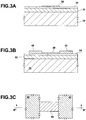
- a substrate 30 e.g., a double-sided polished silicon wafer, having on its surface a selected material or materials, e.g., a layer 32 of low stress silicon nitride, SiN x , and/or a layer 34 of silicon dioxide atop the nitride layer 32.
- the lower layer 32 is SiN x and the upper layer 34 is oxide.
- the lower layer 32 is oxide and the upper layer 34 is SiN x .
- the nitride and/or oxide layers are employed in subsequent steps to form a thinned support structure region in the vicinity of the FET channel region and nanopore location.
- the layered wafer structure can be cleaned by, e.g., oxygen plasma, if desired to render the top surface hydrophilic, or can otherwise be processed to provide a desired surface condition.
- a layer of graphene is then formed on or applied to the top surface of the upper layer, e.g., the oxide layer 34.
- the tape having graphene adhered to it is carefully pressed onto the upper surface 34.
- the tape is then removed, e.g., by dissolving, and the structure washed by solvent, e.g., acetone and IPA.
- solvent e.g., acetone and IPA.
- the graphene can alternatively be deposited on the surface, formed in situ on the surface, or transferred to the surface by an alternative technique.
- the layers 32, 34 provided on the Si substrate are selected in part to enable visualization of a region of graphene disposed on the substrate. Because the refraction of SiN x is about 2, which satisfies the extinction condition on a Si substrate, the maximum contrast between graphene and nitride occurs at zero reflectivity, whereby graphene is invisible on a nitride layer disposed directly on a Si substrate. But if a layer of oxide is provided between the nitride layer and the substrate, graphene is visible on a nitride layer. Therefore, if the upper layer 34 is provided as nitride and the lower layer 32 is provided as oxide, the graphene can be visualized on the nitride surface.
- the oxide layer can be omitted between the nitride layer and the substrate.
- the layer of SiN x can be omitted and only a layer 34 of oxide employed for forming a support structure, or the upper layer can be formed of oxide and the lower layer formed of nitride. It is recognized that SiN x can be particularly well-suited for many applications due to its robust mechanical properties.
- the invention is not limited to a particular support structure material or combination of materials, however. All that is required is a surface on which the presence of graphene can be identified and located. Thus, whatever surface layers are employed, once the graphene is transferred to the surface of the layers, then using optical microscopy, scanning electron microscopy, or other selected technique, regions of graphene are identified and located on the surface for formation of the FET device at that location. Atomic force microscopy can be further employed to identify regions of graphene and measure the thickness of the graphene.
- source and drain regions 40, 42 are then formed in contact with a selected graphene region 36 by, e.g., electron beam lithography, or other suitable process.
- the length of the graphene channel is preferably between about 1 ⁇ m - 2 ⁇ m or less, and preferably can be in the nanometer range.
- the source and drain regions are formed at a location around a graphene region having the corresponding extent, or alternatively, a graphene region is first patterned and etched, in the manner described below, to provide the desired channel length.
- the source and drain regions are formed of a selected electrically conducting or semiconducting material, e.g., a metal such as Ni, Ti/Pd, Pt, or other selected metal, or semiconducting material, such as polysilicon, silicon, or electrically conducting polymer.
- a metal such as Ni, Ti/Pd, Pt, or other selected metal
- semiconducting material such as polysilicon, silicon, or electrically conducting polymer.
- Vapor processes can be employed in the conventional manner to form the source and drain regions. For example, thermal evaporation or other suitable process can be employed for metal deposition.
- the sequence step of source and drain region formation can also be employed to form contact, or bond, pads and connections from the source and drain regions to those bond pads, in the conventional manner for external electrical circuit connection to the source and drain.
- the graphene region in a next process step, can be patterned and etched, if desired, to remove excess graphene such that a selected graphene channel geometry between the source and drain regions is produced.
- a generally rectangular ribbon-shaped or strip-shaped graphene channel region 44 can be preferred. Such is not required, however, and any suitable channel geometry can be employed.
- a graphene channel width that is less than about 1 ⁇ m can be preferred for many applications, and a graphene channel width in the nanometer range is more preferably provided, e.g., between about 10 nm - 25 nm.
- Photolithography with negative photoresist and oxygen plasma etching, or other selected etching process can be employed to pattern and etch a graphene region to produce the selected graphene channel geometry. It can be preferred to record the position of the graphene channel at this process step so that the location of the device can be identified at subsequent back-side process steps.
- a first electrically insulating layer 46 optionally can be provided over the source and drain regions 40, 42, and a second insulating layer 48 can optionally be provided over the entire device, including the graphene channel 44, to reduce the impact of the operating environment on the operational sensing characteristics of the device.
- Both insulating layers can be provided as SiN x , e.g., PECVD SiN x , as an oxide, as a polymer, or other selected insulating material.
- the first insulating layer 46 can be provided with a thickness of, e.g., about 50 nm - 60 nm and the second insulating layer 48 can be provided with a thickness of, e.g., about 20 nm.
- the substrate 30 is bulk-etched to form a membrane 50 on which are supported the source and drain regions 40, 42, and the channel region 44.
- Figs. 3A, 3B , and 3D-3E do not depict the existence of nitride and oxide layers 32, 34 on the backside 52 of the substrate.
- the first steps of forming layers 32, 34 on the surface of the substrate also result in the formation of those layers on the backside of the substrate.
- any such oxide and nitride layers, as well as the silicon bulk are removed.
- both sides of the substrate are coated with a protective layer, e.g., PMMA, in a thickness of, e.g., 250 nm - 300 nm.
- Electron beam lithography is then carried out on the backside of the wafer at the position opposite the graphene FET device to pattern a square or other selected membrane shape.
- a membrane having dimensions of, e.g., 80 ⁇ m ⁇ 80 ⁇ m, or 100 ⁇ m ⁇ 100 ⁇ m, can be employed.
- any oxide and nitride layers on the back side of the wafer are then removed, e.g., with BOE HF and nitride etchants.
- the silicon wafer can then be bulk etched to form the membrane.
- the bulk etching can be carried out by any convenient method, e.g., by plasma etching or other vapor etching, e.g., with XeF 2 , by wet etching, such as with KOH, or with other suitable etching with sufficient selectivity of silicon over nitride, oxide or other surface layer at which the etch will end.
- one or more of the surface layers can be removed, if desired, to form a membrane of a thinner extent.
- an underlying oxide layer can be removed to produce a nitride membrane.
- a self-supported membrane 50 that is supported at its edges by the substrate 30.
- the FET device is positioned on the membrane.
- These connections and bond pads are formed at the time of source and drain region formation as described above.
- a portion of the FET device elements and circuitry can be disposed on the membrane with other of the elements disposed on the substrate at locations distant from the membrane. There is not specific requirement for the location of the device elements on or off the membrane. All that is required is a relatively thin support region at the location intended for the nanopore of the FET device.
- a 100 ⁇ m ⁇ 100 ⁇ m membrane can be formed with 20 or more FET devices on the membrane to accommodate simultaneous and parallel molecular sensing, as described below.
- the thickness of the surface layer or layers 32, 34 sets the thickness of the membrane. These layers are therefore preferably tailored in thickness at the time of their deposition to set the desired membrane thickness and correspondingly, to set the length of the nanopore section that traverses the membrane. For many applications, it can be preferred to select an oxide layer thickness that enables visualization of graphene and then to set a nitride layer thickness, if employed, to provide adequate mechanical support while also accommodating a selected nanopore formation process. In general, a relatively thinner membrane is preferred because the membrane thickness directly affects the voltage required for translocation.
- membranes can be employed, e.g., SiN x TEM grid membranes having a thickness of, e.g., about 30 nm, can be employed.
- SiN x TEM grid membranes having a thickness of, e.g., about 30 nm, can be employed.
- the process described above, in which graphene is formed on a structure and then the structure thinned to form a membrane can be preferred.
- the invention is not limited to membrane structures for the geometry of a support in the vicinity of the FET channel. Plates, cantilevers, bridges, trusses, substrates, or other suitable configuration can be employed for the support at the location of the FET channel.
- a nanopore is formed at a selected location relative to the graphene channel region.
- the cross sectional view of Fig. 3F is taken at the cross section shown in the planar view of Fig. 3C .
- the nanopore is provided with an extent corresponding to a molecule, molecular component, or other species of interest.
- the nanopore be less than 1000 nm in diameter, preferably less than 100 nm.
- a nanopore diameter less than about 10 nm or less than about 5 nm is preferred, with a diameter of between about 1.5 nm and about 2 nm preferred for ssDNA sensing.
- the invention is not limited to a particular nanopore diameter and instead requires that the diameter provide adequate extent for a molecule or other species of interest.
- the nanopore diameter is comparable to the extent of a molecular component, e.g., a DNA base, any geometric differences between bases can result in differing translocation duration, aiding in circuit parameter analysis for discrimination of specific DNA bases.
- the whole substrate arrangement is loaded into a TEM specimen chamber and the graphene FET device is located and identified under the TEM. Then a high energy electron beam is focused into a 1-2 nm beam spot at the desired location of the nanopore, e.g., at a point centrally along the graphene channel region, at the edge of the channel region, or just adjacent to the channel region, and a nanometer-sized hole is punched through the graphene layer and the underlying oxide/SiN x membrane. It is preferred to direct the electron beam to the backside 56 of the membrane in formation of the nanopore. This eliminates exposure of the insulating layers 46, 48, to the electron beam and the unwanted electrical charging of those layers that could result.
- a nanopore of a selected diameter can be formed through the membranes in a matter of seconds to minutes.
- the size of the nanopore can be controlled by choice of the condenser aperture, illumination time, and other beam characteristics.
- the FET device can be annealed after the nanopore formation to improve electrical characteristics of the device and in particular the channel region.
- the high-energy electron beam can introduce a potential barrier around the nanopore and therefore decrease the channel region conductance.
- an optional thermal anneal can be performed to improve the conductance of the channel region.
- a functional graphene-based FET molecular sensor is completed and ready for connection in a circuit and an environment of molecules or other species to be sensed.
- the channel region 44 of the FET device is sandwiched between the membrane surface layer 34, e.g., nitride, and an upper insulating layer 48.
- the membrane surface layer 34 e.g., nitride
- an upper insulating layer 48 e.g., nitride
- Molecule-channel interaction can therefore take place only along the extent of the walls of the nanopore, through the thickness of the channel, e.g., through the thickness of a graphene layer.
- the zone of molecular sensing is constrained to the extent of the nanopore through the channel region material, and therefore that the channel region layer thickness can indeed set the spatial extent of molecular interaction with the FET sensor.
- Single-molecule or single-molecular component sensing or other selected limited molecular sensing accordingly can be enforced.
- the nanopore walls i.e., the cross-sectional nanopore edge 56
- the nanopore walls can be provided on its surface with reaction entities or other species, e.g., binding partners, that are specific for a moiety of interest to be sensed, or reacted with.
- the nanopore periphery through the thickness of the channel region can be functionalized with a selected species.
- Such functionalization results in FET behavior that is indicative of reaction between the functionalization species and a corresponding moiety or interest present in the environment of molecules to be sensed.
- Provision of a functionalization species at the nanopore can be carried out in the manner described in U.S. Patent Application Publication US2002/0117659, published August 29, 2002 , the entirety of which is hereby incorporated by reference.
- the channel region material layer can be formed of any suitable material, layers of material, or composite layers of multiple materials, that meets the requirement of conductance as an FET channel, that can be etched to form a nanopore there-through, and that can be provided in a thickness corresponding to a selected molecule or molecular component to be sensed. Silicon, polysilicon, or other IV-VI material, III-V materials, conductive polymers, and other microelectronic materials can be employed as channel materials.
- Such can be provided by, e.g., SOI wafers, by epitaxial deposition or other vapor formation process, by evaporation, sputtering, CVD or other suitable process that enables the formation of a selected channel region material.
- the channel region material can be thinned to the desired thickness corresponding to a molecule to be sensed, such that single or near-single molecule sensing resolution is attained.
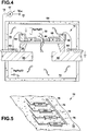
- the nanopore FET device 10 is bonded to, e.g., a PCB chip carrier 60.
- the source and drain contact pads 54, 56 are connected to connector pads 62, 64 by conventional wire bonding or other suitable technique.
- Preferably all bonding wires and contact pads are passivated with, e.g., SiN x or HfO 2 , in the manner described above or with another passivation layer 68.
- the device 10 and chip carrier 60 are enclosed in a chamber, e.g., a PDMS chamber 64 which forms with the front side of the device a supply reservoir 70 for supplying a solution of interest to be analyzed, and which forms with the back side of the device a collection reservoir 72 for collecting a solution after it has been analyzed.
- a chamber e.g., a PDMS chamber 64 which forms with the front side of the device a supply reservoir 70 for supplying a solution of interest to be analyzed, and which forms with the back side of the device a collection reservoir 72 for collecting a solution after it has been analyzed.
- a chamber e.g., a PDMS chamber 64 which forms with the front side of the device a supply reservoir 70 for supplying a solution of interest to be analyzed, and which forms with the back side of the device a collection reservoir 72 for collecting a solution after it has been analyzed.
- These reservoir functions can be reversed if desired.
- the sealed mating of the substrate 30 with the circuit board 60
- Molecules of interest are provided in the solution to be analyzed by translocation through the nanopore.
- Other example molecules to be analyzed include, in general, biomolecules, such as ssDNA, dsDNA or RNA strands, oligonucleotides, or nucleic acids in general, such as proteins, and other biomolecules.
- Non-biological molecules, and indeed, any non-molecular species can also be analyzed as-desired, if such can be supplied for translocation through the nanopore.
- a driving force is imposed across the nanopore between the two reservoir solutions, to cause translocation of species in the supply reservoir through the nanopore and into the collection reservoir.
- Ag/AgCl electrodes, or other electrodes can be used to apply a voltage difference across the nanopore.
- gate electrodes defined on the chip carrier can be used to apply solution potentials.
- No particular driving force is required by the invention; the translocation of species through the nanopore for analysis is all that is required.
- it can be preferably to rinse the reservoirs with ethanol and DI water before introduction of a solution of interest. Further, it can be preferred to operate the system inside, e.g., a Faraday box to eliminate external noise.
- a source-drain bias voltage source V SD
- at least one circuit parameter measurement device e.g., a current amplifier 17.
- the charge and dipoles of the DNA or other molecules or molecular components cause a change in conductance of the channel region 44 that is directly attributable to the one or more molecules or molecular components in the nanopore at a given time.
- the FET circuit parameters correspondingly change as a result of the conductance change due to molecular translocation, and are sensed by the current amplifier or other device or system.
- multiple FET devices can be fabricated on a single support substrate, e.g., on a membrane.
- This configuration enables parallel, simultaneous sensing operations by multiple FET devices provided in communication with a common reservoir.
- a molecular sensing array 75 of FET devices configured for parallel molecular analysis of a sample solution.
- Each device 76 in the array 75 can be configured to operate for translocation of molecules through a nanopore in the channel region or adjacent to the channel region of the device.
- the FET molecular sensor of the invention enables superior resolution and sensitivity for the detection and analysis of molecules and molecular components.
- the resolution of the detection can be made as low as a single DNA base by employing an FET channel region material having a thickness that corresponds to the extent of a DNA base.
- Graphene is therefore particularly well-suited as a channel region material.
- the superior electrical characteristics of graphene, along with its inherent thinness, enable a graphene nanopore FET sensor to achieve molecular sensing, and gene sequencing, at very high resolution and sensitivity.
Applications Claiming Priority (3)
| Application Number | Priority Date | Filing Date | Title |
|---|---|---|---|
| US99338807P | 2007-09-12 | 2007-09-12 | |
| EP08830263.3A EP2195648B1 (fr) | 2007-09-12 | 2008-09-12 | Capteur moléculaire haute résolution en graphine avec ouverture dans la couche de graphene |
| PCT/US2008/010637 WO2009035647A1 (fr) | 2007-09-12 | 2008-09-12 | Capteur moléculaire haute résolution en feuille de carbone avec ouverture dans la couche de feuille de carbone |
Related Parent Applications (1)
| Application Number | Title | Priority Date | Filing Date |
|---|---|---|---|
| EP08830263.3A Division EP2195648B1 (fr) | 2007-09-12 | 2008-09-12 | Capteur moléculaire haute résolution en graphine avec ouverture dans la couche de graphene |
Publications (3)
| Publication Number | Publication Date |
|---|---|
| EP3540436A1 true EP3540436A1 (fr) | 2019-09-18 |
| EP3540436B1 EP3540436B1 (fr) | 2023-11-01 |
| EP3540436C0 EP3540436C0 (fr) | 2023-11-01 |
Family
ID=40032526
Family Applications (2)
| Application Number | Title | Priority Date | Filing Date |
|---|---|---|---|
| EP08830263.3A Active EP2195648B1 (fr) | 2007-09-12 | 2008-09-12 | Capteur moléculaire haute résolution en graphine avec ouverture dans la couche de graphene |
| EP19172912.8A Active EP3540436B1 (fr) | 2007-09-12 | 2008-09-12 | Capteur moléculaire haute résolution |
Family Applications Before (1)
| Application Number | Title | Priority Date | Filing Date |
|---|---|---|---|
| EP08830263.3A Active EP2195648B1 (fr) | 2007-09-12 | 2008-09-12 | Capteur moléculaire haute résolution en graphine avec ouverture dans la couche de graphene |
Country Status (3)
| Country | Link |
|---|---|
| US (2) | US8698481B2 (fr) |
| EP (2) | EP2195648B1 (fr) |
| WO (1) | WO2009035647A1 (fr) |
Families Citing this family (273)
| Publication number | Priority date | Publication date | Assignee | Title |
|---|---|---|---|---|
| US20120160687A1 (en) | 1995-03-17 | 2012-06-28 | President And Fellows Of Harvard College | Characterization of individual polymer molecules based on monomer-interface interactions |
| WO2005017025A2 (fr) | 2003-08-15 | 2005-02-24 | The President And Fellows Of Harvard College | Etude de molecules de polymere et conformations avec un nanopore |
| DK2122344T3 (da) | 2007-02-20 | 2019-07-15 | Oxford Nanopore Tech Ltd | Lipiddobbeltlags-sensorsystem |
| US20110005918A1 (en) | 2007-04-04 | 2011-01-13 | Akeson Mark A | Compositions, devices, systems, and methods for using a nanopore |
| GB0724736D0 (en) | 2007-12-19 | 2008-01-30 | Oxford Nanolabs Ltd | Formation of layers of amphiphilic molecules |
| CN103695530B (zh) | 2008-07-07 | 2016-05-25 | 牛津纳米孔技术有限公司 | 酶-孔构建体 |
| CA2750879C (fr) | 2009-01-30 | 2018-05-22 | Oxford Nanopore Technologies Limited | Adaptateurs pour des constructions d'acide nucleique dans le sequencage de sequences transmembranaires |
| US8441361B2 (en) | 2010-02-13 | 2013-05-14 | Mcallister Technologies, Llc | Methods and apparatuses for detection of properties of fluid conveyance systems |
| US8312759B2 (en) * | 2009-02-17 | 2012-11-20 | Mcalister Technologies, Llc | Methods, devices, and systems for detecting properties of target samples |
| US9035281B2 (en) * | 2009-06-30 | 2015-05-19 | Nokia Technologies Oy | Graphene device and method of fabricating a graphene device |
| GB2471672B (en) * | 2009-07-07 | 2015-12-09 | Swansea Innovations Ltd | Graphene biosensor |
| AU2010307229B2 (en) * | 2009-09-18 | 2016-02-25 | President And Fellows Of Harvard College | Bare single-layer graphene membrane having a nanopore enabling high-sensitivity molecular detection and analysis |
| CN101694474B (zh) * | 2009-10-22 | 2012-10-10 | 浙江大学 | 一种纳米孔电学传感器 |
| JP5697069B2 (ja) * | 2009-11-30 | 2015-04-08 | 独立行政法人物質・材料研究機構 | グラフェントランジスタ |
| US9605307B2 (en) | 2010-02-08 | 2017-03-28 | Genia Technologies, Inc. | Systems and methods for forming a nanopore in a lipid bilayer |
| US9121823B2 (en) * | 2010-02-19 | 2015-09-01 | The Trustees Of The University Of Pennsylvania | High-resolution analysis devices and related methods |
| US8603303B2 (en) | 2010-03-15 | 2013-12-10 | International Business Machines Corporation | Nanopore based device for cutting long DNA molecules into fragments |
| US8890277B2 (en) | 2010-03-15 | 2014-11-18 | University Of Florida Research Foundation Inc. | Graphite and/or graphene semiconductor devices |
| US9146209B2 (en) * | 2010-03-30 | 2015-09-29 | The Trustees Of The University Of Pennsylvania | DNA-decorated graphene chemical sensors |
| US8828138B2 (en) * | 2010-05-17 | 2014-09-09 | International Business Machines Corporation | FET nanopore sensor |
| CN103154729B (zh) * | 2010-06-08 | 2015-01-07 | 哈佛大学校长及研究员协会 | 具有由石墨烯支持的人工脂质膜的纳米孔装置 |
| KR101209000B1 (ko) | 2010-06-25 | 2012-12-06 | 서울대학교산학협력단 | 그래핀 나노 포어 구조를 이용한 이온 소자 및 dna 분석용 장치 |
| US9475709B2 (en) | 2010-08-25 | 2016-10-25 | Lockheed Martin Corporation | Perforated graphene deionization or desalination |
| US20140051068A1 (en) | 2010-09-07 | 2014-02-20 | The Regents Of The University Of California | Control of dna movement in a nanopore at one nucleotide precision by a processive enzyme |
| US8395774B2 (en) * | 2010-09-21 | 2013-03-12 | International Business Machines Corporation | Graphene optical sensor |
| EP2623960B1 (fr) | 2010-09-29 | 2020-11-11 | Hitachi High-Tech Corporation | Dispositif et procédé d'analyse optique de biopolymère |
| CN101986145B (zh) * | 2010-09-30 | 2012-11-21 | 浙江大学 | 一种纳米孔电学传感器 |
| CN102095768B (zh) | 2010-11-16 | 2014-07-09 | 浙江大学 | 一种亚纳米厚度的纳米孔传感器 |
| GB2485559A (en) * | 2010-11-18 | 2012-05-23 | Univ Plymouth | Graphene based electronic device |
| KR101715355B1 (ko) | 2010-11-30 | 2017-03-13 | 삼성전자주식회사 | 그래핀 전자 소자 |
| EP2649217A4 (fr) * | 2010-12-08 | 2014-11-26 | 3M Innovative Properties Co | Article et procédé de fabrication et d'utilisation de celui-ci |
| US20120146162A1 (en) * | 2010-12-13 | 2012-06-14 | Samsung Electronics Co., Ltd. | Nanosensor and method of manufacturing the same |
| CN102538617A (zh) * | 2010-12-31 | 2012-07-04 | 上海和达汽车配件有限公司 | 一种检测汽车中部支架总成的检具 |
| US20120193231A1 (en) | 2011-01-28 | 2012-08-02 | International Business Machines Corporation | Dna sequencing using multiple metal layer structure with organic coatings forming transient bonding to dna bases |
| US8986524B2 (en) | 2011-01-28 | 2015-03-24 | International Business Machines Corporation | DNA sequence using multiple metal layer structure with different organic coatings forming different transient bondings to DNA |
| US8852407B2 (en) | 2011-01-28 | 2014-10-07 | International Business Machines Corporation | Electron beam sculpting of tunneling junction for nanopore DNA sequencing |
| WO2012107778A2 (fr) | 2011-02-11 | 2012-08-16 | Oxford Nanopore Technologies Limited | Pores mutants |
| US9859063B2 (en) | 2011-02-13 | 2018-01-02 | Indiana University Research & Technology Corporation | High surface area nano-structured graphene composites and capacitive devices incorporating the same |
| WO2012109665A1 (fr) * | 2011-02-13 | 2012-08-16 | Indiana University Research And Technology Corporation | Composites de graphène nano-structurés à surface élevée et dispositifs capacitifs les intégrant |
| US9656862B2 (en) | 2011-02-13 | 2017-05-23 | Indiana University Research And Technology Corporation | High surface area nano-structured graphene composites and capacitive devices incorporating the same |
| US9599614B2 (en) * | 2011-03-14 | 2017-03-21 | Yale University | Calibration of nanostructure sensors |
| BR112013023586B1 (pt) | 2011-03-15 | 2021-01-26 | President And Fellows Of Harvard College | método de formação de um nanoporo em um material nanométrico e estrutura nanométrica |
| CN103842519B (zh) * | 2011-04-04 | 2018-02-06 | 哈佛大学校长及研究员协会 | 通过局部电位测量进行的纳米孔感测 |
| US20130307029A1 (en) * | 2011-04-19 | 2013-11-21 | Mingsheng Xu | High-Resolution Biosensor |
| US8518829B2 (en) * | 2011-04-22 | 2013-08-27 | International Business Machines Corporation | Self-sealed fluidic channels for nanopore array |
| JP6480183B2 (ja) | 2011-05-27 | 2019-03-06 | オックスフォード ナノポール テクノロジーズ リミテッド | 結合方法 |
| WO2012165400A1 (fr) | 2011-06-03 | 2012-12-06 | 株式会社日立ハイテクノロジーズ | Procédé et dispositif d'analyse optique d'un biopolymère |
| KR101910978B1 (ko) * | 2011-06-22 | 2018-10-24 | 삼성전자주식회사 | 나노 센서 및 그의 제조 방법 |
| KR20130001614A (ko) * | 2011-06-27 | 2013-01-04 | 삼성전자주식회사 | 나노 센서 및 이를 사용하는 표적 분자의 검출 방법 |
| US10761043B2 (en) | 2011-07-22 | 2020-09-01 | The Trustees Of The University Of Pennsylvania | Graphene-based nanopore and nanostructure devices and methods for macromolecular analysis |
| AU2012288629B2 (en) | 2011-07-25 | 2017-02-02 | Oxford Nanopore Technologies Limited | Hairpin loop method for double strand polynucleotide sequencing using transmembrane pores |
| EP2737536B1 (fr) | 2011-07-27 | 2018-05-09 | The Board of Trustees of the University of Illionis | Capteurs à nanopore pour la caractérisation biomoléculaire |
| CN102411019B (zh) * | 2011-08-08 | 2014-02-19 | 北京大学 | 一种基于石墨烯电极的分子器件用于检测有机生物小分子的方法 |
| JP5670278B2 (ja) * | 2011-08-09 | 2015-02-18 | 株式会社日立ハイテクノロジーズ | ナノポア式分析装置 |
| KR101353055B1 (ko) * | 2011-08-17 | 2014-01-17 | 서울대학교산학협력단 | 절연성 지지 부재 상의 나노 포어 구조를 이용한 이온 소자 |
| US8759153B2 (en) * | 2011-09-06 | 2014-06-24 | Infineon Technologies Ag | Method for making a sensor device using a graphene layer |
| US9090936B2 (en) | 2011-09-19 | 2015-07-28 | California Institute Of Technology | Using a field effect device for identifying translocating charge-tagged molecules in a nanopore sequencing device |
| US9753001B1 (en) | 2011-09-23 | 2017-09-05 | The United States Of America As Represented By The Administrator Of National Aeronautics And Space Administration | Polymer nanofiber based reversible nano-switch/sensor diode (nanoSSSD) device |
| US9016108B1 (en) | 2011-09-23 | 2015-04-28 | The United States Of America As Represented By The Administrator Of National Aeronautics And Space Administration | Graphene based reversible nano-switch/sensor Schottky diode (nanoSSSD) device |
| WO2013041878A1 (fr) | 2011-09-23 | 2013-03-28 | Oxford Nanopore Technologies Limited | Analyse d'un polymère comprenant des unités de polymère |
| EP2574923A1 (fr) * | 2011-09-28 | 2013-04-03 | Koninklijke Philips Electronics N.V. | Appareil pour le traitement de molécules uniques |
| KR20140090633A (ko) | 2011-10-21 | 2014-07-17 | 옥스포드 나노포어 테크놀로지즈 리미티드 | 포어 및 hel308 헬리카제를 사용하여 표적 폴리뉴클레오티드를 특성화하는 방법 |
| CN102506693A (zh) * | 2011-11-04 | 2012-06-20 | 南京航空航天大学 | 一种石墨烯应变测量和运动传感装置及其制法 |
| US20130186758A1 (en) * | 2011-12-09 | 2013-07-25 | University Of Delaware | Current-carrying nanowire having a nanopore for high-sensitivity detection and analysis of biomolecules |
| WO2013096404A1 (fr) * | 2011-12-22 | 2013-06-27 | Becton, Dickinson And Company | Procédés et appareil pour la détection rapide de microorganismes infectieux |
| CN104136631B (zh) | 2011-12-29 | 2017-03-01 | 牛津纳米孔技术公司 | 使用xpd解旋酶表征多核苷酸的方法 |
| WO2013098562A2 (fr) | 2011-12-29 | 2013-07-04 | Oxford Nanopore Technologies Limited | Procédé enzymatique |
| JP5898969B2 (ja) * | 2012-01-18 | 2016-04-06 | 株式会社日立製作所 | 半導体装置 |
| GB201202519D0 (en) | 2012-02-13 | 2012-03-28 | Oxford Nanopore Tech Ltd | Apparatus for supporting an array of layers of amphiphilic molecules and method of forming an array of layers of amphiphilic molecules |
| AU2013220156B2 (en) | 2012-02-15 | 2018-08-09 | Oxford Nanopore Technologies Limited | Aptamer method |
| CN104321441B (zh) | 2012-02-16 | 2016-10-19 | 牛津楠路珀尔科技有限公司 | 聚合物的测量的分析 |
| US9028663B2 (en) * | 2012-03-21 | 2015-05-12 | Lockheed Martin Corporation | Molecular separation device |
| EP2642341A2 (fr) | 2012-03-22 | 2013-09-25 | Koninklijke Philips N.V. | Méthode de fabrication d'un dispositif pour le traitement de molécules individuelles |
| US9095823B2 (en) * | 2012-03-29 | 2015-08-04 | Lockheed Martin Corporation | Tunable layered membrane configuration for filtration and selective isolation and recovery devices |
| US20130256139A1 (en) * | 2012-03-30 | 2013-10-03 | International Business Machines Corporation | Functionalized graphene or graphene oxide nanopore for bio-molecular sensing and dna sequencing |
| US10029915B2 (en) | 2012-04-04 | 2018-07-24 | International Business Machines Corporation | Functionally switchable self-assembled coating compound for controlling translocation of molecule through nanopores |
| KR101906967B1 (ko) | 2012-04-05 | 2018-10-11 | 삼성전자주식회사 | 나노갭 센서 및 이의 제조 방법 |
| KR20130114435A (ko) * | 2012-04-09 | 2013-10-17 | 삼성전자주식회사 | 다수의 전극을 갖는 생분자 검출 장치 |
| BR112014025157B1 (pt) | 2012-04-10 | 2022-02-08 | Oxford Nanopore Technologies Limited | Monômero de lisenina mutante, construto, poro, método para caracterizar um analito alvo, uso de um poro, e, kit |
| US9758821B2 (en) * | 2012-04-17 | 2017-09-12 | International Business Machines Corporation | Graphene transistor gated by charges through a nanopore for bio-molecular sensing and DNA sequencing |
| KR101600132B1 (ko) * | 2012-04-20 | 2016-03-04 | 나노칩스 (주) | 적층 나노리본을 이용한 실시간 분자서열 분석시스템 및 분석방법 |
| US9067811B1 (en) | 2012-05-25 | 2015-06-30 | Lockheed Martin Corporation | System, method, and control for graphenoid desalination |
| US10376845B2 (en) | 2016-04-14 | 2019-08-13 | Lockheed Martin Corporation | Membranes with tunable selectivity |
| US9744617B2 (en) | 2014-01-31 | 2017-08-29 | Lockheed Martin Corporation | Methods for perforating multi-layer graphene through ion bombardment |
| US9610546B2 (en) | 2014-03-12 | 2017-04-04 | Lockheed Martin Corporation | Separation membranes formed from perforated graphene and methods for use thereof |
| US10653824B2 (en) | 2012-05-25 | 2020-05-19 | Lockheed Martin Corporation | Two-dimensional materials and uses thereof |
| US10118130B2 (en) | 2016-04-14 | 2018-11-06 | Lockheed Martin Corporation | Two-dimensional membrane structures having flow passages |
| US9834809B2 (en) | 2014-02-28 | 2017-12-05 | Lockheed Martin Corporation | Syringe for obtaining nano-sized materials for selective assays and related methods of use |
| US10980919B2 (en) | 2016-04-14 | 2021-04-20 | Lockheed Martin Corporation | Methods for in vivo and in vitro use of graphene and other two-dimensional materials |
| CN102788824B (zh) * | 2012-06-06 | 2014-07-02 | 河南赛沃思生物科技有限公司 | 一种dna生物传感器的制备方法 |
| US9136160B2 (en) * | 2012-06-29 | 2015-09-15 | Institute of Microelectronics, Chinese Academy of Sciences | Solid hole array and method for forming the same |
| KR101910976B1 (ko) | 2012-07-16 | 2018-10-23 | 삼성전자주식회사 | 그래핀을 이용한 전계효과 트랜지스터 |
| JP6429773B2 (ja) | 2012-07-19 | 2018-11-28 | オックスフォード ナノポール テクノロジーズ リミテッド | 酵素構築物 |
| WO2014013259A1 (fr) | 2012-07-19 | 2014-01-23 | Oxford Nanopore Technologies Limited | Procédé ssb |
| JP6614972B2 (ja) | 2012-07-19 | 2019-12-04 | オックスフォード ナノポール テクノロジーズ リミテッド | 修飾ヘリカーゼ |
| JP6033602B2 (ja) * | 2012-08-08 | 2016-11-30 | 株式会社日立ハイテクノロジーズ | 生体分子検出方法、生体分子検出装置、および分析用デバイス |
| KR20140028602A (ko) * | 2012-08-29 | 2014-03-10 | 삼성전자주식회사 | 그래핀을 포함하는 나노 센서 및 이의 제조 방법 |
| KR101984695B1 (ko) * | 2012-08-29 | 2019-09-03 | 삼성전자주식회사 | 그래핀 소자 및 그 제조방법 |
| US9551023B2 (en) | 2012-09-14 | 2017-01-24 | Oxford Nanopore Technologies Ltd. | Sample preparation method |
| WO2014052616A2 (fr) | 2012-09-27 | 2014-04-03 | The Trustees Of The University Of Pennsylvania | Dispositifs nanoporeux à nanoélectrode isolée et procédés connexes |
| GB201313121D0 (en) | 2013-07-23 | 2013-09-04 | Oxford Nanopore Tech Ltd | Array of volumes of polar medium |
| KR101927415B1 (ko) * | 2012-11-05 | 2019-03-07 | 삼성전자주식회사 | 나노갭 소자 및 이로부터의 신호를 처리하는 방법 |
| WO2014072703A1 (fr) | 2012-11-06 | 2014-05-15 | Oxford Nanopore Technologies Limited | Procédé quadruplex |
| US20150273401A1 (en) * | 2012-11-30 | 2015-10-01 | Empire Technology Development Llc | Selective membrane supported on nanoporous graphene |
| WO2014084860A1 (fr) | 2012-11-30 | 2014-06-05 | Empire Technology Development, Llc | Membrane de graphène stratifiée sur un support tissé ou non tissé poreux |
| GB201222928D0 (en) | 2012-12-19 | 2013-01-30 | Oxford Nanopore Tech Ltd | Analysis of a polynucleotide |
| EP2755022B1 (fr) | 2013-01-15 | 2018-05-30 | Honeywell International Inc. | Nanocapteur |
| US10847251B2 (en) | 2013-01-17 | 2020-11-24 | Illumina, Inc. | Genomic infrastructure for on-site or cloud-based DNA and RNA processing and analysis |
| US9679104B2 (en) | 2013-01-17 | 2017-06-13 | Edico Genome, Corp. | Bioinformatics systems, apparatuses, and methods executed on an integrated circuit processing platform |
| US9792405B2 (en) | 2013-01-17 | 2017-10-17 | Edico Genome, Corp. | Bioinformatics systems, apparatuses, and methods executed on an integrated circuit processing platform |
| US10068054B2 (en) | 2013-01-17 | 2018-09-04 | Edico Genome, Corp. | Bioinformatics systems, apparatuses, and methods executed on an integrated circuit processing platform |
| US10691775B2 (en) | 2013-01-17 | 2020-06-23 | Edico Genome, Corp. | Bioinformatics systems, apparatuses, and methods executed on an integrated circuit processing platform |
| DE112013000972T5 (de) * | 2013-02-26 | 2014-11-06 | Hitachi, Ltd. | FET-Array-Substrat, Analysesystem und Analyseverfahren |
| SG11201507138RA (en) | 2013-03-08 | 2015-10-29 | Oxford Nanopore Tech Ltd | Enzyme stalling method |
| GB201314695D0 (en) | 2013-08-16 | 2013-10-02 | Oxford Nanopore Tech Ltd | Method |
| GB201318465D0 (en) | 2013-10-18 | 2013-12-04 | Oxford Nanopore Tech Ltd | Method |
| TW201504140A (zh) | 2013-03-12 | 2015-02-01 | Lockheed Corp | 形成具有均勻孔尺寸之多孔石墨烯之方法 |
| CN105102105A (zh) | 2013-03-13 | 2015-11-25 | 洛克希德马丁公司 | 纳米多孔薄膜及其制造方法 |
| US9678036B2 (en) * | 2013-03-15 | 2017-06-13 | The Regents Of The University Of California | Graphene-based gas and bio sensor with high sensitivity and selectivity |
| GB201313477D0 (en) | 2013-07-29 | 2013-09-11 | Univ Leuven Kath | Nanopore biosensors for detection of proteins and nucleic acids |
| US9250206B2 (en) | 2013-04-04 | 2016-02-02 | International Business Machines Corporation | Controlled translocation of macromolecules employing a funnel nanopore structure and a gel |
| US9046511B2 (en) | 2013-04-18 | 2015-06-02 | International Business Machines Corporation | Fabrication of tunneling junction for nanopore DNA sequencing |
| US10677752B2 (en) | 2013-04-18 | 2020-06-09 | The Board Of Trustees Of The University Of Illinois | Method and apparatus analyzing a target material |
| US10345289B2 (en) * | 2013-04-18 | 2019-07-09 | The Board Of Trustees Of The University Of Illinois | Method and apparatus for analyzing a target material |
| US8890121B1 (en) * | 2013-05-06 | 2014-11-18 | International Business Machines Corporation | Integrated nanowire/nanosheet nanogap and nanopore for DNA and RNA sequencing |
| US9188578B2 (en) * | 2013-06-19 | 2015-11-17 | Globalfoundries Inc. | Nanogap device with capped nanowire structures |
| US9182369B2 (en) | 2013-06-19 | 2015-11-10 | Globalfoundries Inc. | Manufacturable sub-3 nanometer palladium gap devices for fixed electrode tunneling recognition |
| US9572918B2 (en) | 2013-06-21 | 2017-02-21 | Lockheed Martin Corporation | Graphene-based filter for isolating a substance from blood |
| US10030266B2 (en) * | 2013-06-27 | 2018-07-24 | Hitachi, Ltd. | Semiconductor device and manufacturing method thereof |
| US9377431B2 (en) * | 2013-07-24 | 2016-06-28 | Globalfoundries Inc. | Heterojunction nanopore for sequencing |
| US9683937B2 (en) | 2013-08-23 | 2017-06-20 | Semiconductor Components Industries, Llc | Imaging devices for molecule detection |
| EP2848929A1 (fr) | 2013-09-11 | 2015-03-18 | AIT Austrian Institute of Technology GmbH | Biocapteur à base de transistors à effet de graphène |
| KR102144995B1 (ko) | 2013-09-12 | 2020-08-14 | 삼성전자주식회사 | 그래핀 나노포어를 포함하는 나노포어 소자 및 그 제조 방법 |
| GB201406151D0 (en) | 2014-04-04 | 2014-05-21 | Oxford Nanopore Tech Ltd | Method |
| CA2927726A1 (fr) | 2013-10-18 | 2015-04-23 | Oxford Nanopore Technologies Limited | Heliscases modifiees a utiliser dans le sequencement d'acide nucleique |
| US20160282326A1 (en) * | 2013-11-25 | 2016-09-29 | Northeastern University | Freestanding Ultrathin Membranes and Transfer-Free Fabrication Thereof |
| GB201322399D0 (en) * | 2013-12-18 | 2014-02-05 | Lancaster University | Sensor assembly |
| JP6749243B2 (ja) | 2014-01-22 | 2020-09-02 | オックスフォード ナノポール テクノロジーズ リミテッド | 1つまたは複数のポリヌクレオチド結合タンパク質を標的ポリヌクレオチドに付着させる方法 |
| GB201406155D0 (en) | 2014-04-04 | 2014-05-21 | Oxford Nanopore Tech Ltd | Method |
| WO2015116946A1 (fr) | 2014-01-31 | 2015-08-06 | Lockheed Martin Corporation | Perforation de matériaux bidimensionnels à l'aide d'un large champ ionique |
| KR20160142282A (ko) | 2014-01-31 | 2016-12-12 | 록히드 마틴 코포레이션 | 다공성 비-희생 지지층을 사용하여 2차원 물질로 복합 구조를 형성하기 위한 프로세스 |
| EP3108229A4 (fr) | 2014-02-19 | 2017-09-06 | University of Washington | Analyse de caractéristiques de protéines basée sur les nanopores |
| GB201403096D0 (en) | 2014-02-21 | 2014-04-09 | Oxford Nanopore Tech Ltd | Sample preparation method |
| CA2942496A1 (fr) | 2014-03-12 | 2015-09-17 | Lockheed Martin Corporation | Membranes de separation formees a partir de graphene perfore |
| US10020500B2 (en) | 2014-03-25 | 2018-07-10 | Indiana University Research And Technology Corporation | Carbonized polyaniline-grafted silicon nanoparticles encapsulated in graphene sheets for li-ion battery anodes |
| WO2015150786A1 (fr) | 2014-04-04 | 2015-10-08 | Oxford Nanopore Technologies Limited | Méthode de caractérisation d'un acide nucléique double brin au moyen d'un nano-pore et de molécules d'ancrage aux deux extrémités dudit acide nucléique |
| CN104212711B (zh) * | 2014-04-08 | 2017-10-27 | 上海小海龟科技有限公司 | 电子传感器及基于电子传感器的基因探测方法 |
| US20160054312A1 (en) | 2014-04-28 | 2016-02-25 | Nanomedical Diagnostics, Inc. | Chemically differentiated sensor array |
| US9765395B2 (en) * | 2014-04-28 | 2017-09-19 | Nanomedical Diagnostics, Inc. | System and method for DNA sequencing and blood chemistry analysis |
| US11215580B2 (en) | 2014-04-28 | 2022-01-04 | Cardea Bio, Inc. | System and method for DNA sequencing and blood chemistry analysis |
| US9618476B2 (en) | 2014-04-28 | 2017-04-11 | Nanomedical Diagnostics, Inc. | System and method for electronic biological sample analysis |
| US10443097B2 (en) | 2014-05-02 | 2019-10-15 | Oxford Nanopore Technologies Ltd. | Method of improving the movement of a target polynucleotide with respect to a transmembrane pore |
| GB201417712D0 (en) | 2014-10-07 | 2014-11-19 | Oxford Nanopore Tech Ltd | Method |
| CN103995035A (zh) * | 2014-05-29 | 2014-08-20 | 东南大学 | 用于碱基序列检测的多栅极石墨烯场效应管结构及制备方法 |
| US9423345B2 (en) | 2014-06-24 | 2016-08-23 | International Business Machines Corporation | Chemical sensors based on plasmon resonance in graphene |
| CN117164682A (zh) | 2014-09-01 | 2023-12-05 | 弗拉芒区生物技术研究所 | 突变csgg孔 |
| JP2017534311A (ja) | 2014-09-02 | 2017-11-24 | ロッキード・マーチン・コーポレーション | 二次元膜材料をベースとする血液透析膜および血液濾過膜、ならびにそれを用いた方法 |
| EP3204511B1 (fr) | 2014-10-07 | 2021-07-28 | Oxford Nanopore Technologies Limited | Pores mutants |
| GB201418159D0 (en) | 2014-10-14 | 2014-11-26 | Oxford Nanopore Tech Ltd | Method |
| US10689697B2 (en) | 2014-10-16 | 2020-06-23 | Oxford Nanopore Technologies Ltd. | Analysis of a polymer |
| GB201418469D0 (en) | 2014-10-17 | 2014-12-03 | Oxford Nanopore Tech Ltd | Method |
| GB201418512D0 (en) | 2014-10-17 | 2014-12-03 | Oxford Nanopore Tech Ltd | Electrical device with detachable components |
| US11782057B2 (en) | 2014-12-18 | 2023-10-10 | Cardea Bio, Inc. | Ic with graphene fet sensor array patterned in layers above circuitry formed in a silicon based cmos wafer |
| US11921112B2 (en) | 2014-12-18 | 2024-03-05 | Paragraf Usa Inc. | Chemically-sensitive field effect transistors, systems, and methods for manufacturing and using the same |
| US10020300B2 (en) | 2014-12-18 | 2018-07-10 | Agilome, Inc. | Graphene FET devices, systems, and methods of using the same for sequencing nucleic acids |
| US9859394B2 (en) | 2014-12-18 | 2018-01-02 | Agilome, Inc. | Graphene FET devices, systems, and methods of using the same for sequencing nucleic acids |
| US9618474B2 (en) | 2014-12-18 | 2017-04-11 | Edico Genome, Inc. | Graphene FET devices, systems, and methods of using the same for sequencing nucleic acids |
| US9857328B2 (en) | 2014-12-18 | 2018-01-02 | Agilome, Inc. | Chemically-sensitive field effect transistors, systems and methods for manufacturing and using the same |
| WO2016100049A1 (fr) | 2014-12-18 | 2016-06-23 | Edico Genome Corporation | Transistor à effet de champ chimiquement sensible |
| US10006910B2 (en) | 2014-12-18 | 2018-06-26 | Agilome, Inc. | Chemically-sensitive field effect transistors, systems, and methods for manufacturing and using the same |
| US9733210B2 (en) | 2014-12-31 | 2017-08-15 | International Business Machines Corporation | Nanofluid sensor with real-time spatial sensing |
| EP4293349A3 (fr) | 2015-02-05 | 2024-02-21 | President and Fellows of Harvard College | Capteur à nanopore comprenant un passage fluidique |
| CN105990519B (zh) * | 2015-02-05 | 2019-02-01 | 中国科学院微电子研究所 | 非挥发性阻变存储器件及其制备方法 |
| CN107429216B (zh) * | 2015-02-10 | 2023-01-24 | 美国亚德诺半导体公司 | 用于检测分子和结合能的装置和方法 |
| GB201502809D0 (en) | 2015-02-19 | 2015-04-08 | Oxford Nanopore Tech Ltd | Mutant pore |
| GB201502810D0 (en) | 2015-02-19 | 2015-04-08 | Oxford Nanopore Tech Ltd | Method |
| CN107735686B (zh) | 2015-04-14 | 2021-06-11 | 鲁汶天主教大学 | 具有内部蛋白质衔接子的纳米孔 |
| US9945836B2 (en) | 2015-04-23 | 2018-04-17 | International Business Machines Corporation | Field effect based nanopore device |
| GB201508003D0 (en) | 2015-05-11 | 2015-06-24 | Oxford Nanopore Tech Ltd | Apparatus and methods for measuring an electrical current |
| KR102356682B1 (ko) | 2015-05-11 | 2022-01-27 | 삼성전자주식회사 | 2d 물질을 이용한 비휘발성 메모리 소자 및 그 제조방법 |
| GB201508669D0 (en) | 2015-05-20 | 2015-07-01 | Oxford Nanopore Tech Ltd | Methods and apparatus for forming apertures in a solid state membrane using dielectric breakdown |
| CN104949609A (zh) * | 2015-05-20 | 2015-09-30 | 清华大学 | 一种石墨烯柔性传感器及其制造方法 |
| AU2016303048A1 (en) | 2015-08-05 | 2018-03-01 | Lockheed Martin Corporation | Perforatable sheets of graphene-based material |
| MX2018001559A (es) | 2015-08-06 | 2018-09-27 | Lockheed Corp | Modificacion de nanoparticula y perforacion de grafeno. |
| WO2017031254A1 (fr) * | 2015-08-17 | 2017-02-23 | Agilome, Inc. | Transistors à effet de champ chimiquement sensibles, systèmes et procédés pour les fabriquer et les utiliser |
| EP3387432B1 (fr) | 2015-12-08 | 2022-09-28 | Katholieke Universiteit Leuven KU Leuven Research & Development | Nanopores modifiés, compositions les comprenant et leurs utilisations |
| US9899527B2 (en) * | 2015-12-31 | 2018-02-20 | Globalfoundries Singapore Pte. Ltd. | Integrated circuits with gaps |
| US20170270245A1 (en) | 2016-01-11 | 2017-09-21 | Edico Genome, Corp. | Bioinformatics systems, apparatuses, and methods for performing secondary and/or tertiary processing |
| JP7080489B2 (ja) | 2016-01-28 | 2022-06-06 | ロズウェル バイオテクノロジーズ,インコーポレイテッド | 超パラレルdna配列決定装置 |
| US11624725B2 (en) | 2016-01-28 | 2023-04-11 | Roswell Blotechnologies, Inc. | Methods and apparatus for measuring analytes using polymerase in large scale molecular electronics sensor arrays |
| CA3053103A1 (fr) | 2016-02-09 | 2017-08-17 | Roswell Biotechnologies, Inc. | Sequencage de l'adn et du genome sans marqueur electronique |
| EP3423485B1 (fr) | 2016-03-02 | 2021-12-29 | Oxford Nanopore Technologies plc | Pore mutant |
| WO2017174990A1 (fr) | 2016-04-06 | 2017-10-12 | Oxford Nanopore Technologies Limited | Pore mutant |
| CA3020686A1 (fr) | 2016-04-14 | 2017-10-19 | Lockheed Martin Corporation | Procede de traitement de feuilles de graphene pour un transfert a grande echelle a l'aide d'un procede a flottaison libre |
| WO2017180133A1 (fr) | 2016-04-14 | 2017-10-19 | Lockheed Martin Corporation | Procédés permettant la surveillance et la commande in situ d'une formation ou cicatrisation de défaut |
| KR20190018411A (ko) | 2016-04-14 | 2019-02-22 | 록히드 마틴 코포레이션 | 그래핀 결함의 선택적 계면 완화 |
| EP3459115A4 (fr) | 2016-05-16 | 2020-04-08 | Agilome, Inc. | Dispositifs à fet au graphène, systèmes et leurs méthodes d'utilisation pour le séquençage d'acides nucléiques |
| GB201609221D0 (en) | 2016-05-25 | 2016-07-06 | Oxford Nanopore Tech Ltd | Method |
| GB201609220D0 (en) | 2016-05-25 | 2016-07-06 | Oxford Nanopore Tech Ltd | Method |
| CN109196116B (zh) | 2016-05-25 | 2022-09-27 | 牛津纳米孔科技公开有限公司 | 一种表征靶多核苷酸的方法 |
| GB201611770D0 (en) | 2016-07-06 | 2016-08-17 | Oxford Nanopore Tech | Microfluidic device |
| GB201612458D0 (en) | 2016-07-14 | 2016-08-31 | Howorka Stefan And Pugh Genevieve | Membrane spanning DNA nanopores for molecular transport |
| US10444179B2 (en) | 2016-08-10 | 2019-10-15 | Multerra Bio, Inc. | Apparatuses and methods for detecting molecules and binding energy |
| GB201616590D0 (en) | 2016-09-29 | 2016-11-16 | Oxford Nanopore Technologies Limited | Method |
| WO2018077845A1 (fr) | 2016-10-26 | 2018-05-03 | F. Hoffmann-La Roche Ag | Encapsulation multi-puce de circuits intégrés et cellules d'écoulement pour séquençage nanopore |
| EP3545076A4 (fr) * | 2016-11-22 | 2020-07-29 | Roswell Biotechnologies, Inc | Dispositif de séquençage d'acide nucléique contenant du graphène |
| GB201620450D0 (en) | 2016-12-01 | 2017-01-18 | Oxford Nanopore Tech Ltd | Method |
| KR102622275B1 (ko) | 2017-01-10 | 2024-01-05 | 로스웰 바이오테크놀로지스 인코포레이티드 | Dna 데이터 저장을 위한 방법들 및 시스템들 |
| CN110520517A (zh) | 2017-01-19 | 2019-11-29 | 罗斯威尔生命技术公司 | 包括二维层材料的固态测序装置 |
| EP3615685A4 (fr) | 2017-04-25 | 2021-01-20 | Roswell Biotechnologies, Inc | Circuits enzymatiques pour capteurs moléculaires |
| US10508296B2 (en) | 2017-04-25 | 2019-12-17 | Roswell Biotechnologies, Inc. | Enzymatic circuits for molecular sensors |
| GB201707122D0 (en) | 2017-05-04 | 2017-06-21 | Oxford Nanopore Tech Ltd | Pore |
| GB201707140D0 (en) | 2017-05-04 | 2017-06-21 | Oxford Nanopore Tech Ltd | Method |
| EP4023764A3 (fr) | 2017-05-09 | 2022-09-21 | Roswell Biotechnologies, Inc. | Circuits de sonde de liaison pour capteurs moléculaires |
| EP3957990A1 (fr) | 2017-06-29 | 2022-02-23 | President and Fellows of Harvard College | Progression déterministe de polymères à travers un nanopore |
| WO2019002893A1 (fr) | 2017-06-30 | 2019-01-03 | Vib Vzw | Nouveaux pores protéiques |
| EP3676389A4 (fr) | 2017-08-30 | 2021-06-02 | Roswell Biotechnologies, Inc | Capteurs électroniques moléculaires à enzyme processive pour le stockage de données d'adn |
| EP3694990A4 (fr) | 2017-10-10 | 2022-06-15 | Roswell Biotechnologies, Inc. | Procédés, appareil et systèmes pour le stockage de données d'adn sans amplification |
| EP3502688B1 (fr) | 2017-12-22 | 2019-11-13 | IMEC vzw | Capteur fet à nanopores à profil potentiel non linéaire |
| WO2019160925A1 (fr) * | 2018-02-16 | 2019-08-22 | Illumina, Inc. | Dispositif de séquençage |
| GB201807793D0 (en) | 2018-05-14 | 2018-06-27 | Oxford Nanopore Tech Ltd | Method |
| GB2574048B (en) | 2018-05-24 | 2021-06-16 | Oxford Nanopore Tech Ltd | Nanopore sensor component with electrostatic discharge protection |
| GB201809323D0 (en) | 2018-06-06 | 2018-07-25 | Oxford Nanopore Tech Ltd | Method |
| US11561197B2 (en) | 2018-06-29 | 2023-01-24 | AMMR Joint Venture | Electronic detection of a target based on enzymatic cleavage of a reporter moiety |
| GB201811623D0 (en) | 2018-07-16 | 2018-08-29 | Univ Oxford Innovation Ltd | Molecular hopper |
| US20220162692A1 (en) | 2018-07-30 | 2022-05-26 | Oxford University Innovation Limited | Assemblies |
| GB201812615D0 (en) | 2018-08-02 | 2018-09-19 | Ucl Business Plc | Membrane bound nucleic acid nanopores |
| GB201814369D0 (en) | 2018-09-04 | 2018-10-17 | Oxford Nanopore Tech Ltd | Method for determining a polymersequence |
| CN113195736A (zh) | 2018-11-08 | 2021-07-30 | 牛津纳米孔科技公司 | 孔 |
| GB201818216D0 (en) | 2018-11-08 | 2018-12-26 | Oxford Nanopore Tech Ltd | Pore |
| GB201819378D0 (en) | 2018-11-28 | 2019-01-09 | Oxford Nanopore Tech Ltd | Analysis of nanopore signal using a machine-learning technique |
| GB201821155D0 (en) | 2018-12-21 | 2019-02-06 | Oxford Nanopore Tech Ltd | Method |
| AU2020239385A1 (en) | 2019-03-12 | 2021-08-26 | Oxford Nanopore Technologies Plc | Nanopore sensing device and methods of operation and of forming it |
| GB2580988B (en) | 2019-03-19 | 2022-04-13 | Oxford Nanopore Tech Ltd | Current measurement apparatus, molecular entity sensing apparatus, method of measuring a current, method of sensing a molecular entity |
| EP3953369A1 (fr) | 2019-04-09 | 2022-02-16 | Oxford Nanopore Technologies plc | Pore |
| GB201907243D0 (en) | 2019-05-22 | 2019-07-03 | Oxford Nanopore Tech Ltd | Sensing interactions between molecular entities and nanapores |
| GB201907244D0 (en) | 2019-05-22 | 2019-07-03 | Oxford Nanopore Tech Ltd | Method |
| GB201907246D0 (en) | 2019-05-22 | 2019-07-03 | Oxford Nanopore Tech Ltd | Method |
| GB201913997D0 (en) | 2019-09-27 | 2019-11-13 | Oxford Nanopore Tech Ltd | Method |
| GB201915480D0 (en) | 2019-10-25 | 2019-12-11 | Oxford Nanopore Tech Ltd | Improved nanopore sensing device, components and method of manufacture |
| GB201917060D0 (en) | 2019-11-22 | 2020-01-08 | Oxford Nanopore Tech Ltd | Method |
| CN114761799A (zh) | 2019-12-02 | 2022-07-15 | 牛津纳米孔科技公开有限公司 | 使用纳米孔表征靶多肽的方法 |
| GB201917742D0 (en) | 2019-12-04 | 2020-01-15 | Oxford Nanopore Tech Ltd | Method |
| GB202004944D0 (en) | 2020-04-03 | 2020-05-20 | King S College London | Method |
| EP4168582A1 (fr) | 2020-06-18 | 2023-04-26 | Oxford Nanopore Technologies plc | Procédé de caractérisation sélective d'un polynucléotide à l'aide d'un détecteur |
| GB202009349D0 (en) | 2020-06-18 | 2020-08-05 | Oxford Nanopore Tech Ltd | Method |
| EP4168583A2 (fr) | 2020-06-18 | 2023-04-26 | Oxford Nanopore Technologies plc | Procédé |
| EP4176250A1 (fr) | 2020-07-02 | 2023-05-10 | Illumina, Inc. | Dispositifs à transistors à effet de champ |
| CN115989410A (zh) | 2020-07-17 | 2023-04-18 | 牛津纳米孔科技公开有限公司 | 纳米孔感测装置 |
| US20230266268A1 (en) | 2020-07-22 | 2023-08-24 | Oxford Nanopore Technologies Inc. | Solid state nanopore formation |
| GB202015993D0 (en) | 2020-10-08 | 2020-11-25 | Oxford Nanopore Tech Ltd | Method |
| GB202107192D0 (en) | 2021-05-19 | 2021-06-30 | Oxford Nanopore Tech Ltd | Method |
| WO2022243692A1 (fr) | 2021-05-19 | 2022-11-24 | Oxford Nanopore Technologies Plc | Procédés de séquençage de brin complémentaire |
| GB202107354D0 (en) | 2021-05-24 | 2021-07-07 | Oxford Nanopore Tech Ltd | Method |
| GB202108820D0 (en) | 2021-06-18 | 2021-08-04 | Ucl Business Ltd | Nucleic acid nanopore with enhanced sensing functionality |
| GB202108821D0 (en) | 2021-06-18 | 2021-08-04 | Ucl Business Ltd | Nanomechanically actuated nucleic acid nanopore |
| WO2022263669A1 (fr) | 2021-06-18 | 2022-12-22 | Ucl Business Ltd | Nanopore d'acide nucléique à fonctionnalité de détection améliorée |
| GB202112235D0 (en) | 2021-08-26 | 2021-10-13 | Oxford Nanopore Tech Ltd | Nanopore |
| GB202114183D0 (en) | 2021-10-04 | 2021-11-17 | Oxford Nanopore Tech Ltd | Method |
| WO2023094806A1 (fr) | 2021-11-29 | 2023-06-01 | Oxford Nanopore Technologies Plc | Analyse de signal de mesure de nanopore |
| GB202118906D0 (en) | 2021-12-23 | 2022-02-09 | Oxford Nanopore Tech Ltd | Method |
| GB202118908D0 (en) | 2021-12-23 | 2022-02-09 | Oxford Nanopore Tech Ltd | Method |
| GB202118939D0 (en) | 2021-12-23 | 2022-02-09 | Oxford Nanopore Tech Plc | Pore |
| GB202202716D0 (en) | 2022-02-28 | 2022-04-13 | Oxford Nanopore Tech Plc | Apparatus and methods for controlling insertion of a membrane channel into a membrane |
| GB202204919D0 (en) | 2022-04-04 | 2022-05-18 | Oxford Nanopore Tech Plc | Method |
| GB202205617D0 (en) | 2022-04-14 | 2022-06-01 | Oxford Nanopore Tech Plc | Novel modified protein pores and enzymes |
| WO2023222657A1 (fr) | 2022-05-17 | 2023-11-23 | Oxford Nanopore Technologies Plc | Procédé et adaptateurs |
| GB202211602D0 (en) | 2022-08-09 | 2022-09-21 | Oxford Nanopore Tech Plc | Novel pore monomers and pores |
| WO2024033447A1 (fr) | 2022-08-09 | 2024-02-15 | Oxford Nanopore Technologies Plc | Pores de novo |
| WO2024033443A1 (fr) | 2022-08-09 | 2024-02-15 | Oxford Nanopore Technologies Plc | Nouveaux monomères formant des pores et pores |
| GB202211607D0 (en) | 2022-08-09 | 2022-09-21 | Oxford Nanopore Tech Plc | Novel pore monomers and pores |
| WO2024089270A2 (fr) | 2022-10-28 | 2024-05-02 | Oxford Nanopore Technologies Plc | Monomères pour former des pores et pores |
| GB202307486D0 (en) | 2023-05-18 | 2023-07-05 | Oxford Nanopore Tech Plc | Method |
Citations (7)
| Publication number | Priority date | Publication date | Assignee | Title |
|---|---|---|---|---|
| WO2001081908A1 (fr) * | 2000-04-24 | 2001-11-01 | Eagle Research & Development, Llc | Dispositif a transistors a effet de champ pour le sequençage ultra rapide d'acides nucleiques |
| US20020117659A1 (en) | 2000-12-11 | 2002-08-29 | Lieber Charles M. | Nanosensors |
| EP1441213A1 (fr) * | 2003-01-27 | 2004-07-28 | Agilent Technologies Inc. (a Delaware Corporation) | Appareil et méthode pour l'identification d'un biopolymère durant translocation à travers un nanopore |
| US20040146430A1 (en) * | 2002-10-15 | 2004-07-29 | Dugas Matthew P. | Solid state membrane channel device for the measurement and characterization of atomic and molecular sized samples |
| EP1486775A1 (fr) * | 2003-06-12 | 2004-12-15 | Agilent Technologies, Inc. (a Delaware Corporation) | Nanopore avec des electrodes a resonance tunnel |
| US20070020146A1 (en) * | 2005-06-29 | 2007-01-25 | Young James E | Nanopore structure and method using an insulating substrate |
| US20070178507A1 (en) * | 2006-01-31 | 2007-08-02 | Wei Wu | Method and apparatus for detection of molecules using nanopores |
Family Cites Families (14)
| Publication number | Priority date | Publication date | Assignee | Title |
|---|---|---|---|---|
| US7582490B2 (en) * | 1999-06-22 | 2009-09-01 | President And Fellows Of Harvard College | Controlled fabrication of gaps in electrically conducting structures |
| US6627067B1 (en) | 1999-06-22 | 2003-09-30 | President And Fellows Of Harvard College | Molecular and atomic scale evaluation of biopolymers |
| US20050019784A1 (en) * | 2002-05-20 | 2005-01-27 | Xing Su | Method and apparatus for nucleic acid sequencing and identification |
| US7238485B2 (en) * | 2004-03-23 | 2007-07-03 | President And Fellows Of Harvard College | Methods and apparatus for characterizing polynucleotides |
| US20060207880A1 (en) * | 2005-03-15 | 2006-09-21 | Joyce Timothy H | Microfluidic devices and methods of using microfluidic devices |
| EP2348300A3 (fr) * | 2005-04-06 | 2011-10-12 | The President and Fellows of Harvard College | Caracterisation moleculaire a l'aide de nanotubes de carbone |
| US20060275779A1 (en) | 2005-06-03 | 2006-12-07 | Zhiyong Li | Method and apparatus for molecular analysis using nanowires |
| US20060275911A1 (en) | 2005-06-03 | 2006-12-07 | Shih-Yuan Wang | Method and apparatus for moleclular analysis using nanostructure-enhanced Raman spectroscopy |
| US7947485B2 (en) | 2005-06-03 | 2011-05-24 | Hewlett-Packard Development Company, L.P. | Method and apparatus for molecular analysis using nanoelectronic circuits |
| US7658901B2 (en) * | 2005-10-14 | 2010-02-09 | The Trustees Of Princeton University | Thermally exfoliated graphite oxide |
| US7619257B2 (en) | 2006-02-16 | 2009-11-17 | Alcatel-Lucent Usa Inc. | Devices including graphene layers epitaxially grown on single crystal substrates |
| US20110089404A1 (en) | 2008-04-24 | 2011-04-21 | President And Fellows Of Harvard College | Microfabrication of Carbon-based Devices Such as Gate-Controlled Graphene Devices |
| AU2010307229B2 (en) | 2009-09-18 | 2016-02-25 | President And Fellows Of Harvard College | Bare single-layer graphene membrane having a nanopore enabling high-sensitivity molecular detection and analysis |
| CN103842519B (zh) | 2011-04-04 | 2018-02-06 | 哈佛大学校长及研究员协会 | 通过局部电位测量进行的纳米孔感测 |
-
2008
- 2008-09-12 EP EP08830263.3A patent/EP2195648B1/fr active Active
- 2008-09-12 US US12/677,573 patent/US8698481B2/en active Active
- 2008-09-12 WO PCT/US2008/010637 patent/WO2009035647A1/fr active Application Filing
- 2008-09-12 EP EP19172912.8A patent/EP3540436B1/fr active Active
-
2014
- 2014-02-21 US US14/186,056 patent/US10119955B2/en active Active
Patent Citations (7)
| Publication number | Priority date | Publication date | Assignee | Title |
|---|---|---|---|---|
| WO2001081908A1 (fr) * | 2000-04-24 | 2001-11-01 | Eagle Research & Development, Llc | Dispositif a transistors a effet de champ pour le sequençage ultra rapide d'acides nucleiques |
| US20020117659A1 (en) | 2000-12-11 | 2002-08-29 | Lieber Charles M. | Nanosensors |
| US20040146430A1 (en) * | 2002-10-15 | 2004-07-29 | Dugas Matthew P. | Solid state membrane channel device for the measurement and characterization of atomic and molecular sized samples |
| EP1441213A1 (fr) * | 2003-01-27 | 2004-07-28 | Agilent Technologies Inc. (a Delaware Corporation) | Appareil et méthode pour l'identification d'un biopolymère durant translocation à travers un nanopore |
| EP1486775A1 (fr) * | 2003-06-12 | 2004-12-15 | Agilent Technologies, Inc. (a Delaware Corporation) | Nanopore avec des electrodes a resonance tunnel |
| US20070020146A1 (en) * | 2005-06-29 | 2007-01-25 | Young James E | Nanopore structure and method using an insulating substrate |
| US20070178507A1 (en) * | 2006-01-31 | 2007-08-02 | Wei Wu | Method and apparatus for detection of molecules using nanopores |
Also Published As
| Publication number | Publication date |
|---|---|
| WO2009035647A1 (fr) | 2009-03-19 |
| US20140166487A1 (en) | 2014-06-19 |
| EP2195648A1 (fr) | 2010-06-16 |
| EP3540436B1 (fr) | 2023-11-01 |
| EP3540436C0 (fr) | 2023-11-01 |
| EP2195648B1 (fr) | 2019-05-08 |
| US20100327847A1 (en) | 2010-12-30 |
| US10119955B2 (en) | 2018-11-06 |
| US8698481B2 (en) | 2014-04-15 |
Similar Documents
| Publication | Publication Date | Title |
|---|---|---|
| US10119955B2 (en) | High-resolution molecular sensor | |
| US11782047B2 (en) | Nanopore-containing substrates with aligned nanoscale electronic elements and methods of making and using same | |
| US8927988B2 (en) | Self-sealed fluidic channels for a nanopore array | |
| US8470408B2 (en) | Carbon nanotube synthesis for nanopore devices | |
| US10145846B2 (en) | Digital protein sensing chip and methods for detection of low concentrations of molecules | |
| EP1657539A1 (fr) | Nanostructure à résonance tunnel utilisant une source de tension de grille | |
| Li et al. | Advances in nanowire transistors for biological analysis and cellular investigation | |
| US9465007B2 (en) | Nanosensor and method of manufacturing same | |
| US20120145549A1 (en) | Nanosensor and method of manufacturing the same | |
| US20120326732A1 (en) | Nanosensor and method of detecting target molecule by using the same | |
| WO2004003535A1 (fr) | Elements detecteurs a base de nanofils planaires | |
| KR101987556B1 (ko) | 유연성 나노-포어 소자 및 이의 제조 방법 | |
| Wang et al. | Self-aligned nanopore formed on a SiO2 pyramidal membrane by a multipulse dielectric breakdown method | |
| US20090166222A1 (en) | Electrical nanotraps for spectroscopically characterizing biomolecules within | |
| Adam et al. | Recent advances in techniques for fabrication and characterization of nanogap biosensors: A review | |
| KR101763515B1 (ko) | 그래핀/실리콘 바이오 센서를 이용한 dna 검출 장치 및 그 방법 | |
| Tsouti et al. | Design and fabrication of a Si micromechanical capacitive array for DNA sensing | |
| US20220106187A1 (en) | Stable lipid bilayers on nanopore arrays |
Legal Events
| Date | Code | Title | Description |
|---|---|---|---|
| PUAI | Public reference made under article 153(3) epc to a published international application that has entered the european phase |
Free format text: ORIGINAL CODE: 0009012 |
|
| STAA | Information on the status of an ep patent application or granted ep patent |
Free format text: STATUS: THE APPLICATION HAS BEEN PUBLISHED |
|
| AC | Divisional application: reference to earlier application |
Ref document number: 2195648 Country of ref document: EP Kind code of ref document: P |
|
| AK | Designated contracting states |
Kind code of ref document: A1 Designated state(s): AT BE BG CH CY CZ DE DK EE ES FI FR GB GR HR HU IE IS IT LI LT LU LV MC MT NL NO PL PT RO SE SI SK TR |
|
| STAA | Information on the status of an ep patent application or granted ep patent |
Free format text: STATUS: REQUEST FOR EXAMINATION WAS MADE |
|
| 17P | Request for examination filed |
Effective date: 20200318 |
|
| RBV | Designated contracting states (corrected) |
Designated state(s): AT BE BG CH CY CZ DE DK EE ES FI FR GB GR HR HU IE IS IT LI LT LU LV MC MT NL NO PL PT RO SE SI SK TR |
|
| GRAP | Despatch of communication of intention to grant a patent |
Free format text: ORIGINAL CODE: EPIDOSNIGR1 |
|
| STAA | Information on the status of an ep patent application or granted ep patent |
Free format text: STATUS: GRANT OF PATENT IS INTENDED |
|
| RIC1 | Information provided on ipc code assigned before grant |
Ipc: G01N 27/414 20060101ALN20220623BHEP Ipc: H01L 29/16 20060101ALI20220623BHEP Ipc: B82Y 15/00 20110101ALI20220623BHEP Ipc: C12Q 1/68 20180101ALI20220623BHEP Ipc: G01N 33/487 20060101AFI20220623BHEP |
|
| INTG | Intention to grant announced |
Effective date: 20220713 |
|
| GRAJ | Information related to disapproval of communication of intention to grant by the applicant or resumption of examination proceedings by the epo deleted |
Free format text: ORIGINAL CODE: EPIDOSDIGR1 |
|
| STAA | Information on the status of an ep patent application or granted ep patent |
Free format text: STATUS: REQUEST FOR EXAMINATION WAS MADE |
|
| INTC | Intention to grant announced (deleted) | ||
| RIC1 | Information provided on ipc code assigned before grant |
Ipc: G01N 27/414 20060101ALN20230330BHEP Ipc: H01L 29/16 20060101ALI20230330BHEP Ipc: B82Y 15/00 20110101ALI20230330BHEP Ipc: C12Q 1/68 20180101ALI20230330BHEP Ipc: G01N 33/487 20060101AFI20230330BHEP |
|
| GRAP | Despatch of communication of intention to grant a patent |
Free format text: ORIGINAL CODE: EPIDOSNIGR1 |
|
| STAA | Information on the status of an ep patent application or granted ep patent |
Free format text: STATUS: GRANT OF PATENT IS INTENDED |
|
| INTG | Intention to grant announced |
Effective date: 20230515 |
|
| RIC1 | Information provided on ipc code assigned before grant |
Ipc: G01N 27/414 20060101ALN20230428BHEP Ipc: H01L 29/16 20060101ALI20230428BHEP Ipc: B82Y 15/00 20110101ALI20230428BHEP Ipc: C12Q 1/68 20180101ALI20230428BHEP Ipc: G01N 33/487 20060101AFI20230428BHEP |
|
| P01 | Opt-out of the competence of the unified patent court (upc) registered |
Effective date: 20230509 |
|
| GRAS | Grant fee paid |
Free format text: ORIGINAL CODE: EPIDOSNIGR3 |
|
| GRAA | (expected) grant |
Free format text: ORIGINAL CODE: 0009210 |
|
| STAA | Information on the status of an ep patent application or granted ep patent |
Free format text: STATUS: THE PATENT HAS BEEN GRANTED |
|
| AC | Divisional application: reference to earlier application |
Ref document number: 2195648 Country of ref document: EP Kind code of ref document: P |
|
| AK | Designated contracting states |
Kind code of ref document: B1 Designated state(s): AT BE BG CH CY CZ DE DK EE ES FI FR GB GR HR HU IE IS IT LI LT LU LV MC MT NL NO PL PT RO SE SI SK TR |
|
| REG | Reference to a national code |
Ref country code: GB Ref legal event code: FG4D |
|
| REG | Reference to a national code |
Ref country code: CH Ref legal event code: EP |
|
| REG | Reference to a national code |
Ref country code: DE Ref legal event code: R096 Ref document number: 602008064898 Country of ref document: DE |
|
| REG | Reference to a national code |
Ref country code: IE Ref legal event code: FG4D |
|
| U01 | Request for unitary effect filed |
Effective date: 20231121 |
|
| U07 | Unitary effect registered |
Designated state(s): AT BE BG DE DK EE FI FR IT LT LU LV MT NL PT SE SI Effective date: 20231127 |
|
| P04 | Withdrawal of opt-out of the competence of the unified patent court (upc) registered |
Effective date: 20231122 |
|
| PG25 | Lapsed in a contracting state [announced via postgrant information from national office to epo] |
Ref country code: GR Free format text: LAPSE BECAUSE OF FAILURE TO SUBMIT A TRANSLATION OF THE DESCRIPTION OR TO PAY THE FEE WITHIN THE PRESCRIBED TIME-LIMIT Effective date: 20240202 |
|
| PG25 | Lapsed in a contracting state [announced via postgrant information from national office to epo] |
Ref country code: IS Free format text: LAPSE BECAUSE OF FAILURE TO SUBMIT A TRANSLATION OF THE DESCRIPTION OR TO PAY THE FEE WITHIN THE PRESCRIBED TIME-LIMIT Effective date: 20240301 |
|
| PG25 | Lapsed in a contracting state [announced via postgrant information from national office to epo] |
Ref country code: ES Free format text: LAPSE BECAUSE OF FAILURE TO SUBMIT A TRANSLATION OF THE DESCRIPTION OR TO PAY THE FEE WITHIN THE PRESCRIBED TIME-LIMIT Effective date: 20231101 |
|
| PG25 | Lapsed in a contracting state [announced via postgrant information from national office to epo] |
Ref country code: IS Free format text: LAPSE BECAUSE OF FAILURE TO SUBMIT A TRANSLATION OF THE DESCRIPTION OR TO PAY THE FEE WITHIN THE PRESCRIBED TIME-LIMIT Effective date: 20240301 Ref country code: GR Free format text: LAPSE BECAUSE OF FAILURE TO SUBMIT A TRANSLATION OF THE DESCRIPTION OR TO PAY THE FEE WITHIN THE PRESCRIBED TIME-LIMIT Effective date: 20240202 Ref country code: ES Free format text: LAPSE BECAUSE OF FAILURE TO SUBMIT A TRANSLATION OF THE DESCRIPTION OR TO PAY THE FEE WITHIN THE PRESCRIBED TIME-LIMIT Effective date: 20231101 |