US9136160B2 - Solid hole array and method for forming the same - Google Patents
Solid hole array and method for forming the same Download PDFInfo
- Publication number
- US9136160B2 US9136160B2 US13/697,372 US201213697372A US9136160B2 US 9136160 B2 US9136160 B2 US 9136160B2 US 201213697372 A US201213697372 A US 201213697372A US 9136160 B2 US9136160 B2 US 9136160B2
- Authority
- US
- United States
- Prior art keywords
- hole array
- array base
- protection layer
- substrate
- hole
- Prior art date
- Legal status (The legal status is an assumption and is not a legal conclusion. Google has not performed a legal analysis and makes no representation as to the accuracy of the status listed.)
- Active
Links
Images


Classifications
-
- H—ELECTRICITY
- H01—ELECTRIC ELEMENTS
- H01L—SEMICONDUCTOR DEVICES NOT COVERED BY CLASS H10
- H01L21/00—Processes or apparatus adapted for the manufacture or treatment of semiconductor or solid state devices or of parts thereof
- H01L21/70—Manufacture or treatment of devices consisting of a plurality of solid state components formed in or on a common substrate or of parts thereof; Manufacture of integrated circuit devices or of parts thereof
- H01L21/71—Manufacture of specific parts of devices defined in group H01L21/70
- H01L21/768—Applying interconnections to be used for carrying current between separate components within a device comprising conductors and dielectrics
- H01L21/76801—Applying interconnections to be used for carrying current between separate components within a device comprising conductors and dielectrics characterised by the formation and the after-treatment of the dielectrics, e.g. smoothing
- H01L21/76802—Applying interconnections to be used for carrying current between separate components within a device comprising conductors and dielectrics characterised by the formation and the after-treatment of the dielectrics, e.g. smoothing by forming openings in dielectrics
-
- H—ELECTRICITY
- H01—ELECTRIC ELEMENTS
- H01L—SEMICONDUCTOR DEVICES NOT COVERED BY CLASS H10
- H01L23/00—Details of semiconductor or other solid state devices
- H01L23/48—Arrangements for conducting electric current to or from the solid state body in operation, e.g. leads, terminal arrangements ; Selection of materials therefor
- H01L23/488—Arrangements for conducting electric current to or from the solid state body in operation, e.g. leads, terminal arrangements ; Selection of materials therefor consisting of soldered or bonded constructions
- H01L23/498—Leads, i.e. metallisations or lead-frames on insulating substrates, e.g. chip carriers
- H01L23/49827—Via connections through the substrates, e.g. pins going through the substrate, coaxial cables
-
- H—ELECTRICITY
- H01—ELECTRIC ELEMENTS
- H01L—SEMICONDUCTOR DEVICES NOT COVERED BY CLASS H10
- H01L21/00—Processes or apparatus adapted for the manufacture or treatment of semiconductor or solid state devices or of parts thereof
- H01L21/02—Manufacture or treatment of semiconductor devices or of parts thereof
- H01L21/04—Manufacture or treatment of semiconductor devices or of parts thereof the devices having at least one potential-jump barrier or surface barrier, e.g. PN junction, depletion layer or carrier concentration layer
- H01L21/48—Manufacture or treatment of parts, e.g. containers, prior to assembly of the devices, using processes not provided for in a single one of the subgroups H01L21/06 - H01L21/326
- H01L21/4814—Conductive parts
- H01L21/4846—Leads on or in insulating or insulated substrates, e.g. metallisation
- H01L21/486—Via connections through the substrate with or without pins
-
- H—ELECTRICITY
- H01—ELECTRIC ELEMENTS
- H01L—SEMICONDUCTOR DEVICES NOT COVERED BY CLASS H10
- H01L23/00—Details of semiconductor or other solid state devices
- H01L23/12—Mountings, e.g. non-detachable insulating substrates
- H01L23/14—Mountings, e.g. non-detachable insulating substrates characterised by the material or its electrical properties
- H01L23/147—Semiconductor insulating substrates
-
- H—ELECTRICITY
- H01—ELECTRIC ELEMENTS
- H01L—SEMICONDUCTOR DEVICES NOT COVERED BY CLASS H10
- H01L2924/00—Indexing scheme for arrangements or methods for connecting or disconnecting semiconductor or solid-state bodies as covered by H01L24/00
-
- H—ELECTRICITY
- H01—ELECTRIC ELEMENTS
- H01L—SEMICONDUCTOR DEVICES NOT COVERED BY CLASS H10
- H01L2924/00—Indexing scheme for arrangements or methods for connecting or disconnecting semiconductor or solid-state bodies as covered by H01L24/00
- H01L2924/0001—Technical content checked by a classifier
- H01L2924/0002—Not covered by any one of groups H01L24/00, H01L24/00 and H01L2224/00
Definitions
- the present invention relates to the field of semiconductor, and in particular to a solid hole array and a manufacture method thereof.
- a solid nanometer hole array is produced by fine processing technique to generate the hole with controllability, integrateability and high effectiveness.
- the hole array is easily to be crushed by hydrogen generated by an etching reaction when anisotropically etching the silicon substrate. Therefore, the present silicon-based solid nano hole array is manufactured by firstly etching the silicon substrate.
- the silicon substrate is firstly penetrated by wet etching or dry etching, and then a hole array is formed on a penetrated film (generally having a thickness of tens or hundreds of nanometers).
- a penetrated film generally having a thickness of tens or hundreds of nanometers.
- the feature of the film is hard to control, such that it is difficult to form the hole array on the penetrated film.
- a main purpose of the present disclosure is to provide a method for manufacturing a solid hole array, comprises: forming a top hole array base and a bottom hole array base on a top surface and a bottom surface of a substrate respectively; forming a front hole in the top hole array base; forming a top protection layer on the substrate with the top hole array base, and forming a bottom protection layer on the bottom hole array base; forming a rear window in the bottom hole array base and the bottom protection layer; and etching through the substrate by alkali corrosion to connect the front hole with the rear window.
- the step of forming the front hole in the hole array base deposited on the top surface of the substrate further comprises: coating a photoresist on the top hole array base, and forming the front hole in the top hole array base by a photolithography and a reactive ion etching to expose the substrate.
- the step of forming the rear window in the protection layer deposited on the bottom surface of the substrate further comprises: coating a photoresist on the bottom protection layer, and forming the rear window in the bottom hole array base and the bottom protection layer by the photolithography and the reactive ion etching to expose the substrate.
- the thickness of the protection layer ranges from 8 nanometers to 20 nanometers.
- the material of the top hole array base and the bottom hole array base is low stress silicon nitride or low stress silicon oxide.
- the material of the top protection layer and the bottom protection layer is low temperature silicon nitride or low temperature silicon oxide.
- the alkali corrosion is performed using KOH or tetramethylammonium hydroxide.
- the width of the front hole is smaller than that of the rear window.
- a solid hole array comprises: a substrate with a via; a top hole array base formed on a top surface of the substrate and a bottom hole array base formed on a bottom surface of the substrate, wherein a front hole is located in the top hole array base at a place corresponding to the via; and a top protection layer formed on a surface and sidewalls of the top hole array base and a bottom protection layer formed on a surface of the bottom hole array base, wherein a rear window is located in the bottom hole array base and the bottom protection layer at a place corresponding to the via.
- a solid hole array is manufactured by deposing the film twice to enhance the intensity of the front film, and thus it is not easily to be crushed by hydrogen generated during anisotropically etching the silicon substrate, and the problem of front protection can be solved.
- the hole array is formed firstly and then the silicon is etched, the process steps are simplified, the cost is decreased, and the process is more suitable for a large scale manufacture.
- FIG. 1 is a flow chart of a method for manufacturing a solid hole array according to the present disclosure
- FIGS. 2-6 are specific process flow charts of a method for manufacturing a solid hole array according to an embodiment of the present disclosure.
- FIG. 1 illustrates a flow chart of a method for manufacturing a solid hole array of the present disclosure, and the specific steps thereof are as follow:
- step 101 forming a top hole array base and a bottom hole array base on a top surface and a bottom surface of a substrate, respectively;
- step 102 forming a front hole in the top hole array base 111 ;
- step 103 forming a top protection layer 121 on the substrate 100 with the top hole array base 111 , and forming a bottom protection layer 122 on the bottom hole array base 112 ;
- step 104 forming a rear window in the bottom hole array base 112 and the bottom protection layer 122 ; and step 105 , etching through the substrate 100 by alkali corrosion to connect the front hole with the rear window.
- FIGS. 2-6 illustrate the specific process flow charts of the method for manufacturing the solid hole array according to an embodiment of the present disclosure.
- the substrate in FIG. 2 is a silicon substrate, and the specific process steps are as follow.
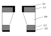
- hole array bases 211 and 212 is formed on the top surface and bottom surface of the silicon substrate 200 , respectively, i.e., a top hole array base 211 is formed on the top surface of the silicon substrate 200 and a bottom hole array base 212 is formed on the bottom surface of the silicon substrate 200 .
- the top hole array base 211 and the bottom hole array base 212 may be formed on the top surface and the bottom surface of the silicon substrate 200 in a manner of deposition.
- the material of the hole array bases 211 and 212 may be low stress silicon nitride or low stress silicon oxide.
- a photoresist is coated on the top hole array base 211 , and the front hole is formed in the top hole array base 211 by the photolithography and the reactive ion etching to expose the silicon substrate 200 .
- the width of the front hole is in a range from tens of nanometers to several microns.
- the top protection layer 221 is formed on the silicon substrate 200 with the top hole array base 211 to cover the surface of the top hole array base 211 , sidewalls of the front hole and the exposed portion of the silicon substrate 200 .
- the bottom protection layer 222 is formed on the bottom hole array base 212 .
- the thickness of the protection layer 222 ranges from 8 nanometers to 20 nanometers, which is proportional to the thickness of the silicon substrate.
- the material of the protection layers 221 and 222 may be low temperature silicon nitride or low temperature silicon oxide.
- the low temperature silicon nitride or the low temperature silicon oxide has a high stress.
- the low temperature silicon nitride or the low temperature silicon oxide has a slower reaction rate during the alkali corrosion.
- the protection layer can protect the covered hole array base from the damage caused by the alkali corrosion solution.
- a photoresist is coated on the bottom protection layer 222 , and the rear window is formed in the bottom protection layer 222 and the bottom hole array base 212 by the photolithography and the reactive ion etching to expose the silicon substrate 200 .
- the shape of the rear window may be a quadrate slot.
- the width of the rear window may be several millimeters.
- the silicon substrate 200 is etched through by the alkali corrosion to connect the front hole with the rear window, so as to form a solid hole array.
- the alkali corrosion may be performed using an alkali corrosion solution such as KOH or tetramethylammonium hydroxide.
- the width of the front hole ranges from tens of nanometers to several microns, and the width of the rear widow may be several millimeters. It can be seen that the width of the rear widow is much wider than that of the front hole.
- the reaction rate of the material of the protection layers 221 and 222 is much slower than that of the material of the silicon substrate when etching the silicon substrate 200 , the alkali corrosion solution reacts on both sides of the protection layer 221 deposited on the top of the silicon substrate after the silicon substrate 200 is etched through, so as to etch this portion of the protection layer rapidly. In this way, the hole array base around the hole is protected when the solid hole array is formed, so as to implement a better control of the feature of the hole in the hole array.
- the solid hole array of the present disclosure is formed based on the above process, specifically shown in FIG. 6 .
- the solid hole array includes the substrate 200 with a via; the top hole array base 211 formed on the top surface of the substrate 200 and the bottom hole array base 212 formed on the bottom surface of the substrate 200 , in which the front hole is located in the top hole array base 211 at a place corresponding to the via; and the top protection lay 221 formed on the surface and sidewalls of the top hole array base 211 and the bottom protection layer 222 formed on the surface of the bottom hole array base 212 , in which the rear window is located in the bottom hole array base 212 and the bottom protection layer 222 at a place corresponding to the via.
- the material of the top hole array base and the bottom hole array base is low stress silicon nitride or low stress silicon oxide.
- the material of the top protection layer and the bottom protection layer is low temperature silicon nitride or low temperature silicon oxide.
- the thickness of the protection layer may ranges from 8 to 20 nanometers.
- the width of the front hole is smaller than that of the rear window.
Abstract
Description
Claims (6)
Applications Claiming Priority (4)
| Application Number | Priority Date | Filing Date | Title |
|---|---|---|---|
| CN201210226670.6A CN103510088B (en) | 2012-06-29 | 2012-06-29 | Solid-state hole array and preparation method thereof |
| CN201210226670.6 | 2012-06-29 | ||
| CN201210226670 | 2012-06-29 | ||
| PCT/CN2012/079388 WO2014000332A1 (en) | 2012-06-29 | 2012-07-31 | Solid-state aperture array and fabrication method thereof |
Publications (2)
| Publication Number | Publication Date |
|---|---|
| US20140001646A1 US20140001646A1 (en) | 2014-01-02 |
| US9136160B2 true US9136160B2 (en) | 2015-09-15 |
Family
ID=49777269
Family Applications (1)
| Application Number | Title | Priority Date | Filing Date |
|---|---|---|---|
| US13/697,372 Active US9136160B2 (en) | 2012-06-29 | 2012-07-31 | Solid hole array and method for forming the same |
Country Status (1)
| Country | Link |
|---|---|
| US (1) | US9136160B2 (en) |
Citations (35)
| Publication number | Priority date | Publication date | Assignee | Title |
|---|---|---|---|---|
| US5393351A (en) * | 1993-01-13 | 1995-02-28 | The United States Of America As Represented By The Secretary Of Commerce | Multilayer film multijunction thermal converters |
| EP0841167A2 (en) | 1996-11-11 | 1998-05-13 | Canon Kabushiki Kaisha | Method of producing a through-hole, silicon substrate having a through-hole, device using such a substrate, method of producing an ink-jet print head, and ink-jet print head |
| US6123861A (en) * | 1996-07-02 | 2000-09-26 | Massachusetts Institute Of Technology | Fabrication of microchip drug delivery devices |
| US20010019029A1 (en) * | 1997-11-07 | 2001-09-06 | California Institute Of Technology | Micromachined membrane particle filter using parylene reinforcement |
| US20030080359A1 (en) * | 2001-10-30 | 2003-05-01 | Canon Kabushiki Kaisha | Structure with through hole, production method thereof, and liquid discharge head |
| US20030137021A1 (en) * | 2002-01-18 | 2003-07-24 | Man Wong | Integrated electronic microphone and a method of manufacturing |
| US20040166140A1 (en) * | 1996-07-02 | 2004-08-26 | Santini John T. | Implantable device for controlled release of drug |
| WO2004077503A2 (en) | 2003-02-03 | 2004-09-10 | President And Fellows Of Harvard College | Controlled fabrication of gaps in electrically conducting structures |
| US6857501B1 (en) * | 1999-09-21 | 2005-02-22 | The United States Of America As Represented By The Secretary Of The Navy | Method of forming parylene-diaphragm piezoelectric acoustic transducers |
| US20050167805A1 (en) * | 2004-02-03 | 2005-08-04 | Nec Electronics Corporation | Semiconductor device and manufacturing method thereof |
| US20060171888A1 (en) * | 2000-03-02 | 2006-08-03 | Microchips, Inc. | Medical Device and Method for Diagnostic Sensing |
| WO2008031255A1 (en) * | 2006-08-18 | 2008-03-20 | He Jian Technology(Suzhou)Co., Ltd | Method of self-aligned silicon nitride overlying for the borderless contact hole of copper technology |
| US7352932B1 (en) * | 2006-09-29 | 2008-04-01 | National Central University | Guided-mode resonance filter and fabrication method of same |
| US20080122431A1 (en) * | 2004-06-07 | 2008-05-29 | General Electric Company | Micro-electromechanical system (mems) based current & magnetic field sensor having improved sensitivities |
| US20080165226A1 (en) * | 1997-07-15 | 2008-07-10 | Silverbrook Research Pty Ltd | Nozzle assembly having a sprung electromagnetically operated plunger |
| US20090097712A1 (en) * | 2007-08-06 | 2009-04-16 | Harris Scott C | Intelligent display screen which interactively selects content to be displayed based on surroundings |
| US20090239377A1 (en) * | 2004-03-04 | 2009-09-24 | Nec Electronics Corporation | Semiconductor device and method for manufacturing the same |
| US20100006959A1 (en) * | 2006-06-14 | 2010-01-14 | Magnachip Semiconductor Ltd. | Package of mems device and method for fabricating the same |
| US20100005877A1 (en) * | 2008-07-10 | 2010-01-14 | Denso Corporation | Semiconductor sensor having heater on insulation film and manufacturing method of the same |
| CN101665231A (en) | 2009-09-18 | 2010-03-10 | 上海芯敏微系统技术有限公司 | Structure of thin film device manufactured by means of double-faced opposite-penetrated corrosion based on (100) silicon chip and method thereof |
| US20100327847A1 (en) * | 2007-09-12 | 2010-12-30 | President And Fellows Of Harvard College | High-Resolution Molecular Sensor |
| US20110053284A1 (en) | 2007-05-08 | 2011-03-03 | The Trustees Of Boston University | Chemical functionalization of solid-state nanopores and nanopore arrays and applications thereof |
| US20110175228A1 (en) * | 2004-11-22 | 2011-07-21 | Intermolecular, Inc. | Molecular self-assembly in substrate processing |
| US20110305258A1 (en) * | 2008-09-09 | 2011-12-15 | Mohamed Boutchich | Planar Thermopile Infrared Microsensor |
| US20110316169A1 (en) * | 2010-06-24 | 2011-12-29 | Shinko Electric Industries Co., Ltd. | Wiring substrate and method for manufacturing the wiring substrate |
| US20120007257A1 (en) * | 2009-04-03 | 2012-01-12 | Panasonic Corporation | Semiconductor device and manufacturing method thereof |
| CN102328899A (en) | 2011-08-05 | 2012-01-25 | 上海先进半导体制造股份有限公司 | Method for manufacturing cavities of different depths |
| US20120021204A1 (en) | 2010-07-26 | 2012-01-26 | International Business Machines Corporation | Structure and method to form nanopore |
| US20120040512A1 (en) | 2010-08-11 | 2012-02-16 | Globalfoundries | Method to form nanopore array |
| US20120169320A1 (en) * | 2010-12-30 | 2012-07-05 | Molecular Devices, Llc | Planar patch clamp devices and methods for fabrication and use |
| US20120182548A1 (en) * | 2009-07-23 | 2012-07-19 | Insight Nanofluidics Inc | Nanofluidic cell |
| US8409901B2 (en) * | 2008-03-11 | 2013-04-02 | The Royal Institution For The Advancement Of Learning/Mcgill University | Low temperature wafer level processing for MEMS devices |
| US20130092541A1 (en) * | 2010-02-19 | 2013-04-18 | The Trustees Of The University Of Pennsylvania | High-Resolution Analysis Devices and Related Methods |
| US20130264219A1 (en) * | 2012-04-04 | 2013-10-10 | International Business Machines Corporation | Functionally switchable self-assembled coating compound for controlling translocation of molecule through nanopores |
| US20140106563A1 (en) * | 2012-02-09 | 2014-04-17 | Taiwan Semiconductor Manufacturing Company, Ltd. | Stress Reduction Apparatus |
-
2012
- 2012-07-31 US US13/697,372 patent/US9136160B2/en active Active
Patent Citations (38)
| Publication number | Priority date | Publication date | Assignee | Title |
|---|---|---|---|---|
| US5393351A (en) * | 1993-01-13 | 1995-02-28 | The United States Of America As Represented By The Secretary Of Commerce | Multilayer film multijunction thermal converters |
| US6123861A (en) * | 1996-07-02 | 2000-09-26 | Massachusetts Institute Of Technology | Fabrication of microchip drug delivery devices |
| US20040166140A1 (en) * | 1996-07-02 | 2004-08-26 | Santini John T. | Implantable device for controlled release of drug |
| US20080047926A1 (en) * | 1996-07-02 | 2008-02-28 | Massachusetts Institute Of Technology | Method for Making Microchip Reservoir Device |
| EP0841167A2 (en) | 1996-11-11 | 1998-05-13 | Canon Kabushiki Kaisha | Method of producing a through-hole, silicon substrate having a through-hole, device using such a substrate, method of producing an ink-jet print head, and ink-jet print head |
| US20080165226A1 (en) * | 1997-07-15 | 2008-07-10 | Silverbrook Research Pty Ltd | Nozzle assembly having a sprung electromagnetically operated plunger |
| US20010019029A1 (en) * | 1997-11-07 | 2001-09-06 | California Institute Of Technology | Micromachined membrane particle filter using parylene reinforcement |
| US6857501B1 (en) * | 1999-09-21 | 2005-02-22 | The United States Of America As Represented By The Secretary Of The Navy | Method of forming parylene-diaphragm piezoelectric acoustic transducers |
| US20060171888A1 (en) * | 2000-03-02 | 2006-08-03 | Microchips, Inc. | Medical Device and Method for Diagnostic Sensing |
| US20030080359A1 (en) * | 2001-10-30 | 2003-05-01 | Canon Kabushiki Kaisha | Structure with through hole, production method thereof, and liquid discharge head |
| US20030137021A1 (en) * | 2002-01-18 | 2003-07-24 | Man Wong | Integrated electronic microphone and a method of manufacturing |
| WO2004077503A2 (en) | 2003-02-03 | 2004-09-10 | President And Fellows Of Harvard College | Controlled fabrication of gaps in electrically conducting structures |
| US20050167805A1 (en) * | 2004-02-03 | 2005-08-04 | Nec Electronics Corporation | Semiconductor device and manufacturing method thereof |
| US20090239377A1 (en) * | 2004-03-04 | 2009-09-24 | Nec Electronics Corporation | Semiconductor device and method for manufacturing the same |
| US20080122431A1 (en) * | 2004-06-07 | 2008-05-29 | General Electric Company | Micro-electromechanical system (mems) based current & magnetic field sensor having improved sensitivities |
| US20110175228A1 (en) * | 2004-11-22 | 2011-07-21 | Intermolecular, Inc. | Molecular self-assembly in substrate processing |
| US20100006959A1 (en) * | 2006-06-14 | 2010-01-14 | Magnachip Semiconductor Ltd. | Package of mems device and method for fabricating the same |
| WO2008031255A1 (en) * | 2006-08-18 | 2008-03-20 | He Jian Technology(Suzhou)Co., Ltd | Method of self-aligned silicon nitride overlying for the borderless contact hole of copper technology |
| US7352932B1 (en) * | 2006-09-29 | 2008-04-01 | National Central University | Guided-mode resonance filter and fabrication method of same |
| US20110053284A1 (en) | 2007-05-08 | 2011-03-03 | The Trustees Of Boston University | Chemical functionalization of solid-state nanopores and nanopore arrays and applications thereof |
| US20090097712A1 (en) * | 2007-08-06 | 2009-04-16 | Harris Scott C | Intelligent display screen which interactively selects content to be displayed based on surroundings |
| US20100327847A1 (en) * | 2007-09-12 | 2010-12-30 | President And Fellows Of Harvard College | High-Resolution Molecular Sensor |
| US8409901B2 (en) * | 2008-03-11 | 2013-04-02 | The Royal Institution For The Advancement Of Learning/Mcgill University | Low temperature wafer level processing for MEMS devices |
| US20100005877A1 (en) * | 2008-07-10 | 2010-01-14 | Denso Corporation | Semiconductor sensor having heater on insulation film and manufacturing method of the same |
| US20110305258A1 (en) * | 2008-09-09 | 2011-12-15 | Mohamed Boutchich | Planar Thermopile Infrared Microsensor |
| US20120007257A1 (en) * | 2009-04-03 | 2012-01-12 | Panasonic Corporation | Semiconductor device and manufacturing method thereof |
| US20120182548A1 (en) * | 2009-07-23 | 2012-07-19 | Insight Nanofluidics Inc | Nanofluidic cell |
| CN101665231A (en) | 2009-09-18 | 2010-03-10 | 上海芯敏微系统技术有限公司 | Structure of thin film device manufactured by means of double-faced opposite-penetrated corrosion based on (100) silicon chip and method thereof |
| US20130092541A1 (en) * | 2010-02-19 | 2013-04-18 | The Trustees Of The University Of Pennsylvania | High-Resolution Analysis Devices and Related Methods |
| US20110316169A1 (en) * | 2010-06-24 | 2011-12-29 | Shinko Electric Industries Co., Ltd. | Wiring substrate and method for manufacturing the wiring substrate |
| US20120021204A1 (en) | 2010-07-26 | 2012-01-26 | International Business Machines Corporation | Structure and method to form nanopore |
| US20120040512A1 (en) | 2010-08-11 | 2012-02-16 | Globalfoundries | Method to form nanopore array |
| US8138068B2 (en) | 2010-08-11 | 2012-03-20 | International Business Machines Corporation | Method to form nanopore array |
| US20120169320A1 (en) * | 2010-12-30 | 2012-07-05 | Molecular Devices, Llc | Planar patch clamp devices and methods for fabrication and use |
| CN102328899A (en) | 2011-08-05 | 2012-01-25 | 上海先进半导体制造股份有限公司 | Method for manufacturing cavities of different depths |
| US20140106563A1 (en) * | 2012-02-09 | 2014-04-17 | Taiwan Semiconductor Manufacturing Company, Ltd. | Stress Reduction Apparatus |
| US20130264219A1 (en) * | 2012-04-04 | 2013-10-10 | International Business Machines Corporation | Functionally switchable self-assembled coating compound for controlling translocation of molecule through nanopores |
| US20130263946A1 (en) * | 2012-04-04 | 2013-10-10 | International Business Machines Corporation | Functionally switchable self-assembled coating compound for controlling translocation of molecule through nanopores |
Non-Patent Citations (2)
| Title |
|---|
| International Search Report (Jul. 31, 2012) (in Chinese). |
| Written Opinion (Jul. 31, 2012) (in Chinese). |
Also Published As
| Publication number | Publication date |
|---|---|
| US20140001646A1 (en) | 2014-01-02 |
Similar Documents
| Publication | Publication Date | Title |
|---|---|---|
| CN103958397B (en) | For the application of the method and this method that manufacture and be aligned nano wire | |
| CN103794490B (en) | Method for forming self-aligned double pattern | |
| US9437441B2 (en) | Methods for etching substrate and semiconductor devices | |
| US9490163B2 (en) | Tapered sidewall conductive lines and formation thereof | |
| CN103738914B (en) | The manufacture method of MEMS | |
| KR20150097572A (en) | Fabrication of three-dimensional high surface area electrodes | |
| CN106044759B (en) | A kind of regulation graphene band gap method | |
| CN102354669B (en) | Production method of silicon nano-wire device | |
| CN105810615A (en) | Method and system for monitoring in-situ etching of etching sample by employing crystal oscillator | |
| US20060148129A1 (en) | Silicon direct bonding method | |
| CN105489480B (en) | The method that grid is formed using Dual graphing technology | |
| CN104051274B (en) | Method for processing a carrier | |
| US20170194444A1 (en) | Methods and structures for a split gate memory cell structure | |
| US20210165314A1 (en) | Method of creating a nano-sized recess | |
| CN106952949B (en) | Graphene field effect transistor and forming method thereof | |
| US9136160B2 (en) | Solid hole array and method for forming the same | |
| Asano et al. | A novel wafer dicing method using metal-assisted chemical etching | |
| US10586856B2 (en) | Nanosheet FET device with epitaxial nucleation | |
| CN103839795B (en) | The manufacture method of floating boom and the manufacture method of floating transistor | |
| US20090156009A1 (en) | Method for manufacturing semiconductor device | |
| US8642484B2 (en) | Method for manufacturing semiconductor device | |
| CN105502281A (en) | Metal patterning method | |
| CN110174453B (en) | Microelectrode structure, manufacturing method thereof and electronic equipment comprising microelectrode structure | |
| US20130200437A1 (en) | Method of forming nanogap pattern, biosensor having the nanogap pattern, and method of manufacturing the biosensor | |
| US9012274B2 (en) | Method of manufacturing a semiconductor fin using sacrificial layer |
Legal Events
| Date | Code | Title | Description |
|---|---|---|---|
| AS | Assignment |
Owner name: INSTITUTE OF MICROELECTRONICS, CHINESE ACADEMY OF Free format text: ASSIGNMENT OF ASSIGNORS INTEREST;ASSIGNORS:DONG, LIJUN;ZHAO, CHAO;REEL/FRAME:029276/0974 Effective date: 20121105 |
|
| STCF | Information on status: patent grant |
Free format text: PATENTED CASE |
|
| MAFP | Maintenance fee payment |
Free format text: PAYMENT OF MAINTENANCE FEE, 4TH YR, SMALL ENTITY (ORIGINAL EVENT CODE: M2551); ENTITY STATUS OF PATENT OWNER: SMALL ENTITY Year of fee payment: 4 |
|
| MAFP | Maintenance fee payment |
Free format text: PAYMENT OF MAINTENANCE FEE, 8TH YR, SMALL ENTITY (ORIGINAL EVENT CODE: M2552); ENTITY STATUS OF PATENT OWNER: SMALL ENTITY Year of fee payment: 8 |