EP3485508B1 - Vorrichtung zur handhabung einer halbleiterscheibe in einem epitaxie-reaktor und verfahren zur herstellung einer halbleiterscheibe mit epitaktischer schicht - Google Patents
Vorrichtung zur handhabung einer halbleiterscheibe in einem epitaxie-reaktor und verfahren zur herstellung einer halbleiterscheibe mit epitaktischer schicht Download PDFInfo
- Publication number
- EP3485508B1 EP3485508B1 EP17739514.2A EP17739514A EP3485508B1 EP 3485508 B1 EP3485508 B1 EP 3485508B1 EP 17739514 A EP17739514 A EP 17739514A EP 3485508 B1 EP3485508 B1 EP 3485508B1
- Authority
- EP
- European Patent Office
- Prior art keywords
- susceptor
- semiconductor wafer
- pins
- susceptor support
- wafer
- Prior art date
- Legal status (The legal status is an assumption and is not a legal conclusion. Google has not performed a legal analysis and makes no representation as to the accuracy of the status listed.)
- Active
Links
Images

Classifications
-
- H—ELECTRICITY
- H10—SEMICONDUCTOR DEVICES; ELECTRIC SOLID-STATE DEVICES NOT OTHERWISE PROVIDED FOR
- H10P—GENERIC PROCESSES OR APPARATUS FOR THE MANUFACTURE OR TREATMENT OF DEVICES COVERED BY CLASS H10
- H10P72/00—Handling or holding of wafers, substrates or devices during manufacture or treatment thereof
- H10P72/70—Handling or holding of wafers, substrates or devices during manufacture or treatment thereof for supporting or gripping
- H10P72/76—Handling or holding of wafers, substrates or devices during manufacture or treatment thereof for supporting or gripping using mechanical means, e.g. clamps or pinches
- H10P72/7604—Handling or holding of wafers, substrates or devices during manufacture or treatment thereof for supporting or gripping using mechanical means, e.g. clamps or pinches the wafers being placed on a susceptor, stage or support
- H10P72/7612—Handling or holding of wafers, substrates or devices during manufacture or treatment thereof for supporting or gripping using mechanical means, e.g. clamps or pinches the wafers being placed on a susceptor, stage or support characterised by lifting arrangements, e.g. lift pins
-
- C—CHEMISTRY; METALLURGY
- C30—CRYSTAL GROWTH
- C30B—SINGLE-CRYSTAL GROWTH; UNIDIRECTIONAL SOLIDIFICATION OF EUTECTIC MATERIAL OR UNIDIRECTIONAL DEMIXING OF EUTECTOID MATERIAL; REFINING BY ZONE-MELTING OF MATERIAL; PRODUCTION OF A HOMOGENEOUS POLYCRYSTALLINE MATERIAL WITH DEFINED STRUCTURE; SINGLE CRYSTALS OR HOMOGENEOUS POLYCRYSTALLINE MATERIAL WITH DEFINED STRUCTURE; AFTER-TREATMENT OF SINGLE CRYSTALS OR A HOMOGENEOUS POLYCRYSTALLINE MATERIAL WITH DEFINED STRUCTURE; APPARATUS THEREFOR
- C30B25/00—Single-crystal growth by chemical reaction of reactive gases, e.g. chemical vapour-deposition growth
- C30B25/02—Epitaxial-layer growth
- C30B25/12—Substrate holders or susceptors
-
- C—CHEMISTRY; METALLURGY
- C30—CRYSTAL GROWTH
- C30B—SINGLE-CRYSTAL GROWTH; UNIDIRECTIONAL SOLIDIFICATION OF EUTECTIC MATERIAL OR UNIDIRECTIONAL DEMIXING OF EUTECTOID MATERIAL; REFINING BY ZONE-MELTING OF MATERIAL; PRODUCTION OF A HOMOGENEOUS POLYCRYSTALLINE MATERIAL WITH DEFINED STRUCTURE; SINGLE CRYSTALS OR HOMOGENEOUS POLYCRYSTALLINE MATERIAL WITH DEFINED STRUCTURE; AFTER-TREATMENT OF SINGLE CRYSTALS OR A HOMOGENEOUS POLYCRYSTALLINE MATERIAL WITH DEFINED STRUCTURE; APPARATUS THEREFOR
- C30B29/00—Single crystals or homogeneous polycrystalline material with defined structure characterised by the material or by their shape
- C30B29/02—Elements
- C30B29/06—Silicon
-
- H—ELECTRICITY
- H10—SEMICONDUCTOR DEVICES; ELECTRIC SOLID-STATE DEVICES NOT OTHERWISE PROVIDED FOR
- H10P—GENERIC PROCESSES OR APPARATUS FOR THE MANUFACTURE OR TREATMENT OF DEVICES COVERED BY CLASS H10
- H10P72/00—Handling or holding of wafers, substrates or devices during manufacture or treatment thereof
- H10P72/30—Handling or holding of wafers, substrates or devices during manufacture or treatment thereof for conveying, e.g. between different workstations
- H10P72/33—Handling or holding of wafers, substrates or devices during manufacture or treatment thereof for conveying, e.g. between different workstations into and out of processing chamber
- H10P72/3302—Mechanical parts of transfer devices
-
- H—ELECTRICITY
- H10—SEMICONDUCTOR DEVICES; ELECTRIC SOLID-STATE DEVICES NOT OTHERWISE PROVIDED FOR
- H10P—GENERIC PROCESSES OR APPARATUS FOR THE MANUFACTURE OR TREATMENT OF DEVICES COVERED BY CLASS H10
- H10P72/00—Handling or holding of wafers, substrates or devices during manufacture or treatment thereof
- H10P72/70—Handling or holding of wafers, substrates or devices during manufacture or treatment thereof for supporting or gripping
- H10P72/76—Handling or holding of wafers, substrates or devices during manufacture or treatment thereof for supporting or gripping using mechanical means, e.g. clamps or pinches
- H10P72/7604—Handling or holding of wafers, substrates or devices during manufacture or treatment thereof for supporting or gripping using mechanical means, e.g. clamps or pinches the wafers being placed on a susceptor, stage or support
- H10P72/7626—Handling or holding of wafers, substrates or devices during manufacture or treatment thereof for supporting or gripping using mechanical means, e.g. clamps or pinches the wafers being placed on a susceptor, stage or support characterised by the construction of the shaft
-
- H—ELECTRICITY
- H10—SEMICONDUCTOR DEVICES; ELECTRIC SOLID-STATE DEVICES NOT OTHERWISE PROVIDED FOR
- H10P—GENERIC PROCESSES OR APPARATUS FOR THE MANUFACTURE OR TREATMENT OF DEVICES COVERED BY CLASS H10
- H10P72/00—Handling or holding of wafers, substrates or devices during manufacture or treatment thereof
- H10P72/70—Handling or holding of wafers, substrates or devices during manufacture or treatment thereof for supporting or gripping
- H10P72/76—Handling or holding of wafers, substrates or devices during manufacture or treatment thereof for supporting or gripping using mechanical means, e.g. clamps or pinches
- H10P72/7604—Handling or holding of wafers, substrates or devices during manufacture or treatment thereof for supporting or gripping using mechanical means, e.g. clamps or pinches the wafers being placed on a susceptor, stage or support
- H10P72/7624—Handling or holding of wafers, substrates or devices during manufacture or treatment thereof for supporting or gripping using mechanical means, e.g. clamps or pinches the wafers being placed on a susceptor, stage or support characterised by the mechanical construction of the susceptor, stage or support
Definitions
- the invention relates to a device for handling a semiconductor wafer in an epitaxial reactor.
- the invention also relates to a method for producing a semiconductor wafer with an epitaxial layer, in which the device is used.
- An epitaxial layer is usually deposited on a semiconductor wafer by means of CVD (chemical vapor deposition) in an epitaxial reactor, often in a single wafer reactor.
- CVD chemical vapor deposition
- US 2014/0 251 208 A1 and US 2010/0 086 784 A1 contain descriptions of details of such epitaxial reactors.
- An elementary part of the handling of a semiconductor wafer comprises, before the deposition of the epitaxial layer, the laying down of the semiconductor wafer on a susceptor and, after the deposition of the epitaxial layer, the lifting of the semiconductor wafer with the epitaxial layer from the susceptor.
- the device used for this includes a disk lifting shaft and disk lifting pins, a susceptor support shaft, susceptor support arms and susceptor support pins.
- the disk lift shaft has cantilevers at the top that extend sideways upward and terminate under the disk lift pins.
- the wafer lifting pins and a semiconductor wafer or semiconductor wafer with an epitaxial layer, which may have been deposited on the pins are also lowered and also raised.
- the disc lifting pins are pushed through holes that are located in the susceptor support arms of the susceptor support shaft and through holes in the susceptor.
- the disadvantage of the device described is that its use is susceptible to generating particles, and the particles contaminate the rear side of the semiconductor wafer facing the susceptor.
- the particles are created as abrasion due to friction between the washer lift pins and the inner surfaces of the holes in the susceptor support arms and the through holes in the susceptor.
- the friction is also due in particular to the fact that the device must remain functional over a wide temperature range and thermal expansion at high temperatures must be taken into account.
- the washer lift pins are also prone to tilting from the vertical position. In such a situation, additional particles are created.
- the object of the invention arose from this problem.
- a device for handling a semiconductor wafer in an epitaxial reactor comprising a susceptor; elongated holes leading through the susceptor; a disk lift shaft; Washer lifting pins passed through the elongated holes; a susceptor support shaft; Susceptor support arms; Susceptor support pins; Guide sleeves anchored in the susceptor support arms; and guide elements which protrude from the guide sleeves and have bores at upper ends into which the disk lifting pins are inserted and which can be raised and lowered by means of the disk lifting shaft together with the disk lifting pins.
- the object is further achieved by a method for producing a semiconductor wafer with an epitaxial layer, comprising the provision of a device according to the invention in an epitaxial reactor; depositing a semiconductor wafer on the wafer lift pins; placing the wafer on the susceptor by lowering the wafer lift pins; depositing the epitaxial layer on the semiconductor wafer; lifting the resulting epitaxial layer semiconductor wafer from the susceptor by lifting the wafer lift pins; and removing the semiconductor wafer with the epitaxial layer from the epitaxial reactor.
- the use of the proposed device suppresses the formation of particles in the course of the lowering of the semiconductor wafer from the susceptor and the lifting of the semiconductor wafer with an epitaxial layer from the susceptor and, in particular, avoids that the back of the semiconductor wafer or the back of the semiconductor wafer with epitaxial layer is contaminated by particles.
- properties such as concentricity, radial runout and vertical runout of the device are minimized because of its design.
- the device is designed in such a way that the disk lifting pins are moved linearly guided through elongated holes in the susceptor. Particle formation due to friction is suppressed regardless of the prevailing operating temperature.
- At least three susceptor support arms are preferably formed from a one-piece element which is attached to the upper end of the susceptor support shaft.
- a star-shaped element made of quartz, which is screwed to the susceptor support shaft, is particularly preferred.
- the star-shaped element can, however, also be in several parts and comprise struts made of quartz which are mounted, for example screwed, on the susceptor support shaft.
- Guide sleeves are anchored, preferably screwed, in the susceptor support arms, so that they can easily be exchanged if necessary.
- the guide sleeves preferably have ground inner surfaces and are preferably made of quartz.
- the mean roughness Ra of the inner surfaces is preferably not more than 0.4 ⁇ m.
- the guide sleeves and guide elements in the guide sleeves, which protrude from the guide sleeves at both ends, each form linear sliding bearings that ensure the linearly guided movement of the disc lifting pins.
- the rod-shaped guide elements consist of the same material as the guide sleeves and have outer surfaces whose mean roughness Ra is preferably likewise not more than 0.4 ⁇ m.
- the guide sleeves and the guide elements there is therefore hardly any friction between the guide sleeves and the guide elements, so that hardly any particles are produced, and if at all, only at a location with a sufficient distance from the susceptor and a semiconductor wafer lying on it, so that contamination of the rear side of the semiconductor wafer by particles is excluded.
- the arrangement of guide sleeves and guide elements and elongated holes prevents particles from being generated in the immediate vicinity of the semiconductor wafer when the wafer lifting pins are raised and lowered.
- unintentional tilting of the disc lifting pins from the vertical position is also not possible.
- the disk lifting pins which preferably have upper ends with a T-shaped cross section, are inserted into bores in the guide elements which have the guide elements at the upper ends.
- the disk lifting pins and the bores of the guide elements are preferably dimensioned such that the disk lifting pins are centered when they are inserted into the bores of the guide elements at room temperature.
- the disc lifting pins are made from a different material with a different thermal expansion than the guide elements, preferably from silicon carbide.
- the manufacturing tolerances of the disk lifting pins and the guide elements are also dimensioned such that the disk lifting pins are clampingly connected to the guide elements at temperatures that are set when the epitaxial layer is deposited.
- the clamping connection is preferably formed at temperatures of more than 900 ° C. Because of the clamping connection, the disc lifting pins have no radial play, which helps to suppress the formation of particles.
- This configuration also ensures that the disk lifting pins and the elongated holes in the susceptor always remain aligned at least in a temperature range that extends from room temperature to the deposition temperature. In addition, this ensures that the T-shaped ends of the disk lifting pins can be placed on the susceptor synchronously and lifted off the susceptor.
- the disk lifting shaft and the guide elements which rest on outer ends of arms of the disk lifting shaft, are raised or lowered.
- upright elements are attached to the outer ends of the susceptor support arms in a height-adjustable manner, preferably screwed on.
- the upper ends of the post elements have axial bores in which susceptor support pins are inserted, the heads of which are preferably rounded in a spherical shape.
- On the back of the susceptor there are blind holes with an elongated base area for receiving the spherically rounded heads of the susceptor support pins.
- the length and width of the blind holes increase in the direction of the opening of the blind holes.
- the blind holes for the susceptor support pins preferably form a support with a prism-shaped contour. This embodiment allows a low-friction radial movement of the susceptor, in particular a self-centering movement triggered by thermal expansion of the susceptor material.
- the susceptor preferably has a plate-shaped cross section and comprises an annular storage surface designed as a ledge and a susceptor base.
- the semiconductor wafer lies in the edge area with the rear side on the annular storage surface and is at a small distance from the susceptor base.
- the susceptor can be designed in one piece or can be formed by a ring and a flat susceptor base, the ring lying on the flat susceptor base.
- the elongated holes and the blind holes are arranged in the susceptor base.
- the device according to Fig.1 comprises a susceptor support shaft 4 and a disk lifting shaft 2.
- Susceptor support arms 5 at equal distances from one another are combined to form a one-piece, star-shaped element which is screwed to the upper end of the susceptor support shaft 4.
- the disc lifting shaft 2 comprises cantilevers projecting radially upward, at the ends of which platforms are provided for supporting guide elements 8.
- the guide elements 8 are pushed through guide sleeves 7 that are anchored in the susceptor support arms 5.
- the upper ends of the guide elements 8 have bores into which disk lifting pins 3 are inserted.
- the disk lifting pins 3 extend through elongated holes 11 in the susceptor 1.
- the susceptor 1 has blind holes 12 with an elongated base on the back and rests there on spherically rounded heads 10 of susceptor support pins 6.
- the susceptor support pins 6 are in axial bores upper ends of upright elements 9.
- the upright elements 9 are fastened on the susceptor support arms 5 at their outer ends so as to be adjustable in height.
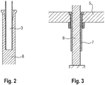
- FIG. 2 shows an enlarged illustration of the upper end of the guide element 8 with the bore provided there and the lower end of the disc lifting pin 3 inserted into the bore. This area is shown in FIG Fig.1 marked with a circle and the letter A.
- Fig. 3 shows an enlarged view of the guide sleeve 7, which is anchored in the susceptor support arm 5, and part of the guide element 8, which is pushed through the guide sleeve 7 and stands at the lower end on a platform of the boom of the disc lifting shaft 2.
- This area is in Fig.1 marked with a circle and the letter B.
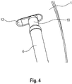
- Fig. 4 shows an enlarged illustration of the upper end of the susceptor support pin 6 and the spherically rounded head 10 of the susceptor support pin, which protrudes into the blind hole 12 on the rear side of the susceptor 1.
- This area is in Fig.1 marked with a circle and the letter C.
Landscapes
- Chemical & Material Sciences (AREA)
- Engineering & Computer Science (AREA)
- Crystallography & Structural Chemistry (AREA)
- Materials Engineering (AREA)
- Metallurgy (AREA)
- Organic Chemistry (AREA)
- Chemical Kinetics & Catalysis (AREA)
- General Chemical & Material Sciences (AREA)
- Container, Conveyance, Adherence, Positioning, Of Wafer (AREA)
- Chemical Vapour Deposition (AREA)
- Crystals, And After-Treatments Of Crystals (AREA)
- Robotics (AREA)
Description
- Gegenstand der Erfindung ist eine Vorrichtung zur Handhabung einer Halbleiterscheibe in einem Epitaxie-Reaktor. Darüber hinaus betrifft die Erfindung ein Verfahren zur Herstellung einer Halbleiterscheibe mit epitaktischer Schicht, bei dem die Vorrichtung eingesetzt wird.
- Das Abscheiden einer epitaktischen Schicht auf einer Halbleiterscheibe geschieht üblicherweise mittels CVD (chemical vapor deposition) in einem Epitaxie-Reaktor, häufig in einem Einzelscheiben-Reaktor.
-
US 2014/0 251 208 A1 undUS 2010/0 086 784 A1 enthalten Beschreibungen von Einzelheiten solcher Epitaxie-Reaktoren. Ein elementarer Teil der Handhabung einer Halbleiterscheibe umfasst vor dem Abscheiden der epitaktischen Schicht das Ablegen der Halbleiterscheibe auf einem Suszeptor und nach dem Abscheiden der epitaktischen Schicht das Anheben der Halbleiterscheibe mit epitaktischer Schicht vom Suszeptor. Die dafür eingesetzte Vorrichtung umfasst neben dem Suszeptor eine Scheiben-Hebewelle und Scheiben-Hebestifte, eine Suszeptor-Tragwelle, Suszeptor-Tragarme und Suszeptor-Stützstifte. - Die Dokumente
US2003/0015141-A1 ,US2004/0241992-A1 ,US6435798-B1 undUS2010/0101491-A1 offenbaren ebenfalls Vorrichtungen mit Hebestiften zur Handhabung von Halbleiterscheiben. - Die Scheiben-Hebewelle hat am oberen Ende Ausleger, die sich seitwärts nach oben erstrecken und unter den Scheiben-Hebestiften enden. Beim Absenken und Anheben der Scheiben-Hebewelle werden die Scheiben-Hebestifte und eine gegebenenfalls auf den Stiften abgelegte Halbleiterscheibe beziehungsweise Halbleiterscheibe mit epitaktischer Schicht mit abgesenkt und mit angehoben. Die Scheiben-Hebestifte werden dabei durch Löcher geschoben, die sich in den Suszeptor-Tragarmen der Suszeptor-Tragwelle befinden, sowie durch Durchgangsbohrungen im Suszeptor. Nachteilig an der beschriebenen Vorrichtung ist, dass ihre Verwendung anfällig ist Partikel zu erzeugen, und die Partikel die Rückseite der Halbleiterscheibe, die dem Suszeptor zugewandt ist, kontaminieren. Die Partikel entstehen als Abrieb in Folge von Reibung zwischen den Scheiben-Hebestiften und den Innenflächen der Löcher in den Suszeptor-Tragarmen und der Durchgangsbohrungen im Suszeptor. Die Reibung ist besonders auch dem Umstand geschuldet, dass die Vorrichtung in einem breiten Temperaturbereich funktionstüchtig bleiben muss und Wärmeausdehnung bei hoher Temperatur zu berücksichtigen ist. Die Scheiben-Hebestifte sind auch dafür anfällig, aus der vertikalen Lage zu verkippen. In einer solchen Situation entstehen zusätzlich Partikel.
- Aus dieser Problematik ergab sich die Aufgabenstellung der Erfindung.
- Die Aufgabe der Erfindung wird gelöst durch eine Vorrichtung zur Handhabung einer Halbleiterscheibe in einem Epitaxie-Reaktor, umfassend
einen Suszeptor;
durch den Suszeptor führende Langlöcher;
eine Scheiben-Hebewelle;
Scheiben-Hebestifte, die durch die Langlöcher geführt sind;
eine Suszeptor-Tragwelle;
Suszeptor-Tragarme;
Suszeptor-Stützstifte;
Führungshülsen, die in den Suszeptor-Tragarmen verankert sind; und Führungselemente, die aus den Führungshülsen ragen und an oberen Enden Bohrungen aufweisen, in denen die Scheiben-Hebestifte stecken, und die mittels der Scheiben-Hebewelle zusammen mit den Scheiben-Hebestiften heb- und absenkbar sind. - Die Aufgabe wird des Weiteren gelöst durch ein Verfahren zur Herstellung einer Halbleiterscheibe mit epitaktischer Schicht, umfassend
das Bereitstellen einer erfindungsgemäßen Vorrichtung in einem Epitaxie-Reaktor; das Ablegen einer Halbleiterscheibe auf den Scheiben-Hebestiften;
das Ablegen der Halbleiterscheibe auf dem Suszeptor durch Absenken der Scheiben-Hebestifte;
das Abscheiden der epitaktischen Schicht auf der Halbleiterscheibe;
das Anheben der entstandenen Halbleiterscheibe mit epitaktischer Schicht vom Suszeptor durch Anheben der Scheiben-Hebestifte; und
das Entfernen der Halbleiterscheibe mit epitaktischer Schicht aus dem Epitaxie-Reaktor. - Die Verwendung der vorgeschlagenen Vorrichtung unterdrückt das Entstehen von Partikeln im Zuge des Absenkens der Halbleiterscheibe vom Suszeptor und des Anhebens der Halbleiterscheibe mit epitaktischer Schicht vom Suszeptor und vermeidet insbesondere, dass die Rückseite der Halbleiterscheibe oder die Rückseite der Halbleiterscheibe mit epitaktischer Schicht durch Partikel kontaminiert wird. Darüber hinaus werden Eigenschaften wie Rundlauf, radialer Schlag und Höhenschlag der Vorrichtung wegen deren Ausgestaltung minimiert.
- Die Vorrichtung ist insbesondere so gestaltet, dass die Scheiben-Hebestifte linear geführt durch Langlöcher im Suszeptor bewegt werden. Partikelbildung durch Reibung wird unabhängig von der vorherrschenden Betriebstemperatur unterdrückt.
- Mindestens drei Suszeptor-Tragarme werden vorzugsweise von einem einteiligen Element gebildet, das am oberen Ende der Suszeptor-Tragwelle befestigt ist. Besonders bevorzugt ist ein sternförmiges Element aus Quarz, das an die Suszeptor-Tragwelle geschraubt ist. Das sternförmige Element kann aber auch mehrteilig sein und Streben aus Quarz umfassen, die an die Suszeptor-Tragwelle montiert, beispielsweise geschraubt sind.
- In den Suszeptor-Tragarmen sind Führungshülsen verankert, vorzugsweise geschraubt, so dass sie bei Bedarf einfach ausgetauscht werden können. Die Führungshülsen haben vorzugsweise geschliffene Innenflächen und bestehen vorzugsweise aus Quarz. Die mittlere Rauheit Ra der Innenflächen beträgt vorzugsweise nicht mehr als 0,4 µm. Die Führungshülsen und Führungselemente in den Führungshülsen, die aus den Führungshülsen an beiden Enden herausragen, bilden jeweils Lineargleitlager, die die linear geführte Bewegung der Scheiben-Hebestifte gewährleisten. Die stabförmigen Führungselemente bestehen aus demselben Material wie die Führungshülsen und haben Außenflächen, deren mittlere Rauheit Ra vorzugsweise ebenfalls nicht mehr als 0,4 µm beträgt. Zwischen den Führungshülsen und den Führungselementen findet daher kaum Reibung statt, so dass auch kaum Partikel entstehen, und wenn überhaupt, nur an einem Ort mit ausreichend Abstand zum Suszeptor und einer darauf liegenden Halbleiterscheibe, so dass eine Kontamination der Rückseite der Halbleiterscheibe durch Partikel ausgeschlossen ist. Insbesondere verhindert die Anordnung von Führungshülsen und Führungselementen und Langlöchern, dass beim Anheben und Absenken der Scheiben-Hebestifte Partikel in unmittelbarer Nähe der Halbleiterscheibe erzeugt werden. Darüber hinaus ist auch ein unabsichtliches Verkippen der Scheiben-Hebestifte aus der vertikalen Lage nicht möglich.
- Die Scheiben-Hebestifte, die vorzugsweise obere Enden mit T-förmigem Querschnitt haben, stecken in Bohrungen der Führungselemente, die die Führungselemente an oberen Enden aufweisen. Die Scheiben-Hebestifte und die Bohrungen der Führungselemente sind vorzugsweise so dimensioniert, dass die Scheiben-Hebestifte zentriert werden, wenn sie bei Raumtemperatur in die Bohrungen der Führungselemente gesteckt werden. Gemäß einer bevorzugten Ausgestaltung sind die Scheiben-Hebestifte aus einem anderen Material mit anderer Wärmeausdehnung gefertigt, als die Führungselemente, vorzugsweise aus Siliziumcarbid. In diesem Fall sind die Fertigungstoleranzen der Scheiben-Hebestifte und der Führungselemente darüber hinaus so bemessen, dass bei Temperaturen, die beim Abscheiden der epitaktischen Schicht eingestellt werden, die Scheiben-Hebestifte mit den Führungselementen klemmend verbunden sind. Vorzugsweise entsteht die klemmende Verbindung bei Temperaturen von mehr als 900 °C. Wegen der klemmenden Verbindung haben die Scheiben-Hebestifte kein radiales Spiel, was zur Unterdrückung der Bildung von Partikeln beiträgt.
- Diese Ausgestaltung gewährleistet auch, dass die Scheiben-Hebestifte und die Langlöcher im Suszeptor mindestens in einem Temperaturbereich, der sich von Raumtemperatur bis zur Abscheidetemperatur erstreckt, stets fluchtend ausgerichtet bleiben. Darüber hinaus ist so sichergestellt, dass die T-förmigen Enden der Scheiben-Hebestifte synchron auf dem Suszeptor abgelegt und vom Suszeptor abgehoben werden können.
- Zur Bewegung der Scheiben-Hebestifte werden die Scheiben-Hebewelle und die Führungselemente, die auf äußeren Enden von Auslegern der Scheiben-Hebewelle aufliegen, angehoben oder abgesenkt.
- Darüber hinaus sind Steherelemente an den äußeren Enden der Suszeptor-Tragarme höhenverstellbar befestigt, vorzugsweise angeschraubt. Die oberen Enden der Steherelemente weisen axiale Bohrungen auf, in denen Suszeptor-Stützstifte stecken, deren Köpfe vorzugsweise kugelförmig abgerundet sind. Auf der Rückseite des Suszeptors befinden sich Sacklöcher mit länglicher Grundfläche zur Aufnahme der kugelförmig abgerundeten Köpfe der Suszeptor-Stützstifte. Länge und Breite der Sacklöcher steigen in Richtung zur Öffnung der Sacklöcher an. Vorzugsweise bilden die Sacklöcher für die Suszeptor-Stützstifte eine Auflage mit prismenförmiger Kontur. Diese Ausgestaltung erlaubt eine reibungsarme radiale Bewegung des Suszeptors, insbesondere eine durch Wärmeausdehnung des Suszeptor-Materials ausgelöste selbstzentrierende Bewegung.
- Der Suszeptor hat vorzugsweise einen tellerförmigen Querschnitt und umfasst eine als Sims (ledge) gestaltete ringförmige Ablagefläche und einen Suszeptor-Boden. Die Halbleiterscheibe liegt im Randbereich mit der Rückseite auf der ringförmigen Ablagefläche und hat einen geringen Abstand zum Suszeptor-Boden. Der Suszeptor kann einteilig gestaltet sein oder von einem Ring und einem flachen Suszeptor-Boden gebildet werden, wobei der Ring auf dem flachen Suszeptor-Boden liegt. Die Langlöcher und die Sacklöcher sind im Suszeptor-Boden angeordnet.
- Die bezüglich der vorstehend aufgeführten Ausführungsformen des erfindungsgemäßen Verfahrens angegebenen Merkmale können entsprechend auf die erfindungsgemäße Vorrichtung übertragen werden. Umgekehrt können die bezüglich der vorstehend ausgeführten Ausführungsformen der erfindungsgemäßen Vorrichtung angegebenen Merkmale entsprechend auf das erfindungsgemäße Verfahren übertragen werden. Diese und andere Merkmale der erfindungsgemäßen Ausführungsformen werden in der Figurenbeschreibung und in den Ansprüchen erläutert. Die einzelnen Merkmale können entweder separat oder in Kombination als Ausführungsformen der Erfindung verwirklicht werden. Weiterhin können sie vorteilhafte Ausführungen beschreiben, die selbstständig schutzfähig sind.
-
-
Fig. 1 ist eine Schnittzeichnung durch eine Vorrichtung mit erfindungsgemäßen Merkmalen. -
Fig.2, Fig.3 undFig.4 zeigen einzelne Merkmale der Vorrichtung gemäßFig.1 in vergrößerter Darstellung. -
- 1
- Suszeptor
- 2
- Scheiben-Hebewelle
- 3
- Scheiben-Hebestift
- 4
- Suszeptor-Tragwelle
- 5
- Suszeptor-Tragarm
- 6
- Suszeptor-Stützstift
- 7
- Führungshülse
- 8
- Führungselement
- 9
- Steherelement
- 10
- kugelförmig abgerundeter Kopf
- 11
- Langloch
- 12
- Sackloch
- Die Vorrichtung gemäß
Fig.1 umfasst eine Suszeptor-Tragwelle 4 und eine Scheiben-Hebewelle 2. Suszeptor-Tragarme 5 mit gleichen Abständen zueinander sind zu einem einteiligen sternförmigen Element zusammengefasst, das ans obere Ende der Suszeptor-Tragwelle 4 geschraubt ist. Die Scheiben-Hebewelle 2 umfasst radial nach oben wegstehende Ausleger, an deren Enden Plattformen zum Abstützen von Führungselementen 8 vorgesehen sind. Die Führungselemente 8 sind durch Führungshülsen 7 geschoben, die in den Suszeptor-Tragarmen 5 verankert sind. Die oberen Enden der Führungselemente 8 weisen Bohrungen auf, in denen Scheiben-Hebestifte 3 stecken. Die Scheiben-Hebestifte 3 erstrecken sich durch Langlöcher 11 im Suszeptor 1. Der Suszeptor 1 hat auf der Rückseite Sacklöcher 12 mit länglicher Grundfläche und liegt dort auf kugelförmig abgerundeten Köpfen 10 von Suszeptor-Stützstiften 6. Die Suszeptor-Stützstifte 6 stecken in axialen Bohrungen an oberen Enden von Steherelementen 9. Die Steherelemente 9 sind auf den Suszeptor-Tragarmen 5 an deren äußeren Enden höhenverstellbar befestigt. -
Fig.2 zeigt in vergrößerter Darstellung das obere Ende des Führungselements 8 mit der dort vorgesehenen Bohrung und das untere Ende des in die Bohrung gesteckten Scheiben-Hebestifts 3. Dieser Bereich ist inFig.1 mit einem Kreis und dem Buchstaben A markiert. -
Fig.3 zeigt in vergrößerter Darstellung die Führungshülse 7, die im Suszeptor-Tragarm 5 verankert ist und einen Teil des Führungselements 8, das durch die Führungshülse 7 geschoben ist und am unteren Ende auf einer Plattform des Auslegers der Scheiben-Hebewelle 2 steht. Dieser Bereich ist inFig.1 mit einem Kreis und dem Buchstaben B markiert. -
Fig.4 zeigt in vergrößerter Darstellung das obere Ende des Suszeptor-Stützstifts 6 und den kugelförmig abgerundeten Kopf 10 des Suszeptor-Stützstifts, der in das Sackloch 12 auf der Rückseite des Suszeptors 1 ragt. Dieser Bereich ist inFig.1 mit einem Kreis und dem Buchstaben C markiert. - Die vorstehende Beschreibung einer beispielhaften Ausführungsform ist exemplarisch zu verstehen. Die damit erfolgte Offenbarung ermöglicht es dem Fachmann einerseits, die vorliegende Erfindung und die damit verbundenen Vorteile zu verstehen, und umfasst andererseits im Verständnis des Fachmanns auch offensichtliche Abänderungen und Modifikationen der beschriebenen Strukturen und Verfahren. Daher sollen alle derartigen Abänderungen und Modifikationen sowie Äquivalente durch den Schutzbereich der Ansprüche abgedeckt sein.
Claims (7)
- Vorrichtung zur Handhabung einer Halbleiterscheibe in einem Epitaxie-Reaktor, umfassend einen Suszeptor (1); durch den Suszeptor führende Langlöcher (11); eine Scheiben-Hebewelle (2); Scheiben-Hebestifte (3), die durch die Langlöcher geführt sind; eine Suszeptor-Tragwelle (4); Suszeptor-Tragarme (5); Suszeptor-Stützstifte (6); Führungshülsen (7), die in den Suszeptor-Tragarmen verankert sind und Führungselemente (8), die aus den Führungshülsen ragen und an oberen Enden Bohrungen aufweisen, in denen die Scheiben-Hebestifte stecken, und die mittels der Scheiben-Hebewelle zusammen mit den Scheiben-Hebestiften heb- und absenkbar sind.
- Vorrichtung nach Anspruch 1, dadurch gekennzeichnet, dass die Suszeptor-Tragarme ein einteiliges sternförmiges Element bilden, das ans obere Ende der Suszeptor-Tragwelle geschraubt ist.
- Vorrichtung nach Anspruch 1 oder Anspruch 2, dadurch gekennzeichnet, dass die Führungselemente und die Scheiben-Hebestifte unterschiedliche Wärmeausdehnung haben und mit Toleranzen gefertigt sind, die derart bemessen sind, dass zwischen den Führungselementen und den Scheiben-Hebestiften bei Temperaturen von über 900 °C eine klemmende Verbindung entsteht.
- Vorrichtung nach einem der Ansprüche 1 bis 3, gekennzeichnet durch Steherelemente (9), die mit den Suszeptor-Tragarmen an deren äußeren Enden höhenverstellbar verbunden sind und axiale Bohrungen aufweisen, in denen die Suszeptor-Stützstifte stecken, wobei die Suszeptor-Stützstifte kugelförmig abgerundete Köpfe haben.
- Vorrichtung nach Anspruch 4, gekennzeichnet durch längliche Sacklöcher auf einer Rückseite des Suszeptors zur Aufnahme der kugelförmig abgerundeten Köpfe der Suszeptor-Stützstifte, wobei Länge und Breite der Sacklöcher in Richtung zur Öffnung der Sacklöcher ansteigen.
- Verfahren zur Herstellung einer Halbleiterscheibe mit epitaktischer Schicht, umfassend
das Bereitstellen einer Vorrichtung nach einem der Ansprüche 1 bis 5 in einem Epitaxie-Reaktor;
das Ablegen einer Halbleiterscheibe auf den Scheiben-Hebestiften (3);
das Ablegen der Halbleiterscheibe auf dem Suszeptor durch Absenken der Scheiben-Hebestifte;
das Abscheiden der epitaktischen Schicht auf der Halbleiterscheibe;
das Anheben der entstandenen Halbleiterscheibe mit epitaktischer Schicht vom Suszeptor durch Anheben der Scheiben-Hebestifte; und
das Entfernen der Halbleiterscheibe mit epitaktischer Schicht aus dem Epitaxie-Reaktor. - Verfahren nach Anspruch 6, gekennzeichnet durch das Abscheiden einer epitaktischen Schicht aus Silizium auf einer Halbleiterscheibe aus einkristallinem Silizium.
Applications Claiming Priority (2)
| Application Number | Priority Date | Filing Date | Title |
|---|---|---|---|
| DE102016212780.2A DE102016212780A1 (de) | 2016-07-13 | 2016-07-13 | Vorrichtung zur Handhabung einer Halbleiterscheibe in einem Epitaxie-Reaktor und Verfahren zur Herstellung einer Halbleiterscheibe mit epitaktischer Schicht |
| PCT/EP2017/066437 WO2018010986A1 (de) | 2016-07-13 | 2017-07-03 | Vorrichtung zur handhabung einer halbleiterscheibe in einem epitaxie-reaktor und verfahren zur herstellung einer halbleiterscheibe mit epitaktischer schicht |
Publications (2)
| Publication Number | Publication Date |
|---|---|
| EP3485508A1 EP3485508A1 (de) | 2019-05-22 |
| EP3485508B1 true EP3485508B1 (de) | 2020-09-02 |
Family
ID=59337638
Family Applications (1)
| Application Number | Title | Priority Date | Filing Date |
|---|---|---|---|
| EP17739514.2A Active EP3485508B1 (de) | 2016-07-13 | 2017-07-03 | Vorrichtung zur handhabung einer halbleiterscheibe in einem epitaxie-reaktor und verfahren zur herstellung einer halbleiterscheibe mit epitaktischer schicht |
Country Status (9)
| Country | Link |
|---|---|
| US (1) | US11302565B2 (de) |
| EP (1) | EP3485508B1 (de) |
| JP (1) | JP6794526B2 (de) |
| KR (1) | KR102283740B1 (de) |
| CN (1) | CN109478532B (de) |
| DE (1) | DE102016212780A1 (de) |
| SG (1) | SG11201810783UA (de) |
| TW (1) | TWI654035B (de) |
| WO (1) | WO2018010986A1 (de) |
Families Citing this family (17)
| Publication number | Priority date | Publication date | Assignee | Title |
|---|---|---|---|---|
| US10658222B2 (en) | 2015-01-16 | 2020-05-19 | Lam Research Corporation | Moveable edge coupling ring for edge process control during semiconductor wafer processing |
| CN118380375A (zh) | 2017-11-21 | 2024-07-23 | 朗姆研究公司 | 底部边缘环和中部边缘环 |
| JP6859426B2 (ja) * | 2018-08-13 | 2021-04-14 | ラム リサーチ コーポレーションLam Research Corporation | エッジリングの位置決めおよびセンタリング機構を組み込んだプラズマシース調整のための交換可能および/または折りたたみ式エッジリングアセンブリ |
| JP2020177967A (ja) * | 2019-04-16 | 2020-10-29 | 東京エレクトロン株式会社 | 基板処理装置 |
| JP2021012944A (ja) * | 2019-07-05 | 2021-02-04 | 東京エレクトロン株式会社 | 基板処理装置及び基板の受け渡し方法 |
| TWM602283U (zh) | 2019-08-05 | 2020-10-01 | 美商蘭姆研究公司 | 基板處理系統用之具有升降銷溝槽的邊緣環 |
| KR102905595B1 (ko) | 2020-03-23 | 2025-12-29 | 램 리써치 코포레이션 | 기판 프로세싱 시스템들에서의 중간-링 부식 보상 |
| CN111739820B (zh) * | 2020-06-08 | 2023-05-16 | 北京北方华创微电子装备有限公司 | 半导体设备的反应腔室 |
| JP7752172B2 (ja) | 2020-10-05 | 2025-10-09 | ラム リサーチ コーポレーション | プラズマ処理システム用の可動エッジリング |
| EP4009358A1 (de) * | 2020-12-04 | 2022-06-08 | ASM IP Holding B.V. | Hochleistungssuszeptorapparat |
| USD1031676S1 (en) | 2020-12-04 | 2024-06-18 | Asm Ip Holding B.V. | Combined susceptor, support, and lift system |
| US20240371679A1 (en) * | 2021-08-14 | 2024-11-07 | Lam Research Corporation | Clockable substrate processing pedestal for use in semiconductor fabrication tools |
| CN113684470B (zh) * | 2021-08-20 | 2024-03-26 | 长鑫存储技术有限公司 | 硅片载台、沉积方法、及薄膜沉积设备 |
| KR102896287B1 (ko) * | 2021-10-15 | 2025-12-04 | 세메스 주식회사 | 기판 승강 장치 및 기판 처리 장치 |
| CN114059158A (zh) * | 2021-11-17 | 2022-02-18 | 西安奕斯伟材料科技有限公司 | 一种用于晶圆外延生长的晶圆支撑杆装置、设备及方法 |
| US12519005B2 (en) * | 2022-07-27 | 2026-01-06 | Applied Materials, Inc. | Thickness uniformity improvement kit for thermally sensitive epitaxial processing |
| US20250308976A1 (en) * | 2024-03-27 | 2025-10-02 | Applied Materials, Inc. | Lift pin systems and methods |
Citations (1)
| Publication number | Priority date | Publication date | Assignee | Title |
|---|---|---|---|---|
| US20100101491A1 (en) * | 2008-10-29 | 2010-04-29 | Asm Japan K.K. | Wafer lift pins suspended and supported at underside of susceptor |
Family Cites Families (38)
| Publication number | Priority date | Publication date | Assignee | Title |
|---|---|---|---|---|
| JP2821088B2 (ja) | 1994-03-24 | 1998-11-05 | 川崎製鉄株式会社 | ウェーハ載置台 |
| US6190113B1 (en) | 1997-04-30 | 2001-02-20 | Applied Materials, Inc. | Quartz pin lift for single wafer chemical vapor deposition/etch process chamber |
| EP1036406B1 (de) | 1997-11-03 | 2003-04-02 | ASM America, Inc. | Verbesserte kleinmassige waferhaleeinrichtung |
| JP3456890B2 (ja) | 1998-01-16 | 2003-10-14 | 東京エレクトロン株式会社 | 基板処理装置 |
| JP3602324B2 (ja) * | 1998-02-17 | 2004-12-15 | アルプス電気株式会社 | プラズマ処理装置 |
| JP3076791B2 (ja) | 1998-10-19 | 2000-08-14 | アプライド マテリアルズ インコーポレイテッド | 半導体製造装置 |
| JP3398936B2 (ja) * | 1999-04-09 | 2003-04-21 | 日本エー・エス・エム株式会社 | 半導体処理装置 |
| AU4823100A (en) * | 1999-07-14 | 2001-02-05 | Seh America, Inc. | Susceptorless semiconductor wafer epitaxial layer growth method |
| WO2001006031A1 (en) * | 1999-07-14 | 2001-01-25 | Seh America, Inc. | Susceptorless semiconductor wafer support and reactor system for epitaxial layer growth |
| US6572708B2 (en) * | 2000-02-28 | 2003-06-03 | Applied Materials Inc. | Semiconductor wafer support lift-pin assembly |
| JP2001313329A (ja) * | 2000-04-28 | 2001-11-09 | Applied Materials Inc | 半導体製造装置におけるウェハ支持装置 |
| JP4477784B2 (ja) * | 2001-02-02 | 2010-06-09 | 東京エレクトロン株式会社 | 被処理体の載置機構 |
| JP2003100855A (ja) * | 2001-09-27 | 2003-04-04 | Shin Etsu Handotai Co Ltd | シリコン単結晶ウェーハ処理装置、シリコン単結晶ウェーハおよびシリコンエピタキシャルウェーハの製造方法 |
| US20050000450A1 (en) * | 2001-10-16 | 2005-01-06 | Iizuka Hachishiro | Treatment subject elevating mechanism, and treating device using the same |
| US20030168174A1 (en) * | 2002-03-08 | 2003-09-11 | Foree Michael Todd | Gas cushion susceptor system |
| US20030178145A1 (en) * | 2002-03-25 | 2003-09-25 | Applied Materials, Inc. | Closed hole edge lift pin and susceptor for wafer process chambers |
| JP3996502B2 (ja) * | 2002-12-27 | 2007-10-24 | 株式会社アルバック | 熱板表面のカバー機構を備えた処理装置 |
| JP4354243B2 (ja) | 2003-04-21 | 2009-10-28 | 東京エレクトロン株式会社 | 被処理体の昇降機構及び処理装置 |
| CN1296878C (zh) | 2003-11-04 | 2007-01-24 | 爱德牌工程有限公司 | 平板显示器制造装置 |
| KR100525571B1 (ko) * | 2003-11-04 | 2005-11-02 | 주식회사 에이디피엔지니어링 | 교체가 용이한 기판 승강핀 |
| JP4575262B2 (ja) * | 2005-09-22 | 2010-11-04 | Sumco Techxiv株式会社 | ウェーハ支持構造及びウェーハ製造装置 |
| WO2007080779A1 (ja) * | 2006-01-12 | 2007-07-19 | Nikon Corporation | 物体搬送装置、露光装置、物体温調装置、物体搬送方法、及びマイクロデバイスの製造方法 |
| JP5073230B2 (ja) | 2006-06-20 | 2012-11-14 | 東京応化工業株式会社 | 支持ピン |
| KR100840971B1 (ko) | 2007-02-28 | 2008-06-24 | 세메스 주식회사 | 기판 서포트 및 이를 갖는 기판 코팅 장치 |
| JP5148955B2 (ja) * | 2007-09-11 | 2013-02-20 | 東京エレクトロン株式会社 | 基板載置機構及び基板処理装置 |
| JP5092975B2 (ja) * | 2008-07-31 | 2012-12-05 | 株式会社Sumco | エピタキシャルウェーハの製造方法 |
| US7964038B2 (en) | 2008-10-02 | 2011-06-21 | Applied Materials, Inc. | Apparatus for improved azimuthal thermal uniformity of a substrate |
| US9011602B2 (en) * | 2009-01-29 | 2015-04-21 | Lam Research Corporation | Pin lifting system |
| KR101308318B1 (ko) * | 2011-11-10 | 2013-09-17 | 주식회사 엘지실트론 | 에피텍셜 반응기 및 에피텍셜 반응기의 써셉터 지지장치 |
| JP5811355B2 (ja) | 2012-04-24 | 2015-11-11 | 信越半導体株式会社 | エピタキシャルウェーハ製造装置およびそれを用いたエピタキシャルウェーハの製造方法 |
| KR20140013239A (ko) * | 2012-07-23 | 2014-02-05 | 주식회사 엘지실트론 | 에피텍셜 반응기 |
| KR101432916B1 (ko) * | 2013-01-04 | 2014-08-21 | 주식회사 엘지실트론 | 웨이퍼 리프트 장치 |
| US9123765B2 (en) | 2013-03-11 | 2015-09-01 | Applied Materials, Inc. | Susceptor support shaft for improved wafer temperature uniformity and process repeatability |
| US10195704B2 (en) * | 2013-03-15 | 2019-02-05 | Infineon Technologies Ag | Lift pin for substrate processing |
| CN105027275B (zh) | 2013-03-15 | 2018-06-26 | 应用材料公司 | 具有用于外延处理的均匀性调整透镜的基座支撑杆 |
| JP5386046B1 (ja) * | 2013-03-27 | 2014-01-15 | エピクルー株式会社 | サセプタ支持部およびこのサセプタ支持部を備えるエピタキシャル成長装置 |
| KR102197189B1 (ko) | 2013-05-28 | 2020-12-31 | 주성엔지니어링(주) | 기판 지지 장치 |
| KR101555670B1 (ko) | 2013-07-08 | 2015-09-25 | 이병칠 | 오븐챔버의 리프트 하우징유닛 |
-
2016
- 2016-07-13 DE DE102016212780.2A patent/DE102016212780A1/de not_active Withdrawn
-
2017
- 2017-07-03 EP EP17739514.2A patent/EP3485508B1/de active Active
- 2017-07-03 WO PCT/EP2017/066437 patent/WO2018010986A1/de not_active Ceased
- 2017-07-03 JP JP2019501635A patent/JP6794526B2/ja active Active
- 2017-07-03 US US16/309,014 patent/US11302565B2/en active Active
- 2017-07-03 CN CN201780043117.XA patent/CN109478532B/zh active Active
- 2017-07-03 SG SG11201810783UA patent/SG11201810783UA/en unknown
- 2017-07-03 KR KR1020197004147A patent/KR102283740B1/ko active Active
- 2017-07-06 TW TW106122737A patent/TWI654035B/zh active
Patent Citations (1)
| Publication number | Priority date | Publication date | Assignee | Title |
|---|---|---|---|---|
| US20100101491A1 (en) * | 2008-10-29 | 2010-04-29 | Asm Japan K.K. | Wafer lift pins suspended and supported at underside of susceptor |
Also Published As
| Publication number | Publication date |
|---|---|
| TWI654035B (zh) | 2019-03-21 |
| SG11201810783UA (en) | 2019-01-30 |
| CN109478532B (zh) | 2023-05-26 |
| EP3485508A1 (de) | 2019-05-22 |
| DE102016212780A1 (de) | 2018-01-18 |
| JP2019522904A (ja) | 2019-08-15 |
| US20190311941A1 (en) | 2019-10-10 |
| KR20190026898A (ko) | 2019-03-13 |
| JP6794526B2 (ja) | 2020-12-02 |
| KR102283740B1 (ko) | 2021-08-02 |
| WO2018010986A1 (de) | 2018-01-18 |
| TW201801802A (zh) | 2018-01-16 |
| US11302565B2 (en) | 2022-04-12 |
| CN109478532A (zh) | 2019-03-15 |
Similar Documents
| Publication | Publication Date | Title |
|---|---|---|
| WO2018010986A1 (de) | Vorrichtung zur handhabung einer halbleiterscheibe in einem epitaxie-reaktor und verfahren zur herstellung einer halbleiterscheibe mit epitaktischer schicht | |
| DE19649508B4 (de) | Halter für Halbleiterplatten | |
| EP3469624B1 (de) | Suszeptor zum halten einer halbleiterscheibe, halbleiterscheibe und herstellungsverfahren | |
| DE102012111167A1 (de) | Vorrichtung zum Ausrichten eines Wafers auf einem Waferträger | |
| DE102016117611A1 (de) | Vorrichtung zum Lufttransport eines Gegenstands | |
| DE112018000650B4 (de) | Vorrichtung und Verfahren zum Reinigen einer Einkristall-Ziehanlage | |
| EP3253581B1 (de) | Single-pass-tintenstrahldrucker | |
| EP3569352B1 (de) | Spannelement eines spannsystems, insbesondere eines nullpunktspannsystems, und spannsystem | |
| DE102014017844A1 (de) | Scherenhubtisch und Verfahren zum Wechseln eines Festlagers eines Scherenhubtisches | |
| EP3613072B1 (de) | Suszeptor zum halten einer halbleiterscheibe mit orientierungskerbe sowie abscheideverfahren | |
| EP3384073B1 (de) | Verfahren zur herstellung einer halbleiterscheibe mit epitaktischer schicht in einer abscheidekammer, vorrichtung zur herstellung einer halbleiterscheibe mit epitaktischer schicht und halbleiterscheibe mit epitaktischer schicht | |
| DE102018106617A1 (de) | Kalibriergewicht und Kalibrieradapter | |
| DE102019212796A1 (de) | Waferboot | |
| DE2758357A1 (de) | Speicher- und ausgabevorrichtung fuer gestapelte gegenstaende | |
| DE102014109327A1 (de) | Beschichtetes flaches scheibenförmiges Bauteil in einem CVD-Reaktor | |
| DE102020128225A1 (de) | Kristallziehanlage | |
| DE102017108069A1 (de) | Hebebühne | |
| DE102010025149B4 (de) | Elektronisch ansteuerbare Antriebsvorrichtung | |
| DE102016116748B4 (de) | Diffraktives optisches element und verfahren zu seiner herstellung | |
| DE2405601A1 (de) | Greifvorrichtung zum handhaben von hochkantstehenden brammen | |
| DE202009004645U1 (de) | Kassette | |
| DE102018102766B4 (de) | Trägervorrichtung für ein flaches Substrat und Anordnung aus einer Handhabungsvorrichtung und einer solchen Trägervorrichtung | |
| EP2088621B1 (de) | Substratträger | |
| DE102016109743B4 (de) | Betriebsverfahren für einen Wägeroboter | |
| DE273828C (de) |
Legal Events
| Date | Code | Title | Description |
|---|---|---|---|
| STAA | Information on the status of an ep patent application or granted ep patent |
Free format text: STATUS: UNKNOWN |
|
| STAA | Information on the status of an ep patent application or granted ep patent |
Free format text: STATUS: THE INTERNATIONAL PUBLICATION HAS BEEN MADE |
|
| PUAI | Public reference made under article 153(3) epc to a published international application that has entered the european phase |
Free format text: ORIGINAL CODE: 0009012 |
|
| STAA | Information on the status of an ep patent application or granted ep patent |
Free format text: STATUS: REQUEST FOR EXAMINATION WAS MADE |
|
| 17P | Request for examination filed |
Effective date: 20190109 |
|
| AK | Designated contracting states |
Kind code of ref document: A1 Designated state(s): AL AT BE BG CH CY CZ DE DK EE ES FI FR GB GR HR HU IE IS IT LI LT LU LV MC MK MT NL NO PL PT RO RS SE SI SK SM TR |
|
| AX | Request for extension of the european patent |
Extension state: BA ME |
|
| DAV | Request for validation of the european patent (deleted) | ||
| DAX | Request for extension of the european patent (deleted) | ||
| GRAP | Despatch of communication of intention to grant a patent |
Free format text: ORIGINAL CODE: EPIDOSNIGR1 |
|
| STAA | Information on the status of an ep patent application or granted ep patent |
Free format text: STATUS: GRANT OF PATENT IS INTENDED |
|
| INTG | Intention to grant announced |
Effective date: 20200318 |
|
| GRAS | Grant fee paid |
Free format text: ORIGINAL CODE: EPIDOSNIGR3 |
|
| GRAA | (expected) grant |
Free format text: ORIGINAL CODE: 0009210 |
|
| STAA | Information on the status of an ep patent application or granted ep patent |
Free format text: STATUS: THE PATENT HAS BEEN GRANTED |
|
| AK | Designated contracting states |
Kind code of ref document: B1 Designated state(s): AL AT BE BG CH CY CZ DE DK EE ES FI FR GB GR HR HU IE IS IT LI LT LU LV MC MK MT NL NO PL PT RO RS SE SI SK SM TR |
|
| REG | Reference to a national code |
Ref country code: GB Ref legal event code: FG4D Free format text: NOT ENGLISH |
|
| REG | Reference to a national code |
Ref country code: AT Ref legal event code: REF Ref document number: 1309804 Country of ref document: AT Kind code of ref document: T Effective date: 20200915 Ref country code: CH Ref legal event code: EP |
|
| REG | Reference to a national code |
Ref country code: DE Ref legal event code: R096 Ref document number: 502017007069 Country of ref document: DE |
|
| REG | Reference to a national code |
Ref country code: IE Ref legal event code: FG4D Free format text: LANGUAGE OF EP DOCUMENT: GERMAN |
|
| REG | Reference to a national code |
Ref country code: LT Ref legal event code: MG4D |
|
| PG25 | Lapsed in a contracting state [announced via postgrant information from national office to epo] |
Ref country code: FI Free format text: LAPSE BECAUSE OF FAILURE TO SUBMIT A TRANSLATION OF THE DESCRIPTION OR TO PAY THE FEE WITHIN THE PRESCRIBED TIME-LIMIT Effective date: 20200902 Ref country code: GR Free format text: LAPSE BECAUSE OF FAILURE TO SUBMIT A TRANSLATION OF THE DESCRIPTION OR TO PAY THE FEE WITHIN THE PRESCRIBED TIME-LIMIT Effective date: 20201203 Ref country code: SE Free format text: LAPSE BECAUSE OF FAILURE TO SUBMIT A TRANSLATION OF THE DESCRIPTION OR TO PAY THE FEE WITHIN THE PRESCRIBED TIME-LIMIT Effective date: 20200902 Ref country code: HR Free format text: LAPSE BECAUSE OF FAILURE TO SUBMIT A TRANSLATION OF THE DESCRIPTION OR TO PAY THE FEE WITHIN THE PRESCRIBED TIME-LIMIT Effective date: 20200902 Ref country code: LT Free format text: LAPSE BECAUSE OF FAILURE TO SUBMIT A TRANSLATION OF THE DESCRIPTION OR TO PAY THE FEE WITHIN THE PRESCRIBED TIME-LIMIT Effective date: 20200902 Ref country code: NO Free format text: LAPSE BECAUSE OF FAILURE TO SUBMIT A TRANSLATION OF THE DESCRIPTION OR TO PAY THE FEE WITHIN THE PRESCRIBED TIME-LIMIT Effective date: 20201202 Ref country code: BG Free format text: LAPSE BECAUSE OF FAILURE TO SUBMIT A TRANSLATION OF THE DESCRIPTION OR TO PAY THE FEE WITHIN THE PRESCRIBED TIME-LIMIT Effective date: 20201202 |
|
| REG | Reference to a national code |
Ref country code: NL Ref legal event code: MP Effective date: 20200902 |
|
| RAP2 | Party data changed (patent owner data changed or rights of a patent transferred) |
Owner name: SILTRONIC AG |
|
| PG25 | Lapsed in a contracting state [announced via postgrant information from national office to epo] |
Ref country code: PL Free format text: LAPSE BECAUSE OF FAILURE TO SUBMIT A TRANSLATION OF THE DESCRIPTION OR TO PAY THE FEE WITHIN THE PRESCRIBED TIME-LIMIT Effective date: 20200902 Ref country code: LV Free format text: LAPSE BECAUSE OF FAILURE TO SUBMIT A TRANSLATION OF THE DESCRIPTION OR TO PAY THE FEE WITHIN THE PRESCRIBED TIME-LIMIT Effective date: 20200902 Ref country code: RS Free format text: LAPSE BECAUSE OF FAILURE TO SUBMIT A TRANSLATION OF THE DESCRIPTION OR TO PAY THE FEE WITHIN THE PRESCRIBED TIME-LIMIT Effective date: 20200902 |
|
| PG25 | Lapsed in a contracting state [announced via postgrant information from national office to epo] |
Ref country code: EE Free format text: LAPSE BECAUSE OF FAILURE TO SUBMIT A TRANSLATION OF THE DESCRIPTION OR TO PAY THE FEE WITHIN THE PRESCRIBED TIME-LIMIT Effective date: 20200902 Ref country code: SM Free format text: LAPSE BECAUSE OF FAILURE TO SUBMIT A TRANSLATION OF THE DESCRIPTION OR TO PAY THE FEE WITHIN THE PRESCRIBED TIME-LIMIT Effective date: 20200902 Ref country code: CZ Free format text: LAPSE BECAUSE OF FAILURE TO SUBMIT A TRANSLATION OF THE DESCRIPTION OR TO PAY THE FEE WITHIN THE PRESCRIBED TIME-LIMIT Effective date: 20200902 Ref country code: RO Free format text: LAPSE BECAUSE OF FAILURE TO SUBMIT A TRANSLATION OF THE DESCRIPTION OR TO PAY THE FEE WITHIN THE PRESCRIBED TIME-LIMIT Effective date: 20200902 Ref country code: PT Free format text: LAPSE BECAUSE OF FAILURE TO SUBMIT A TRANSLATION OF THE DESCRIPTION OR TO PAY THE FEE WITHIN THE PRESCRIBED TIME-LIMIT Effective date: 20210104 |
|
| PG25 | Lapsed in a contracting state [announced via postgrant information from national office to epo] |
Ref country code: AL Free format text: LAPSE BECAUSE OF FAILURE TO SUBMIT A TRANSLATION OF THE DESCRIPTION OR TO PAY THE FEE WITHIN THE PRESCRIBED TIME-LIMIT Effective date: 20200902 Ref country code: ES Free format text: LAPSE BECAUSE OF FAILURE TO SUBMIT A TRANSLATION OF THE DESCRIPTION OR TO PAY THE FEE WITHIN THE PRESCRIBED TIME-LIMIT Effective date: 20200902 Ref country code: IS Free format text: LAPSE BECAUSE OF FAILURE TO SUBMIT A TRANSLATION OF THE DESCRIPTION OR TO PAY THE FEE WITHIN THE PRESCRIBED TIME-LIMIT Effective date: 20210102 |
|
| REG | Reference to a national code |
Ref country code: DE Ref legal event code: R097 Ref document number: 502017007069 Country of ref document: DE |
|
| PG25 | Lapsed in a contracting state [announced via postgrant information from national office to epo] |
Ref country code: SK Free format text: LAPSE BECAUSE OF FAILURE TO SUBMIT A TRANSLATION OF THE DESCRIPTION OR TO PAY THE FEE WITHIN THE PRESCRIBED TIME-LIMIT Effective date: 20200902 |
|
| PLBE | No opposition filed within time limit |
Free format text: ORIGINAL CODE: 0009261 |
|
| STAA | Information on the status of an ep patent application or granted ep patent |
Free format text: STATUS: NO OPPOSITION FILED WITHIN TIME LIMIT |
|
| 26N | No opposition filed |
Effective date: 20210603 |
|
| PG25 | Lapsed in a contracting state [announced via postgrant information from national office to epo] |
Ref country code: DK Free format text: LAPSE BECAUSE OF FAILURE TO SUBMIT A TRANSLATION OF THE DESCRIPTION OR TO PAY THE FEE WITHIN THE PRESCRIBED TIME-LIMIT Effective date: 20200902 Ref country code: SI Free format text: LAPSE BECAUSE OF FAILURE TO SUBMIT A TRANSLATION OF THE DESCRIPTION OR TO PAY THE FEE WITHIN THE PRESCRIBED TIME-LIMIT Effective date: 20200902 |
|
| REG | Reference to a national code |
Ref country code: CH Ref legal event code: PL |
|
| GBPC | Gb: european patent ceased through non-payment of renewal fee |
Effective date: 20210703 |
|
| PG25 | Lapsed in a contracting state [announced via postgrant information from national office to epo] |
Ref country code: MC Free format text: LAPSE BECAUSE OF FAILURE TO SUBMIT A TRANSLATION OF THE DESCRIPTION OR TO PAY THE FEE WITHIN THE PRESCRIBED TIME-LIMIT Effective date: 20200902 |
|
| REG | Reference to a national code |
Ref country code: BE Ref legal event code: MM Effective date: 20210731 |
|
| PG25 | Lapsed in a contracting state [announced via postgrant information from national office to epo] |
Ref country code: LI Free format text: LAPSE BECAUSE OF NON-PAYMENT OF DUE FEES Effective date: 20210731 Ref country code: GB Free format text: LAPSE BECAUSE OF NON-PAYMENT OF DUE FEES Effective date: 20210703 Ref country code: CH Free format text: LAPSE BECAUSE OF NON-PAYMENT OF DUE FEES Effective date: 20210731 |
|
| PG25 | Lapsed in a contracting state [announced via postgrant information from national office to epo] |
Ref country code: LU Free format text: LAPSE BECAUSE OF NON-PAYMENT OF DUE FEES Effective date: 20210703 |
|
| PG25 | Lapsed in a contracting state [announced via postgrant information from national office to epo] |
Ref country code: IE Free format text: LAPSE BECAUSE OF NON-PAYMENT OF DUE FEES Effective date: 20210703 Ref country code: BE Free format text: LAPSE BECAUSE OF NON-PAYMENT OF DUE FEES Effective date: 20210731 |
|
| PG25 | Lapsed in a contracting state [announced via postgrant information from national office to epo] |
Ref country code: CY Free format text: LAPSE BECAUSE OF FAILURE TO SUBMIT A TRANSLATION OF THE DESCRIPTION OR TO PAY THE FEE WITHIN THE PRESCRIBED TIME-LIMIT Effective date: 20200902 Ref country code: NL Free format text: LAPSE BECAUSE OF NON-PAYMENT OF DUE FEES Effective date: 20200923 |
|
| PG25 | Lapsed in a contracting state [announced via postgrant information from national office to epo] |
Ref country code: HU Free format text: LAPSE BECAUSE OF FAILURE TO SUBMIT A TRANSLATION OF THE DESCRIPTION OR TO PAY THE FEE WITHIN THE PRESCRIBED TIME-LIMIT; INVALID AB INITIO Effective date: 20170703 |
|
| REG | Reference to a national code |
Ref country code: AT Ref legal event code: MM01 Ref document number: 1309804 Country of ref document: AT Kind code of ref document: T Effective date: 20220703 |
|
| PG25 | Lapsed in a contracting state [announced via postgrant information from national office to epo] |
Ref country code: AT Free format text: LAPSE BECAUSE OF NON-PAYMENT OF DUE FEES Effective date: 20220703 |
|
| PG25 | Lapsed in a contracting state [announced via postgrant information from national office to epo] |
Ref country code: MK Free format text: LAPSE BECAUSE OF FAILURE TO SUBMIT A TRANSLATION OF THE DESCRIPTION OR TO PAY THE FEE WITHIN THE PRESCRIBED TIME-LIMIT Effective date: 20200902 |
|
| PG25 | Lapsed in a contracting state [announced via postgrant information from national office to epo] |
Ref country code: TR Free format text: LAPSE BECAUSE OF FAILURE TO SUBMIT A TRANSLATION OF THE DESCRIPTION OR TO PAY THE FEE WITHIN THE PRESCRIBED TIME-LIMIT Effective date: 20200902 |
|
| PG25 | Lapsed in a contracting state [announced via postgrant information from national office to epo] |
Ref country code: MT Free format text: LAPSE BECAUSE OF FAILURE TO SUBMIT A TRANSLATION OF THE DESCRIPTION OR TO PAY THE FEE WITHIN THE PRESCRIBED TIME-LIMIT Effective date: 20200902 |
|
| PGFP | Annual fee paid to national office [announced via postgrant information from national office to epo] |
Ref country code: DE Payment date: 20250722 Year of fee payment: 9 |
|
| PGFP | Annual fee paid to national office [announced via postgrant information from national office to epo] |
Ref country code: IT Payment date: 20250724 Year of fee payment: 9 |
|
| PGFP | Annual fee paid to national office [announced via postgrant information from national office to epo] |
Ref country code: FR Payment date: 20250725 Year of fee payment: 9 |
|
| REG | Reference to a national code |
Ref country code: DE Ref legal event code: R079 Ref document number: 502017007069 Country of ref document: DE Free format text: PREVIOUS MAIN CLASS: H01L0021687000 Ipc: H10P0072760000 |