EP3483496B1 - Weisslichtquelle und weisslichtquellensystem damit - Google Patents
Weisslichtquelle und weisslichtquellensystem damit Download PDFInfo
- Publication number
- EP3483496B1 EP3483496B1 EP18212955.1A EP18212955A EP3483496B1 EP 3483496 B1 EP3483496 B1 EP 3483496B1 EP 18212955 A EP18212955 A EP 18212955A EP 3483496 B1 EP3483496 B1 EP 3483496B1
- Authority
- EP
- European Patent Office
- Prior art keywords
- light source
- white light
- phosphor
- light emission
- white
- Prior art date
- Legal status (The legal status is an assumption and is not a legal conclusion. Google has not performed a legal analysis and makes no representation as to the accuracy of the status listed.)
- Active
Links
- OAICVXFJPJFONN-UHFFFAOYSA-N Phosphorus Chemical compound [P] OAICVXFJPJFONN-UHFFFAOYSA-N 0.000 claims description 252
- 238000000295 emission spectrum Methods 0.000 claims description 117
- 229910052693 Europium Inorganic materials 0.000 claims description 58
- OGPBJKLSAFTDLK-UHFFFAOYSA-N europium atom Chemical compound [Eu] OGPBJKLSAFTDLK-UHFFFAOYSA-N 0.000 claims description 23
- 238000001228 spectrum Methods 0.000 claims description 20
- 238000005286 illumination Methods 0.000 claims description 19
- 230000005457 Black-body radiation Effects 0.000 claims description 17
- 230000005284 excitation Effects 0.000 claims description 4
- 235000019557 luminance Nutrition 0.000 claims description 4
- 230000000007 visual effect Effects 0.000 claims description 4
- 239000012190 activator Substances 0.000 claims 1
- -1 europium-activated strontium Chemical class 0.000 description 36
- 239000000203 mixture Substances 0.000 description 23
- 230000000052 comparative effect Effects 0.000 description 21
- 229920005989 resin Polymers 0.000 description 15
- 239000011347 resin Substances 0.000 description 15
- 238000011156 evaluation Methods 0.000 description 13
- 239000002245 particle Substances 0.000 description 13
- 235000019646 color tone Nutrition 0.000 description 11
- 238000005259 measurement Methods 0.000 description 11
- 238000009877 rendering Methods 0.000 description 11
- 230000002596 correlated effect Effects 0.000 description 10
- 229920002050 silicone resin Polymers 0.000 description 10
- 230000004907 flux Effects 0.000 description 9
- 229910019142 PO4 Inorganic materials 0.000 description 8
- NBIIXXVUZAFLBC-UHFFFAOYSA-K phosphate Chemical compound [O-]P([O-])([O-])=O NBIIXXVUZAFLBC-UHFFFAOYSA-K 0.000 description 8
- 239000010452 phosphate Substances 0.000 description 8
- 241000282412 Homo Species 0.000 description 7
- 239000000758 substrate Substances 0.000 description 7
- 230000003595 spectral effect Effects 0.000 description 6
- 239000000463 material Substances 0.000 description 5
- 238000012360 testing method Methods 0.000 description 5
- 230000001953 sensory effect Effects 0.000 description 4
- 230000002411 adverse Effects 0.000 description 3
- 239000003086 colorant Substances 0.000 description 3
- 238000009826 distribution Methods 0.000 description 3
- 230000001747 exhibiting effect Effects 0.000 description 3
- 150000004767 nitrides Chemical class 0.000 description 3
- OCKGFTQIICXDQW-ZEQRLZLVSA-N 5-[(1r)-1-hydroxy-2-[4-[(2r)-2-hydroxy-2-(4-methyl-1-oxo-3h-2-benzofuran-5-yl)ethyl]piperazin-1-yl]ethyl]-4-methyl-3h-2-benzofuran-1-one Chemical compound C1=C2C(=O)OCC2=C(C)C([C@@H](O)CN2CCN(CC2)C[C@H](O)C2=CC=C3C(=O)OCC3=C2C)=C1 OCKGFTQIICXDQW-ZEQRLZLVSA-N 0.000 description 2
- CURLTUGMZLYLDI-UHFFFAOYSA-N Carbon dioxide Chemical compound O=C=O CURLTUGMZLYLDI-UHFFFAOYSA-N 0.000 description 2
- DXNVUKXMTZHOTP-UHFFFAOYSA-N dialuminum;dimagnesium;barium(2+);oxygen(2-) Chemical class [O-2].[O-2].[O-2].[O-2].[O-2].[O-2].[O-2].[Mg+2].[Mg+2].[Al+3].[Al+3].[Ba+2].[Ba+2] DXNVUKXMTZHOTP-UHFFFAOYSA-N 0.000 description 2
- 230000000694 effects Effects 0.000 description 2
- 238000000034 method Methods 0.000 description 2
- 150000004762 orthosilicates Chemical class 0.000 description 2
- 230000002035 prolonged effect Effects 0.000 description 2
- 230000000630 rising effect Effects 0.000 description 2
- 229910002704 AlGaN Inorganic materials 0.000 description 1
- 229910052684 Cerium Inorganic materials 0.000 description 1
- YJPIGAIKUZMOQA-UHFFFAOYSA-N Melatonin Natural products COC1=CC=C2N(C(C)=O)C=C(CCN)C2=C1 YJPIGAIKUZMOQA-UHFFFAOYSA-N 0.000 description 1
- 208000017442 Retinal disease Diseases 0.000 description 1
- 206010038923 Retinopathy Diseases 0.000 description 1
- FIMLVRCVMNGRMP-UHFFFAOYSA-N [Mn].[Eu] Chemical compound [Mn].[Eu] FIMLVRCVMNGRMP-UHFFFAOYSA-N 0.000 description 1
- XAGFODPZIPBFFR-UHFFFAOYSA-N aluminium Chemical compound [Al] XAGFODPZIPBFFR-UHFFFAOYSA-N 0.000 description 1
- 229910052782 aluminium Inorganic materials 0.000 description 1
- 238000013459 approach Methods 0.000 description 1
- 230000008901 benefit Effects 0.000 description 1
- 235000013361 beverage Nutrition 0.000 description 1
- VAWSWDPVUFTPQO-UHFFFAOYSA-N calcium strontium Chemical class [Ca].[Sr] VAWSWDPVUFTPQO-UHFFFAOYSA-N 0.000 description 1
- 229910002092 carbon dioxide Inorganic materials 0.000 description 1
- 239000001569 carbon dioxide Substances 0.000 description 1
- GWXLDORMOJMVQZ-UHFFFAOYSA-N cerium Chemical compound [Ce] GWXLDORMOJMVQZ-UHFFFAOYSA-N 0.000 description 1
- 230000008859 change Effects 0.000 description 1
- 230000001276 controlling effect Effects 0.000 description 1
- 230000003247 decreasing effect Effects 0.000 description 1
- 208000037265 diseases, disorders, signs and symptoms Diseases 0.000 description 1
- 230000002349 favourable effect Effects 0.000 description 1
- 239000002223 garnet Substances 0.000 description 1
- 230000036541 health Effects 0.000 description 1
- 230000001788 irregular Effects 0.000 description 1
- 239000004973 liquid crystal related substance Substances 0.000 description 1
- 229910052748 manganese Inorganic materials 0.000 description 1
- 239000011572 manganese Substances 0.000 description 1
- 230000007246 mechanism Effects 0.000 description 1
- DRLFMBDRBRZALE-UHFFFAOYSA-N melatonin Chemical compound COC1=CC=C2NC=C(CCNC(C)=O)C2=C1 DRLFMBDRBRZALE-UHFFFAOYSA-N 0.000 description 1
- 229960003987 melatonin Drugs 0.000 description 1
- 230000008447 perception Effects 0.000 description 1
- IBIRZFNPWYRWOG-UHFFFAOYSA-N phosphane;phosphoric acid Chemical compound P.OP(O)(O)=O IBIRZFNPWYRWOG-UHFFFAOYSA-N 0.000 description 1
- 230000008569 process Effects 0.000 description 1
- 229910052761 rare earth metal Inorganic materials 0.000 description 1
- 150000002910 rare earth metals Chemical class 0.000 description 1
- 230000009467 reduction Effects 0.000 description 1
- 238000011160 research Methods 0.000 description 1
- 238000005070 sampling Methods 0.000 description 1
- 230000028327 secretion Effects 0.000 description 1
- 230000035807 sensation Effects 0.000 description 1
- 235000019615 sensations Nutrition 0.000 description 1
- FNWBQFMGIFLWII-UHFFFAOYSA-N strontium aluminate Chemical class [O-2].[O-2].[O-2].[O-2].[O-2].[Al+3].[Al+3].[Sr+2].[Sr+2] FNWBQFMGIFLWII-UHFFFAOYSA-N 0.000 description 1
- 230000001629 suppression Effects 0.000 description 1
- WFKWXMTUELFFGS-UHFFFAOYSA-N tungsten Chemical compound [W] WFKWXMTUELFFGS-UHFFFAOYSA-N 0.000 description 1
- 229910052721 tungsten Inorganic materials 0.000 description 1
- 239000010937 tungsten Substances 0.000 description 1
- 230000016776 visual perception Effects 0.000 description 1
Images


Classifications
-
- F—MECHANICAL ENGINEERING; LIGHTING; HEATING; WEAPONS; BLASTING
- F21—LIGHTING
- F21K—NON-ELECTRIC LIGHT SOURCES USING LUMINESCENCE; LIGHT SOURCES USING ELECTROCHEMILUMINESCENCE; LIGHT SOURCES USING CHARGES OF COMBUSTIBLE MATERIAL; LIGHT SOURCES USING SEMICONDUCTOR DEVICES AS LIGHT-GENERATING ELEMENTS; LIGHT SOURCES NOT OTHERWISE PROVIDED FOR
- F21K9/00—Light sources using semiconductor devices as light-generating elements, e.g. using light-emitting diodes [LED] or lasers
- F21K9/20—Light sources comprising attachment means
- F21K9/23—Retrofit light sources for lighting devices with a single fitting for each light source, e.g. for substitution of incandescent lamps with bayonet or threaded fittings
- F21K9/232—Retrofit light sources for lighting devices with a single fitting for each light source, e.g. for substitution of incandescent lamps with bayonet or threaded fittings specially adapted for generating an essentially omnidirectional light distribution, e.g. with a glass bulb
-
- F—MECHANICAL ENGINEERING; LIGHTING; HEATING; WEAPONS; BLASTING
- F21—LIGHTING
- F21K—NON-ELECTRIC LIGHT SOURCES USING LUMINESCENCE; LIGHT SOURCES USING ELECTROCHEMILUMINESCENCE; LIGHT SOURCES USING CHARGES OF COMBUSTIBLE MATERIAL; LIGHT SOURCES USING SEMICONDUCTOR DEVICES AS LIGHT-GENERATING ELEMENTS; LIGHT SOURCES NOT OTHERWISE PROVIDED FOR
- F21K9/00—Light sources using semiconductor devices as light-generating elements, e.g. using light-emitting diodes [LED] or lasers
- F21K9/60—Optical arrangements integrated in the light source, e.g. for improving the colour rendering index or the light extraction
- F21K9/64—Optical arrangements integrated in the light source, e.g. for improving the colour rendering index or the light extraction using wavelength conversion means distinct or spaced from the light-generating element, e.g. a remote phosphor layer
-
- F—MECHANICAL ENGINEERING; LIGHTING; HEATING; WEAPONS; BLASTING
- F21—LIGHTING
- F21V—FUNCTIONAL FEATURES OR DETAILS OF LIGHTING DEVICES OR SYSTEMS THEREOF; STRUCTURAL COMBINATIONS OF LIGHTING DEVICES WITH OTHER ARTICLES, NOT OTHERWISE PROVIDED FOR
- F21V1/00—Shades for light sources, i.e. lampshades for table, floor, wall or ceiling lamps
- F21V1/14—Covers for frames; Frameless shades
- F21V1/16—Covers for frames; Frameless shades characterised by the material
- F21V1/17—Covers for frames; Frameless shades characterised by the material the material comprising photoluminescent substances
-
- F—MECHANICAL ENGINEERING; LIGHTING; HEATING; WEAPONS; BLASTING
- F21—LIGHTING
- F21V—FUNCTIONAL FEATURES OR DETAILS OF LIGHTING DEVICES OR SYSTEMS THEREOF; STRUCTURAL COMBINATIONS OF LIGHTING DEVICES WITH OTHER ARTICLES, NOT OTHERWISE PROVIDED FOR
- F21V3/00—Globes; Bowls; Cover glasses
- F21V3/04—Globes; Bowls; Cover glasses characterised by materials, surface treatments or coatings
- F21V3/10—Globes; Bowls; Cover glasses characterised by materials, surface treatments or coatings characterised by coatings
- F21V3/12—Globes; Bowls; Cover glasses characterised by materials, surface treatments or coatings characterised by coatings the coatings comprising photoluminescent substances
-
- F—MECHANICAL ENGINEERING; LIGHTING; HEATING; WEAPONS; BLASTING
- F21—LIGHTING
- F21V—FUNCTIONAL FEATURES OR DETAILS OF LIGHTING DEVICES OR SYSTEMS THEREOF; STRUCTURAL COMBINATIONS OF LIGHTING DEVICES WITH OTHER ARTICLES, NOT OTHERWISE PROVIDED FOR
- F21V9/00—Elements for modifying spectral properties, polarisation or intensity of the light emitted, e.g. filters
- F21V9/02—Elements for modifying spectral properties, polarisation or intensity of the light emitted, e.g. filters for simulating daylight
-
- F—MECHANICAL ENGINEERING; LIGHTING; HEATING; WEAPONS; BLASTING
- F21—LIGHTING
- F21V—FUNCTIONAL FEATURES OR DETAILS OF LIGHTING DEVICES OR SYSTEMS THEREOF; STRUCTURAL COMBINATIONS OF LIGHTING DEVICES WITH OTHER ARTICLES, NOT OTHERWISE PROVIDED FOR
- F21V9/00—Elements for modifying spectral properties, polarisation or intensity of the light emitted, e.g. filters
- F21V9/30—Elements containing photoluminescent material distinct from or spaced from the light source
- F21V9/32—Elements containing photoluminescent material distinct from or spaced from the light source characterised by the arrangement of the photoluminescent material
-
- H—ELECTRICITY
- H01—ELECTRIC ELEMENTS
- H01L—SEMICONDUCTOR DEVICES NOT COVERED BY CLASS H10
- H01L33/00—Semiconductor devices having potential barriers specially adapted for light emission; Processes or apparatus specially adapted for the manufacture or treatment thereof or of parts thereof; Details thereof
- H01L33/48—Semiconductor devices having potential barriers specially adapted for light emission; Processes or apparatus specially adapted for the manufacture or treatment thereof or of parts thereof; Details thereof characterised by the semiconductor body packages
- H01L33/50—Wavelength conversion elements
- H01L33/501—Wavelength conversion elements characterised by the materials, e.g. binder
- H01L33/502—Wavelength conversion materials
- H01L33/504—Elements with two or more wavelength conversion materials
-
- F—MECHANICAL ENGINEERING; LIGHTING; HEATING; WEAPONS; BLASTING
- F21—LIGHTING
- F21Y—INDEXING SCHEME ASSOCIATED WITH SUBCLASSES F21K, F21L, F21S and F21V, RELATING TO THE FORM OR THE KIND OF THE LIGHT SOURCES OR OF THE COLOUR OF THE LIGHT EMITTED
- F21Y2115/00—Light-generating elements of semiconductor light sources
- F21Y2115/10—Light-emitting diodes [LED]
-
- H—ELECTRICITY
- H01—ELECTRIC ELEMENTS
- H01L—SEMICONDUCTOR DEVICES NOT COVERED BY CLASS H10
- H01L25/00—Assemblies consisting of a plurality of individual semiconductor or other solid state devices ; Multistep manufacturing processes thereof
- H01L25/03—Assemblies consisting of a plurality of individual semiconductor or other solid state devices ; Multistep manufacturing processes thereof all the devices being of a type provided for in the same subgroup of groups H01L27/00 - H01L33/00, or in a single subclass of H10K, H10N, e.g. assemblies of rectifier diodes
- H01L25/04—Assemblies consisting of a plurality of individual semiconductor or other solid state devices ; Multistep manufacturing processes thereof all the devices being of a type provided for in the same subgroup of groups H01L27/00 - H01L33/00, or in a single subclass of H10K, H10N, e.g. assemblies of rectifier diodes the devices not having separate containers
- H01L25/075—Assemblies consisting of a plurality of individual semiconductor or other solid state devices ; Multistep manufacturing processes thereof all the devices being of a type provided for in the same subgroup of groups H01L27/00 - H01L33/00, or in a single subclass of H10K, H10N, e.g. assemblies of rectifier diodes the devices not having separate containers the devices being of a type provided for in group H01L33/00
- H01L25/0753—Assemblies consisting of a plurality of individual semiconductor or other solid state devices ; Multistep manufacturing processes thereof all the devices being of a type provided for in the same subgroup of groups H01L27/00 - H01L33/00, or in a single subclass of H10K, H10N, e.g. assemblies of rectifier diodes the devices not having separate containers the devices being of a type provided for in group H01L33/00 the devices being arranged next to each other
-
- H—ELECTRICITY
- H01—ELECTRIC ELEMENTS
- H01L—SEMICONDUCTOR DEVICES NOT COVERED BY CLASS H10
- H01L2924/00—Indexing scheme for arrangements or methods for connecting or disconnecting semiconductor or solid-state bodies as covered by H01L24/00
- H01L2924/0001—Technical content checked by a classifier
- H01L2924/0002—Not covered by any one of groups H01L24/00, H01L24/00 and H01L2224/00
Definitions
- the present invention relates to a white light source and a white light source system including the white light source. More particularly, the present invention relates to a white light source with which color tones (colorations) of an irradiated object appear the same as when irradiated with sunlight, and a white light source system including the white light source.
- LEDs light emitting diodes
- LEDs have been attracted attention in terms of energy saving measures and a reduction in the amount of emitted carbon dioxide.
- LEDs Compared with conventional incandescent bulbs including tungsten filaments, LEDs have longer service life, and enable energy saving.
- Patent Document 1 in conventional white LEDs, YAG phosphors are excited using blue LEDs each having a light emission peak wavelength in a range of 400 to 530 nm, and the blue light emitted from the LEDs and the yellow light emitted from the YAG phosphors are mixed with each other, whereby a white light is achieved.
- White light sources that use LEDs have been widely used as backlights of traffic signal lights and liquid crystal displays as well as general lighting equipment such as room lights.
- the peak height of the blue light emitted from the blue LEDs is as large as at least 1.5 times the peak height of the yellow light emitted from phosphors, and hence influences of the blue light tends to be strong.
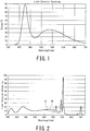
- Fig. 1 shows a light emission spectrum of a white light source described in Patent Document 1.
- Patent Document 2 discloses a white light source in which an ultraviolet light emitting diode and phosphors are combined.
- a white light source having high color rendering properties is realized by combining the ultraviolet light emitting diode and three types of phosphor, namely, a blue phosphor, a green phosphor, and a red phosphor, thereby to realize a white light source having a high color rendering property.
- Fig. 2 illustrates a light emission spectrum of the white light source described in Patent Document 2.
- a light emission peak in a red region is set so as to be high as shown in Fig. 2 .
- the color tones of an object of irradiation can be seen clearly.
- clothes or the like are illuminated, in some cases a significant difference may be perceived between the tones when the clothes or the like are irradiated with a white light source having high color rendering properties and the tones that are perceived under irradiation with sunlight.
- US-A1-2007/0235751 discloses a light emitting apparatus including a phosphor blend including two or more phosphors to provide an emission spectrum simulating the spectral power distribution of a CIE reference illuminant across at least a certain spectral range. Such an apparatus is particularly suited for color-critical applications.
- Human perception of the color of an object is a process in which a light from a light source is irradiated onto the object, and a reflected light from the object is perceived by a human.
- Spectral components of the reflected light can be expressed as the product of the light emission spectrum of the light source and the reflection spectrum of the object.
- Sunlight is also referred to as "black-body radiation”.
- Black-body radiation has a light emission spectrum that corresponds with a color temperature, and has a light emission spectrum without bumps and dips (irregularities).
- the spectrum of the reflected light also has bumps and dips that correspond to the bumps and dips in the light emission spectrum of the white light source. If the bumps and dips in the reflected light are large, the reflected light will lack a specific wavelength in the visible light region, and the appearance of the color of an object will change. That is, the problem arises that a divergence from the spectrum of black-body radiation increases because the bumps and dips of the light emission spectrum of the white light source are large, and consequently the way in which the tones are perceived differs.
- the present invention which has been made in order to deal with such a problem, has an object to provide a white light source with which the appearance of the color tones of an irradiation object are equivalent to the appearance of the tones when the object is irradiated with sunlight.
- the present invention provides a white light source according to Claim 1.
- the present invention also provides a white light source system according to Claim 12.
- a white light source reduces bumps and dips (irregularities) in a light emission spectrum, and hence the color tones of an object can be perceived in a similar manner to when the object is irradiated with sunlight.
- a white light source is a white light source including a light emitting diode having a light emission peak wavelength equal to or greater than 350 nm and less than or equal to 490 nm and a phosphor that emits visible light upon excitation by a light emitted from the light emitting diode, in which, with respect to an arbitrary local maximum value of light-emission intensity between 350 and 780 nm of a light emission spectrum of the white light source, a ratio of a local minimum value of light-emission intensity that is closest on a long wavelength side to the local maximum value is such that, when the local maximum value is taken as 1, the local minimum value is 0.5 or more.
- the following light emitting diodes are used as a light emitting diode having a light emission peak wavelength equal to or greater than 350 nm and less than or equal to 490 nm. That is, a light emitting diode (LED) that emits so-called ultraviolet light, violet light or blue light is used. Light emitting diodes that have a light emission peak in this region are suitable for exciting phosphors, and white light can be obtained by using various phosphors that are described later.
- LED light emitting diode
- a feature of the white light source according to the present invention is that with respect to an arbitrary local maximum value of light-emission intensity between 350 and 780 nm of a light emission spectrum of the white light source, a ratio of a local minimum value of light-emission intensity that is closest on a long wavelength side to the local maximum value is such that, when the local maximum value is taken as 1, the local minimum value is 0.5 or more.
- the light emission spectrum of the white light source is measured according to total luminous flux measurement using an integrating sphere in conformity with JIS-C-8152.
- a feature according to the present invention is that if a local maximum value of light-emission intensity and also a local minimum value of light-emission intensity that is closest to the local maximum value of light-emission intensity exist in the light emission spectrum of the white light source, the local maximum value of light-emission intensity is taken as 1, and a ratio between the local maximum value and the local minimum value (peak height of local minimum value of light-emission intensity/peak height of local maximum value of light-emission intensity) is 0.5 or more.
- local maximum value of light-emission intensity refers to a maximum value of a portion at which the light emission spectrum exhibits a mountain shape. That is, the local maximum value shows a maximum value in a mountain shape that rises and falls.
- local minimum value of light-emission intensity shows a minimum value of a portion at which the light emission spectrum exhibits a valley shape. That is, the local minimum value is a minimum value in a valley shape that falls and rises.
- a value in the case of a portion that continues rising in a gently-sloping manner (including a parallel manner), that is, a portion which includes no falling portion, is not referred to as a local maximum value.
- a value in the case of a portion that continues falling in a gently-sloping manner (including a parallel manner), that is, a portion which includes no rising portion is not referred to as a local minimum value.
- a feature according to the present invention is that, when a peak height of an arbitrary local maximum value is taken as 1, with regard to a local minimum value that is closest on a long wavelength side of the local maximum value, a ratio between the local maximum value and the local minimum value (peak height of local minimum value/peak height of local maximum value) is 0.5 or more.
- an intensity ratio is defined with respect to a portion at which a local maximum value and a local minimum value are closest to each other in a light emission spectrum, and an intensity ratio is not limited with regard to a portion at which even though there is a local maximum value there is no local minimum value that is closest thereto on a long wavelength side.
- a ratio of a local minimum value of light-emission intensity that is closest on a long wavelength side to the local maximum value is such that, when the local maximum value is taken as 1, the local minimum value is 0.7 or more. Note that although a limit of the ratio between a local maximum value and a local minimum value that is closest thereto on the long wavelength side is 1, a limit of 0.95 or less is preferable in consideration of manufacturability.
- Fig. 3 is a view illustrating a light emission spectrum according to Example 1 that is described later.
- the maximum peak intensity is present at a wavelength of 635 nm.
- the only portion having a local maximum value and a local minimum value that is closest thereto on the long wavelength side thereof is a portion including a local maximum value P1 (409 nm) and a local minimum value P2 (429 nm).
- the color temperature of the white light is between 2,500 and 7,000 K. If this color temperature falls below 2,500 K or exceeds 7,000 K, a color temperature that does not exist in sunlight may be unfavorably produced.
- the preferable range of the color temperature is 2,700 to 6,700 K. It is possible to adjust the color temperature by means of the mixing ratio of the phosphors of the respective colors. The color temperature is calculated from the light emission spectrum. Note that the unit of the color temperature is kelvin (K).
- the maximum peak intensity is within a range of 491 to 780 m. If the maximum peak intensity is within the range of 491 to 780 m, it means that there is no maximum peak in a region ranging from 350 to 490 nm. It has been reported in recent research that blue light causes Asian (including Japanese) and European people to feel a relatively dazzling sensation. It has also been reported that prolonged exposure to blue light results into adverse influences on the human body. For example, problems include retinopathy and sleeping disorders caused by suppression of melatonin secretion. Further, several adverse effects on humans have been similarly reported with respect to prolonged exposure to ultraviolet light. Therefore, adverse effects on humans can be suppressed when there is no maximum peak in a region ranging from an ultraviolet to blue region.
- the white light source of the present invention with respect to a black-body radiation spectrum having the same color temperature as that of the white light source, in a case where the black-body radiation spectrum when a visual luminance is made identical to that of the white light source is compared with the light emission spectrum of the white light source, the maximum light emission intensity of the light emission spectrum of a violet to blue region (380 to 490 nm) of the white light source is an intensity that is less than or equal to 1.5 times the light emission intensity of the black-body radiation spectrum at the same wavelength as the wavelength exhibiting the maximum light emission intensity.
- the intensity ratio is 1.5 or less, the spectral distribution of the white light source can be regarded as being close to that of sunlight, and humans do not feel discomfort from this light source.
- the smaller that the value of the intensity ratio is the better if the value is extremely small a problem will arise that a blue component of the light source will excessively decrease and the appearance of the object will become unnatural. Therefore, it is desirable that blue light of a certain intensity or more is also included, and thus a more desirable range of the intensity ratio is from 0.8 to 1.2.
- each phosphor is not particularly limited as long as the material emits visible light upon excitation by light emitted from a light emitting diode, it is preferable that a peak wavelength of each phosphor is in a range of 420 to 700 nm.
- the white light source includes three or more types, or furthermore, four or more types of phosphors each having different light emission peak wavelengths.
- a light emission peak of the light emitting diode is in a range of 350 to 420 nm, it is preferable to use four or more types of phosphor having different peak wavelengths.
- a light emission peak of the light emitting diode is in a range of 421 to 490 nm, it is preferable to use three or more types of phosphor having different peak wavelengths.
- the phosphors it is preferable to select phosphors of three or more types, or furthermore, four or more types from among blue phosphor, green phosphor, yellow phosphor and red phosphor.
- the white light source includes a phosphor for which the half-value width of the light emission spectrum is 50 nm or more.
- a phosphor having a broad light emission spectrum such that the half-value width of the light emission spectrum is 50 nm or more, it is easy to adjust the intensity ratio (local minimum value/local maximum value) between the local maximum value and local minimum value that are closest on the long wavelength side to 0.5 or more.
- a half-value width of the light emission spectrum of at least one type of phosphor is 50 nm or more, it is more preferable that the half-value width of two types, or furthermore, all three types of phosphor is 50 nm or more. It is also preferable that the limit of the half-value width is 100 nm or less.
- the white light source it preferable that there are at least one or more regions at which the light emission spectrums of the light emitting diode and the three or more types of phosphor having different light emission peak wavelengths overlap.
- a local maximum value and a local minimum value that are closest on the long wavelength side of the light emission spectrum of the white light source 0.5 or more, it is effective not to form a light emission intensity region that protrudes by itself in a visible light region, particularly in a region from 420 to 700 nm.
- the number of regions at which the light emission spectrums overlap is two or as high as three regions.
- each phosphor is not particularly limited, the following materials may be mentioned as materials that satisfy the foregoing conditions.
- blue phosphor (B) may include a europium-activated alkaline-earth phosphate phosphor (a peak wavelength of 440 to 455 nm) and a europium-activated barium magnesium aluminate phosphor (a peak wavelength of 450 to 460 nm).
- BG blue-green phosphor
- BG may include a europium-activated strontium aluminate phosphor (a peak wavelength of 480 to 500 nm) and a europium- and manganese-activated barium magnesium aluminate phosphor (a peak wavelength of 510 to 520 nm).
- green phosphor (G) may include a europium-activated orthosilicate phosphor (a peak wavelength of 520 to 550 nm), a europium-activated ⁇ -sialon phosphor (a peak wavelength of 535 to 545 nm), and a europium-activated strontium sialon phosphor (a peak wavelength of 510 to 530 nm).
- yellow phosphor (Y) may include a europium-activated orthosilicate phosphor (a peak wavelength of 550 to 580 nm) and a cerium-activated rare-earth aluminum garnet phosphor (a peak wavelength of 550 to 580 nm).
- red phosphor (R) may include a europium-activated strontium sialon phosphor (a peak wavelength of 600 to 650 nm), a europium-activated calcium strontium nitride phosphor (a peak wavelength of 610 to 650 nm), a europium-activated lanthanum oxysulfide phosphor (a peak wavelength of 620 to 630 nm), a manganese-activated magnesium fluorogermanate (a peak wavelength of 640 to 660 nm), and a europium-activated alkaline-earth nitride phosphor (a peak wavelength of 600 to 650 nm).
- a europium-activated strontium sialon phosphor a peak wavelength of 600 to 650 nm
- a europium-activated calcium strontium nitride phosphor a peak wavelength of 610 to 650 nm
- the average particle size of the phosphors is between 1 and 100 ⁇ m, and more preferably 5 and 50 ⁇ m.
- the average particle size is between 1 and 100 ⁇ m, and furthermore, it preferable that the average particle size is in a range of 5 to 50 ⁇ m.
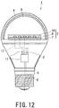
- Fig. 12 illustrates a bulb-type white light source as an example of one embodiment of the white light source according to the present invention.
- a reference numeral 1 denotes an LED bulb (white light source)
- reference numeral 2 denotes an LED module
- reference numeral 3 denotes a base body
- reference numeral 4 denotes a globe
- reference numeral 5 denotes an insulating member
- reference numeral 6 denotes a cap
- reference numeral 7 denotes a substrate
- reference numeral 8 denotes LED chips
- reference numeral 9 denotes a phosphor layer
- reference numeral 10 denotes a transparent resin layer.
- Fig. 12 illustrates an example of a structure in which a space is provided between a phosphor layer and a light emitting diode.
- the LED bulb 1 illustrated in Fig. 12 includes: the LED module 2; the base body 3 to which the LED module 2 is set; the globe 4 that is attached to an upper portion of the base body 3 so as to cover the LED module 2; the cap 6 that is attached to a lower end part of the base body 3 with the intermediation of the insulating member 5; and a lighting circuit 11 provided inside of the base body 3.
- the LED module 2 includes the LED chips 8 that emit light having a light emission peak wavelength between 350 and 490 nm that are mounted on the substrate 7.
- the plurality of LED chips 8 are surface-mounted on the substrate 7.
- InGaN-based, GaN-based, and AlGaN-based light emitting diodes are used for the LED chips 8.
- a wiring network (not illustrated) is provided on a surface of the substrate 7 (further provided inside thereof as needed), and an electrode of each LED chip 8 is electrically connected to the wiring network of the substrate 7.
- Wiring lines 12 are drawn from a side surface or a bottom surface of the LED module 2, and the wiring lines 12 are electrically connected to the lighting circuit 11 provided inside the base body 3.
- the LED chips 8 are turned on by DC voltage applied via the lighting circuit 11.
- the phosphor layer 9 that absorbs light emitted from the LED chips 8 and emits white light is provided on an inner surface of the globe 4.
- the phosphor layer 9 is formed by combining, as needed, three or more types, and furthermore, four or more types of phosphor having different peak wavelengths. Further, the phosphor layer 9 is formed by mixing the phosphors with a resin. Further, all the phosphors may be mixed to form a mixed phosphor layer. Alternatively, phosphor layers formed by mixing about one to three types of phosphor are laminated to form a multi-layer phosphor layer.
- Fig. 12 illustrates a structure in which the phosphor layer is provided on the inner surface of the globe 4, the phosphor layer may be provided on an outer surface of the globe 4, or the phosphors may be mixed in the resin-made globe 4 itself.
- the white light source according to the present invention is not limited to the above described bulb types, and the white light source can also be applied to a fluorescent light type (elongated type), a chandelier type, and the like, and the shape thereof is not limited.
- an LED chip 8a and a phosphor layer 9a, an LED chip 8b and a phosphor layer 9b, and an LED chip 8c and a phosphor layer 9c may be placed together on a common substrate 7. Then, the LED chips 8a, 8b, and 8c may be housed in the same globe 4, whereby a white light source system 1a may be configured. Further, a transparent resin layer may be provided between the LED chip 8 and the phosphor layer 9.
- the LED chips 8a, 8b, and 8c are each connected to a lighting circuit 11a by a wiring line 12a.
- a user can select an LED chip to be turned on by means of a switching mechanism (not illustrated) contained inside the lighting circuit 11a, as needed.
- the white light source according to the present invention can be applied to a structure in which a phosphor layer is provided on a light emitting diode, and also to a structure in which a phosphor layer is provided on a light emitting diode with the intermediation of a transparent resin layer. It is preferable that the thickness of the transparent resin layer is in a range of 0.01 to 0.1 mm.
- a structure in which a single phosphor layer is provided on a single LED chip (a one-chip type white light source), a structure may also be adopted in which a phosphor layer covers a plurality of LED chips (a multi-chip type white light source). Further, in the case of each of a bulb-type, a one-chip type, and a multi-chip type, it is preferable that the thickness of the phosphor layer is in a range of 0.01 to 3 mm. Furthermore, a plurality of white light sources may also be arranged to form a unit and used as a white light source system.
- the above described white light source according to the present invention is effective as a white light source that is used for task illumination.
- illumination for illuminating a wide area such as an entire room is defined as ambient illumination
- illumination for illuminating a comparatively narrow area such as around the hands of a worker when performing office work such as operating a personal computer is defined as task illumination.
- the recommended level of illuminance according to JIS-Z-9110 is between around 500 to 750 lux.
- the white light source is also effective for use in illumination for illuminating any one or more kinds among printed matter, foodstuff, and a human.
- printed matter refers to newspapers and magazines and the like.
- foodstuff includes all kinds of food and beverages.
- human refers mainly to the human face.
- the white light source is effective for illumination in a case where a distance from an object of irradiation (physical object) is 1.5 m or less.
- a distance from an object of irradiation physical object
- the color tones of an object can be perceived with color tones that are equivalent to those in a case where the object is illuminated with sunlight.
- the white light source does not have a light emission spectrum in which a specific wavelength protrudes, even if the distance from the object of irradiation is 1.5 m or less, or even approaches a distance of 1 m or less, the burden imposed on the eyes can be suppressed.
- the present invention is not limited thereto, and it is possible to use the white light source for various kinds of illumination.
- LED chips each having a light emission peak wavelength of 400 nm were prepared. Next, there was prepared a mixture including: a europium-activated alkaline-earth phosphate blue phosphor having a peak wavelength of 445 nm; a europium-activated strontium aluminate blue-green phosphor having a peak wavelength of 490 nm; a europium-activated orthosilicate green phosphor having a peak wavelength of 530 nm; a europium-activated orthosilicate yellow phosphor having a peak wavelength of 555 nm; and a europium-activated strontium sialon red phosphor having a peak wavelength of 630 nm, as phosphors that emitted light while being irradiated with electromagnetic waves of 400 nm.
- the average particle size of the phosphors was set to 18 ⁇ m.
- the correlated color temperature of light emission color of the obtained white light source was 2,800 K.
- phosphors for which a half-value width of the light emission spectrum was 50 nm or more were the blue-green phosphor, the green phosphor, the yellow phosphor, and the red phosphor. Further, with respect to the light emission spectrums of the blue phosphor, the blue-green phosphor, the green phosphor, the yellow phosphor, and the red phosphor, there was an overlapping portion in the light emission spectrums of the phosphors whose respective peak wavelengths were adjacent. The thickness of the phosphor layer was set to 0.4 mm.
- Fig. 3 shows a result obtained by measuring the light emission spectrum of the bulb-type white light source in Example 1 according to total luminous flux measurement using an integrating sphere in conformity with JIS-C-8152.
- ratios local minimum value/local maximum value between a local maximum value P1 and a local minimum value P2 that were adjacent on the long wavelength side were each 0.5 or more.
- LED chips each having a light emission peak wavelength of 400 nm were prepared. Next, there was prepared a mixture including: a europium-activated alkaline-earth phosphate blue phosphor having a peak wavelength of 445 nm; a europium-activated strontium aluminate blue-green phosphor having a peak wavelength of 490 nm; a europium-activated ⁇ -sialon green phosphor having a peak wavelength of 540 nm; a europium-activated orthosilicate yellow phosphor having a peak wavelength of 555 nm; and a europium-activated strontium sialon red phosphor having a peak wavelength of 630 nm, as phosphors that emitted light while being irradiated with electromagnetic waves of 400 nm.
- the average particle size of the phosphors was set to 13 ⁇ m.
- the correlated color temperature of light emission color of the obtained white light source was 2,800 K.
- phosphors for which a half-value width of the light emission spectrum was 50 nm or more were the blue-green phosphor, the green phosphor, the yellow phosphor, and the red phosphor. Further, with respect to the light emission spectrums of the blue phosphor, the blue-green phosphor, the green phosphor, the yellow phosphor, and the red phosphor, there was an overlapping portion in the light emission spectrums of the phosphors whose respective peak wavelengths were adjacent. The thickness of the phosphor layer was set to 0.2 mm.
- Fig. 4 shows the result thereof.
- ratios local minimum value/local maximum value between a local maximum value and a local minimum value that were adjacent on the long wavelength side were each 0.5 or more.
- LED chips each having a light emission peak wavelength of 400 nm were prepared. There was prepared a mixture including: a europium-activated alkaline-earth phosphate blue phosphor having a peak wavelength of 445 nm; a europium-activated strontium aluminate blue-green phosphor having a peak wavelength of 490 nm; a europium-activated orthosilicate green phosphor having a peak wavelength of 530 nm; a europium-activated orthosilicate yellow phosphor having a peak wavelength of 555 nm; and a europium-activated alkaline-earth nitride red phosphor having a peak wavelength of 635 nm, as the phosphors that emitted light while being irradiated with electromagnetic waves of 400 nm.
- the average particle size of the phosphors was set to 28 ⁇ m.
- the correlated color temperature of light emission color of the obtained white light source was 2,700 K.
- phosphors for which a half-value width of the light emission spectrum was 50 nm or more were the blue-green phosphor, the green phosphor, the yellow phosphor, and the red phosphor. Further, with respect to the light emission spectrums of the blue phosphor, the blue-green phosphor, the green phosphor, the yellow phosphor, and the red phosphor, there was an overlapping portion in the light emission spectrums of the phosphors whose respective peak wavelengths were adjacent. The thickness of the phosphor layer was set to 1.0 mm.
- Fig. 5 shows the result thereof.
- local maximum values and local minimum values that varied significantly were not observed, and ratios (local minimum value/local maximum value) between a local maximum value and a local minimum value that were adjacent on the long wavelength side were each 0.5 or more.
- LED chips each having a light emission peak wavelength of 400 nm were prepared. Next, there was prepared a mixture including: a europium-activated alkaline-earth phosphate blue phosphor having a peak wavelength of 445 nm; a europium-activated strontium aluminate blue-green phosphor having a peak wavelength of 490 nm; a europium-activated orthosilicate green phosphor having a peak wavelength of 530 nm; a europium-activated orthosilicate yellow phosphor having a peak wavelength of 555 nm; and a europium-activated strontium sialon red phosphor having a peak wavelength of 630 nm, as phosphors that emitted light while being irradiated with electromagnetic waves of 400 nm.
- the average particle size of the phosphors was set to 18 ⁇ m.
- the correlated color temperature of light emission color of the obtained white light source was 3,800 K.
- phosphors for which a half-value width of the light emission spectrum was 50 nm or more were the blue-green phosphor, the green phosphor, the yellow phosphor, and the red phosphor. Further, with respect to the light emission spectrums of the blue phosphor, the blue-green phosphor, the green phosphor, the yellow phosphor, and the red phosphor, there was an overlapping portion in the light emission spectrums of the phosphors whose respective peak wavelengths were adjacent. The thickness of the phosphor layer was set to 0.5 mm.
- Fig. 6 shows the result thereof.
- ratios local minimum value/local maximum value between a local maximum value and a local minimum value that were adjacent on the long wavelength side were each 0.5 or more.
- LED chips each having a light emission peak wavelength of 400 nm were prepared. Next, there was prepared a mixture including: a europium-activated alkaline-earth phosphate blue phosphor having a peak wavelength of 445 nm; a europium-activated strontium aluminate blue-green phosphor having a peak wavelength of 490 nm; a europium-activated ⁇ -sialon green phosphor having a peak wavelength of 540 nm; a europium-activated orthosilicate yellow phosphor having a peak wavelength of 555 nm; and a europium-activated strontium sialon red phosphor having a peak wavelength of 630 nm, as phosphors that emitted light while being irradiated with electromagnetic waves of 400 nm.
- the average particle size of the phosphors was set to 10 ⁇ m.
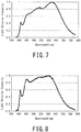
- Example 5 is a one-chip type white light source. The thickness of the phosphor layer was set to 0.3 mm. The correlated color temperature of light emission color of the obtained white light source was 4,200 K.
- phosphors for which a half-value width of the light emission spectrum was 50 nm or more were the blue-green phosphor, the green phosphor, the yellow phosphor, and the red phosphor. Further, with respect to the light emission spectrums of the blue phosphor, the blue-green phosphor, the green phosphor, the yellow phosphor, and the red phosphor, there was an overlapping portion in the light emission spectrums of the phosphors whose respective peak wavelengths were adjacent.
- Fig. 7 illustrates the result obtained when the light emission spectrum of the white light source of Example 5 was checked. As is apparent from Fig. 7 , ratios (local minimum value/local maximum value) between a local maximum value and a local minimum value that were adjacent on the long wavelength side were each 0.5 or more.
- LED chips each having a light emission peak wavelength of 400 nm were prepared. Next, there was prepared a mixture including: a europium-activated alkaline-earth phosphate blue phosphor having a peak wavelength of 445 nm; a europium-activated strontium aluminate blue-green phosphor having a peak wavelength of 490 nm; a europium-activated ⁇ -sialon green phosphor having a peak wavelength of 540 nm; a europium-activated orthosilicate yellow phosphor having a peak wavelength of 555 nm; and a europium-activated strontium sialon red phosphor having a peak wavelength of 630 nm, as phosphors that emitted light while being irradiated with electromagnetic waves of 400 nm.
- the average particle size of the phosphors was set to 10 ⁇ m.
- Example 6 is a one-chip type white light source. The thickness of the phosphor layer was set to 0.3 mm. The correlated color temperature of light emission color of the obtained white light source was 5,000 K.
- phosphors for which a half-value width of the light emission spectrum was 50 nm or more were the blue-green phosphor, the green phosphor, the yellow phosphor, and the red phosphor. Further, with respect to the light emission spectrums of the blue phosphor, the blue-green phosphor, the green phosphor, the yellow phosphor, and the red phosphor, there was an overlapping portion in the light emission spectrums of the phosphors whose respective peak wavelengths were adjacent.
- Fig. 8 illustrates the result obtained when the light emission spectrum of the white light source of Example 6 was checked. As is apparent from Fig. 8 , ratios (local minimum value/local maximum value) between a local maximum value and a local minimum value that were adjacent on the long wavelength side were each 0.5 or more.
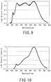
- LED chips each having a light emission peak wavelength of 400 nm were prepared. Next, there was prepared a mixture including: a europium-activated alkaline-earth phosphate blue phosphor having a peak wavelength of 445 nm; a europium-activated strontium aluminate blue-green phosphor having a peak wavelength of 490 nm; a europium-activated ⁇ -sialon green phosphor having a peak wavelength of 540 nm; a europium-activated orthosilicate yellow phosphor having a peak wavelength of 555 nm; and a europium-activated strontium sialon red phosphor having a peak wavelength of 630 nm, as phosphors that emitted light while being irradiated with electromagnetic waves of 400 nm.
- the average particle size of the phosphors was set to 13 ⁇ m.
- the correlated color temperature of light emission color of the obtained white light source was 5,000 K.
- phosphors for which a half-value width of the light emission spectrum was 50 nm or more were the blue-green phosphor, the green phosphor, the yellow phosphor, and the red phosphor. Further, with respect to the light emission spectrums of the blue phosphor, the blue-green phosphor, the green phosphor, the yellow phosphor, and the red phosphor, there was an overlapping portion in the light emission spectrums of the phosphors whose respective peak wavelengths were adjacent. The thickness of the phosphor layer was set to 0.2 mm.
- Fig. 9 shows the result thereof.
- ratios local minimum value/local maximum value between a local maximum value and a local minimum value that were adjacent on the long wavelength side were each 0.5 or more.
- a blue light emitting LED having a light emission peak wavelength of 445 nm was prepared as an LED chip. Next, there was prepared a mixture including: a europium-activated orthosilicate green phosphor having a peak wavelength of 530 nm; a europium-activated orthosilicate yellow phosphor having a peak wavelength of 530 nm; and a europium-activated strontium sialon red phosphor having a peak wavelength of 630 nm, as phosphors that emitted light while being irradiated with electromagnetic waves of 445 nm.
- the average particle size of the phosphors was set to 17 ⁇ m.
- the correlated color temperature of light emission color of the obtained white light source was 2,700 K.
- the thickness of the phosphor layer was set to 0.5 mm.
- phosphors for which a half-value width of the light emission spectrum was 50 nm or more were the green phosphor, the yellow phosphor, and the red phosphor. Further, with respect to the light emission spectrums of the green phosphor, the yellow phosphor, and the red phosphor, there was an overlapping portion in the light emission spectrums of the phosphors whose respective peak wavelengths were adjacent.
- Fig. 10 shows the result thereof.
- ratios local minimum value/local maximum value between a local maximum value and a local minimum value that were adjacent on the long wavelength side were each 0.5 or more.
- a blue light emitting LED having a light emission peak wavelength of 445 nm was prepared as an LED chip. Next, there was prepared a mixture including: a europium-activated orthosilicate green phosphor having a peak wavelength of 530 nm; a europium-activated orthosilicate yellow phosphor having a peak wavelength of 530 nm; and a europium-activated strontium sialon red phosphor having a peak wavelength of 630 nm, as phosphors that emitted light while being irradiated with electromagnetic waves of 445 nm.
- the average particle size of the phosphors was set to 15 ⁇ m.
- the correlated color temperature of light emission color of the obtained white light source was 2,700 K.
- the thickness of the phosphor layer was set to 0.4 mm.
- phosphors for which a half-value width of the light emission spectrum was 50 nm or more were the green phosphor, the yellow phosphor, and the red phosphor. Further, with respect to the light emission spectrums of the green phosphor, the yellow phosphor, and the red phosphor, there was an overlapping portion in the light emission spectrums of the phosphors whose respective peak wavelengths were adjacent.
- Fig. 11 shows the result thereof.
- ratios local minimum value/local maximum value between a local maximum value and a local minimum value that were adjacent on the long wavelength side were each 0.5 or more.
- Table 1 shows minimum value of ratios obtained in the above described Examples 1 to 9 in cases where, at the wavelengths between 350 to 780 nm, with respect to a local maximum value of the light emission intensity, there is a local minimum value of the light emission intensity that is closest to the local maximum value on the long wavelength side, and a ratio (local minimum value/local maximum value) of the local minimum value with respect to the local maximum value when the local maximum value is taken as 1 is determined.
- Example 2 0.53
- Example 3 0.94
- Example 4 0.53
- Example 5 0.81
- Example 6 0.73
- Example 8 0.74 Example 9 0.67
- a one-chip type white light source having the light emission spectrum illustrated in Fig. 1 was prepared as Comparative Example 1
- a one-chip type white light source having the light emission spectrum illustrated in Fig. 2 was prepared as Comparative Example 2.
- the respective light emission spectrums for Comparative Example 1 and Comparative Example 2 each included a portion at which a difference between a local maximum value and a local minimum value that were adjacent on the long wavelength side exceeded 0.5.
- the white light source exhibiting R9 as described above is suitable as a white light source that is used for task illumination, for illuminating any one or more kinds among printed matter, foodstuff, and a human, and for illumination when a distance to an object of irradiation is 1.5 m or less.
- light emission apparatuses white light sources
- respective examples and comparative examples were prepared as described below, and tests were conducted to check the influence on the human body of thus obtained light sources.
- a sensory evaluation was conducted with respect to whether or not people felt uncomfortable when exposed to light of the respective light sources at the same intensity of illumination.
- LED chips each having a light emission peak wavelength of 380 nm were prepared.
- a mixture including: a europium-activated alkaline-earth phosphate blue phosphor having a peak wavelength of 445 nm; a europium-activated strontium aluminate blue-green phosphor having a peak wavelength of 490 nm; a europium-activated ⁇ -sialon green phosphor having a peak wavelength of 540 nm; a europium-activated orthosilicate yellow phosphor having a peak wavelength of 555 nm; and a europium-activated strontium sialon red phosphor having a peak wavelength of 630 nm, as phosphors that emitted light while being irradiated with electromagnetic waves of 380 nm.
- the average particle size of the phosphors was set to 13 ⁇ m.
- Each phosphor mixture and silicone resin were mixed, and the resulting mixtures were then applied, respective, to the globe inner surface whereby a bulb-type white light source having the same structure as the white light source illustrated in Fig. 12 was manufactured.
- Table 3 a variety of white light sources for which the respective correlated color temperatures of light emission color were in a range of 2,800 K to 6,500 K were manufactured and used as Examples 10 to 18.
- Example 19 mixed phosphors were used in which the content of the blue phosphor component was made extremely small.
- mixed phosphors from which a phosphor component having a light emission peak in a blue region was removed were used as Example 20.
- the thickness of the phosphor layer in each example was set to 0.2 mm.
- the maximum intensity of light emission spectrums in a violet to blue region (380 to 490 nm) in visible light (380 nm to 780 nm) was measured, and the measured maximum intensity and the intensity of the black-body radiation spectrum at the same wavelength as the wavelength exhibiting the maximum intensity were compared.
- the light emission spectrums used for the comparison were as follows.
- An intensity ratio (A*/B*) was calculated for a region from 380 to 490 nm of the light emission spectrum A( ⁇ ), assuming that: a wavelength at which the spectrum intensity is a maximum is ⁇ *, the maximum intensity is A*, and the spectrum intensity of B( ⁇ ) at the wavelength ⁇ * is B*. Table 3 shows the calculation results.
- the bulb-type white light sources according to Examples 10 to 20 and Comparative Examples 3 to 4 were turned on in front of 100 subjects, and there was performed a sensory evaluation test regarding how the respective light sources were visually perceived.
- the subjects were selected by random sampling and comprised 10 men and 10 women in each of the age brackets of 10 to 25, 26 to 40, 41 to 55, 56 to 70, and 71 and over, who were requested to take part in the test.
- the subjects were asked to evaluate how each of the light sources was visually perceived by ranking the respective light sources into one of the following five grades: ⁇ comfortable, ⁇ not uncomfortable, ⁇ has an uncomfortable feeling, ⁇ uncomfortable, and ⁇ extremely uncomfortable.
- Table 3 shows a summary of the light emission characteristics and sensory evaluation results with respect to the white light sources according to Examples 10 to 20 and Comparative Examples 3 to 4. Note that, with respect to the method used to describe the results of the sensory evaluation test, the characteristic of the rank selected most among the evaluations of the 100 people is described. The number of respondents who selected the rank in question is shown in parentheses. [Table 3] Sample No. Color Temperature (K) Ratio (Local Minimum Value /Local Maximum Value) ⁇ (nm) Ratio (A*/B*) Visual Perception of Light Source Example 10 5000 0.55 450 1.70 Uncomfortable(45) Example 11 2800 0.60 490 1.56 Uncomfortable(35) Example 12 2800 0.
- Example 15 5000 0.90 455 1.15 Comfortable(32)
- Example 16 5200 0.70 470 1.12 Comfortable (40)
- Example 17 6500 0.85 450 1.10 Comfortable (38)
- Example 18 3000 0.85 490 1.10 Comfortable (43)
- Example 19 2800 0.98 490 1.05 Comfortable (48)
- Example 20 2900 0.90 490 0.95 Comfortable (51) Comparative Example 3 5000 0.30 450 2.47 Extremely Uncomfortable(36) Comparative Example 4 2800 0.20 448 2.03 Uncomfortable(52)
Landscapes
- Engineering & Computer Science (AREA)
- General Engineering & Computer Science (AREA)
- Physics & Mathematics (AREA)
- Microelectronics & Electronic Packaging (AREA)
- Spectroscopy & Molecular Physics (AREA)
- Optics & Photonics (AREA)
- Manufacturing & Machinery (AREA)
- Computer Hardware Design (AREA)
- Power Engineering (AREA)
- Led Device Packages (AREA)
- Non-Portable Lighting Devices Or Systems Thereof (AREA)
- Luminescent Compositions (AREA)
Claims (13)
- Weißlichtquelle zum Emittieren eines Weißlichts, umfassend: eine lichtemittierende Diode, die eine Lichtemissions-Spitzenwellenlänge von 350 bis 490 nm aufweist; und einen Leuchtstoff, der bei Erregung durch ein von der lichtemittierenden Diode emittiertes Licht sichtbares Licht emittiert,
wobei eine maximale Spitzenintensität des Lichtemissionsspektrums der Weißlichtquelle innerhalb eines Bereichs von 491 bis 780 nm liegt.
wobei in Bezug auf das Lichtemissionsspektrum der Weißlichtquelle und ein Lichtemissionsspektrum von Schwarzkörperstrahlung, die eine selbe Farbtemperatur aufweist wie diejenige der Weißlichtquelle, in einem Fall, in dem beide Lichtemissionsspektren verglichen werden, in einem Fall, in dem visuelle Leuchtdichten angeglichen werden, eine maximale Lichtemissionsintensität eines Lichtemissionsspektrums eines violetten bis blauen Bereichs (380 bis 490 nm) der Weißlichtquelle eine Intensität ist, die kleiner als oder gleich das 1,5-fache einer Lichtemissionsintensität des Schwarzkörperstrahlungsspektrums einer selben Wellenlänge wie einer Wellenlänge ist, die die maximale Lichtemissionsintensität aufweist; und
wobei in Bezug auf einen willkürlichen lokalen Lichtemissionsintensitäts-Maximalwert zwischen 350 und 780 nm eines Lichtemissionsspektrums der Weißlichtquelle ein Verhältnis eines lokalen Lichtemissionsintensitäts-Minimalwerts, der auf einer langwelligen Seite dem lokalen Maximalwert am nähesten liegt, derart ist, dass wenn der lokale Maximalwert als 1 genommen wird, der lokale Minimalwert 0,5 oder mehr beträgt. - Weißlichtquelle nach Anspruch 1, wobei in Bezug auf das Lichtemissionsspektrum der Weißlichtquelle und ein Lichtemissionsspektrum von Schwarzkörperstrahlung, die eine selbe Farbtemperatur aufweist wie diejenige der Weißlichtquelle, in einem Fall, in dem beide Lichtemissionsspektren verglichen werden, in einem Fall, in dem visuelle Leuchtdichten angeglichen werden, eine maximale Lichtemissionsintensität eines Lichtemissionsspektrums eines violetten bis blauen Bereichs (380 bis 490 nm) der Weißlichtquelle eine Intensität ist, die größer als das 0,8-fache und kleiner als das 1,2-fache einer Lichtemissionsintensität des Schwarzkörperstrahlungsspektrums einer selben Wellenlänge wie einer Wellenlänge ist, die die maximale Lichtemissionsintensität aufweist.
- Weißlichtquelle nach einem von Anspruch 1 bis Anspruch 2, wobei das Lichtemissionsspektrum des Weißlichts ein kontinuierliches Spektrum ohne Unterbrechung in sichtbarem Wellenlängenbereich von 380 bis 780 nm aufweist.
- Weißlichtquelle nach einem von Anspruch 1 bis Anspruch 3, wobei eine Farbtemperatur des Weißlichts zwischen 2.500 und 7.000 K liegt.
- Weißlichtquelle nach einem von Anspruch 1 bis Anspruch 4, die drei oder mehr Arten von Leuchtstoffen umfasst, welche unterschiedliche Lichtemissions-Spitzenwellenlängen aufweisen.
- Weißlichtquelle nach Anspruch 5, wobei der Leuchtstoff drei oder mehr Arten von Leuchtstoffen umfasst, die ausgewählt sind aus der Gruppe, bestehend aus einem blaulichtemittierenden Leuchtstoff, einem grünlichtemittierenden Leuchtstoff, einem gelblichtemittierenden Leuchtstoff und einem rotlichtemittierenden Leuchtstoff.
- Weißlichtquelle nach Anspruch 6, wobei der Leuchtstoff aus einem gemischten Leuchtstoff besteht, der mindestens vier Arten von Leuchtstoffen eines blaulichtemittierenden Leuchtstoffs, eines grünlichtemittierenden Leuchtstoffs, eines gelblichtemittierenden Leuchtstoffs und eines rotlichtemittierenden Leuchtstoffs enthält.
- Weißlichtquelle nach einem von Anspruch 1 bis Anspruch 7, wobei der Leuchtstoff mindestens Europium als einen Aktivator enthält.
- Weißlichtquelle nach einem von Anspruch 3 bis Anspruch 8, umfassend mindestens einen oder mehrere Bereiche, an denen sich Lichtemissionsspektren der lichtemittierenden Diode und drei oder mehr Arten von Leuchtstoffen, die unterschiedliche Lichtemissions-Spitzenwellenlängen aufweisen, überlappen.
- Weißlichtquelle nach einem von Anspruch 1 bis Anspruch 9, wobei die Weißlichtquelle eine Weißlichtquelle ist, die für Aufgabenbeleuchtung verwendet wird.
- Weißlichtquelle nach einem von Anspruch 1 bis Anspruch 10, wobei die Weißlichtquelle in Beleuchtung zum Beleuchten von einem oder mehreren aus Druckerzeugnissen, Lebensmitteln und einem Menschen als ein Bestrahlungsobjekt verwendet wird.
- Weißlichtquelle nach einem von Anspruch 1 bis Anspruch 11, wobei ein Abstand zwischen der Weißlichtquelle und einem Bestrahlungsobjekt 1,5 m oder weniger beträgt.
- Weißlichtquellensystem, umfassend eine Vielzahl von Weißlichtquellen nach einem von Anspruch 1 bis Anspruch 11.
Applications Claiming Priority (3)
| Application Number | Priority Date | Filing Date | Title |
|---|---|---|---|
| JP2011243992 | 2011-11-07 | ||
| PCT/JP2012/077087 WO2013069435A1 (ja) | 2011-11-07 | 2012-10-19 | 白色光源およびそれを用いた白色光源システム |
| EP12848603.2A EP2778507B1 (de) | 2011-11-07 | 2012-10-19 | Weisslichtquelle und weisslichtquellensystem mit einem gleichen |
Related Parent Applications (2)
| Application Number | Title | Priority Date | Filing Date |
|---|---|---|---|
| EP12848603.2A Division EP2778507B1 (de) | 2011-11-07 | 2012-10-19 | Weisslichtquelle und weisslichtquellensystem mit einem gleichen |
| EP12848603.2A Division-Into EP2778507B1 (de) | 2011-11-07 | 2012-10-19 | Weisslichtquelle und weisslichtquellensystem mit einem gleichen |
Publications (2)
| Publication Number | Publication Date |
|---|---|
| EP3483496A1 EP3483496A1 (de) | 2019-05-15 |
| EP3483496B1 true EP3483496B1 (de) | 2020-07-29 |
Family
ID=48289818
Family Applications (2)
| Application Number | Title | Priority Date | Filing Date |
|---|---|---|---|
| EP18212955.1A Active EP3483496B1 (de) | 2011-11-07 | 2012-10-19 | Weisslichtquelle und weisslichtquellensystem damit |
| EP12848603.2A Active EP2778507B1 (de) | 2011-11-07 | 2012-10-19 | Weisslichtquelle und weisslichtquellensystem mit einem gleichen |
Family Applications After (1)
| Application Number | Title | Priority Date | Filing Date |
|---|---|---|---|
| EP12848603.2A Active EP2778507B1 (de) | 2011-11-07 | 2012-10-19 | Weisslichtquelle und weisslichtquellensystem mit einem gleichen |
Country Status (5)
| Country | Link |
|---|---|
| US (1) | US9605815B2 (de) |
| EP (2) | EP3483496B1 (de) |
| JP (1) | JP6189217B2 (de) |
| CN (1) | CN104011457B (de) |
| WO (1) | WO2013069435A1 (de) |
Families Citing this family (39)
| Publication number | Priority date | Publication date | Assignee | Title |
|---|---|---|---|---|
| CN103597568B (zh) * | 2011-04-01 | 2016-08-17 | 纳晶科技股份有限公司 | 白光发光器件 |
| US9410664B2 (en) * | 2013-08-29 | 2016-08-09 | Soraa, Inc. | Circadian friendly LED light source |
| EP3770493B1 (de) | 2013-09-09 | 2023-06-07 | Savant Technologies LLC | Lichtquellen mit verbesserter farbpräferenz |
| JP2015060969A (ja) * | 2013-09-19 | 2015-03-30 | 日本電気硝子株式会社 | 発光装置 |
| JP2015082596A (ja) | 2013-10-23 | 2015-04-27 | 株式会社東芝 | 発光装置 |
| EP3064039B1 (de) | 2013-10-28 | 2020-05-13 | GE Lighting Solutions, LLC | Lampen für verbesserte optische aufhellung und farbpräferenz |
| WO2015072766A1 (ko) * | 2013-11-13 | 2015-05-21 | 엘지이노텍(주) | 청녹색 형광체, 이를 포함하는 발광 소자 패키지 및 조명 장치 |
| JP6233750B2 (ja) * | 2014-03-14 | 2017-11-22 | パナソニックIpマネジメント株式会社 | 発光装置およびその製造方法、照明用光源、並びに照明装置 |
| US9992842B2 (en) * | 2014-12-01 | 2018-06-05 | Industrial Technology Research Institute | Illumination system and method for developing target visual perception of an object |
| KR102071954B1 (ko) | 2015-06-24 | 2020-01-31 | 가부시끼가이샤 도시바 | 백색 광원 시스템 |
| JP6490556B2 (ja) * | 2015-10-15 | 2019-03-27 | パラマウントベッド株式会社 | 照明装置 |
| EP3367448B1 (de) * | 2015-10-20 | 2021-04-28 | Kyocera Corporation | Innenraumlichtquelle und beleuchtungsvorrichtung |
| US9859470B2 (en) | 2016-03-10 | 2018-01-02 | Epistar Corporation | Light-emitting device with adjusting element |
| US10784416B2 (en) * | 2016-03-24 | 2020-09-22 | Sharp Kabushiki Kaisha | Light source device and light emitting device |
| JP6726882B2 (ja) * | 2017-01-25 | 2020-07-22 | パナソニックIpマネジメント株式会社 | 照明装置 |
| US10325963B2 (en) * | 2017-02-24 | 2019-06-18 | Innolux Corporation | Display device |
| TWI636286B (zh) * | 2017-03-31 | 2018-09-21 | 友達光電股份有限公司 | 顯示裝置 |
| US10056530B1 (en) * | 2017-07-31 | 2018-08-21 | Eie Materials, Inc. | Phosphor-converted white light emitting diodes having narrow-band green phosphors |
| KR101809098B1 (ko) * | 2017-08-14 | 2018-01-18 | 루미마이크로 주식회사 | 발광장치 |
| US10177287B1 (en) | 2017-09-19 | 2019-01-08 | Eie Materials, Inc. | Gamut broadened displays with narrow band green phosphors |
| JP6940764B2 (ja) * | 2017-09-28 | 2021-09-29 | 日亜化学工業株式会社 | 発光装置 |
| KR102541393B1 (ko) * | 2017-11-30 | 2023-06-09 | 삼성전자주식회사 | 디스플레이 장치 |
| JP6773018B2 (ja) * | 2017-12-26 | 2020-10-21 | 日亜化学工業株式会社 | 発光装置 |
| US11217725B2 (en) | 2018-02-26 | 2022-01-04 | Biological Innovation And Optimization Systems, Llc | Light emitting apparatus with melanopic emission spectrum |
| WO2019182195A1 (ko) * | 2018-03-21 | 2019-09-26 | 주식회사 올릭스 | 여기광을 제어한 형광체 파장 변환 백색 발광 소자 및 이를 포함하는 발광장치 |
| KR101990475B1 (ko) * | 2018-03-21 | 2019-06-19 | (주)올릭스 | 발광 스펙트럼을 제어한 초고연색 백색 발광 소자 및 이를 포함하는 조명 장치 |
| US11213693B2 (en) * | 2018-04-27 | 2022-01-04 | Seoul Viosys Co., Ltd. | Light source for eye therapy and light emitting device having the same |
| US10174242B1 (en) | 2018-05-17 | 2019-01-08 | Eie Materials, Inc. | Coated thioaluminate phosphor particles |
| US10236422B1 (en) | 2018-05-17 | 2019-03-19 | Eie Materials, Inc. | Phosphors with narrow green emission |
| CN108767097B (zh) * | 2018-05-31 | 2019-05-07 | 旭宇光电(深圳)股份有限公司 | 紫外激发全光谱led及其应用 |
| US10685941B1 (en) | 2019-07-09 | 2020-06-16 | Intematix Corporation | Full spectrum white light emitting devices |
| US10371325B1 (en) | 2018-06-25 | 2019-08-06 | Intematix Corporation | Full spectrum white light emitting devices |
| KR20200024607A (ko) | 2018-08-28 | 2020-03-09 | 주식회사 올릭스 | 식물생장용 광합성 클로로필 파장 변환 백색 발광 소자 및 조명장치 |
| KR20200024605A (ko) | 2018-08-28 | 2020-03-09 | 주식회사 올릭스 | 박물관 조명용 형광체 파장 변환 led 소자 및 조명장치 |
| CN109411456A (zh) * | 2018-10-16 | 2019-03-01 | 江苏稳润光电科技有限公司 | 一种用于生鲜灯照明的led光源 |
| US11125930B2 (en) * | 2018-12-17 | 2021-09-21 | Innolux Corporation | Lighting device |
| CN111755429B (zh) | 2019-03-29 | 2024-07-09 | 日亚化学工业株式会社 | 发光装置 |
| US11887973B2 (en) | 2019-07-09 | 2024-01-30 | Intematix Corporation | Full spectrum white light emitting devices |
| KR20240108728A (ko) | 2023-01-02 | 2024-07-09 | 유한회사 세미 | 의약용 대마 광합성 효율 향상을 위한 클로로필 파장 변환 led 조명장치 |
Family Cites Families (15)
| Publication number | Priority date | Publication date | Assignee | Title |
|---|---|---|---|---|
| JP2927279B2 (ja) | 1996-07-29 | 1999-07-28 | 日亜化学工業株式会社 | 発光ダイオード |
| US6853151B2 (en) * | 2002-11-19 | 2005-02-08 | Denovo Lighting, Llc | LED retrofit lamp |
| EP1644985A4 (de) | 2003-06-24 | 2006-10-18 | Gelcore Llc | Vollspektrum-leuchtstoffmischungen für die weisslichterzeugung mit led-chips |
| US7267787B2 (en) * | 2004-08-04 | 2007-09-11 | Intematix Corporation | Phosphor systems for a white light emitting diode (LED) |
| JP5398141B2 (ja) | 2005-09-29 | 2014-01-29 | 株式会社東芝 | 白色発光型ledランプおよびそれを用いたバックライト並びに液晶表示装置 |
| JP2007266579A (ja) * | 2006-02-28 | 2007-10-11 | Toshiba Lighting & Technology Corp | 発光装置 |
| KR100756465B1 (ko) * | 2006-04-17 | 2007-09-07 | 엘지전자 주식회사 | 냉장고용 야채실 조명구조 |
| JP2009065137A (ja) * | 2007-08-09 | 2009-03-26 | Toshiba Lighting & Technology Corp | 発光装置 |
| US8567973B2 (en) * | 2008-03-07 | 2013-10-29 | Intematix Corporation | Multiple-chip excitation systems for white light emitting diodes (LEDs) |
| TW201010125A (en) | 2008-08-22 | 2010-03-01 | Univ Nat Taiwan Science Tech | White light light-emitting diodes |
| JP4869317B2 (ja) * | 2008-10-29 | 2012-02-08 | 株式会社東芝 | 赤色蛍光体およびそれを用いた発光装置 |
| JP5005013B2 (ja) | 2009-09-16 | 2012-08-22 | 三菱電機株式会社 | 発光装置及び照明装置 |
| US20110220920A1 (en) | 2010-03-09 | 2011-09-15 | Brian Thomas Collins | Methods of forming warm white light emitting devices having high color rendering index values and related light emitting devices |
| EP3683494A1 (de) | 2011-02-09 | 2020-07-22 | Kabushiki Kaisha Toshiba | Weisslichtquelle und weisslichtquellensystem damit |
| EP3848985B1 (de) | 2011-04-22 | 2023-06-07 | Seoul Semiconductor Co., Ltd. | Weisslichtequipment |
-
2012
- 2012-10-19 WO PCT/JP2012/077087 patent/WO2013069435A1/ja active Application Filing
- 2012-10-19 JP JP2013542908A patent/JP6189217B2/ja active Active
- 2012-10-19 US US14/356,275 patent/US9605815B2/en active Active
- 2012-10-19 EP EP18212955.1A patent/EP3483496B1/de active Active
- 2012-10-19 CN CN201280054549.8A patent/CN104011457B/zh active Active
- 2012-10-19 EP EP12848603.2A patent/EP2778507B1/de active Active
Non-Patent Citations (1)
| Title |
|---|
| None * |
Also Published As
| Publication number | Publication date |
|---|---|
| EP3483496A1 (de) | 2019-05-15 |
| US20140307417A1 (en) | 2014-10-16 |
| EP2778507A4 (de) | 2015-08-05 |
| WO2013069435A1 (ja) | 2013-05-16 |
| JPWO2013069435A1 (ja) | 2015-04-02 |
| CN104011457A (zh) | 2014-08-27 |
| US9605815B2 (en) | 2017-03-28 |
| CN104011457B (zh) | 2016-08-24 |
| EP2778507B1 (de) | 2019-10-02 |
| JP6189217B2 (ja) | 2017-08-30 |
| EP2778507A1 (de) | 2014-09-17 |
Similar Documents
| Publication | Publication Date | Title |
|---|---|---|
| EP3483496B1 (de) | Weisslichtquelle und weisslichtquellensystem damit | |
| JP6763071B2 (ja) | 白色発光装置および照明装置 | |
| JP6567112B2 (ja) | 照明方法及び発光装置 | |
| US10957826B2 (en) | White light source including LED and phosphors | |
| JP2020198309A (ja) | 発光装置及びled電球 | |
| CN103299718B (zh) | 照明方法和发光装置 | |
| US9112120B2 (en) | White light source and white light source system including the same | |
| JP6820064B2 (ja) | 半導体発光素子を含む発光装置、発光装置の設計方法、発光装置の駆動方法、および照明方法 | |
| JP2015061009A (ja) | 光源装置 | |
| JP6584591B2 (ja) | 発光装置及び発光装置の設計方法 | |
| JP7486004B2 (ja) | 発光装置及びそれを備えた灯具 | |
| WO2021256307A1 (ja) | 照明装置 | |
| JP2016054044A (ja) | 半導体発光素子を含む発光装置、発光装置の設計方法、発光装置の駆動方法、および照明方法 |
Legal Events
| Date | Code | Title | Description |
|---|---|---|---|
| PUAI | Public reference made under article 153(3) epc to a published international application that has entered the european phase |
Free format text: ORIGINAL CODE: 0009012 |
|
| STAA | Information on the status of an ep patent application or granted ep patent |
Free format text: STATUS: REQUEST FOR EXAMINATION WAS MADE |
|
| 17P | Request for examination filed |
Effective date: 20181217 |
|
| AC | Divisional application: reference to earlier application |
Ref document number: 2778507 Country of ref document: EP Kind code of ref document: P |
|
| AK | Designated contracting states |
Kind code of ref document: A1 Designated state(s): AL AT BE BG CH CY CZ DE DK EE ES FI FR GB GR HR HU IE IS IT LI LT LU LV MC MK MT NL NO PL PT RO RS SE SI SK SM TR |
|
| GRAP | Despatch of communication of intention to grant a patent |
Free format text: ORIGINAL CODE: EPIDOSNIGR1 |
|
| STAA | Information on the status of an ep patent application or granted ep patent |
Free format text: STATUS: GRANT OF PATENT IS INTENDED |
|
| RIC1 | Information provided on ipc code assigned before grant |
Ipc: F21V 3/04 20180101ALI20200220BHEP Ipc: F21S 2/00 20160101AFI20200220BHEP Ipc: H01L 33/50 20100101ALI20200220BHEP Ipc: H01L 25/075 20060101ALN20200220BHEP Ipc: F21K 99/00 20160101ALI20200220BHEP |
|
| INTG | Intention to grant announced |
Effective date: 20200320 |
|
| RIC1 | Information provided on ipc code assigned before grant |
Ipc: F21S 2/00 20160101AFI20200310BHEP Ipc: F21K 99/00 20160101ALI20200310BHEP Ipc: H01L 25/075 20060101ALN20200310BHEP Ipc: F21V 3/04 20180101ALI20200310BHEP Ipc: H01L 33/50 20100101ALI20200310BHEP |
|
| GRAS | Grant fee paid |
Free format text: ORIGINAL CODE: EPIDOSNIGR3 |
|
| GRAA | (expected) grant |
Free format text: ORIGINAL CODE: 0009210 |
|
| STAA | Information on the status of an ep patent application or granted ep patent |
Free format text: STATUS: THE PATENT HAS BEEN GRANTED |
|
| RAP1 | Party data changed (applicant data changed or rights of an application transferred) |
Owner name: KABUSHIKI KAISHA TOSHIBA Owner name: TOSHIBA MATERIALS CO., LTD. |
|
| AC | Divisional application: reference to earlier application |
Ref document number: 2778507 Country of ref document: EP Kind code of ref document: P |
|
| AK | Designated contracting states |
Kind code of ref document: B1 Designated state(s): AL AT BE BG CH CY CZ DE DK EE ES FI FR GB GR HR HU IE IS IT LI LT LU LV MC MK MT NL NO PL PT RO RS SE SI SK SM TR |
|
| REG | Reference to a national code |
Ref country code: CH Ref legal event code: EP |
|
| REG | Reference to a national code |
Ref country code: AT Ref legal event code: REF Ref document number: 1296219 Country of ref document: AT Kind code of ref document: T Effective date: 20200815 |
|
| REG | Reference to a national code |
Ref country code: IE Ref legal event code: FG4D |
|
| REG | Reference to a national code |
Ref country code: DE Ref legal event code: R096 Ref document number: 602012071575 Country of ref document: DE |
|
| REG | Reference to a national code |
Ref country code: NL Ref legal event code: FP |
|
| REG | Reference to a national code |
Ref country code: LT Ref legal event code: MG4D |
|
| REG | Reference to a national code |
Ref country code: AT Ref legal event code: MK05 Ref document number: 1296219 Country of ref document: AT Kind code of ref document: T Effective date: 20200729 |
|
| PG25 | Lapsed in a contracting state [announced via postgrant information from national office to epo] |
Ref country code: HR Free format text: LAPSE BECAUSE OF FAILURE TO SUBMIT A TRANSLATION OF THE DESCRIPTION OR TO PAY THE FEE WITHIN THE PRESCRIBED TIME-LIMIT Effective date: 20200729 Ref country code: SE Free format text: LAPSE BECAUSE OF FAILURE TO SUBMIT A TRANSLATION OF THE DESCRIPTION OR TO PAY THE FEE WITHIN THE PRESCRIBED TIME-LIMIT Effective date: 20200729 Ref country code: PT Free format text: LAPSE BECAUSE OF FAILURE TO SUBMIT A TRANSLATION OF THE DESCRIPTION OR TO PAY THE FEE WITHIN THE PRESCRIBED TIME-LIMIT Effective date: 20201130 Ref country code: FI Free format text: LAPSE BECAUSE OF FAILURE TO SUBMIT A TRANSLATION OF THE DESCRIPTION OR TO PAY THE FEE WITHIN THE PRESCRIBED TIME-LIMIT Effective date: 20200729 Ref country code: LT Free format text: LAPSE BECAUSE OF FAILURE TO SUBMIT A TRANSLATION OF THE DESCRIPTION OR TO PAY THE FEE WITHIN THE PRESCRIBED TIME-LIMIT Effective date: 20200729 Ref country code: GR Free format text: LAPSE BECAUSE OF FAILURE TO SUBMIT A TRANSLATION OF THE DESCRIPTION OR TO PAY THE FEE WITHIN THE PRESCRIBED TIME-LIMIT Effective date: 20201030 Ref country code: AT Free format text: LAPSE BECAUSE OF FAILURE TO SUBMIT A TRANSLATION OF THE DESCRIPTION OR TO PAY THE FEE WITHIN THE PRESCRIBED TIME-LIMIT Effective date: 20200729 Ref country code: NO Free format text: LAPSE BECAUSE OF FAILURE TO SUBMIT A TRANSLATION OF THE DESCRIPTION OR TO PAY THE FEE WITHIN THE PRESCRIBED TIME-LIMIT Effective date: 20201029 Ref country code: BG Free format text: LAPSE BECAUSE OF FAILURE TO SUBMIT A TRANSLATION OF THE DESCRIPTION OR TO PAY THE FEE WITHIN THE PRESCRIBED TIME-LIMIT Effective date: 20201029 Ref country code: ES Free format text: LAPSE BECAUSE OF FAILURE TO SUBMIT A TRANSLATION OF THE DESCRIPTION OR TO PAY THE FEE WITHIN THE PRESCRIBED TIME-LIMIT Effective date: 20200729 |
|
| PG25 | Lapsed in a contracting state [announced via postgrant information from national office to epo] |
Ref country code: IS Free format text: LAPSE BECAUSE OF FAILURE TO SUBMIT A TRANSLATION OF THE DESCRIPTION OR TO PAY THE FEE WITHIN THE PRESCRIBED TIME-LIMIT Effective date: 20201129 Ref country code: PL Free format text: LAPSE BECAUSE OF FAILURE TO SUBMIT A TRANSLATION OF THE DESCRIPTION OR TO PAY THE FEE WITHIN THE PRESCRIBED TIME-LIMIT Effective date: 20200729 Ref country code: RS Free format text: LAPSE BECAUSE OF FAILURE TO SUBMIT A TRANSLATION OF THE DESCRIPTION OR TO PAY THE FEE WITHIN THE PRESCRIBED TIME-LIMIT Effective date: 20200729 Ref country code: LV Free format text: LAPSE BECAUSE OF FAILURE TO SUBMIT A TRANSLATION OF THE DESCRIPTION OR TO PAY THE FEE WITHIN THE PRESCRIBED TIME-LIMIT Effective date: 20200729 |
|
| PG25 | Lapsed in a contracting state [announced via postgrant information from national office to epo] |
Ref country code: DK Free format text: LAPSE BECAUSE OF FAILURE TO SUBMIT A TRANSLATION OF THE DESCRIPTION OR TO PAY THE FEE WITHIN THE PRESCRIBED TIME-LIMIT Effective date: 20200729 Ref country code: CZ Free format text: LAPSE BECAUSE OF FAILURE TO SUBMIT A TRANSLATION OF THE DESCRIPTION OR TO PAY THE FEE WITHIN THE PRESCRIBED TIME-LIMIT Effective date: 20200729 Ref country code: RO Free format text: LAPSE BECAUSE OF FAILURE TO SUBMIT A TRANSLATION OF THE DESCRIPTION OR TO PAY THE FEE WITHIN THE PRESCRIBED TIME-LIMIT Effective date: 20200729 Ref country code: EE Free format text: LAPSE BECAUSE OF FAILURE TO SUBMIT A TRANSLATION OF THE DESCRIPTION OR TO PAY THE FEE WITHIN THE PRESCRIBED TIME-LIMIT Effective date: 20200729 Ref country code: SM Free format text: LAPSE BECAUSE OF FAILURE TO SUBMIT A TRANSLATION OF THE DESCRIPTION OR TO PAY THE FEE WITHIN THE PRESCRIBED TIME-LIMIT Effective date: 20200729 |
|
| REG | Reference to a national code |
Ref country code: DE Ref legal event code: R097 Ref document number: 602012071575 Country of ref document: DE |
|
| PG25 | Lapsed in a contracting state [announced via postgrant information from national office to epo] |
Ref country code: AL Free format text: LAPSE BECAUSE OF FAILURE TO SUBMIT A TRANSLATION OF THE DESCRIPTION OR TO PAY THE FEE WITHIN THE PRESCRIBED TIME-LIMIT Effective date: 20200729 |
|
| REG | Reference to a national code |
Ref country code: CH Ref legal event code: PL |
|
| PLBE | No opposition filed within time limit |
Free format text: ORIGINAL CODE: 0009261 |
|
| STAA | Information on the status of an ep patent application or granted ep patent |
Free format text: STATUS: NO OPPOSITION FILED WITHIN TIME LIMIT |
|
| PG25 | Lapsed in a contracting state [announced via postgrant information from national office to epo] |
Ref country code: LU Free format text: LAPSE BECAUSE OF NON-PAYMENT OF DUE FEES Effective date: 20201019 Ref country code: MC Free format text: LAPSE BECAUSE OF FAILURE TO SUBMIT A TRANSLATION OF THE DESCRIPTION OR TO PAY THE FEE WITHIN THE PRESCRIBED TIME-LIMIT Effective date: 20200729 Ref country code: SK Free format text: LAPSE BECAUSE OF FAILURE TO SUBMIT A TRANSLATION OF THE DESCRIPTION OR TO PAY THE FEE WITHIN THE PRESCRIBED TIME-LIMIT Effective date: 20200729 |
|
| 26N | No opposition filed |
Effective date: 20210430 |
|
| REG | Reference to a national code |
Ref country code: DE Ref legal event code: R081 Ref document number: 602012071575 Country of ref document: DE Owner name: SEOUL SEMICONDUCTOR CO., LTD., ANSAN-SI, KR Free format text: FORMER OWNERS: KABUSHIKI KAISHA TOSHIBA, TOKYO, JP; TOSHIBA MATERIALS CO., LTD., YOKOHAMA-SHI, KANAGAWA, JP Ref country code: DE Ref legal event code: R082 Ref document number: 602012071575 Country of ref document: DE Representative=s name: HOFFMANN - EITLE PATENT- UND RECHTSANWAELTE PA, DE Ref country code: DE Ref legal event code: R081 Ref document number: 602012071575 Country of ref document: DE Owner name: TOSHIBA MATERIALS CO., LTD., YOKOHAMA-SHI, JP Free format text: FORMER OWNERS: KABUSHIKI KAISHA TOSHIBA, TOKYO, JP; TOSHIBA MATERIALS CO., LTD., YOKOHAMA-SHI, KANAGAWA, JP |
|
| REG | Reference to a national code |
Ref country code: BE Ref legal event code: MM Effective date: 20201031 |
|
| PG25 | Lapsed in a contracting state [announced via postgrant information from national office to epo] |
Ref country code: BE Free format text: LAPSE BECAUSE OF NON-PAYMENT OF DUE FEES Effective date: 20201031 Ref country code: CH Free format text: LAPSE BECAUSE OF NON-PAYMENT OF DUE FEES Effective date: 20201031 Ref country code: LI Free format text: LAPSE BECAUSE OF NON-PAYMENT OF DUE FEES Effective date: 20201031 Ref country code: SI Free format text: LAPSE BECAUSE OF FAILURE TO SUBMIT A TRANSLATION OF THE DESCRIPTION OR TO PAY THE FEE WITHIN THE PRESCRIBED TIME-LIMIT Effective date: 20200729 |
|
| REG | Reference to a national code |
Ref country code: GB Ref legal event code: 732E Free format text: REGISTERED BETWEEN 20210812 AND 20210818 |
|
| REG | Reference to a national code |
Ref country code: NL Ref legal event code: PD Owner name: TOSHIBA MATERIALS CO., LTD.; JP Free format text: DETAILS ASSIGNMENT: CHANGE OF OWNER(S), ASSIGNMENT; FORMER OWNER NAME: TOSHIBA MATERIALS CO., LTD. Effective date: 20210831 |
|
| PG25 | Lapsed in a contracting state [announced via postgrant information from national office to epo] |
Ref country code: IE Free format text: LAPSE BECAUSE OF NON-PAYMENT OF DUE FEES Effective date: 20201019 |
|
| REG | Reference to a national code |
Ref country code: NL Ref legal event code: PD Owner name: SEOUL SEMICONDUCTOR CO.,LTD.; KO Free format text: DETAILS ASSIGNMENT: CHANGE OF OWNER(S), ASSIGNMENT; FORMER OWNER NAME: TOSHIBA MATERIALS CO., LTD. Effective date: 20211207 |
|
| REG | Reference to a national code |
Ref country code: GB Ref legal event code: 732E Free format text: REGISTERED BETWEEN 20220224 AND 20220302 |
|
| PG25 | Lapsed in a contracting state [announced via postgrant information from national office to epo] |
Ref country code: TR Free format text: LAPSE BECAUSE OF FAILURE TO SUBMIT A TRANSLATION OF THE DESCRIPTION OR TO PAY THE FEE WITHIN THE PRESCRIBED TIME-LIMIT Effective date: 20200729 Ref country code: MT Free format text: LAPSE BECAUSE OF FAILURE TO SUBMIT A TRANSLATION OF THE DESCRIPTION OR TO PAY THE FEE WITHIN THE PRESCRIBED TIME-LIMIT Effective date: 20200729 Ref country code: CY Free format text: LAPSE BECAUSE OF FAILURE TO SUBMIT A TRANSLATION OF THE DESCRIPTION OR TO PAY THE FEE WITHIN THE PRESCRIBED TIME-LIMIT Effective date: 20200729 |
|
| REG | Reference to a national code |
Ref country code: DE Ref legal event code: R081 Ref document number: 602012071575 Country of ref document: DE Owner name: SEOUL SEMICONDUCTOR CO., LTD., ANSAN-SI, KR Free format text: FORMER OWNER: TOSHIBA MATERIALS CO., LTD., YOKOHAMA-SHI, KANAGAWA, JP |
|
| PG25 | Lapsed in a contracting state [announced via postgrant information from national office to epo] |
Ref country code: MK Free format text: LAPSE BECAUSE OF FAILURE TO SUBMIT A TRANSLATION OF THE DESCRIPTION OR TO PAY THE FEE WITHIN THE PRESCRIBED TIME-LIMIT Effective date: 20200729 |
|
| PGFP | Annual fee paid to national office [announced via postgrant information from national office to epo] |
Ref country code: NL Payment date: 20230921 Year of fee payment: 12 Ref country code: GB Payment date: 20230920 Year of fee payment: 12 |
|
| PGFP | Annual fee paid to national office [announced via postgrant information from national office to epo] |
Ref country code: FR Payment date: 20230922 Year of fee payment: 12 |
|
| PGFP | Annual fee paid to national office [announced via postgrant information from national office to epo] |
Ref country code: IT Payment date: 20230922 Year of fee payment: 12 Ref country code: DE Payment date: 20230920 Year of fee payment: 12 |