EP3367448B1 - Innenraumlichtquelle und beleuchtungsvorrichtung - Google Patents
Innenraumlichtquelle und beleuchtungsvorrichtung Download PDFInfo
- Publication number
- EP3367448B1 EP3367448B1 EP16857519.9A EP16857519A EP3367448B1 EP 3367448 B1 EP3367448 B1 EP 3367448B1 EP 16857519 A EP16857519 A EP 16857519A EP 3367448 B1 EP3367448 B1 EP 3367448B1
- Authority
- EP
- European Patent Office
- Prior art keywords
- light
- peak
- wavelength
- light source
- intensity
- Prior art date
- Legal status (The legal status is an assumption and is not a legal conclusion. Google has not performed a legal analysis and makes no representation as to the accuracy of the status listed.)
- Active
Links
- 238000005286 illumination Methods 0.000 title claims description 28
- OAICVXFJPJFONN-UHFFFAOYSA-N Phosphorus Chemical compound [P] OAICVXFJPJFONN-UHFFFAOYSA-N 0.000 claims description 71
- 238000002189 fluorescence spectrum Methods 0.000 claims description 55
- 238000000295 emission spectrum Methods 0.000 claims description 40
- 238000006243 chemical reaction Methods 0.000 claims description 27
- 229910010272 inorganic material Inorganic materials 0.000 claims 1
- 239000011147 inorganic material Substances 0.000 claims 1
- 239000000758 substrate Substances 0.000 description 34
- 238000009877 rendering Methods 0.000 description 19
- 239000004065 semiconductor Substances 0.000 description 18
- 238000001228 spectrum Methods 0.000 description 16
- 239000000463 material Substances 0.000 description 15
- 239000000565 sealant Substances 0.000 description 10
- 230000005284 excitation Effects 0.000 description 7
- 239000011347 resin Substances 0.000 description 7
- 229920005989 resin Polymers 0.000 description 7
- 239000004020 conductor Substances 0.000 description 6
- 229910052788 barium Inorganic materials 0.000 description 5
- 229910052802 copper Inorganic materials 0.000 description 5
- 239000010949 copper Substances 0.000 description 5
- 229910052712 strontium Inorganic materials 0.000 description 5
- RYGMFSIKBFXOCR-UHFFFAOYSA-N Copper Chemical compound [Cu] RYGMFSIKBFXOCR-UHFFFAOYSA-N 0.000 description 4
- PXHVJJICTQNCMI-UHFFFAOYSA-N Nickel Chemical compound [Ni] PXHVJJICTQNCMI-UHFFFAOYSA-N 0.000 description 4
- 238000007747 plating Methods 0.000 description 4
- 239000004925 Acrylic resin Substances 0.000 description 3
- 229920000178 Acrylic resin Polymers 0.000 description 3
- 229910002601 GaN Inorganic materials 0.000 description 3
- JMASRVWKEDWRBT-UHFFFAOYSA-N Gallium nitride Chemical compound [Ga]#N JMASRVWKEDWRBT-UHFFFAOYSA-N 0.000 description 3
- 229910052782 aluminium Inorganic materials 0.000 description 3
- 229910010293 ceramic material Inorganic materials 0.000 description 3
- 239000003086 colorant Substances 0.000 description 3
- PCHJSUWPFVWCPO-UHFFFAOYSA-N gold Chemical compound [Au] PCHJSUWPFVWCPO-UHFFFAOYSA-N 0.000 description 3
- 229910052737 gold Inorganic materials 0.000 description 3
- 239000010931 gold Substances 0.000 description 3
- 229910052751 metal Inorganic materials 0.000 description 3
- 239000002184 metal Substances 0.000 description 3
- 230000003287 optical effect Effects 0.000 description 3
- WFKWXMTUELFFGS-UHFFFAOYSA-N tungsten Chemical compound [W] WFKWXMTUELFFGS-UHFFFAOYSA-N 0.000 description 3
- 229910052721 tungsten Inorganic materials 0.000 description 3
- 239000010937 tungsten Substances 0.000 description 3
- 238000011179 visual inspection Methods 0.000 description 3
- ZOKXTWBITQBERF-UHFFFAOYSA-N Molybdenum Chemical compound [Mo] ZOKXTWBITQBERF-UHFFFAOYSA-N 0.000 description 2
- BQCADISMDOOEFD-UHFFFAOYSA-N Silver Chemical compound [Ag] BQCADISMDOOEFD-UHFFFAOYSA-N 0.000 description 2
- 229910004412 SrSi2 Inorganic materials 0.000 description 2
- GWEVSGVZZGPLCZ-UHFFFAOYSA-N Titan oxide Chemical compound O=[Ti]=O GWEVSGVZZGPLCZ-UHFFFAOYSA-N 0.000 description 2
- XLOMVQKBTHCTTD-UHFFFAOYSA-N Zinc monoxide Chemical compound [Zn]=O XLOMVQKBTHCTTD-UHFFFAOYSA-N 0.000 description 2
- XAGFODPZIPBFFR-UHFFFAOYSA-N aluminium Chemical compound [Al] XAGFODPZIPBFFR-UHFFFAOYSA-N 0.000 description 2
- 229910052791 calcium Inorganic materials 0.000 description 2
- 239000000919 ceramic Substances 0.000 description 2
- 238000005229 chemical vapour deposition Methods 0.000 description 2
- PMHQVHHXPFUNSP-UHFFFAOYSA-M copper(1+);methylsulfanylmethane;bromide Chemical compound Br[Cu].CSC PMHQVHHXPFUNSP-UHFFFAOYSA-M 0.000 description 2
- 230000003247 decreasing effect Effects 0.000 description 2
- 239000003822 epoxy resin Substances 0.000 description 2
- 239000011521 glass Substances 0.000 description 2
- 238000007689 inspection Methods 0.000 description 2
- 229910044991 metal oxide Inorganic materials 0.000 description 2
- 238000000034 method Methods 0.000 description 2
- 238000012986 modification Methods 0.000 description 2
- 230000004048 modification Effects 0.000 description 2
- 229910052750 molybdenum Inorganic materials 0.000 description 2
- 239000011733 molybdenum Substances 0.000 description 2
- 229910052759 nickel Inorganic materials 0.000 description 2
- 150000004767 nitrides Chemical class 0.000 description 2
- TWNQGVIAIRXVLR-UHFFFAOYSA-N oxo(oxoalumanyloxy)alumane Chemical compound O=[Al]O[Al]=O TWNQGVIAIRXVLR-UHFFFAOYSA-N 0.000 description 2
- SIWVEOZUMHYXCS-UHFFFAOYSA-N oxo(oxoyttriooxy)yttrium Chemical compound O=[Y]O[Y]=O SIWVEOZUMHYXCS-UHFFFAOYSA-N 0.000 description 2
- RVTZCBVAJQQJTK-UHFFFAOYSA-N oxygen(2-);zirconium(4+) Chemical compound [O-2].[O-2].[Zr+4] RVTZCBVAJQQJTK-UHFFFAOYSA-N 0.000 description 2
- 229920000647 polyepoxide Polymers 0.000 description 2
- 239000000843 powder Substances 0.000 description 2
- 229920002050 silicone resin Polymers 0.000 description 2
- 229910052709 silver Inorganic materials 0.000 description 2
- 239000004332 silver Substances 0.000 description 2
- 229910000679 solder Inorganic materials 0.000 description 2
- OGIDPMRJRNCKJF-UHFFFAOYSA-N titanium oxide Inorganic materials [Ti]=O OGIDPMRJRNCKJF-UHFFFAOYSA-N 0.000 description 2
- 229910001928 zirconium oxide Inorganic materials 0.000 description 2
- PFNQVRZLDWYSCW-UHFFFAOYSA-N (fluoren-9-ylideneamino) n-naphthalen-1-ylcarbamate Chemical compound C12=CC=CC=C2C2=CC=CC=C2C1=NOC(=O)NC1=CC=CC2=CC=CC=C12 PFNQVRZLDWYSCW-UHFFFAOYSA-N 0.000 description 1
- JBRZTFJDHDCESZ-UHFFFAOYSA-N AsGa Chemical compound [As]#[Ga] JBRZTFJDHDCESZ-UHFFFAOYSA-N 0.000 description 1
- 229910005540 GaP Inorganic materials 0.000 description 1
- 229910001218 Gallium arsenide Inorganic materials 0.000 description 1
- XUIMIQQOPSSXEZ-UHFFFAOYSA-N Silicon Chemical compound [Si] XUIMIQQOPSSXEZ-UHFFFAOYSA-N 0.000 description 1
- QCWXUUIWCKQGHC-UHFFFAOYSA-N Zirconium Chemical compound [Zr] QCWXUUIWCKQGHC-UHFFFAOYSA-N 0.000 description 1
- 239000000853 adhesive Substances 0.000 description 1
- 230000001070 adhesive effect Effects 0.000 description 1
- PNEYBMLMFCGWSK-UHFFFAOYSA-N aluminium oxide Inorganic materials [O-2].[O-2].[O-2].[Al+3].[Al+3] PNEYBMLMFCGWSK-UHFFFAOYSA-N 0.000 description 1
- NWAIGJYBQQYSPW-UHFFFAOYSA-N azanylidyneindigane Chemical compound [In]#N NWAIGJYBQQYSPW-UHFFFAOYSA-N 0.000 description 1
- 238000005219 brazing Methods 0.000 description 1
- 239000002131 composite material Substances 0.000 description 1
- 230000007423 decrease Effects 0.000 description 1
- 230000001419 dependent effect Effects 0.000 description 1
- KZHJGOXRZJKJNY-UHFFFAOYSA-N dioxosilane;oxo(oxoalumanyloxy)alumane Chemical compound O=[Si]=O.O=[Si]=O.O=[Al]O[Al]=O.O=[Al]O[Al]=O.O=[Al]O[Al]=O KZHJGOXRZJKJNY-UHFFFAOYSA-N 0.000 description 1
- 238000010304 firing Methods 0.000 description 1
- HZXMRANICFIONG-UHFFFAOYSA-N gallium phosphide Chemical compound [Ga]#P HZXMRANICFIONG-UHFFFAOYSA-N 0.000 description 1
- 239000006112 glass ceramic composition Substances 0.000 description 1
- 229910052909 inorganic silicate Inorganic materials 0.000 description 1
- 229910052749 magnesium Inorganic materials 0.000 description 1
- 239000011572 manganese Substances 0.000 description 1
- WPBNNNQJVZRUHP-UHFFFAOYSA-L manganese(2+);methyl n-[[2-(methoxycarbonylcarbamothioylamino)phenyl]carbamothioyl]carbamate;n-[2-(sulfidocarbothioylamino)ethyl]carbamodithioate Chemical compound [Mn+2].[S-]C(=S)NCCNC([S-])=S.COC(=O)NC(=S)NC1=CC=CC=C1NC(=S)NC(=O)OC WPBNNNQJVZRUHP-UHFFFAOYSA-L 0.000 description 1
- 239000011159 matrix material Substances 0.000 description 1
- 238000005259 measurement Methods 0.000 description 1
- 239000000203 mixture Substances 0.000 description 1
- 238000001451 molecular beam epitaxy Methods 0.000 description 1
- 229910052863 mullite Inorganic materials 0.000 description 1
- 239000003960 organic solvent Substances 0.000 description 1
- 230000003647 oxidation Effects 0.000 description 1
- 238000007254 oxidation reaction Methods 0.000 description 1
- 239000002245 particle Substances 0.000 description 1
- 239000004033 plastic Substances 0.000 description 1
- 229920003023 plastic Polymers 0.000 description 1
- 229920003229 poly(methyl methacrylate) Polymers 0.000 description 1
- 239000002952 polymeric resin Substances 0.000 description 1
- 239000004926 polymethyl methacrylate Substances 0.000 description 1
- 239000011148 porous material Substances 0.000 description 1
- 229910052594 sapphire Inorganic materials 0.000 description 1
- 239000010980 sapphire Substances 0.000 description 1
- 238000007789 sealing Methods 0.000 description 1
- 229910052710 silicon Inorganic materials 0.000 description 1
- 239000010703 silicon Substances 0.000 description 1
- HBMJWWWQQXIZIP-UHFFFAOYSA-N silicon carbide Chemical compound [Si+]#[C-] HBMJWWWQQXIZIP-UHFFFAOYSA-N 0.000 description 1
- 229910010271 silicon carbide Inorganic materials 0.000 description 1
- 229910001220 stainless steel Inorganic materials 0.000 description 1
- 239000010935 stainless steel Substances 0.000 description 1
- 229920003002 synthetic resin Polymers 0.000 description 1
- 229910052844 willemite Inorganic materials 0.000 description 1
- 239000011787 zinc oxide Substances 0.000 description 1
- 229910052726 zirconium Inorganic materials 0.000 description 1
Images


Classifications
-
- F—MECHANICAL ENGINEERING; LIGHTING; HEATING; WEAPONS; BLASTING
- F21—LIGHTING
- F21V—FUNCTIONAL FEATURES OR DETAILS OF LIGHTING DEVICES OR SYSTEMS THEREOF; STRUCTURAL COMBINATIONS OF LIGHTING DEVICES WITH OTHER ARTICLES, NOT OTHERWISE PROVIDED FOR
- F21V9/00—Elements for modifying spectral properties, polarisation or intensity of the light emitted, e.g. filters
- F21V9/30—Elements containing photoluminescent material distinct from or spaced from the light source
-
- H—ELECTRICITY
- H01—ELECTRIC ELEMENTS
- H01L—SEMICONDUCTOR DEVICES NOT COVERED BY CLASS H10
- H01L33/00—Semiconductor devices having potential barriers specially adapted for light emission; Processes or apparatus specially adapted for the manufacture or treatment thereof or of parts thereof; Details thereof
- H01L33/48—Semiconductor devices having potential barriers specially adapted for light emission; Processes or apparatus specially adapted for the manufacture or treatment thereof or of parts thereof; Details thereof characterised by the semiconductor body packages
- H01L33/50—Wavelength conversion elements
- H01L33/501—Wavelength conversion elements characterised by the materials, e.g. binder
- H01L33/502—Wavelength conversion materials
- H01L33/504—Elements with two or more wavelength conversion materials
-
- F—MECHANICAL ENGINEERING; LIGHTING; HEATING; WEAPONS; BLASTING
- F21—LIGHTING
- F21K—NON-ELECTRIC LIGHT SOURCES USING LUMINESCENCE; LIGHT SOURCES USING ELECTROCHEMILUMINESCENCE; LIGHT SOURCES USING CHARGES OF COMBUSTIBLE MATERIAL; LIGHT SOURCES USING SEMICONDUCTOR DEVICES AS LIGHT-GENERATING ELEMENTS; LIGHT SOURCES NOT OTHERWISE PROVIDED FOR
- F21K9/00—Light sources using semiconductor devices as light-generating elements, e.g. using light-emitting diodes [LED] or lasers
-
- F—MECHANICAL ENGINEERING; LIGHTING; HEATING; WEAPONS; BLASTING
- F21—LIGHTING
- F21S—NON-PORTABLE LIGHTING DEVICES; SYSTEMS THEREOF; VEHICLE LIGHTING DEVICES SPECIALLY ADAPTED FOR VEHICLE EXTERIORS
- F21S2/00—Systems of lighting devices, not provided for in main groups F21S4/00 - F21S10/00 or F21S19/00, e.g. of modular construction
-
- F—MECHANICAL ENGINEERING; LIGHTING; HEATING; WEAPONS; BLASTING
- F21—LIGHTING
- F21S—NON-PORTABLE LIGHTING DEVICES; SYSTEMS THEREOF; VEHICLE LIGHTING DEVICES SPECIALLY ADAPTED FOR VEHICLE EXTERIORS
- F21S4/00—Lighting devices or systems using a string or strip of light sources
- F21S4/20—Lighting devices or systems using a string or strip of light sources with light sources held by or within elongate supports
-
- F—MECHANICAL ENGINEERING; LIGHTING; HEATING; WEAPONS; BLASTING
- F21—LIGHTING
- F21V—FUNCTIONAL FEATURES OR DETAILS OF LIGHTING DEVICES OR SYSTEMS THEREOF; STRUCTURAL COMBINATIONS OF LIGHTING DEVICES WITH OTHER ARTICLES, NOT OTHERWISE PROVIDED FOR
- F21V15/00—Protecting lighting devices from damage
- F21V15/01—Housings, e.g. material or assembling of housing parts
-
- H—ELECTRICITY
- H01—ELECTRIC ELEMENTS
- H01L—SEMICONDUCTOR DEVICES NOT COVERED BY CLASS H10
- H01L33/00—Semiconductor devices having potential barriers specially adapted for light emission; Processes or apparatus specially adapted for the manufacture or treatment thereof or of parts thereof; Details thereof
- H01L33/48—Semiconductor devices having potential barriers specially adapted for light emission; Processes or apparatus specially adapted for the manufacture or treatment thereof or of parts thereof; Details thereof characterised by the semiconductor body packages
- H01L33/50—Wavelength conversion elements
-
- F—MECHANICAL ENGINEERING; LIGHTING; HEATING; WEAPONS; BLASTING
- F21—LIGHTING
- F21Y—INDEXING SCHEME ASSOCIATED WITH SUBCLASSES F21K, F21L, F21S and F21V, RELATING TO THE FORM OR THE KIND OF THE LIGHT SOURCES OR OF THE COLOUR OF THE LIGHT EMITTED
- F21Y2115/00—Light-generating elements of semiconductor light sources
- F21Y2115/10—Light-emitting diodes [LED]
-
- H—ELECTRICITY
- H01—ELECTRIC ELEMENTS
- H01L—SEMICONDUCTOR DEVICES NOT COVERED BY CLASS H10
- H01L33/00—Semiconductor devices having potential barriers specially adapted for light emission; Processes or apparatus specially adapted for the manufacture or treatment thereof or of parts thereof; Details thereof
- H01L33/48—Semiconductor devices having potential barriers specially adapted for light emission; Processes or apparatus specially adapted for the manufacture or treatment thereof or of parts thereof; Details thereof characterised by the semiconductor body packages
- H01L33/50—Wavelength conversion elements
- H01L33/507—Wavelength conversion elements the elements being in intimate contact with parts other than the semiconductor body or integrated with parts other than the semiconductor body
Definitions
- the present invention relates to an indoor light source and an illumination apparatus for indoor use.
- Illumination apparatuses including semiconductor light-emitting devices such as laser emitting diodes (LED) as light sources, instead of fluorescent or incandescent lamps, have been used indoors, or used in buildings or in houses.
- LED laser emitting diodes
- an illumination apparatus including a light-emitting device is used as a light source for indoor visual inspection of painted surfaces of products, such as home electric appliances and automobiles.
- a semiconductor light-emitting device emits light with a narrow region of wavelengths, and may only emit monochromatic light.
- white light To produce white light as illumination light, a plurality of semiconductor light-emitting devices that emit light with different wavelength regions are prepared, and a plurality of light beams with different colors emitted from such semiconductor light-emitting devices are combined to produce white light.
- a plurality of phosphors that emit light with different wavelength regions using excitation light with the same wavelength are prepared, and a plurality of fluorescence beams with different colors are combined into white light.
- This method of combining colors allows a light source to produce white light and also light with other spectra for intended use.
- the light-emitting apparatus described in Japanese Unexamined Patent Application Publication No. 2015-126160 includes two blue light-emitting devices with different peak wavelengths, a green phosphor that is excited by light emitted from the blue light-emitting device to emit green light, and a red phosphor that emits red light to improve color rendering.
- EP 2 905 818 A1 discloses a white light emitting device capable of preventing that a specific wavelength region protrudes at a light emission spectrum, and enabling an appearance with a color tone similar to sunlight, the white light emitting device including a light-emitting diode emitting light having a light emission intensity peak at a wavelength region of from 350 to 490 nm and a phosphor layer emitting white light in response to excitation by the light of the light-emitting diode, wherein the phosphor layer includes a plurality of phosphors each having a light emission intensity peak different from one another at a wavelength region of from 420 to 700 nm.
- US 2014/284636 A1 discloses a white light source comprising: a light emitting diode having a light emission peak wavelength in a range of 350 or more and 420 nm or less; and a phosphor layer including four or more types of phosphors and resin, wherein the white light source is capable of reproducing the same light emission spectrum as that of natural light.
- An indoor light source used in an illumination apparatus for indoor use needs to emit light with high color rendering. For example, an object appears differently under white light and under sunlight.
- An illumination apparatus for inspection thus needs a light source with high color rendering to perform visual inspection of products under conditions similar to the actual use of the products.
- the present invention provides an indoor light source according to claim 1 and an illumination apparatus according to claim 4.
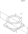
- Fig. 1 is an external perspective view of an indoor light source according to one embodiment of the present invention.
- Fig. 2 is a cross-sectional view of the indoor light source taken along a plane indicated by an imaginary line shown in Fig. 1 .
- the indoor light source 1 includes a substrate 2, a light-emitting device 3 located on the substrate 2, a frame 4 located on the substrate 2 to surround the light-emitting device 3, a sealant 5 filling an inner space defined by the frame 4 except an upper area of the inner space defined by the frame 4, and a wavelength conversion member 6 placed on the upper surface of the sealant 5 in the upper area of the inner space defined by the frame 4 to fit inside the frame 4.
- the light-emitting device 3 is, for example, a light-emitting diode (LED), and emits light when electrons and holes in the p-n junction in semiconductors are recombined.
- LED light-emitting diode
- the substrate 2 is an insulating substrate, and is formed from, for example, a ceramic material such as alumina and mullite, or a glass ceramic material. In some embodiments, the substrate 2 may be formed from a composite material containing two or more of these materials. The substrate 2 may contain a polymeric resin in which metallic oxide particles are dispersed to adjust the thermal expansion of the substrate 2.
- the substrate 2 has, on at least its main surface or its inside, a wiring conductor that provides electrical connection inside and outside the substrate 2.
- the wiring conductor is formed from, for example, a conductive material such as tungsten, molybdenum, manganese, or copper.
- the substrate 2 formed from a ceramic material may be prepared by, for example, applying a metal paste containing powder of, for example, tungsten containing an organic solvent in a predetermined pattern of a ceramic green sheet, which is to be the substrate 2, by printing, stacking a plurality of ceramic green sheets prepared in this manner on one another and firing the structure. This completes the substrate 2.
- the surface of the trace conductor is plated with, for example, nickel or gold, for preventing oxidation.
- the upper surface of the substrate 2 may be coated with a metallic reflective layer that is formed from, for example, aluminum, silver, gold, copper, or platina and is spaced from the wiring conductor and the plating layer to efficiently reflect light upward from the substrate 2.
- the light-emitting device 3 is mounted on the main surface of the substrate 2.
- the light-emitting device 3 is electrically connected on the plating layer on the surface of the wiring conductor on the main surface of the substrate 2 with, for example, brazing material or solder.
- the light-emitting device 3 includes a translucent base and an optical semiconductor layer formed on the translucent base.
- the translucent base allows an optical semiconductor layer to be deposited by chemical vapor deposition, such as metal organic chemical vapor deposition or molecular beam epitaxy.
- the translucent base may be formed from, for example, sapphire, gallium nitride, aluminum nitride, zinc oxide, zinc selenide, silicon carbide, silicon, or zirconium boride.
- the translucent base has a thickness of, for example, 50 to 1000 ⁇ m, inclusive.
- the optical semiconductor layer includes a first semiconductor layer formed on the translucent base, a light-emitting layer formed on the first semiconductor layer, and a second semiconductor layer formed on the light-emitting layer.
- the first semiconductor layer, the light-emitting layer, and the second semiconductor layer may be formed from, for example, a group III nitride semiconductor, a group III-V semiconductor, such as gallium phosphide and gallium arsenide, or a group III nitride semiconductor, such as gallium nitride, aluminum nitride, and indium nitride.
- the first semiconductor layer has a thickness of, for example, 1 to 5 ⁇ m inclusive.
- the light-emitting layer has a thickness of, for example, 25 to 150 nm inclusive.
- the second semiconductor layer has a thickness of, for example, 50 to 600 nm inclusive.
- the light-emitting device 3 formed in this manner may emit excitation light with a wavelength range of 370 to 420 nm
- the frame 4 is formed from a resin material that is a mixture of powders of, for example, a ceramic material such as aluminum oxide, titanium oxide, zirconium oxide, or yttrium oxide, a porous material, or a metallic oxide such as aluminum oxide, titanium oxide, zirconium oxide, or yttrium oxide.
- the frame 4 is bonded to the main surface of the substrate 2 with, for example, a resin.
- the frame 4 is spaced from and surrounds the light-emitting device 3.
- the frame 4 has an inner sloping wall that flares away from the main surface of the substrate 2.
- the inner wall of the frame 4 serves as a reflection surface for reflecting excitation light emitted from the light-emitting device 3. When the inner wall of the frame 4 is circular as viewed from above, the reflection surface can reflect light emitted from the light-emitting device 3 in all directions.
- the sloping inner wall of the frame 4 may have, for example, a metallic layer of tungsten, molybdenum, copper, or silver formed on the inner periphery of the frame 4 formed from a sintered material, and a plating metallic layer of nickel or gold covering the metallic layer.
- the plating metallic layer reflects light emitted from the light-emitting device 3.
- the inner wall of the frame 4 may have a slope angle of, for example, 55 to 70° inclusive with respect to the main surface of the substrate 2.
- the inner space of the frame 4 is filled with the sealant 5, which transmits light.
- the sealant 5, which seals the light-emitting device 3, can transmit light emitted from the light-emitting device 3.
- the sealant 5 fills the inner space of the frame 4 except an area of the inner space defined by the frame 4.
- the sealant 5 may be, for example, a translucent insulating resin, such as a silicone resin, an acrylic resin, and an epoxy resin.
- the sealant 5 has a refractive index of, for example, 1.4 to 1.6 inclusive.
- the wavelength conversion member 6 is placed on the upper surface of the sealant 5 in the upper area of the inner space defined by the frame 4.
- the wavelength conversion member 6 is sized to fit inside the frame 4.
- the wavelength conversion member 6 converts the wavelength of light emitted from the light-emitting device 3.
- the wavelength conversion member 6 receives light emitted from the light-emitting device 3.
- the light emitted from the light-emitting device 3 and incident on the wavelength conversion member 6 excites a phosphor material 7 in the wavelength conversion member 6, which then emits light.
- the wavelength conversion member 6 emits light by transmitting part of the light emitted from the light-emitting device 3 and the light emitted from the phosphor material 7.
- the wavelength conversion member 6 is formed from, for example, a translucent insulating resin, such as a fluororesin, a silicone resin, an acrylic resin, and an epoxy resin, or translucent glass.
- a translucent insulating resin such as a fluororesin, a silicone resin, an acrylic resin, and an epoxy resin, or translucent glass.
- the insulating resin or the glass contains the phosphor material 7.
- the phosphor material 7 is uniformly dispersed in the wavelength conversion member 6.
- the light-emitting device 3 and the phosphor material 7 used in the wavelength conversion member 6 are selected to obtain the indoor light source 1 that emits light with an emission spectrum S shown in Fig. 3 .
- the indoor light source 1 includes the light-emitting device 3 with a peak wavelength of 405 nm, and the phosphor material 7 including a red phosphor that shows a red fluorescence, a green phosphor that shows a green fluorescence, a first blue phosphor that shows a blue fluorescence with a first spectrum, and a second blue phosphor that shows a blue fluorescence with a second spectrum.
- the fluorescence spectrum of the first blue phosphor which is referred to as a first fluorescence spectrum
- the fluorescence spectrum of the second blue phosphor which is referred to as a second fluorescence spectrum
- a difference between the peak wavelength ⁇ B1 (nm) of the first fluorescence spectrum and the peak wavelength ⁇ B2 (nm) of the second fluorescence spectrum is 10 nm or less.
- the difference between the peak wavelength ⁇ B1 (nm) of the first fluorescence spectrum and the peak wavelength ⁇ B2 (nm) of the second fluorescence spectrum is 5 nm or less.
- the difference in the peak wavelength between the two blue phosphors is as small as 10 nm or less, and the peak wavelength ⁇ B1 (nm) of the first fluorescence spectrum and the peak wavelength ⁇ B2 (nm) of the second fluorescence spectrum differ from each other.
- the difference may be 0 nm, or in other words, the peak wavelength ⁇ B1 may be equal to the peak wavelength ⁇ B2.
- the first fluorescence spectrum of the first blue phosphor and the second fluorescence spectrum of the second blue phosphor may be easily distinguished when the light intensities of the first blue phosphor and the second blue phosphor are determined using the emission spectrum of the indoor light source 1. This allows easy control of the light intensities of the first fluorescence spectrum of the first blue phosphor and the second fluorescence spectrum of the second blue phosphor.
- a smaller difference in the peak wavelength can increase the light intensity of the blue region with the peak wavelength ⁇ B1 (nm) of the first fluorescence spectrum and the peak wavelength ⁇ B2 (nm) of the second fluorescence spectrum at its center.
- the half width of the first fluorescence spectrum which is the fluorescence spectrum of the first blue phosphor, may differ from the half width of the second fluorescence spectrum, which is the fluorescence spectrum of the second blue phosphor.
- the half width of the second fluorescence spectrum which is the fluorescence spectrum of the second blue phosphor, may differ from and be greater at longer wavelengths than the half width of the first fluorescence spectrum, which is the fluorescence spectrum of the first blue phosphor.
- the half width of the first fluorescence spectrum HWB1 (nm) and the half width of the second fluorescence spectrum HWB2 (nm) differ from each other by 10 to 100 nm inclusive.
- the half width of the first fluorescence spectrum HWB1 (nm) and the half width of the second fluorescence spectrum HWB2 (nm) differ from each other by 10 nm or more.
- the second fluorescence spectrum which is the fluorescence spectrum of the second blue phosphor, is greater at longer wavelengths than the first fluorescence spectrum, which is the fluorescence spectrum of the first blue phosphor.
- the indoor light source 1 has a smaller difference in the peak wavelengths between the first blue phosphor and the second blue phosphor to increase the light intensity of the blue region, which is easily absorbed into the green phosphor, and may also combine light emitted from the first blue phosphor and the second blue phosphor with light having a wavelength of 500 to 600 nm, which is not easily absorbed into the green phosphor.
- the indoor light source 1 can thus reduce the difference in the light intensity between the peak wavelengths in the blue region and the green region, and increase the light intensities of the wavelengths falling between the peak wavelength in the blue region and the peak wavelength in the green region. This allows emission of light with higher color rendering having a spectrum similar to the spectrum of sunlight.
- the indoor light source 1 has the emission spectrum in which ⁇ 1 (nm) is the peak wavelength at a first peak with the highest light intensity in the blue region, ⁇ 2 (nm) is the peak wavelength at a second peak in the green region, and ⁇ 3 (nm) is the peak wavelength at a third peak in the red region.
- the two different blue phosphors allow the light intensity at the wavelength ⁇ 1 (nm) to remain high, prevent the light intensity in the wavelength region from the wavelength ⁇ 1 to the wavelength ⁇ 2 (nm) from decreasing, and maintain the lowest light intensity of 0.7 or higher, or more specifically 0.85 or higher in terms of relative intensity in the wavelength region.
- the red phosphor is Y 2 O 2 S:Eu, Y 2 O 3 :Eu, SrCaClAlSiN 3 :Eu 2+ , CaAlSiN 3 :Eu, or CaAlSi(ON) 3 :Eu.
- the green phosphor is SrSi 2 (O, Cl) 2 N 2 :Eu, (Sr, Ba, Mg) 2 SiO 4 :Eu 2+ , ZnS:Cu, Al, or Zn 2 SiO 4 :Mn.
- the first blue phosphor is BaMgAl 10 O 17 :Eu or (Sr, Ba) 10 (PO 4 ) 6 Cl 2 :Eu.
- the second blue phosphor is (Sr, Ba, Ca) 5 (PO 4 ) 3 Cl:Eu.
- the indoor light source 1 used as an illumination apparatus for indoor use intends its emission spectrum that satisfies the characteristics described below.
- the emission spectrum includes a first peak with the highest light intensity in a wavelength region of 440 to 460 nm, a second peak in a wavelength region of 540 to 560 nm, and a third peak in a wavelength region of 610 to 630 nm, ⁇ 1 (nm) is the peak wavelength at the first peak, ⁇ 2 (nm) is the peak wavelength at the second peak, and ⁇ 3 (nm) is the peak wavelength at the third peak.
- the highest one of the intensities at the first to third peaks is 1 in terms of relative intensity.
- the emission spectrum includes the lowest light intensity of 0.7 or higher in terms of relative intensity in the wavelength region of ⁇ 1 to ⁇ 2 (nm), and the lowest light intensity of 0.8 or higher in terms of relative intensity in the wavelength region of ⁇ 2 to ⁇ 3 (nm).
- the emission spectrum has no limitation in the regions of wavelengths lower than ⁇ 1 (nm) and higher than ⁇ 3 (nm)
- light with a wavelength of 380 nm or lower or 780 nm or higher in the ultraviolet region or in the infrared region is difficult to recognize as visible light, and thus is to be reduced in these regions.
- the emission spectrum of the light emitted from the indoor light source 1 according to the present embodiment constantly has the light intensity of 0.7 or higher in terms of relative intensity in the wavelength region of ⁇ 1 to ⁇ 3 (nm), and the spectrum is more similar to the spectrum of sunlight than the emission spectrum of the light emitted from known light sources.
- the indoor light source 1 according to the present embodiment can emit light with higher color rendering, in addition to having a smaller difference between the highest and the lowest values of the light intensity in the wavelength region of ⁇ 1 to ⁇ 3 (nm).
- the emission spectrum according to the present embodiment may include the lowest light intensity of 0.85 or higher in terms of relative intensity in the wavelength region of ⁇ 1 to ⁇ 2 (nm), and may include the lowest light intensity of 0.95 or higher in the wavelength region of ⁇ 2 to ⁇ 3 (nm) in terms of relative intensity.
- This emission spectrum constantly includes the light intensity of 0.85 or higher in terms of relative intensity in the wavelength region of ⁇ 1 to ⁇ 3 (nm).
- the indoor light source 1 according to the present embodiment can thus emit light with higher color rendering, enabling the spectrum to be more similar to the spectrum of sunlight.
- this structure reduces the difference between the relative intensities in the spectrum of sunlight and in the emission spectrum of the indoor light source 1 according to the present embodiment.
- the resultant indoor light source 1 can produce light similar to sunlight.
- the emission spectrum according to the present embodiment has two of the light intensities at the first to third peaks except the highest light intensity that may be both 0.99 or higher in terms of relative intensity.
- the emission spectrum according to the present invention has two of the light intensities at the first to third peaks except the highest light intensity that are both 0.99 or higher in terms of relative intensity.
- This emission spectrum has the three peak wavelengths having almost the same light intensity. This reduces the difference in the relative intensity between the spectrum of sunlight and the emission spectrum according to the present embodiment.
- the indoor light source 1 according to the present embodiment can thus emit light with higher color rendering, with the spectrum more similar to the spectrum of sunlight.
- the emission spectrum according to the present invention includes the light intensity of 0.6 or higher in terms of relative intensity at 405 nm.
- the emission spectrum according to the present embodiment includes the light intensity of 0.6 or higher in terms of relative intensity at 405 nm, and the light intensity of 0.4 or lower in terms of relative intensity at 400 nm.
- the emission spectrum may further include the light intensity of 0.8 or higher in terms of relative intensity at 650 nm, and the light intensity of 0.35 or higher in terms of relative intensity at 700 nm.
- the indoor light source 1 can thus efficiently emit light with higher color rendering, being more similar to sunlight and having reduced energy of light that is difficult to recognize as visible light.
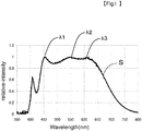
- Fig. 3 shows an example of the emission spectrum S of light emitted from the indoor light source 1 according to the present embodiment.
- the emission spectrum S shown in Fig. 3 is based on actual values measured in the example described below.
- the emission spectrum S shown in Fig. 3 includes the peak wavelength of 452 nm at the first peak ⁇ 1 (nm), and the light intensity of 0.997 in terms of relative intensity at the peak ⁇ 1 (nm).
- the peak wavelength at the second peak ⁇ 2 (nm) is 553 nm, and the light intensity at ⁇ 2 (nm) is 1 in terms of relative intensity.
- the peak wavelength at the third peak ⁇ 3 (nm) is 616 nm, and the light intensity at ⁇ 3 (nm) is 0.994 in terms of relative intensity.
- the lowest light intensity in the wavelength region of ⁇ 1 to ⁇ 2 (nm) is 0.877 in terms of relative intensity.
- the lowest light intensity in the wavelength region of ⁇ 2 to ⁇ 3 (nm) is 0.953 in terms of relative intensity.
- the light intensity at 650 nm is 0.842 in terms of relative intensity, and the light intensity at 700 nm is 0.399 in terms of relative intensity.
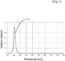
- Fig. 4 shows an example of an emission spectrum L of excitation light emitted from the light-emitting device 3 included in the indoor light source 1 according to the present embodiment.
- Fig. 5 shows examples of a fluorescence spectrum R of a red phosphor, a fluorescence spectrum G of a green phosphor, a first fluorescence spectrum B1 of a first blue phosphor, and a second fluorescence spectrum B2 of a second blue phosphor included in the phosphor material 7 used in the indoor light source 1 according to the present embodiment.
- These spectra are shown in terms of relative intensity based on the highest light intensity of each spectrum expressed as 1.
- the emission spectrum L shown in Fig. 4 and the fluorescence spectra B1, B2, G, and R shown in Fig. 5 are based on actual values measured in the example described later.
- the fluorescence spectra B1, B2, G, and R shown in Fig. 5 include the peak wavelength ⁇ B1 of 450 nm in the first fluorescence spectrum B1.
- the peak wavelength ⁇ B2 of the second fluorescence spectrum B2 is 453 nm.
- the difference between the wavelengths ⁇ B1 and ⁇ B2 is 3 nm.
- the half width HWB1 of the first fluorescence spectrum B1 is 39 nm.
- the half width HWB2 of the second fluorescence spectrum B2 is 52 nm.
- the difference between the half widths HWB1 and HWB2 is 13 nm.
- the indoor light source 1 is used in an illumination apparatus for indoor use, such as in a building or in a house.
- a plurality of indoor light sources 1 are arranged.
- an illumination apparatus for a living space including the indoor light source(s) 1 placed indoors can create a lighting environment that simulates an environment illuminated with sunlight.
- an illumination apparatus for visual inspection of painted products, such as automobiles, including the indoor light source(s) 1 placed indoors can create an inspection environment simulating an environment illuminated with sunlight.
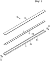
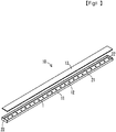
- Fig. 6 is an external perspective view of an illumination apparatus including the indoor light source according to the present embodiment.
- Fig. 7 is an exploded perspective view of the illumination apparatus shown in Fig. 6 .
- Fig. 8 is a perspective view of the illumination apparatus shown in Fig. 6 with a translucent substrate removed from a housing.
- the illumination apparatus 10 includes a housing 11, indoor light sources 1, a wiring board 12, and a translucent substrate 13.
- the housing 11 is elongated and is open upward.
- the multiple indoor light sources 1 are arranged in line in the longitudinal direction in the housing 11.
- the wiring board 12 is elongated, and includes the multiple indoor light sources 1 mounted on it.
- the translucent substrate 13 is elongated, and is supported by the housing 11 and seals the opening of the housing 11.
- the housing 11 supports the translucent substrate 13 and dissipates heat generated by the indoor light sources 1 outside.
- the housing 11 is formed from, for example, metal, such as aluminum, copper, or stainless steel, or plastics, or a resin.
- the housing 11 has a bottom 21a extending in the longitudinal direction, a pair of supports 21b extending upright from the two ends of the bottom 21a in the width direction and extending in the longitudinal direction, an elongated body 21 that is open upward and open at two ends in the longitudinal direction, and two lids 22 for sealing the open ends in the longitudinal direction of the body 21.
- the supports 21b each have top holders including recesses facing each other to support the translucent substrate 13.
- the housing 11 has a length of, for example, 100 to 2000 mm inclusive, in the longitudinal direction.
- the wiring board 12 is fixed on the bottom inside the housing 11.
- the wiring board 12 may be, for example, a printed board such as a rigid printed board, a flexible printed board, or a rigid flexible printed board.
- the wiring pattern on the wiring board 12 and the wiring pattern on the substrate 2 included in each indoor light source 1 are electrically connected to each other with solder or conductive adhesive.
- a signal from the wiring board 12 is transmitted to the light-emitting device 3 through the substrate 2.
- the light-emitting device 3 then emits light.
- the wiring board 12 may be powered by an external power source through wiring.
- the translucent substrate 13 is formed from a material that transmits light emitted from each indoor light source 1.
- the translucent substrate 13 may be formed from, for example, a translucent material such as an acrylic resin or glass.
- the translucent substrate 13 is a rectangular plate, and has a length of, for example, 98 to 1998 mm inclusive in the longitudinal direction.
- the translucent substrate 13 is inserted through either of the two open end of the main body 21 in the longitudinal direction along the recesses on the holders.
- the translucent substrate 13 is then slid in the longitudinal direction, and thus is supported by the pair of supports 21b at positions spaced from the multiple indoor light sources 1.
- the open ends of the main body 21 in the longitudinal direction are then covered with the lids 22. This completes the illumination apparatus 10.
- the illumination apparatus 10 described above is a linear light emitting apparatus including the multiple indoor light sources 1 arranged in line.
- the illumination apparatus 10 may be a surface light emitting apparatus including multiple indoor light sources 1 arranged in a matrix or in a staggered pattern.
- each indoor light source 1 may include two different wavelength conversion members.
- a first wavelength conversion member may include a red phosphor, a green phosphor, and a first blue phosphor
- a second wavelength conversion member may include a red phosphor, a green phosphor, and a second blue phosphor.
- These two different wavelength conversion members may be included in each indoor light source to combine light emitted through each wavelength conversion member. More specifically, the wavelength conversion member 6 including the first wavelength conversion member and the second wavelength conversion member stacked on each other is placed on the upper surface of the sealant 5 in an upper area of the inner space defined by the frame 4.
- the wavelength conversion member 6 may include multiple first wavelength conversion members and multiple second wavelength conversion members stacked on one another.
- the illumination apparatus may further include two different indoor light sources.
- a first indoor light source includes the above first wavelength conversion member
- a second indoor light source includes the above second wavelength conversion member.
- the illumination apparatus may emit light obtained by combining light emitted from the first indoor light source and light emitted from the second indoor light source.
- the indoor light source 1 shown in Figs. 1 and 2 was fabricated, and evaluated for its color rendering.
- the light-emitting device 3, which emits excitation light, is a gallium nitride light-emitting device that emits light with a peak wavelength of 405 nm and a half width of 15 nm, and has the emission spectrum L shown in Fig. 4 .
- the red phosphor is CaAlSi(ON) 3 :Eu, and has the fluorescence spectrum R shown in Fig. 5 .
- the green phosphor is SrSi 2 (O, Cl) 2 N 2 :Eu, and has the fluorescence spectrum G shown in Fig. 5 .
- the first blue phosphor is (Sr, Ba) 10 (PO 4 )6Cl 2 :Eu, and has the fluorescence spectrum B1 shown in Fig. 5 .
- the second blue phosphor is (Sr, Ba, Ca) 5 (PO 4 ) 3 Cl:Eu, and has the fluorescence spectrum B2 shown in Fig. 5 .
- the resultant indoor light source 1 has the emission spectrum S shown in Fig. 3 .
- the indoor light source 1 then evaluated for its color rendering with the method for evaluating color rendering of light sources defined by JIS Z8726-1990.
- the indoor light source 1 in the present example is used as a test light source
- the chromaticity coordinates (x, y) are set to the coordinates (0.3443, 0.3558)
- CIE daylight is used as a reference illuminant.
- Table 1 shows the measurement results of color rendering using the general color rendering index Ra and the special color rendering indexes R1 to R15 for each test color sample.
- the general color rendering index Ra (arithmetic average of R1 to R8) tends to be higher as the light is more similar to sunlight (with the highest value of 100). Thus, when the emission spectrum of the indoor light source 1 as the test light source is more similar to the spectrum of sunlight, the index Ra is higher, indicating that the color rendering is higher.
- the general color rendering index Ra of the indoor light source 1 as the test light source is as high as 97.3 as shown in Table 1, whereas the other special color rendering indexes R1 to R15 are also high.
- the indoor light source 1 emits light with the emission spectrum shown in Fig. 3 that is similar to the emission spectrum of sunlight.
- the resultant indoor light source 1 achieves high color rendering.
Landscapes
- Engineering & Computer Science (AREA)
- Microelectronics & Electronic Packaging (AREA)
- General Engineering & Computer Science (AREA)
- Manufacturing & Machinery (AREA)
- Computer Hardware Design (AREA)
- Power Engineering (AREA)
- Physics & Mathematics (AREA)
- Spectroscopy & Molecular Physics (AREA)
- Optics & Photonics (AREA)
- Led Device Packages (AREA)
- Non-Portable Lighting Devices Or Systems Thereof (AREA)
Claims (4)
- Innenraum-Lichtquelle (1), die Licht mit einem Emissionsspektrum emittiert, das einen ersten Peak in einem Wellenlängenbereich von 440 bis 460 nm, einen zweiten Peak in einem Wellenlängenbereich von 540 bis 560 nm und einen dritten Peak in einem Wellenlängenbereich von 610 bis 630 nm hat,
wobei, wenn die höchste der Intensitäten beim ersten Peak, beim zweiten Peak und beim dritten Peak bezogen auf die relative Intensität 1 ist, das Emissionsspektrum eine niedrigste Lichtintensität von 0,7 oder höher bezogen auf die relative Intensität in einem Wellenlängenbereich von λ1 bis A2 in nm und eine niedrigste Lichtintensität von 0,8 oder höher bezogen auf die relative Intensität in einem Wellenlängenbereich von A2 bis A3 in nm aufweist, und
wobei λ1 eine Peak-Wellenlänge beim ersten Peak in nm ist, λ2 eine Peak-Wellenlänge beim zweiten Peak in nm ist und A3 eine Peak-Wellenlänge beim dritten Peak in nm ist,
wobei die Innenraum-Lichtquelle (1) eine lichtemittierende Vorrichtung (3) aufweist, die konfiguriert ist, um ultraviolettes Licht (6) zu emittieren,
wobei ein Wellenlängenumwandlungselement (6) ein anorganisches Material aufweist, das einen darin dispergierten Leuchtstoff (7) enthält, wobei der Leuchtstoff (7) durch von der lichtemittierenden Vorrichtung (3) emittiertes Licht anzuregen ist, um eine Fluoreszenz zu zeigen, wobei der Leuchtstoff (7) einen roten Leuchtstoff, der eine rote Fluoreszenz zeigt, einen grünen Leuchtstoff, der eine grüne Fluoreszenz zeigt, einen ersten blauen Leuchtstoff, der eine blaue Fluoreszenz mit einem ersten Fluoreszenzspektrum zeigt, und einen zweiten blauen Leuchtstoff, der eine blaue Fluoreszenz mit einem zweiten Fluoreszenzspektrum zeigt, aufweist,
dadurch gekennzeichnet, dass
das Emissionsspektrum zwei Lichtintensitäten von 0,99 oder höher bezogen auf die relative Intensität beim ersten bis dritten Peak aufweist, ausschließlich eines Peaks mit der höchsten Lichtintensität vom ersten bis dritten Peak, und die Lichtintensität von 0,6 oder höher bezogen auf die relative Intensität bei 405 nm aufweist,
eine Differenz zwischen einer Peak-Wellenlänge λB1 in nm des ersten Fluoreszenzspektrums und einer Peak-Wellenlänge AB2 in nm des zweiten Fluoreszenzspektrums 5 nm oder weniger beträgt, und
eine Differenz zwischen einer Halbwertsbreite HWB1 in nm des ersten Fluoreszenzspektrums und einer Halbwertsbreite HWB2 in nm des zweiten Fluoreszenzspektrums 10 nm oder mehr beträgt. - Innenraum-Lichtquelle (1) gemäß Anspruch 1, wobei
das Emissionsspektrum eine Lichtintensität von 0,8 oder höher bezogen auf die relative Intensität bei 650 nm und eine Lichtintensität von 0,35 oder höher bezogen auf die relative Intensität bei 700 nm aufweist. - Innenraum-Lichtquelle (1) gemäß Anspruch 1 oder Anspruch 2, wobei
das Emissionsspektrum eine niedrigste Lichtintensität von 0,85 oder höher bezogen auf die relative Intensität in einem Wellenlängenbereich von λ1 bis λ2 in nm, und eine niedrigste Lichtintensität von 0,95 oder höher bezogen auf die relative Intensität in einem Wellenlängenbereich von λ2 bis A3 in nm aufweist. - Beleuchtungsvorrichtung (10), aufweisend:
eine Mehrzahl der Innenlichtquellen (1) gemäß irgendeinem der Ansprüche 1 bis 3.
Applications Claiming Priority (2)
| Application Number | Priority Date | Filing Date | Title |
|---|---|---|---|
| JP2015206120 | 2015-10-20 | ||
| PCT/JP2016/081134 WO2017069206A1 (ja) | 2015-10-20 | 2016-10-20 | 屋内用光源および照明装置 |
Publications (3)
| Publication Number | Publication Date |
|---|---|
| EP3367448A1 EP3367448A1 (de) | 2018-08-29 |
| EP3367448A4 EP3367448A4 (de) | 2019-05-29 |
| EP3367448B1 true EP3367448B1 (de) | 2021-04-28 |
Family
ID=58557192
Family Applications (1)
| Application Number | Title | Priority Date | Filing Date |
|---|---|---|---|
| EP16857519.9A Active EP3367448B1 (de) | 2015-10-20 | 2016-10-20 | Innenraumlichtquelle und beleuchtungsvorrichtung |
Country Status (4)
| Country | Link |
|---|---|
| US (1) | US10337697B2 (de) |
| EP (1) | EP3367448B1 (de) |
| JP (2) | JP6698676B2 (de) |
| WO (1) | WO2017069206A1 (de) |
Families Citing this family (11)
| Publication number | Priority date | Publication date | Assignee | Title |
|---|---|---|---|---|
| KR101995000B1 (ko) * | 2016-05-16 | 2019-07-01 | 엘지이노텍 주식회사 | 발광소자 패키지 및 조명장치 |
| JP7025424B2 (ja) * | 2017-06-28 | 2022-02-24 | 京セラ株式会社 | 発光装置および照明装置 |
| KR102154552B1 (ko) * | 2017-09-28 | 2020-09-11 | 루미리즈 홀딩 비.브이. | 적외선 방출 디바이스 |
| WO2019106864A1 (ja) * | 2017-11-28 | 2019-06-06 | 京セラ株式会社 | 発光装置および照明装置 |
| JPWO2019107281A1 (ja) * | 2017-11-28 | 2020-12-03 | 京セラ株式会社 | 発光装置および照明装置 |
| CN112106443A (zh) * | 2018-01-11 | 2020-12-18 | 生态照明公司 | 用于提供可调光和功能性二极管发射的多通道系统 |
| WO2019146327A1 (ja) * | 2018-01-29 | 2019-08-01 | 京セラ株式会社 | 発光装置および照明装置 |
| JPWO2019164014A1 (ja) * | 2018-02-26 | 2021-02-04 | 京セラ株式会社 | 発光装置および照明装置 |
| EP3890447A4 (de) * | 2018-11-27 | 2022-08-10 | Kyocera Corporation | Beleuchtungsvorrichtung |
| US20220268423A1 (en) * | 2019-08-07 | 2022-08-25 | Kyocera Corporation | Lighting device |
| JP7233559B2 (ja) * | 2019-10-18 | 2023-03-06 | 京セラ株式会社 | 発光装置及び照明装置 |
Family Cites Families (12)
| Publication number | Priority date | Publication date | Assignee | Title |
|---|---|---|---|---|
| US6621211B1 (en) * | 2000-05-15 | 2003-09-16 | General Electric Company | White light emitting phosphor blends for LED devices |
| JP2002190622A (ja) * | 2000-12-22 | 2002-07-05 | Sanken Electric Co Ltd | 発光ダイオード用透光性蛍光カバー |
| US7753553B2 (en) * | 2005-06-02 | 2010-07-13 | Koniklijke Philips Electronics N.V. | Illumination system comprising color deficiency compensating luminescent material |
| KR100682876B1 (ko) * | 2005-07-06 | 2007-02-15 | 삼성전기주식회사 | 실리코포스페이트계 형광체 및 이를 포함한 led |
| JP2011029497A (ja) * | 2009-07-28 | 2011-02-10 | Mitsubishi Chemicals Corp | 白色発光装置およびそれを用いた照明装置 |
| JP5370047B2 (ja) * | 2009-09-25 | 2013-12-18 | 三菱化学株式会社 | 白色発光装置のための演色性改善方法および白色発光装置 |
| KR101144754B1 (ko) * | 2010-01-19 | 2012-05-09 | 일진반도체 주식회사 | 백색 발광장치 및 이의 제조방법 |
| JP5105132B1 (ja) * | 2011-06-02 | 2012-12-19 | 三菱化学株式会社 | 半導体発光装置、半導体発光システムおよび照明器具 |
| US9082939B2 (en) | 2011-10-24 | 2015-07-14 | Kabushiki Kaisha Toshiba | White light source and white light source system including the same |
| EP3483496B1 (de) * | 2011-11-07 | 2020-07-29 | Kabushiki Kaisha Toshiba | Weisslichtquelle und weisslichtquellensystem damit |
| CN104718633B (zh) * | 2012-10-04 | 2017-09-26 | 株式会社东芝 | 白色发光装置、照明装置、以及牙科用照明装置 |
| JP2015126160A (ja) * | 2013-12-27 | 2015-07-06 | サンケン電気株式会社 | 発光装置 |
-
2016
- 2016-10-20 US US15/764,135 patent/US10337697B2/en active Active
- 2016-10-20 JP JP2017545789A patent/JP6698676B2/ja active Active
- 2016-10-20 EP EP16857519.9A patent/EP3367448B1/de active Active
- 2016-10-20 WO PCT/JP2016/081134 patent/WO2017069206A1/ja active Application Filing
-
2020
- 2020-04-27 JP JP2020078377A patent/JP6913790B2/ja active Active
Non-Patent Citations (1)
| Title |
|---|
| None * |
Also Published As
| Publication number | Publication date |
|---|---|
| US10337697B2 (en) | 2019-07-02 |
| JP2020129684A (ja) | 2020-08-27 |
| EP3367448A4 (de) | 2019-05-29 |
| EP3367448A1 (de) | 2018-08-29 |
| WO2017069206A1 (ja) | 2017-04-27 |
| JP6913790B2 (ja) | 2021-08-04 |
| JP6698676B2 (ja) | 2020-05-27 |
| US20180274754A1 (en) | 2018-09-27 |
| JPWO2017069206A1 (ja) | 2018-08-16 |
Similar Documents
| Publication | Publication Date | Title |
|---|---|---|
| EP3367448B1 (de) | Innenraumlichtquelle und beleuchtungsvorrichtung | |
| US10854792B2 (en) | Light-emitting device and illumination apparatus | |
| EP3008374B1 (de) | Lichtemittierende anordnung mit angepasster ausgangsspektrums | |
| JP6363061B2 (ja) | 白色発光モジュール | |
| EP3690963B1 (de) | Lichtemittierende vorrichtung und beleuchtungsvorrichtung | |
| JP2010267571A (ja) | 照明装置 | |
| JP2022103159A (ja) | 発光装置、照明装置および生物育成用の照明装置 | |
| JP5658462B2 (ja) | 照明装置 | |
| JP2014112621A (ja) | 半導体発光装置及び照明装置 | |
| US11495716B2 (en) | Light-emitting device and illumination apparatus | |
| WO2019107281A1 (ja) | 発光装置および照明装置 | |
| JP7027161B2 (ja) | 照明装置および照明モジュール | |
| JP2017117853A (ja) | 発光装置、及び、照明装置 | |
| JP3243360U (ja) | 生物育成用の照明装置 | |
| JP7274013B2 (ja) | 照明装置および照明モジュール | |
| JP7042683B2 (ja) | 照明装置 | |
| JP2020107422A (ja) | 照明装置および照明システム |
Legal Events
| Date | Code | Title | Description |
|---|---|---|---|
| STAA | Information on the status of an ep patent application or granted ep patent |
Free format text: STATUS: THE INTERNATIONAL PUBLICATION HAS BEEN MADE |
|
| PUAI | Public reference made under article 153(3) epc to a published international application that has entered the european phase |
Free format text: ORIGINAL CODE: 0009012 |
|
| STAA | Information on the status of an ep patent application or granted ep patent |
Free format text: STATUS: REQUEST FOR EXAMINATION WAS MADE |
|
| 17P | Request for examination filed |
Effective date: 20180319 |
|
| AK | Designated contracting states |
Kind code of ref document: A1 Designated state(s): AL AT BE BG CH CY CZ DE DK EE ES FI FR GB GR HR HU IE IS IT LI LT LU LV MC MK MT NL NO PL PT RO RS SE SI SK SM TR |
|
| AX | Request for extension of the european patent |
Extension state: BA ME |
|
| DAV | Request for validation of the european patent (deleted) | ||
| DAX | Request for extension of the european patent (deleted) | ||
| RIC1 | Information provided on ipc code assigned before grant |
Ipc: H01L 33/00 20100101ALI20170510BHEP Ipc: F21V 9/16 20060101ALI20170510BHEP Ipc: F21S 2/00 20160101ALI20170510BHEP Ipc: H01L 33/50 20100101AFI20170510BHEP Ipc: F21Y 115/10 20160101ALI20170510BHEP |
|
| A4 | Supplementary search report drawn up and despatched |
Effective date: 20190429 |
|
| RIC1 | Information provided on ipc code assigned before grant |
Ipc: F21Y 115/10 20160101ALI20190423BHEP Ipc: F21S 4/20 20160101ALN20190423BHEP Ipc: H01L 33/00 20100101ALI20190423BHEP Ipc: H01L 33/50 20100101AFI20190423BHEP Ipc: F21V 9/30 20180101ALN20190423BHEP Ipc: F21S 2/00 20160101ALI20190423BHEP |
|
| STAA | Information on the status of an ep patent application or granted ep patent |
Free format text: STATUS: EXAMINATION IS IN PROGRESS |
|
| RIC1 | Information provided on ipc code assigned before grant |
Ipc: H01L 33/50 20100101AFI20200219BHEP Ipc: H01L 33/00 20100101ALI20200219BHEP Ipc: F21S 4/20 20160101ALN20200219BHEP Ipc: F21S 2/00 20160101ALI20200219BHEP Ipc: F21Y 115/10 20160101ALI20200219BHEP Ipc: F21V 9/30 20180101ALN20200219BHEP |
|
| 17Q | First examination report despatched |
Effective date: 20200312 |
|
| GRAP | Despatch of communication of intention to grant a patent |
Free format text: ORIGINAL CODE: EPIDOSNIGR1 |
|
| STAA | Information on the status of an ep patent application or granted ep patent |
Free format text: STATUS: GRANT OF PATENT IS INTENDED |
|
| RIC1 | Information provided on ipc code assigned before grant |
Ipc: H01L 33/00 20100101ALI20201022BHEP Ipc: F21S 2/00 20160101ALI20201022BHEP Ipc: F21S 4/20 20160101ALN20201022BHEP Ipc: H01L 33/50 20100101AFI20201022BHEP Ipc: F21V 9/30 20180101ALN20201022BHEP Ipc: F21Y 115/10 20160101ALI20201022BHEP |
|
| RIC1 | Information provided on ipc code assigned before grant |
Ipc: H01L 33/50 20100101AFI20201027BHEP Ipc: H01L 33/00 20100101ALI20201027BHEP Ipc: F21S 2/00 20160101ALI20201027BHEP Ipc: F21Y 115/10 20160101ALI20201027BHEP Ipc: F21V 9/30 20180101ALN20201027BHEP Ipc: F21S 4/20 20160101ALN20201027BHEP |
|
| INTG | Intention to grant announced |
Effective date: 20201124 |
|
| GRAS | Grant fee paid |
Free format text: ORIGINAL CODE: EPIDOSNIGR3 |
|
| GRAA | (expected) grant |
Free format text: ORIGINAL CODE: 0009210 |
|
| STAA | Information on the status of an ep patent application or granted ep patent |
Free format text: STATUS: THE PATENT HAS BEEN GRANTED |
|
| AK | Designated contracting states |
Kind code of ref document: B1 Designated state(s): AL AT BE BG CH CY CZ DE DK EE ES FI FR GB GR HR HU IE IS IT LI LT LU LV MC MK MT NL NO PL PT RO RS SE SI SK SM TR |
|
| REG | Reference to a national code |
Ref country code: GB Ref legal event code: FG4D |
|
| REG | Reference to a national code |
Ref country code: CH Ref legal event code: EP |
|
| REG | Reference to a national code |
Ref country code: AT Ref legal event code: REF Ref document number: 1388097 Country of ref document: AT Kind code of ref document: T Effective date: 20210515 |
|
| REG | Reference to a national code |
Ref country code: DE Ref legal event code: R096 Ref document number: 602016057093 Country of ref document: DE |
|
| REG | Reference to a national code |
Ref country code: IE Ref legal event code: FG4D |
|
| REG | Reference to a national code |
Ref country code: LT Ref legal event code: MG9D |
|
| REG | Reference to a national code |
Ref country code: AT Ref legal event code: MK05 Ref document number: 1388097 Country of ref document: AT Kind code of ref document: T Effective date: 20210428 |
|
| PG25 | Lapsed in a contracting state [announced via postgrant information from national office to epo] |
Ref country code: FI Free format text: LAPSE BECAUSE OF FAILURE TO SUBMIT A TRANSLATION OF THE DESCRIPTION OR TO PAY THE FEE WITHIN THE PRESCRIBED TIME-LIMIT Effective date: 20210428 Ref country code: LT Free format text: LAPSE BECAUSE OF FAILURE TO SUBMIT A TRANSLATION OF THE DESCRIPTION OR TO PAY THE FEE WITHIN THE PRESCRIBED TIME-LIMIT Effective date: 20210428 Ref country code: NL Free format text: LAPSE BECAUSE OF FAILURE TO SUBMIT A TRANSLATION OF THE DESCRIPTION OR TO PAY THE FEE WITHIN THE PRESCRIBED TIME-LIMIT Effective date: 20210428 Ref country code: HR Free format text: LAPSE BECAUSE OF FAILURE TO SUBMIT A TRANSLATION OF THE DESCRIPTION OR TO PAY THE FEE WITHIN THE PRESCRIBED TIME-LIMIT Effective date: 20210428 Ref country code: AT Free format text: LAPSE BECAUSE OF FAILURE TO SUBMIT A TRANSLATION OF THE DESCRIPTION OR TO PAY THE FEE WITHIN THE PRESCRIBED TIME-LIMIT Effective date: 20210428 Ref country code: BG Free format text: LAPSE BECAUSE OF FAILURE TO SUBMIT A TRANSLATION OF THE DESCRIPTION OR TO PAY THE FEE WITHIN THE PRESCRIBED TIME-LIMIT Effective date: 20210728 |
|
| PG25 | Lapsed in a contracting state [announced via postgrant information from national office to epo] |
Ref country code: IS Free format text: LAPSE BECAUSE OF FAILURE TO SUBMIT A TRANSLATION OF THE DESCRIPTION OR TO PAY THE FEE WITHIN THE PRESCRIBED TIME-LIMIT Effective date: 20210828 Ref country code: GR Free format text: LAPSE BECAUSE OF FAILURE TO SUBMIT A TRANSLATION OF THE DESCRIPTION OR TO PAY THE FEE WITHIN THE PRESCRIBED TIME-LIMIT Effective date: 20210729 Ref country code: LV Free format text: LAPSE BECAUSE OF FAILURE TO SUBMIT A TRANSLATION OF THE DESCRIPTION OR TO PAY THE FEE WITHIN THE PRESCRIBED TIME-LIMIT Effective date: 20210428 Ref country code: PT Free format text: LAPSE BECAUSE OF FAILURE TO SUBMIT A TRANSLATION OF THE DESCRIPTION OR TO PAY THE FEE WITHIN THE PRESCRIBED TIME-LIMIT Effective date: 20210830 Ref country code: PL Free format text: LAPSE BECAUSE OF FAILURE TO SUBMIT A TRANSLATION OF THE DESCRIPTION OR TO PAY THE FEE WITHIN THE PRESCRIBED TIME-LIMIT Effective date: 20210428 Ref country code: NO Free format text: LAPSE BECAUSE OF FAILURE TO SUBMIT A TRANSLATION OF THE DESCRIPTION OR TO PAY THE FEE WITHIN THE PRESCRIBED TIME-LIMIT Effective date: 20210728 Ref country code: SE Free format text: LAPSE BECAUSE OF FAILURE TO SUBMIT A TRANSLATION OF THE DESCRIPTION OR TO PAY THE FEE WITHIN THE PRESCRIBED TIME-LIMIT Effective date: 20210428 Ref country code: RS Free format text: LAPSE BECAUSE OF FAILURE TO SUBMIT A TRANSLATION OF THE DESCRIPTION OR TO PAY THE FEE WITHIN THE PRESCRIBED TIME-LIMIT Effective date: 20210428 |
|
| REG | Reference to a national code |
Ref country code: NL Ref legal event code: MP Effective date: 20210428 |
|
| PG25 | Lapsed in a contracting state [announced via postgrant information from national office to epo] |
Ref country code: DK Free format text: LAPSE BECAUSE OF FAILURE TO SUBMIT A TRANSLATION OF THE DESCRIPTION OR TO PAY THE FEE WITHIN THE PRESCRIBED TIME-LIMIT Effective date: 20210428 Ref country code: CZ Free format text: LAPSE BECAUSE OF FAILURE TO SUBMIT A TRANSLATION OF THE DESCRIPTION OR TO PAY THE FEE WITHIN THE PRESCRIBED TIME-LIMIT Effective date: 20210428 Ref country code: EE Free format text: LAPSE BECAUSE OF FAILURE TO SUBMIT A TRANSLATION OF THE DESCRIPTION OR TO PAY THE FEE WITHIN THE PRESCRIBED TIME-LIMIT Effective date: 20210428 Ref country code: ES Free format text: LAPSE BECAUSE OF FAILURE TO SUBMIT A TRANSLATION OF THE DESCRIPTION OR TO PAY THE FEE WITHIN THE PRESCRIBED TIME-LIMIT Effective date: 20210428 Ref country code: RO Free format text: LAPSE BECAUSE OF FAILURE TO SUBMIT A TRANSLATION OF THE DESCRIPTION OR TO PAY THE FEE WITHIN THE PRESCRIBED TIME-LIMIT Effective date: 20210428 Ref country code: SK Free format text: LAPSE BECAUSE OF FAILURE TO SUBMIT A TRANSLATION OF THE DESCRIPTION OR TO PAY THE FEE WITHIN THE PRESCRIBED TIME-LIMIT Effective date: 20210428 Ref country code: SM Free format text: LAPSE BECAUSE OF FAILURE TO SUBMIT A TRANSLATION OF THE DESCRIPTION OR TO PAY THE FEE WITHIN THE PRESCRIBED TIME-LIMIT Effective date: 20210428 |
|
| REG | Reference to a national code |
Ref country code: DE Ref legal event code: R097 Ref document number: 602016057093 Country of ref document: DE |
|
| PLBE | No opposition filed within time limit |
Free format text: ORIGINAL CODE: 0009261 |
|
| STAA | Information on the status of an ep patent application or granted ep patent |
Free format text: STATUS: NO OPPOSITION FILED WITHIN TIME LIMIT |
|
| 26N | No opposition filed |
Effective date: 20220131 |
|
| REG | Reference to a national code |
Ref country code: CH Ref legal event code: PL |
|
| PG25 | Lapsed in a contracting state [announced via postgrant information from national office to epo] |
Ref country code: IS Free format text: LAPSE BECAUSE OF FAILURE TO SUBMIT A TRANSLATION OF THE DESCRIPTION OR TO PAY THE FEE WITHIN THE PRESCRIBED TIME-LIMIT Effective date: 20210828 Ref country code: AL Free format text: LAPSE BECAUSE OF FAILURE TO SUBMIT A TRANSLATION OF THE DESCRIPTION OR TO PAY THE FEE WITHIN THE PRESCRIBED TIME-LIMIT Effective date: 20210428 |
|
| REG | Reference to a national code |
Ref country code: BE Ref legal event code: MM Effective date: 20211031 |
|
| GBPC | Gb: european patent ceased through non-payment of renewal fee |
Effective date: 20211020 |
|
| PG25 | Lapsed in a contracting state [announced via postgrant information from national office to epo] |
Ref country code: MC Free format text: LAPSE BECAUSE OF FAILURE TO SUBMIT A TRANSLATION OF THE DESCRIPTION OR TO PAY THE FEE WITHIN THE PRESCRIBED TIME-LIMIT Effective date: 20210428 |
|
| PG25 | Lapsed in a contracting state [announced via postgrant information from national office to epo] |
Ref country code: LU Free format text: LAPSE BECAUSE OF NON-PAYMENT OF DUE FEES Effective date: 20211020 Ref country code: IT Free format text: LAPSE BECAUSE OF FAILURE TO SUBMIT A TRANSLATION OF THE DESCRIPTION OR TO PAY THE FEE WITHIN THE PRESCRIBED TIME-LIMIT Effective date: 20210428 Ref country code: GB Free format text: LAPSE BECAUSE OF NON-PAYMENT OF DUE FEES Effective date: 20211020 Ref country code: BE Free format text: LAPSE BECAUSE OF NON-PAYMENT OF DUE FEES Effective date: 20211031 |
|
| PG25 | Lapsed in a contracting state [announced via postgrant information from national office to epo] |
Ref country code: LI Free format text: LAPSE BECAUSE OF NON-PAYMENT OF DUE FEES Effective date: 20211031 Ref country code: CH Free format text: LAPSE BECAUSE OF NON-PAYMENT OF DUE FEES Effective date: 20211031 |
|
| PG25 | Lapsed in a contracting state [announced via postgrant information from national office to epo] |
Ref country code: FR Free format text: LAPSE BECAUSE OF NON-PAYMENT OF DUE FEES Effective date: 20211031 |
|
| PG25 | Lapsed in a contracting state [announced via postgrant information from national office to epo] |
Ref country code: IE Free format text: LAPSE BECAUSE OF NON-PAYMENT OF DUE FEES Effective date: 20211020 |
|
| PG25 | Lapsed in a contracting state [announced via postgrant information from national office to epo] |
Ref country code: HU Free format text: LAPSE BECAUSE OF FAILURE TO SUBMIT A TRANSLATION OF THE DESCRIPTION OR TO PAY THE FEE WITHIN THE PRESCRIBED TIME-LIMIT; INVALID AB INITIO Effective date: 20161020 |
|
| P01 | Opt-out of the competence of the unified patent court (upc) registered |
Effective date: 20230508 |
|
| PG25 | Lapsed in a contracting state [announced via postgrant information from national office to epo] |
Ref country code: CY Free format text: LAPSE BECAUSE OF FAILURE TO SUBMIT A TRANSLATION OF THE DESCRIPTION OR TO PAY THE FEE WITHIN THE PRESCRIBED TIME-LIMIT Effective date: 20210428 |
|
| PGFP | Annual fee paid to national office [announced via postgrant information from national office to epo] |
Ref country code: DE Payment date: 20230830 Year of fee payment: 8 |
|
| PG25 | Lapsed in a contracting state [announced via postgrant information from national office to epo] |
Ref country code: MK Free format text: LAPSE BECAUSE OF FAILURE TO SUBMIT A TRANSLATION OF THE DESCRIPTION OR TO PAY THE FEE WITHIN THE PRESCRIBED TIME-LIMIT Effective date: 20210428 |