EP3444857A1 - Slim led package - Google Patents
Slim led package Download PDFInfo
- Publication number
- EP3444857A1 EP3444857A1 EP18199313.0A EP18199313A EP3444857A1 EP 3444857 A1 EP3444857 A1 EP 3444857A1 EP 18199313 A EP18199313 A EP 18199313A EP 3444857 A1 EP3444857 A1 EP 3444857A1
- Authority
- EP
- European Patent Office
- Prior art keywords
- lead frame
- led package
- slim
- encapsulation material
- lead
- Prior art date
- Legal status (The legal status is an assumption and is not a legal conclusion. Google has not performed a legal analysis and makes no representation as to the accuracy of the status listed.)
- Granted
Links
Images



Classifications
-
- H—ELECTRICITY
- H10—SEMICONDUCTOR DEVICES; ELECTRIC SOLID-STATE DEVICES NOT OTHERWISE PROVIDED FOR
- H10H—INORGANIC LIGHT-EMITTING SEMICONDUCTOR DEVICES HAVING POTENTIAL BARRIERS
- H10H20/00—Individual inorganic light-emitting semiconductor devices having potential barriers, e.g. light-emitting diodes [LED]
- H10H20/80—Constructional details
- H10H20/85—Packages
- H10H20/8506—Containers
-
- H—ELECTRICITY
- H10—SEMICONDUCTOR DEVICES; ELECTRIC SOLID-STATE DEVICES NOT OTHERWISE PROVIDED FOR
- H10H—INORGANIC LIGHT-EMITTING SEMICONDUCTOR DEVICES HAVING POTENTIAL BARRIERS
- H10H20/00—Individual inorganic light-emitting semiconductor devices having potential barriers, e.g. light-emitting diodes [LED]
- H10H20/80—Constructional details
- H10H20/85—Packages
- H10H20/852—Encapsulations
- H10H20/853—Encapsulations characterised by their shape
-
- H—ELECTRICITY
- H10—SEMICONDUCTOR DEVICES; ELECTRIC SOLID-STATE DEVICES NOT OTHERWISE PROVIDED FOR
- H10H—INORGANIC LIGHT-EMITTING SEMICONDUCTOR DEVICES HAVING POTENTIAL BARRIERS
- H10H20/00—Individual inorganic light-emitting semiconductor devices having potential barriers, e.g. light-emitting diodes [LED]
- H10H20/80—Constructional details
- H10H20/85—Packages
- H10H20/852—Encapsulations
- H10H20/854—Encapsulations characterised by their material, e.g. epoxy or silicone resins
-
- H—ELECTRICITY
- H10—SEMICONDUCTOR DEVICES; ELECTRIC SOLID-STATE DEVICES NOT OTHERWISE PROVIDED FOR
- H10H—INORGANIC LIGHT-EMITTING SEMICONDUCTOR DEVICES HAVING POTENTIAL BARRIERS
- H10H20/00—Individual inorganic light-emitting semiconductor devices having potential barriers, e.g. light-emitting diodes [LED]
- H10H20/80—Constructional details
- H10H20/85—Packages
- H10H20/857—Interconnections, e.g. lead-frames, bond wires or solder balls
-
- H—ELECTRICITY
- H10—SEMICONDUCTOR DEVICES; ELECTRIC SOLID-STATE DEVICES NOT OTHERWISE PROVIDED FOR
- H10W—GENERIC PACKAGES, INTERCONNECTIONS, CONNECTORS OR OTHER CONSTRUCTIONAL DETAILS OF DEVICES COVERED BY CLASS H10
- H10W70/00—Package substrates; Interposers; Redistribution layers [RDL]
- H10W70/40—Leadframes
- H10W70/421—Shapes or dispositions
-
- H—ELECTRICITY
- H10—SEMICONDUCTOR DEVICES; ELECTRIC SOLID-STATE DEVICES NOT OTHERWISE PROVIDED FOR
- H10W—GENERIC PACKAGES, INTERCONNECTIONS, CONNECTORS OR OTHER CONSTRUCTIONAL DETAILS OF DEVICES COVERED BY CLASS H10
- H10W70/00—Package substrates; Interposers; Redistribution layers [RDL]
- H10W70/40—Leadframes
- H10W70/421—Shapes or dispositions
- H10W70/442—Shapes or dispositions of multiple leadframes in a single chip
-
- H—ELECTRICITY
- H10—SEMICONDUCTOR DEVICES; ELECTRIC SOLID-STATE DEVICES NOT OTHERWISE PROVIDED FOR
- H10W—GENERIC PACKAGES, INTERCONNECTIONS, CONNECTORS OR OTHER CONSTRUCTIONAL DETAILS OF DEVICES COVERED BY CLASS H10
- H10W70/00—Package substrates; Interposers; Redistribution layers [RDL]
- H10W70/60—Insulating or insulated package substrates; Interposers; Redistribution layers
- H10W70/67—Insulating or insulated package substrates; Interposers; Redistribution layers characterised by their insulating layers or insulating parts
- H10W70/68—Shapes or dispositions thereof
- H10W70/682—Shapes or dispositions thereof comprising holes having chips therein
-
- H—ELECTRICITY
- H10—SEMICONDUCTOR DEVICES; ELECTRIC SOLID-STATE DEVICES NOT OTHERWISE PROVIDED FOR
- H10W—GENERIC PACKAGES, INTERCONNECTIONS, CONNECTORS OR OTHER CONSTRUCTIONAL DETAILS OF DEVICES COVERED BY CLASS H10
- H10W72/00—Interconnections or connectors in packages
- H10W72/01—Manufacture or treatment
- H10W72/015—Manufacture or treatment of bond wires
- H10W72/01515—Forming coatings
-
- H—ELECTRICITY
- H10—SEMICONDUCTOR DEVICES; ELECTRIC SOLID-STATE DEVICES NOT OTHERWISE PROVIDED FOR
- H10W—GENERIC PACKAGES, INTERCONNECTIONS, CONNECTORS OR OTHER CONSTRUCTIONAL DETAILS OF DEVICES COVERED BY CLASS H10
- H10W72/00—Interconnections or connectors in packages
- H10W72/071—Connecting or disconnecting
- H10W72/075—Connecting or disconnecting of bond wires
-
- H—ELECTRICITY
- H10—SEMICONDUCTOR DEVICES; ELECTRIC SOLID-STATE DEVICES NOT OTHERWISE PROVIDED FOR
- H10W—GENERIC PACKAGES, INTERCONNECTIONS, CONNECTORS OR OTHER CONSTRUCTIONAL DETAILS OF DEVICES COVERED BY CLASS H10
- H10W74/00—Encapsulations, e.g. protective coatings
-
- H—ELECTRICITY
- H10—SEMICONDUCTOR DEVICES; ELECTRIC SOLID-STATE DEVICES NOT OTHERWISE PROVIDED FOR
- H10W—GENERIC PACKAGES, INTERCONNECTIONS, CONNECTORS OR OTHER CONSTRUCTIONAL DETAILS OF DEVICES COVERED BY CLASS H10
- H10W90/00—Package configurations
- H10W90/701—Package configurations characterised by the relative positions of pads or connectors relative to package parts
- H10W90/751—Package configurations characterised by the relative positions of pads or connectors relative to package parts of bond wires
- H10W90/756—Package configurations characterised by the relative positions of pads or connectors relative to package parts of bond wires between a chip and a stacked lead frame, conducting package substrate or heat sink
Definitions
- the present invention relates to a light emitting diode (LED) package and, more particularly, to a slim LED package that is significantly reduced in thickness without substantially reducing luminescence efficiency or while improving the luminescence efficiency.
- LED light emitting diode
- An LED emits light through recombination of electrons and holes by application of an electric current.
- An LED package means a package structure in which a light emitting diode chip, that is, an LED chip, is received.
- a light emitting diode chip that is, an LED chip
- the lead frame type LED package has a structure wherein a cavity of a housing for supporting a lead frame is filled with an encapsulation material, with the LED chip positioned in the cavity of the housing.
- the PCB type LED package has a structure wherein the LED chip is directly mounted on a PCB and covered with the encapsulation material.
- the housing supporting the lead frame has an excessive thickness, which makes it difficult to fabricate a thin lead frame type LED package.
- the PCB type LED package does not include a housing, it can be more easily fabricated to have a thin structure than the lead frame type LED package.
- the thickness of the PCB type LED package is determined by thicknesses of the PCB and LED chips, and a loop height of a bonding wire even without considering the encapsulation material, it is difficult to achieve an overall thickness reduction and slimness of the PCB type LED package.
- the encapsulation material of the LED package which covers the LED chip, undergoes a yellowing phenomenon by energy generated from the LED chip emitting light.
- a yellowing phenomenon is a main cause of decreased luminescence performance and lifetime of the LED package.
- new LED packages have been developed to have a heat sink structure.
- the lead frame type LED package further includes a heat dissipation slug inserted into the housing by molding.
- Such a structure of the lead frame type LED package requires addition of components and a complicated manufacturing process, thereby decreasing economic feasibility.
- B-T resin on which the LED chip is mounted has a low heat dissipation performance, and it is difficult to have the heat sink structure.
- an aspect of the present invention is to provide a slim LED package that is configured to allow a transparent encapsulation material to directly support a lead frame without a housing, that has a reduced overall thickness by reducing the thickness of a chip mounting region of the lead frame, and that exhibits good heat dissipation performance.
- a slim LED package includes: first and second lead frames separated from each other; a chip mounting recess formed on one upper surface region of the first lead frame by reducing a thickness of the one upper surface region below other upper surface regions of the first lead frame; an LED chip mounted on a bottom surface of the chip mounting recess and connected with the second lead frame via a bonding wire; and a transparent encapsulation material protecting the LED chip while supporting the first and second lead frames.
- the LED chip may have a thickness lower than or equal to a depth of the chip mounting recess.
- the chip mounting recess may be formed by thickness-etching the one upper surface region of the first lead frame.
- thickness-etching refers to etching performed to reduce the thickness of a material, that is, the thickness of the one upper surface region of the lead frame.
- the slim LED package may further include a bonding recess formed on one upper surface region of the second lead frame by reducing a thickness of the one upper surface region of the second lead frame below other upper surface regions of the second lead frame, one end of the bonding wire being bonded into the bonding recess.
- the bonding recess may be formed by thickness-etching the one upper surface region of the second lead frame.
- the slim LED package may further include openings or grooves formed on an upper or lower surface of the first or second lead frame to increase a bonding force between the first and second lead frames and the encapsulation material.
- the slim LED package may further include scratches formed on an upper or lower surface of the first or second lead frame to increase the bonding force between the first and second lead frames and the encapsulation material.
- the LED chip may have a lower height than the depth of the chip mounting recess.
- the first and second lead frames may have opposite sides facing each other and including linear or rounded slant parts facing each other in a slanted state. At least one of the opposite sides may have a depressed part formed thereon to widen a separation between the first lead frame and the second lead frame.
- the slim LED package may further include a phosphor in the encapsulation material.
- the slim LED package may further include an adjacent resin part formed in the chip mounting recess inside the encapsulation material, and the phosphor may be disposed in the adjacent resin part.
- the phosphor may be disposed in a resin constituting the encapsulation material or may be coated on the LED chip by conformal coating.
- the encapsulation material may be formed by transfer molding with a solid resin, particularly, a solid EMC.
- the encapsulation material may be formed by injection molding with a liquid resin.
- the LED package is configured to mount an LED chip on a chip mounting recess, which is formed on a predetermined region of a lead frame by reducing the thickness of the predetermined region, such that the thickness of the LED chip partially overlaps the thickness of the lead frame, whereby the LED package can be significantly reduced in overall thickness, achieving an ultrathin slimness.
- the lead frame on which the LED chip is mounted and the lead frame with which a bonding wire is connected have a significantly increased area exposed to the bottom, so that the LED package has greatly improved thermal dissipation efficiency.
- a bonding recess is formed on the lead frame by reducing the thickness of a part of the lead frame with which the bonding wire is connected, and is provided therein with a wire ball to be connected with the bonding wire.
- openings or grooves are formed on the lead frames to increase a bonding force between the lead frames and an encapsulation material, thereby preventing separation of an interfacial surface between the encapsulation material and the lead frames.
- an inside surface of the chip mounting recess serves to improve luminescence efficiency, as compared to a conventional PCB type LED package that is configured to reflect light emitted from the LED chip to an upper side.
- Fig. 1 is a plan view of a slim LED package according to one embodiment of the invention
- Fig. 2 is a cross-sectional view taken line I - I of Fig. 1 .
- a slim LED package 1 of this embodiment includes first and second lead frames 12, 14 separated from each other.
- the first lead frame 12 has an LED chip 2 mounted thereon, and the second lead frame 14 is electrically connected with the LED chip 2 via a bonding wire W.
- the bonding wire W is connected with the second lead frame 14 via a wire ball or soldering ball (not shown).
- the first and second lead frames 12, 14 are supported by a transparent encapsulation material 20.
- the transparent encapsulation material 20 is formed to entirely cover and protect the LED chip 2 and bonding wire W by molding.
- the encapsulation material 20 may be formed by transfer molding with an epoxy molding compound that is a solid epoxy resin.
- the transfer molding is performed by compressing epoxy molding compound (EMC) powder at a proper pressure into a tablet-shape, followed by positioning and molding the tablet-shaped EMC in a mould at high temperature and pressure conditions to form the encapsulation material 20.
- EMC epoxy molding compound
- the encapsulation material 20 is formed by transfer molding, but the present invention is not limited thereto.
- the encapsulation material 20 can be formed by injection molding, in which a liquid resin is injected into a mould.
- the encapsulation material 20 may be formed of other kinds of transparent resins such as epoxy-based or silicone-based resins, as well as the EMC.
- the first lead frame 12 is formed on an upper surface thereof with a chip mounting recess 121, which has the LED chip 2 mounted on a bottom surface thereof in a die-attachment manner.
- the chip mounting recess 121 is formed by reducing the thickness of one upper surface region of the first lead frame 12 below other regions of the first lead frame 12, instead of bending the lead frame to form a reflection cup as in the prior art. Accordingly, the first lead frame 12 has a decreased thickness only in the region of the first lead frame 12 where the LED chip 2 is mounted, whereby a mounting height of the LED chip 2 is lowered to contribute to slimness of the LED package 1 through an overall thickness reduction of the LED package 1. Further, an inside surface of the chip mounting groove 121 serves as a reflector for reflecting light, thereby enhancing luminescence efficiency of the LED package 1.
- the chip mounting recess 121 may be formed by thickness-etching, which is performed for the purpose of reducing the thickness of the lead frame. At this time, etching can be performed, with the upper surface of the first lead frame 12 except for the chip mounting region covered with a mask. Further, the chip mounting recess 121 may have a thickness of about half of the thickness of the first lead frame 12. However, it should be noted that the present invention is not limited thereto.
- the LED chip 22 may have a thickness less than or equal to the depth of the chip mounting recess 121 to prevent the height of the LED chip 2 from affecting a thickness increase of the LED package 1. In other words, it is desirable that the depth of the chip mounting recess 121 be set greater than or equal to the height of the LED chip 2.
- the first and second lead frames 12, 14 are respectively formed on lower surfaces thereof with grooves 122, 142, which are filled with a portion of the encapsulation material 20 during the molding process.
- the portion of the encapsulation material 20 engages with the grooves 122, 142, and a contact area between the lead frames 12, 14 and the encapsulation material 20 increases, thereby increasing a bonding force between the encapsulation material 20 and the lead frames.
- the grooves 122, 142 are also formed by reducing the thickness of predetermined regions of the lower surfaces of the first and second lead frames 12, 14, and preferably by thickness-etching as described above.
- scratches may be formed on the upper or lower surfaces of the first and second lead frames to increase the bonding force between the lead frames and the encapsulation material.
- the encapsulation material 20 contains a phosphor 202 that is excited by light of a predetermined wavelength and emits light of a different wavelength.
- the phosphor 202 contributes to generation of white light through wavelength conversion by converting light emitted from the LED chip 2.
- the phosphor 202 is mixed with a resin prepared as a molding material and is disposed in the encapsulation material 20 by the molding process using the molding material. For example, when forming the encapsulation material 20 by transfer molding, a mixture of EMC and the phosphor 202 is prepared and used as the material for the transfer molding.
- a bonding recess 141 is shown, which is formed by reducing the thickness of one upper surface region of a second lead frame 14 below the thickness of other regions thereof.
- the bonding recess 141 can also be formed by the thickness-etching as in the formation of the chip mounting recess 121 of the aforementioned embodiment. At this time, one end of a bonding wire W is connected with the second lead frame 14 within the bonding recess 141.
- a wire ball is located in the bonding recess 141 such that the one end of the bonding wire W is connected with the wire ball in the bonding recess 141, thereby preventing a thickness increase of the LED package due to the height of the wire ball.
- a size increase of the wire ball ensures that the bonding wire W can be more rigidly secured to the first lead frame 14.
- the formation of the bonding wire 141 enables more freedom to increase the size of the wire ball.
- a resin 21 containing a phosphor 202 is restrictively provided in the chip mounting recess 121 to cover the LED chip 2 in an adjacent distance.
- the resin filling in the chip mounting recess 121 will be defined as an "adjacent resin part.”
- the adjacent resin part 21 prevents the phosphor 202 from being scattered within the encapsulation material 20, and allows the phosphor 202 to be located around the LED chip 21. This configuration can improve color conversion efficiency by the phosphor, and can provide light consisting of uniformly mixed colors when viewed outside the package.
- the adjacent resin part 21 may not contain the phosphors.
- the encapsulation material such as epoxy is vulnerable to heat, and can cause thermal deformation or a yellowing phenomenon around the LED chip 2.
- the adjacent resin part 21 formed in the chip mounting recess 121 is made of a silicone resin, which is essentially invulnerable to heat, it is possible to efficiently prevent deterioration in performance or lifetime of the LED package caused by the yellowing phenomenon.
- the phosphors 202 can be included in the adjacent resin part 21 or omitted therefrom without any influence on the effect of preventing thermal deformation or the yellowing phenomenon.
- the phosphors 202 can be coated on the surface of the LED chip 2 by, for example, conformal coating via electrophoresis.
- the LED package 1 has a configuration as illustrated in Fig. 5 .
- Fig. 6 is a cross-sectional view of a slim LED package according to yet another embodiment of the present invention
- Fig. 7 is a cross-sectional view taken along line II - II of Fig. 6 .
- first and second lead frames 12, 14 of this embodiment are formed with openings 123, 143, which penetrate the first and second lead frames 12, 14 in the vertical direction, to increase the bonding force between an encapsulation material 20 and the lead frames 12, 14.
- the openings 123, 143 can be formed by pressing or by etching the lead frames in the thickness direction.
- the first and second lead frames 12, 14 include first and second slant parts 125, 145, which are formed on opposite sides of the lead frames facing each other in an inclined state. That is, the first slant part 125 is formed on one side of the first lead frame 12 facing the other side of the second lead frame 14 to be inclined towards right and left sides of the first lead frame 12. Further, the second slant part 145 is formed on the other side of the second lead frame 14 facing the one side of the first lead frame 12 to be inclined towards right and left sides of the second lead frame 14.
- the first and second slant parts 125, 145 may have a linear or curved shape.
- a portion of the encapsulation material 20 is interposed between the opposite sides of the first and second lead frames 12, 14 facing each other, and a force is applied to the interposed portion of the encapsulation material 20 and the opposite sides of the first and second lead frames.
- the slant parts 125, 145 disperse the force diagonally, thereby preventing the encapsulation material 20 from being broken on the opposite sides of the lead frames.
- the slant part 125 of the first lead frame 12 has a shape surrounding the portion of the encapsulation material 20 adjacent thereto, it serves to more rigidly hold the encapsulation material 20. It should be noted that the breakage of the encapsulation material 20 between the opposite sides of the lead frames causes electric short or the like.
- a depressed part 126 is formed at the center of the one side of the first lead frame 12 facing the other side of the second lead frame to increase a separation between the first lead frame 12 and the second lead frame 14.
- the depressed part 126 is located directly below a path of the bonding wire W which connects the first lead frame 12 with the second lead frame 14. The depressed part 126 prevents the bonding wire W from being erroneously brought into contact with the lead frames 12, 14, and electric short of the bonding wire W caused by the erroneous contact.
- a single metal sheet is processed to have a pattern of first and second lead frames 12, 14, followed by molding an encapsulation material on the patterned metal sheet. Then, the lead frames are sawed per each encapsulation material supporting a pair of first and second lead frames 12, 14, thereby providing a plurality of LED packages. At this time, a process of removing burrs formed during sawing may be further included.
Landscapes
- Led Device Packages (AREA)
Abstract
Description
- The present invention relates to a light emitting diode (LED) package and, more particularly, to a slim LED package that is significantly reduced in thickness without substantially reducing luminescence efficiency or while improving the luminescence efficiency.
- An LED emits light through recombination of electrons and holes by application of an electric current. An LED package means a package structure in which a light emitting diode chip, that is, an LED chip, is received. Many kinds of LED packages, particularly, a lead frame type LED package and a printed circuit board (PCB) type LED package, are well known in the art. The lead frame type LED package has a structure wherein a cavity of a housing for supporting a lead frame is filled with an encapsulation material, with the LED chip positioned in the cavity of the housing. The PCB type LED package has a structure wherein the LED chip is directly mounted on a PCB and covered with the encapsulation material.
- For the lead frame type LED package, the housing supporting the lead frame has an excessive thickness, which makes it difficult to fabricate a thin lead frame type LED package. On the other hand, since the PCB type LED package does not include a housing, it can be more easily fabricated to have a thin structure than the lead frame type LED package.
- However, there are many restrictions in thickness reduction of the PCB type LED package. In other words, since the thickness of the PCB type LED package is determined by thicknesses of the PCB and LED chips, and a loop height of a bonding wire even without considering the encapsulation material, it is difficult to achieve an overall thickness reduction and slimness of the PCB type LED package.
- Further, the encapsulation material of the LED package, which covers the LED chip, undergoes a yellowing phenomenon by energy generated from the LED chip emitting light. Such a yellowing phenomenon is a main cause of decreased luminescence performance and lifetime of the LED package. To overcome such problems, new LED packages have been developed to have a heat sink structure. In detail, the lead frame type LED package further includes a heat dissipation slug inserted into the housing by molding. Such a structure of the lead frame type LED package requires addition of components and a complicated manufacturing process, thereby decreasing economic feasibility. For the PCB type LED package, B-T resin on which the LED chip is mounted has a low heat dissipation performance, and it is difficult to have the heat sink structure.
- Therefore, an aspect of the present invention is to provide a slim LED package that is configured to allow a transparent encapsulation material to directly support a lead frame without a housing, that has a reduced overall thickness by reducing the thickness of a chip mounting region of the lead frame, and that exhibits good heat dissipation performance.
- In accordance with an aspect of the present invention, a slim LED package includes: first and second lead frames separated from each other; a chip mounting recess formed on one upper surface region of the first lead frame by reducing a thickness of the one upper surface region below other upper surface regions of the first lead frame; an LED chip mounted on a bottom surface of the chip mounting recess and connected with the second lead frame via a bonding wire; and a transparent encapsulation material protecting the LED chip while supporting the first and second lead frames. The LED chip may have a thickness lower than or equal to a depth of the chip mounting recess.
- The chip mounting recess may be formed by thickness-etching the one upper surface region of the first lead frame. Herein, the term "thickness-etching" refers to etching performed to reduce the thickness of a material, that is, the thickness of the one upper surface region of the lead frame.
- The slim LED package may further include a bonding recess formed on one upper surface region of the second lead frame by reducing a thickness of the one upper surface region of the second lead frame below other upper surface regions of the second lead frame, one end of the bonding wire being bonded into the bonding recess. The bonding recess may be formed by thickness-etching the one upper surface region of the second lead frame.
- The slim LED package may further include openings or grooves formed on an upper or lower surface of the first or second lead frame to increase a bonding force between the first and second lead frames and the encapsulation material. Alternatively, the slim LED package may further include scratches formed on an upper or lower surface of the first or second lead frame to increase the bonding force between the first and second lead frames and the encapsulation material. Further, the LED chip may have a lower height than the depth of the chip mounting recess. The first and second lead frames may have opposite sides facing each other and including linear or rounded slant parts facing each other in a slanted state. At least one of the opposite sides may have a depressed part formed thereon to widen a separation between the first lead frame and the second lead frame.
- The slim LED package may further include a phosphor in the encapsulation material. The slim LED package may further include an adjacent resin part formed in the chip mounting recess inside the encapsulation material, and the phosphor may be disposed in the adjacent resin part. Alternatively, the phosphor may be disposed in a resin constituting the encapsulation material or may be coated on the LED chip by conformal coating.
- The encapsulation material may be formed by transfer molding with a solid resin, particularly, a solid EMC. Alternatively, the encapsulation material may be formed by injection molding with a liquid resin.
- According to one embodiment of the present invention, the LED package is configured to mount an LED chip on a chip mounting recess, which is formed on a predetermined region of a lead frame by reducing the thickness of the predetermined region, such that the thickness of the LED chip partially overlaps the thickness of the lead frame, whereby the LED package can be significantly reduced in overall thickness, achieving an ultrathin slimness. Further, the lead frame on which the LED chip is mounted and the lead frame with which a bonding wire is connected have a significantly increased area exposed to the bottom, so that the LED package has greatly improved thermal dissipation efficiency. Additionally, a bonding recess is formed on the lead frame by reducing the thickness of a part of the lead frame with which the bonding wire is connected, and is provided therein with a wire ball to be connected with the bonding wire. As a result, a factor causing an increase in thickness of the LED package can be eliminated, so that the LED package is further slimed. Further, according to one embodiment of the present invention, openings or grooves are formed on the lead frames to increase a bonding force between the lead frames and an encapsulation material, thereby preventing separation of an interfacial surface between the encapsulation material and the lead frames. Moreover, an inside surface of the chip mounting recess serves to improve luminescence efficiency, as compared to a conventional PCB type LED package that is configured to reflect light emitted from the LED chip to an upper side.
- The above and other aspects, features and advantages of the present invention will be more clearly understood from the following detailed description taken in conjunction with the accompanying drawings, in which:
-
Fig. 1 is a plan view of a slim LED package according to one embodiment of the present invention; -
Fig. 2 is a cross-sectional view taken line I - I ofFig. 1 ; -
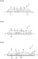
Figs. 3 to 5 are cross-sectional views of slim LED packages according to various embodiments of the present invention; -
Fig. 6 is a cross-sectional view of a slim LED package according to yet another embodiment of the present invention; and -
Fig. 7 is a cross-sectional view taken along line II - II ofFig. 6 . - Exemplary embodiments of the present invention will be described in detail with reference to the accompanying drawings. The embodiments are given by way of illustration for complete understanding of the present invention by those skilled in the art. Hence, the present invention is not limited to these embodiments and can be realized in various forms. Further, for convenience of description, width, length, and thickness of components are not drawn to scale in the drawings. Like components are indicated by like reference numerals throughout the specification.
-
Fig. 1 is a plan view of a slim LED package according to one embodiment of the invention, andFig. 2 is a cross-sectional view taken line I - I ofFig. 1 . - Referring to
Figs. 1 and2 , a slim LED package 1 of this embodiment includes first andsecond lead frames first lead frame 12 has anLED chip 2 mounted thereon, and thesecond lead frame 14 is electrically connected with theLED chip 2 via a bonding wire W. The bonding wire W is connected with thesecond lead frame 14 via a wire ball or soldering ball (not shown). - The first and
second lead frames transparent encapsulation material 20. Thetransparent encapsulation material 20 is formed to entirely cover and protect theLED chip 2 and bonding wire W by molding. Theencapsulation material 20 may be formed by transfer molding with an epoxy molding compound that is a solid epoxy resin. For example, the transfer molding is performed by compressing epoxy molding compound (EMC) powder at a proper pressure into a tablet-shape, followed by positioning and molding the tablet-shaped EMC in a mould at high temperature and pressure conditions to form theencapsulation material 20. - In this embodiment, the
encapsulation material 20 is formed by transfer molding, but the present invention is not limited thereto. Alternatively, theencapsulation material 20 can be formed by injection molding, in which a liquid resin is injected into a mould. Theencapsulation material 20 may be formed of other kinds of transparent resins such as epoxy-based or silicone-based resins, as well as the EMC. - The
first lead frame 12 is formed on an upper surface thereof with achip mounting recess 121, which has theLED chip 2 mounted on a bottom surface thereof in a die-attachment manner. Thechip mounting recess 121 is formed by reducing the thickness of one upper surface region of thefirst lead frame 12 below other regions of thefirst lead frame 12, instead of bending the lead frame to form a reflection cup as in the prior art. Accordingly, thefirst lead frame 12 has a decreased thickness only in the region of thefirst lead frame 12 where theLED chip 2 is mounted, whereby a mounting height of theLED chip 2 is lowered to contribute to slimness of the LED package 1 through an overall thickness reduction of the LED package 1. Further, an inside surface of thechip mounting groove 121 serves as a reflector for reflecting light, thereby enhancing luminescence efficiency of the LED package 1. - The
chip mounting recess 121 may be formed by thickness-etching, which is performed for the purpose of reducing the thickness of the lead frame. At this time, etching can be performed, with the upper surface of thefirst lead frame 12 except for the chip mounting region covered with a mask. Further, thechip mounting recess 121 may have a thickness of about half of the thickness of thefirst lead frame 12. However, it should be noted that the present invention is not limited thereto. - Further, the LED chip 22 may have a thickness less than or equal to the depth of the
chip mounting recess 121 to prevent the height of theLED chip 2 from affecting a thickness increase of the LED package 1. In other words, it is desirable that the depth of thechip mounting recess 121 be set greater than or equal to the height of theLED chip 2. - As clearly shown in
Fig. 2 , the first and second lead frames 12, 14 are respectively formed on lower surfaces thereof withgrooves encapsulation material 20 during the molding process. As a result, the portion of theencapsulation material 20 engages with thegrooves encapsulation material 20 increases, thereby increasing a bonding force between theencapsulation material 20 and the lead frames. Thegrooves - Referring again to
Fig. 2 , theencapsulation material 20 contains aphosphor 202 that is excited by light of a predetermined wavelength and emits light of a different wavelength. Thephosphor 202 contributes to generation of white light through wavelength conversion by converting light emitted from theLED chip 2. In this embodiment, thephosphor 202 is mixed with a resin prepared as a molding material and is disposed in theencapsulation material 20 by the molding process using the molding material. For example, when forming theencapsulation material 20 by transfer molding, a mixture of EMC and thephosphor 202 is prepared and used as the material for the transfer molding. - Next, various other embodiments of the present invention will be described. In description of the embodiments, a repetitious description will be omitted, and, the same or similar elements will be denoted by the same reference numerals as those of the above description.
- In
Fig. 3 , abonding recess 141 is shown, which is formed by reducing the thickness of one upper surface region of asecond lead frame 14 below the thickness of other regions thereof. Thebonding recess 141 can also be formed by the thickness-etching as in the formation of thechip mounting recess 121 of the aforementioned embodiment. At this time, one end of a bonding wire W is connected with thesecond lead frame 14 within thebonding recess 141. - Although not shown in the drawings, a wire ball is located in the
bonding recess 141 such that the one end of the bonding wire W is connected with the wire ball in thebonding recess 141, thereby preventing a thickness increase of the LED package due to the height of the wire ball. A size increase of the wire ball ensures that the bonding wire W can be more rigidly secured to thefirst lead frame 14. Here, the formation of thebonding wire 141 enables more freedom to increase the size of the wire ball. - Referring to
Fig. 4 , in another embodiment of the present invention, aresin 21 containing aphosphor 202 is restrictively provided in thechip mounting recess 121 to cover theLED chip 2 in an adjacent distance. Herein, the resin filling in thechip mounting recess 121 will be defined as an "adjacent resin part." Theadjacent resin part 21 prevents thephosphor 202 from being scattered within theencapsulation material 20, and allows thephosphor 202 to be located around theLED chip 21. This configuration can improve color conversion efficiency by the phosphor, and can provide light consisting of uniformly mixed colors when viewed outside the package. - Alternatively, the
adjacent resin part 21 may not contain the phosphors. For example, the encapsulation material such as epoxy is vulnerable to heat, and can cause thermal deformation or a yellowing phenomenon around theLED chip 2. Here, when theadjacent resin part 21 formed in thechip mounting recess 121 is made of a silicone resin, which is essentially invulnerable to heat, it is possible to efficiently prevent deterioration in performance or lifetime of the LED package caused by the yellowing phenomenon. When using the silicone as a material for theadjacent resin part 21 to prevent thermal deformation or the yellowing phenomenon, thephosphors 202 can be included in theadjacent resin part 21 or omitted therefrom without any influence on the effect of preventing thermal deformation or the yellowing phenomenon. - Alternatively, the
phosphors 202 can be coated on the surface of theLED chip 2 by, for example, conformal coating via electrophoresis. In this case, the LED package 1 has a configuration as illustrated inFig. 5 . -
Fig. 6 is a cross-sectional view of a slim LED package according to yet another embodiment of the present invention, andFig. 7 is a cross-sectional view taken along line II - II ofFig. 6 . - Referring to
Figs. 6 and7 , instead of thegrooves 122, 142 (seeFig. 2 ) of the above embodiment, first and second lead frames 12, 14 of this embodiment are formed withopenings encapsulation material 20 and the lead frames 12, 14. Theopenings - As clearly shown in
Fig. 6 , the first and second lead frames 12, 14 include first andsecond slant parts first slant part 125 is formed on one side of thefirst lead frame 12 facing the other side of thesecond lead frame 14 to be inclined towards right and left sides of thefirst lead frame 12. Further, thesecond slant part 145 is formed on the other side of thesecond lead frame 14 facing the one side of thefirst lead frame 12 to be inclined towards right and left sides of thesecond lead frame 14. The first andsecond slant parts - A portion of the
encapsulation material 20 is interposed between the opposite sides of the first and second lead frames 12, 14 facing each other, and a force is applied to the interposed portion of theencapsulation material 20 and the opposite sides of the first and second lead frames. At this time, theslant parts encapsulation material 20 from being broken on the opposite sides of the lead frames. Furthermore, since theslant part 125 of thefirst lead frame 12 has a shape surrounding the portion of theencapsulation material 20 adjacent thereto, it serves to more rigidly hold theencapsulation material 20. It should be noted that the breakage of theencapsulation material 20 between the opposite sides of the lead frames causes electric short or the like. - Additionally, a
depressed part 126 is formed at the center of the one side of thefirst lead frame 12 facing the other side of the second lead frame to increase a separation between thefirst lead frame 12 and thesecond lead frame 14. Thedepressed part 126 is located directly below a path of the bonding wire W which connects thefirst lead frame 12 with thesecond lead frame 14. Thedepressed part 126 prevents the bonding wire W from being erroneously brought into contact with the lead frames 12, 14, and electric short of the bonding wire W caused by the erroneous contact. - To fabricate the LED packages 1 as described above, a single metal sheet is processed to have a pattern of first and second lead frames 12, 14, followed by molding an encapsulation material on the patterned metal sheet. Then, the lead frames are sawed per each encapsulation material supporting a pair of first and second lead frames 12, 14, thereby providing a plurality of LED packages. At this time, a process of removing burrs formed during sawing may be further included.
- Although the present invention has been described with reference to the embodiments and the accompanying drawings, the present invention is not limited to these embodiments and the drawings. It should be understood that various modifications, additions and substitutions can be made by a person having ordinary knowledge in the art without departing from the scope and spirit of the invention, as defined only by the accompanying claims.
Claims (11)
- A slim light emitting diode (LED) package, comprising:first and second lead frames (12, 14) separated from each other;an LED chip (2) mounted on the first lead frame and electrically connected to the first lead frame and the second lead frame;a wire (W) connecting the LED chip to the second lead frame; anda transparent encapsulation material (20) protecting the LED chip while supporting the first and second lead frames (12, 14)wherein opposing sides of the first lead frames (12, 14) comprises first and second slant parts (125, 145), andwherein the first and second lead frames (12, 14) are formed with openings (123, 143), the openings (123, 143) penetrating the first and second lead frames (12, 14) in the vertical direction..
- The slim LED package of claim 1, wherein the first and second slant parts (125, 145) are formed to face each other in an inclined state.
- The slim LED package of claim 1 or 2, wherein the first and second slant parts (125, 145) have a linear or curved shape.
- The slim LED package of any one of preceding claims, wherein the first slant part (125) is formed to be inclined towards right and left sides of the first lead frame (12)
- The slim LED package of any one of preceding claims, wherein the second slant part (145) is formed to be inclined towards right and left sides of the second lead frame (14).
- The slim LED package of any one of preceding claims, wherein at least one of the opposing sides comprises a depressed portion (126) formed thereon facing the other opposing side.
- The slim LED package of claim 6, wherein the depressed portion (126) is disposed under the wire.
- The slim LED package of claim 6, wherein the depressed portion (126) is formed at the center of the one side of the first lead frame (12) facing the other side of the second lead frame.
- The slim LED package of any one of preceding claims, further comprising a chip mounting recess (121) formed on an upper surface of the first lead frame, wherein the LED chip is disposed in the chip mounting recess.
- The slim LED package of claim 1, wherein a portion of the encapsulation material (20) is interposed between the opposite sides of the first and second lead frames (12, 14) facing each other.
- The slim LED package of claim 10, wherein at least one of the opposing sides has a shape surrounding the portion of the encapsulation material (20) adjacent thereto.
Applications Claiming Priority (3)
| Application Number | Priority Date | Filing Date | Title |
|---|---|---|---|
| KR1020070124469A KR100998233B1 (en) | 2007-12-03 | 2007-12-03 | Slim LED Package |
| EP08856932.2A EP2218116B1 (en) | 2007-12-03 | 2008-11-18 | Slim led package |
| PCT/KR2008/006777 WO2009072757A2 (en) | 2007-12-03 | 2008-11-18 | Slim led package |
Related Parent Applications (2)
| Application Number | Title | Priority Date | Filing Date |
|---|---|---|---|
| EP08856932.2A Division EP2218116B1 (en) | 2007-12-03 | 2008-11-18 | Slim led package |
| EP08856932.2A Division-Into EP2218116B1 (en) | 2007-12-03 | 2008-11-18 | Slim led package |
Publications (3)
| Publication Number | Publication Date |
|---|---|
| EP3444857A1 true EP3444857A1 (en) | 2019-02-20 |
| EP3444857B1 EP3444857B1 (en) | 2024-04-03 |
| EP3444857C0 EP3444857C0 (en) | 2024-04-03 |
Family
ID=40718321
Family Applications (2)
| Application Number | Title | Priority Date | Filing Date |
|---|---|---|---|
| EP18199313.0A Active EP3444857B1 (en) | 2007-12-03 | 2008-11-18 | Slim led package |
| EP08856932.2A Active EP2218116B1 (en) | 2007-12-03 | 2008-11-18 | Slim led package |
Family Applications After (1)
| Application Number | Title | Priority Date | Filing Date |
|---|---|---|---|
| EP08856932.2A Active EP2218116B1 (en) | 2007-12-03 | 2008-11-18 | Slim led package |
Country Status (6)
| Country | Link |
|---|---|
| US (6) | US8319248B2 (en) |
| EP (2) | EP3444857B1 (en) |
| JP (1) | JP5538233B2 (en) |
| KR (1) | KR100998233B1 (en) |
| TW (1) | TWI481070B (en) |
| WO (1) | WO2009072757A2 (en) |
Families Citing this family (80)
| Publication number | Priority date | Publication date | Assignee | Title |
|---|---|---|---|---|
| DE102007046520A1 (en) * | 2007-09-28 | 2009-04-02 | Osram Opto Semiconductors Gmbh | Light-emitting surface element and method for producing a light-emitting surface element |
| JP5206204B2 (en) * | 2008-07-31 | 2013-06-12 | 日亜化学工業株式会社 | Light emitting device |
| US8044420B2 (en) * | 2009-01-15 | 2011-10-25 | Advanced Semiconductor Engineering, Inc. | Light emitting diode package structure |
| DE102009015963A1 (en) * | 2009-04-02 | 2010-10-07 | Osram Opto Semiconductors Gmbh | Optoelectronic component |
| KR101653394B1 (en) * | 2009-06-29 | 2016-09-01 | 서울반도체 주식회사 | Multi chip type light emitting diode package |
| JP5367668B2 (en) * | 2009-11-17 | 2013-12-11 | スタンレー電気株式会社 | Light emitting device and manufacturing method thereof |
| TW201128812A (en) | 2009-12-01 | 2011-08-16 | Lg Innotek Co Ltd | Light emitting device |
| EP2530753A1 (en) * | 2010-01-29 | 2012-12-05 | Kabushiki Kaisha Toshiba | Led package and method for manufacturing same |
| JP5010693B2 (en) | 2010-01-29 | 2012-08-29 | 株式会社東芝 | LED package |
| JP4951090B2 (en) | 2010-01-29 | 2012-06-13 | 株式会社東芝 | LED package |
| JP2011159767A (en) * | 2010-01-29 | 2011-08-18 | Toshiba Corp | Led package and method for manufacturing the same |
| JP5383611B2 (en) | 2010-01-29 | 2014-01-08 | 株式会社東芝 | LED package |
| JP5587625B2 (en) * | 2010-02-01 | 2014-09-10 | アピックヤマダ株式会社 | Lead frame and substrate for LED package |
| JP2011165833A (en) * | 2010-02-08 | 2011-08-25 | Toshiba Corp | Led module |
| JP5691681B2 (en) * | 2010-03-15 | 2015-04-01 | 日亜化学工業株式会社 | Light emitting device |
| TWI561770B (en) | 2010-04-30 | 2016-12-11 | Samsung Electronics Co Ltd | Light emitting device package, light source module, backlight unit, display apparatus, television set, and illumination apparatus |
| KR101719644B1 (en) | 2010-05-24 | 2017-04-04 | 서울반도체 주식회사 | Light emitting diode package |
| DE102010023815A1 (en) | 2010-06-15 | 2011-12-15 | Osram Opto Semiconductors Gmbh | Surface-mountable optoelectronic component and method for producing a surface-mountable optoelectronic component |
| KR101114197B1 (en) * | 2010-08-09 | 2012-02-22 | 엘지이노텍 주식회사 | Light emitting device and lighting system having same |
| EP2613369B1 (en) * | 2010-09-03 | 2020-04-08 | Nichia Corporation | Light emitting device and method for manufacturing same |
| CN102479907B (en) | 2010-11-30 | 2015-01-07 | 展晶科技(深圳)有限公司 | Light emitting diode encapsulation structure |
| KR101825473B1 (en) * | 2011-02-16 | 2018-02-05 | 삼성전자 주식회사 | Light emitting device package and method of fabricating the same |
| KR101823506B1 (en) | 2011-06-29 | 2018-01-30 | 엘지이노텍 주식회사 | Light emitting device and light unit having thereof |
| KR101865272B1 (en) * | 2011-07-26 | 2018-06-07 | 삼성전자주식회사 | Light emitting diode module and method for manufacturing the same |
| KR101294281B1 (en) * | 2011-11-21 | 2013-08-07 | 전자부품연구원 | Semiconductor device having conformal coating thin film and method for manufacturing the same |
| WO2013075309A1 (en) * | 2011-11-24 | 2013-05-30 | Cree Huizhou Solid State Lighting Company Limited | Water resistant led devices and led display including the same |
| KR101979826B1 (en) * | 2011-12-28 | 2019-05-17 | 서울반도체 주식회사 | Light emitting diode package |
| JP6078948B2 (en) | 2012-01-20 | 2017-02-15 | 日亜化学工業株式会社 | Package molded body for light emitting device and light emitting device using the same |
| KR101812741B1 (en) * | 2012-03-09 | 2018-01-30 | 서울바이오시스 주식회사 | Light Emitting Diode Package and Method of manufacturing the same |
| US9240524B2 (en) | 2012-03-05 | 2016-01-19 | Seoul Viosys Co., Ltd. | Light-emitting device and method of manufacturing the same |
| US9653656B2 (en) | 2012-03-16 | 2017-05-16 | Advanced Semiconductor Engineering, Inc. | LED packages and related methods |
| US8637887B2 (en) | 2012-05-08 | 2014-01-28 | Advanced Semiconductor Engineering, Inc. | Thermally enhanced semiconductor packages and related methods |
| KR101957884B1 (en) * | 2012-05-14 | 2019-03-13 | 엘지이노텍 주식회사 | Light emitting device, manufactured method of the light emitting deviceand lighting apparatus |
| JP2013008979A (en) * | 2012-08-02 | 2013-01-10 | Toshiba Corp | Semiconductor package |
| CN103682064B (en) * | 2012-08-31 | 2016-12-07 | 展晶科技(深圳)有限公司 | Side direction LED and method for packing thereof |
| KR101896691B1 (en) * | 2012-10-11 | 2018-09-07 | 엘지이노텍 주식회사 | Light emitting device and lighting system |
| US9059379B2 (en) | 2012-10-29 | 2015-06-16 | Advanced Semiconductor Engineering, Inc. | Light-emitting semiconductor packages and related methods |
| JP6107136B2 (en) | 2012-12-29 | 2017-04-05 | 日亜化学工業株式会社 | LIGHT EMITTING DEVICE PACKAGE, LIGHT EMITTING DEVICE INCLUDING THE SAME, AND LIGHTING DEVICE EQUIPPED WITH THE LIGHT EMITTING DEVICE |
| US9618191B2 (en) | 2013-03-07 | 2017-04-11 | Advanced Semiconductor Engineering, Inc. | Light emitting package and LED bulb |
| JP6476567B2 (en) * | 2013-03-29 | 2019-03-06 | 日亜化学工業株式会社 | Light emitting device |
| JP6303738B2 (en) * | 2013-04-12 | 2018-04-04 | 日亜化学工業株式会社 | Light emitting device |
| US20140346656A1 (en) * | 2013-05-27 | 2014-11-27 | Texas Instruments Incorporated | Multilevel Leadframe |
| KR102042465B1 (en) * | 2013-06-13 | 2019-11-08 | 엘지이노텍 주식회사 | Lighting source module and light system having the same |
| JP6484396B2 (en) | 2013-06-28 | 2019-03-13 | 日亜化学工業株式会社 | Light emitting device package and light emitting device using the same |
| JP6610703B2 (en) * | 2013-06-28 | 2019-11-27 | 日亜化学工業株式会社 | Light emitting device package |
| KR102075730B1 (en) * | 2013-08-07 | 2020-02-10 | 엘지이노텍 주식회사 | Light emitting device and lighting system |
| US9257616B2 (en) | 2013-08-27 | 2016-02-09 | Glo Ab | Molded LED package and method of making same |
| US9142745B2 (en) | 2013-08-27 | 2015-09-22 | Glo Ab | Packaged LED device with castellations |
| US8999737B2 (en) | 2013-08-27 | 2015-04-07 | Glo Ab | Method of making molded LED package |
| JP6210818B2 (en) * | 2013-09-30 | 2017-10-11 | 三菱電機株式会社 | Semiconductor device and manufacturing method thereof |
| TWI610465B (en) | 2013-10-07 | 2018-01-01 | Epistar Corporation | Light-emitting diode assembly and manufacturing method |
| DE102014103034A1 (en) * | 2014-03-07 | 2015-09-10 | Osram Opto Semiconductors Gmbh | Optoelectronic component and method for its production |
| JP6262578B2 (en) * | 2014-03-18 | 2018-01-17 | スタンレー電気株式会社 | Light emitting device |
| KR102160075B1 (en) | 2014-04-22 | 2020-09-25 | 서울반도체 주식회사 | Light emitting device |
| JP6535509B2 (en) * | 2014-05-12 | 2019-06-26 | ローム株式会社 | Semiconductor device |
| US9431327B2 (en) | 2014-05-30 | 2016-08-30 | Delta Electronics, Inc. | Semiconductor device |
| CN105280780A (en) * | 2014-07-10 | 2016-01-27 | 邱罗利士公司 | Packaging structure and its manufacturing method and carrier |
| JP6413412B2 (en) | 2014-07-11 | 2018-10-31 | 日亜化学工業株式会社 | Semiconductor light emitting device and manufacturing method thereof |
| KR20160023011A (en) * | 2014-08-20 | 2016-03-03 | 삼성전자주식회사 | Light emitting device package |
| TWI570352B (en) * | 2014-11-28 | 2017-02-11 | 宏齊科技股份有限公司 | Light-emitting diode device and light-emitting device using same |
| JP6206442B2 (en) * | 2015-04-30 | 2017-10-04 | 日亜化学工業株式会社 | Package, method for manufacturing the same, and light emitting device |
| US10099800B2 (en) * | 2015-05-08 | 2018-10-16 | The Boeing Company | Structurally embedded lighting for display panels and method of making the same |
| CN107615477B (en) * | 2015-06-18 | 2021-12-28 | 京瓷株式会社 | Substrate for mounting electronic component and electronic device |
| JP6015842B2 (en) * | 2015-12-03 | 2016-10-26 | 大日本印刷株式会社 | Lead frame for optical semiconductor device, lead frame for optical semiconductor device with resin, multi-sided body of lead frame, multi-sided body of lead frame with resin, optical semiconductor device, multi-sided body of optical semiconductor device |
| WO2017135744A1 (en) * | 2016-02-05 | 2017-08-10 | 엘지이노텍(주) | Light-emitting element package |
| EP3223322B1 (en) * | 2016-03-25 | 2019-05-01 | LG Innotek Co., Ltd. | Light emitting device package |
| KR102479946B1 (en) * | 2016-04-06 | 2022-12-22 | 해성디에스 주식회사 | Semiconductor Package substrate and manufacturing method thereof |
| CN105938866A (en) * | 2016-06-13 | 2016-09-14 | 开发晶照明(厦门)有限公司 | LED bracket and LED package structure |
| JP6857035B2 (en) * | 2017-01-12 | 2021-04-14 | ローム株式会社 | Semiconductor device |
| JP6806925B2 (en) * | 2017-04-04 | 2021-01-06 | シグニファイ ホールディング ビー ヴィSignify Holding B.V. | Manufacturing method of solid-state light emitter package, lamp, luminaire, and solid-state light emitter package |
| CN111279471B (en) * | 2017-11-10 | 2023-09-15 | 新电元工业株式会社 | electronic module |
| JP6560819B1 (en) * | 2017-11-10 | 2019-08-14 | 新電元工業株式会社 | Electronic module and method for manufacturing electronic module |
| JP6879262B2 (en) * | 2018-05-08 | 2021-06-02 | 日亜化学工業株式会社 | Light emitting device |
| CN109285935A (en) * | 2018-11-07 | 2019-01-29 | 东莞市亿晶源光电科技有限公司 | Whole-body light-emitting LED lamp bead and lamp string |
| CN110416201B (en) * | 2019-08-28 | 2024-12-31 | 东莞市欧思科光电科技有限公司 | LED structure with built-in IC |
| CN110649144A (en) * | 2019-09-25 | 2020-01-03 | 广东晶科电子股份有限公司 | A kind of LED device and its packaging bracket |
| DE102022114582A1 (en) * | 2022-06-09 | 2023-12-14 | Ams-Osram International Gmbh | OPTOELECTRONIC COMPONENT AND METHOD FOR PRODUCING AN OPTOELECTRONIC COMPONENT |
| CN115172316A (en) * | 2022-06-29 | 2022-10-11 | 星科金朋半导体(江阴)有限公司 | Semiconductor packaging structure and preparation method |
| CN114824040B (en) * | 2022-07-01 | 2022-11-08 | 广东中科半导体微纳制造技术研究院 | Semiconductor package device |
| WO2025217899A1 (en) * | 2024-04-19 | 2025-10-23 | Ams-Osram International Gmbh | Electronic component and method for manufacturing an electronic component |
Citations (5)
| Publication number | Priority date | Publication date | Assignee | Title |
|---|---|---|---|---|
| US20020066905A1 (en) * | 2000-06-20 | 2002-06-06 | Bily Wang | Wing-shaped surface mount package for light emitting diodes |
| US20030107316A1 (en) * | 2001-12-07 | 2003-06-12 | Gen Murakami | Light-emitting unit and method for producing same as well as lead frame used for producing light-emitting unit |
| US20050151149A1 (en) * | 2004-01-08 | 2005-07-14 | Chia Chee W. | Light emission device |
| US20050280017A1 (en) * | 2004-06-11 | 2005-12-22 | Kabushiki Kaisha Toshiba | Semiconductor light emitting device and semiconductor light emitting unit |
| US20060220048A1 (en) * | 2005-03-30 | 2006-10-05 | Kabushiki Kaisha Toshiba | Semiconductor light emitting device and semiconductor light emitting unit |
Family Cites Families (53)
| Publication number | Priority date | Publication date | Assignee | Title |
|---|---|---|---|---|
| JPS5558557A (en) * | 1978-10-25 | 1980-05-01 | Hitachi Ltd | Resin mold type electronic component and lead frame used therefor |
| JPS5766550U (en) * | 1980-10-06 | 1982-04-21 | ||
| JPS62140758A (en) | 1985-12-16 | 1987-06-24 | Kobe Steel Ltd | Mechanical wire cut saw |
| JPH0429580Y2 (en) * | 1986-02-28 | 1992-07-17 | ||
| JPS63200550A (en) * | 1987-02-17 | 1988-08-18 | Matsushita Electronics Corp | Lead frame |
| JPH02125454A (en) * | 1988-11-02 | 1990-05-14 | Nec Corp | Resin-sealed semiconductor device |
| JPH038459A (en) | 1989-06-05 | 1991-01-16 | Geinzu:Kk | Shower head |
| JPH038459U (en) * | 1989-06-12 | 1991-01-28 | ||
| JPH04242966A (en) * | 1990-08-09 | 1992-08-31 | Fuji Electric Co Ltd | Resin sealed semiconductor device |
| TW383508B (en) * | 1996-07-29 | 2000-03-01 | Nichia Kagaku Kogyo Kk | Light emitting device and display |
| TW414924B (en) * | 1998-05-29 | 2000-12-11 | Rohm Co Ltd | Semiconductor device of resin package |
| JP2001085747A (en) * | 1999-09-13 | 2001-03-30 | Sanken Electric Co Ltd | Semiconductor light emitting device |
| TW433551U (en) * | 1999-10-26 | 2001-05-01 | You Shang Hua | Improvement of cup base for light emitting diode chip |
| JP2001210872A (en) * | 2000-01-26 | 2001-08-03 | Sanyo Electric Co Ltd | Semiconductor light emitting device and method of manufacturing the same |
| DE10041328B4 (en) | 2000-08-23 | 2018-04-05 | Osram Opto Semiconductors Gmbh | Packaging unit for semiconductor chips |
| JP3614776B2 (en) * | 2000-12-19 | 2005-01-26 | シャープ株式会社 | Chip component type LED and its manufacturing method |
| KR20020065729A (en) | 2001-02-07 | 2002-08-14 | 주식회사 칩팩코리아 | Semicoductor package |
| JP3753011B2 (en) | 2001-04-11 | 2006-03-08 | 豊田合成株式会社 | Reflective light emitting diode |
| WO2003021691A1 (en) * | 2001-09-03 | 2003-03-13 | Matsushita Electric Industrial Co., Ltd. | Semiconductor light emitting device, light emitting apparatus and production method for semiconductor light emitting device |
| EP1939939A3 (en) * | 2002-06-14 | 2010-03-24 | Lednium Technology Pty Limited | A lamp and method of producing a lamp |
| US6717353B1 (en) * | 2002-10-14 | 2004-04-06 | Lumileds Lighting U.S., Llc | Phosphor converted light emitting device |
| JP2006313943A (en) * | 2003-02-18 | 2006-11-16 | Sharp Corp | Semiconductor light emitting device, method for manufacturing the same, and electronic imaging device |
| JP3910171B2 (en) * | 2003-02-18 | 2007-04-25 | シャープ株式会社 | Semiconductor light emitting device, method for manufacturing the same, and electronic imaging device |
| US7718451B2 (en) * | 2003-02-28 | 2010-05-18 | Osram Opto Semiconductor Gmbh | Method for producing an optoelectronic device with patterned-metallized package body and method for the patterned metalization of a plastic-containing body |
| EP1603170B1 (en) | 2003-03-10 | 2018-08-01 | Toyoda Gosei Co., Ltd. | Method for manufacturing a solid-state optical element device |
| US6933535B2 (en) | 2003-10-31 | 2005-08-23 | Lumileds Lighting U.S., Llc | Light emitting devices with enhanced luminous efficiency |
| JP3967314B2 (en) * | 2003-12-12 | 2007-08-29 | ローム株式会社 | Light emitting element |
| JP2005197329A (en) * | 2004-01-05 | 2005-07-21 | Stanley Electric Co Ltd | Surface mount semiconductor device and lead frame structure thereof |
| JP2005317661A (en) * | 2004-04-27 | 2005-11-10 | Sharp Corp | Semiconductor light emitting device and manufacturing method thereof |
| KR100665299B1 (en) | 2004-06-10 | 2007-01-04 | 서울반도체 주식회사 | Emitting material |
| EP1794808B1 (en) * | 2004-09-10 | 2017-08-09 | Seoul Semiconductor Co., Ltd. | Light emitting diode package having multiple molding resins |
| KR20060059575A (en) | 2004-11-29 | 2006-06-02 | 삼성전자주식회사 | Semiconductor package with fine protrusions on die pad |
| IL165484A0 (en) | 2004-11-30 | 2006-01-15 | Applied Research Systems | Production of proteins |
| JP2006179541A (en) | 2004-12-21 | 2006-07-06 | Enomoto Co Ltd | Power LED lead frame and manufacturing method thereof |
| CN101138278A (en) | 2005-03-09 | 2008-03-05 | 皇家飞利浦电子股份有限公司 | Illumination systems including radiation sources and fluorescent materials |
| US7341878B2 (en) * | 2005-03-14 | 2008-03-11 | Philips Lumileds Lighting Company, Llc | Wavelength-converted semiconductor light emitting device |
| US7211882B2 (en) * | 2005-03-22 | 2007-05-01 | Harvatek Corporation | LED package structure and method for making the same |
| US7445730B2 (en) * | 2005-03-31 | 2008-11-04 | Dowa Electronics Materials Co., Ltd. | Phosphor and manufacturing method of the same, and light emitting device using the phosphor |
| JP2007110060A (en) * | 2005-09-15 | 2007-04-26 | Nichia Chem Ind Ltd | Light emitting device |
| JP5118837B2 (en) | 2005-10-25 | 2013-01-16 | インテマティックス・コーポレーション | Silicate orange phosphor |
| KR100828891B1 (en) * | 2006-02-23 | 2008-05-09 | 엘지이노텍 주식회사 | LED Package |
| WO2007127029A2 (en) * | 2006-04-24 | 2007-11-08 | Cree, Inc. | Side-view surface mount white led |
| US7960819B2 (en) * | 2006-07-13 | 2011-06-14 | Cree, Inc. | Leadframe-based packages for solid state emitting devices |
| KR100851636B1 (en) * | 2006-07-27 | 2008-08-13 | 삼성전기주식회사 | Surface-Mount LED Elements |
| JP5168152B2 (en) * | 2006-12-28 | 2013-03-21 | 日亜化学工業株式会社 | Light emitting device |
| US7800304B2 (en) * | 2007-01-12 | 2010-09-21 | Avago Technologies Ecbu Ip (Singapore) Pte. Ltd. | Multi-chip packaged LED light source |
| TW200834968A (en) * | 2007-02-13 | 2008-08-16 | Harvatek Corp | Method of making light-emitting diode structure with high heat dissipation effect and structure made thereby |
| US7514724B2 (en) * | 2007-03-23 | 2009-04-07 | Avago Technologies Ecbu Ip (Singapore) Pte. Ltd. | Solid state light source having a variable number of dies |
| KR100811723B1 (en) * | 2007-03-30 | 2008-03-11 | 서울반도체 주식회사 | LED Package |
| JP5122172B2 (en) * | 2007-03-30 | 2013-01-16 | ローム株式会社 | Semiconductor light emitting device |
| US7923831B2 (en) * | 2007-05-31 | 2011-04-12 | Avago Technologies Ecbu Ip (Singapore) Pte. Ltd. | LED-based light source having improved thermal dissipation |
| JP5578597B2 (en) * | 2007-09-03 | 2014-08-27 | 独立行政法人物質・材料研究機構 | Phosphor, method for manufacturing the same, and light emitting device using the same |
| KR100888236B1 (en) * | 2008-11-18 | 2009-03-12 | 서울반도체 주식회사 | Light emitting device |
-
2007
- 2007-12-03 KR KR1020070124469A patent/KR100998233B1/en active Active
-
2008
- 2008-11-18 JP JP2010535872A patent/JP5538233B2/en active Active
- 2008-11-18 US US12/745,878 patent/US8319248B2/en not_active Expired - Fee Related
- 2008-11-18 EP EP18199313.0A patent/EP3444857B1/en active Active
- 2008-11-18 EP EP08856932.2A patent/EP2218116B1/en active Active
- 2008-11-18 WO PCT/KR2008/006777 patent/WO2009072757A2/en not_active Ceased
- 2008-12-02 TW TW097146765A patent/TWI481070B/en active
-
2012
- 2012-09-28 US US13/631,060 patent/US8659050B2/en active Active
-
2014
- 2014-01-22 US US14/161,377 patent/US8963196B2/en active Active
-
2015
- 2015-02-17 US US14/624,172 patent/US9412913B2/en active Active
- 2015-08-03 US US14/816,532 patent/US9530942B2/en active Active - Reinstated
-
2016
- 2016-11-16 US US15/352,726 patent/US9899573B2/en not_active Expired - Fee Related
Patent Citations (5)
| Publication number | Priority date | Publication date | Assignee | Title |
|---|---|---|---|---|
| US20020066905A1 (en) * | 2000-06-20 | 2002-06-06 | Bily Wang | Wing-shaped surface mount package for light emitting diodes |
| US20030107316A1 (en) * | 2001-12-07 | 2003-06-12 | Gen Murakami | Light-emitting unit and method for producing same as well as lead frame used for producing light-emitting unit |
| US20050151149A1 (en) * | 2004-01-08 | 2005-07-14 | Chia Chee W. | Light emission device |
| US20050280017A1 (en) * | 2004-06-11 | 2005-12-22 | Kabushiki Kaisha Toshiba | Semiconductor light emitting device and semiconductor light emitting unit |
| US20060220048A1 (en) * | 2005-03-30 | 2006-10-05 | Kabushiki Kaisha Toshiba | Semiconductor light emitting device and semiconductor light emitting unit |
Also Published As
| Publication number | Publication date |
|---|---|
| EP2218116A2 (en) | 2010-08-18 |
| US20150340570A1 (en) | 2015-11-26 |
| US9530942B2 (en) | 2016-12-27 |
| JP5538233B2 (en) | 2014-07-02 |
| US9412913B2 (en) | 2016-08-09 |
| KR20090057755A (en) | 2009-06-08 |
| WO2009072757A2 (en) | 2009-06-11 |
| US20150162514A1 (en) | 2015-06-11 |
| EP3444857B1 (en) | 2024-04-03 |
| US20170062665A1 (en) | 2017-03-02 |
| JP2011505689A (en) | 2011-02-24 |
| US8659050B2 (en) | 2014-02-25 |
| EP3444857C0 (en) | 2024-04-03 |
| US20100270571A1 (en) | 2010-10-28 |
| US8963196B2 (en) | 2015-02-24 |
| US9899573B2 (en) | 2018-02-20 |
| EP2218116B1 (en) | 2019-01-09 |
| TW200939541A (en) | 2009-09-16 |
| US20140131762A1 (en) | 2014-05-15 |
| US20130020604A1 (en) | 2013-01-24 |
| KR100998233B1 (en) | 2010-12-07 |
| TWI481070B (en) | 2015-04-11 |
| US8319248B2 (en) | 2012-11-27 |
| WO2009072757A3 (en) | 2009-08-06 |
| EP2218116A4 (en) | 2012-04-04 |
Similar Documents
| Publication | Publication Date | Title |
|---|---|---|
| EP3444857B1 (en) | Slim led package | |
| US20060157828A1 (en) | Leadframe - based housing, leadframe strip, surface - mounted optoelectronic -component, and production method | |
| JP2009177187A (en) | Light emitting diode package | |
| CN101997075A (en) | Light emitting device and method of manufacturing light emitting device | |
| CN102203940A (en) | Support body for semiconductor component, semiconductor component and method for producing the support body | |
| KR101669281B1 (en) | Light-emitting device | |
| US7666715B2 (en) | Radiation-emitting and/or radiation-receiving semiconductor component and method for the production thereof | |
| JP4939946B2 (en) | Beam emitting type and / or beam receiving type semiconductor component | |
| TWI569475B (en) | Light-emitting device, circuit substrate, package array for light-emitting device, and manufacturing method of package array for light-emitting device | |
| EP2674994A1 (en) | Light emitting device, method for manufacturing light emitting device, and package array | |
| JP5097372B2 (en) | High-current, high-efficiency surface-mount light-emitting diode lamp and method for manufacturing the same | |
| KR101778141B1 (en) | Semiconductor light emitting device and method of manufacturing the same | |
| KR101104253B1 (en) | LED package and LED leadframe | |
| KR20110119200A (en) | Light emitting device | |
| KR101863549B1 (en) | Semiconductor light emitting device | |
| JP5722759B2 (en) | Light emitting device | |
| KR20110080902A (en) | LED Package | |
| KR101855189B1 (en) | Semiconductor light emitting device | |
| US20070181899A1 (en) | Light emitting diode package | |
| KR20170136473A (en) | Semiconductor light emitting device | |
| KR20170113730A (en) | Semiconductor light emitting device |
Legal Events
| Date | Code | Title | Description |
|---|---|---|---|
| PUAI | Public reference made under article 153(3) epc to a published international application that has entered the european phase |
Free format text: ORIGINAL CODE: 0009012 |
|
| STAA | Information on the status of an ep patent application or granted ep patent |
Free format text: STATUS: REQUEST FOR EXAMINATION WAS MADE |
|
| 17P | Request for examination filed |
Effective date: 20181009 |
|
| AC | Divisional application: reference to earlier application |
Ref document number: 2218116 Country of ref document: EP Kind code of ref document: P |
|
| AK | Designated contracting states |
Kind code of ref document: A1 Designated state(s): AT BE BG CH CY CZ DE DK EE ES FI FR GB GR HR HU IE IS IT LI LT LU LV MC MT NL NO PL PT RO SE SI SK TR |
|
| STAA | Information on the status of an ep patent application or granted ep patent |
Free format text: STATUS: EXAMINATION IS IN PROGRESS |
|
| 17Q | First examination report despatched |
Effective date: 20210715 |
|
| GRAP | Despatch of communication of intention to grant a patent |
Free format text: ORIGINAL CODE: EPIDOSNIGR1 |
|
| STAA | Information on the status of an ep patent application or granted ep patent |
Free format text: STATUS: GRANT OF PATENT IS INTENDED |
|
| INTG | Intention to grant announced |
Effective date: 20231121 |
|
| RIN1 | Information on inventor provided before grant (corrected) |
Inventor name: SEO, EUN JUNG |
|
| GRAS | Grant fee paid |
Free format text: ORIGINAL CODE: EPIDOSNIGR3 |
|
| GRAA | (expected) grant |
Free format text: ORIGINAL CODE: 0009210 |
|
| STAA | Information on the status of an ep patent application or granted ep patent |
Free format text: STATUS: THE PATENT HAS BEEN GRANTED |
|
| AC | Divisional application: reference to earlier application |
Ref document number: 2218116 Country of ref document: EP Kind code of ref document: P |
|
| AK | Designated contracting states |
Kind code of ref document: B1 Designated state(s): AT BE BG CH CY CZ DE DK EE ES FI FR GB GR HR HU IE IS IT LI LT LU LV MC MT NL NO PL PT RO SE SI SK TR |
|
| REG | Reference to a national code |
Ref country code: GB Ref legal event code: FG4D |
|
| REG | Reference to a national code |
Ref country code: CH Ref legal event code: EP |
|
| REG | Reference to a national code |
Ref country code: IE Ref legal event code: FG4D |
|
| REG | Reference to a national code |
Ref country code: DE Ref legal event code: R096 Ref document number: 602008064993 Country of ref document: DE |
|
| U01 | Request for unitary effect filed |
Effective date: 20240411 |
|
| U07 | Unitary effect registered |
Designated state(s): AT BE BG DE DK EE FI FR IT LT LU LV MT NL PT SE SI Effective date: 20240419 |
|
| PG25 | Lapsed in a contracting state [announced via postgrant information from national office to epo] |
Ref country code: IS Free format text: LAPSE BECAUSE OF FAILURE TO SUBMIT A TRANSLATION OF THE DESCRIPTION OR TO PAY THE FEE WITHIN THE PRESCRIBED TIME-LIMIT Effective date: 20240803 |
|
| PG25 | Lapsed in a contracting state [announced via postgrant information from national office to epo] |
Ref country code: HR Free format text: LAPSE BECAUSE OF FAILURE TO SUBMIT A TRANSLATION OF THE DESCRIPTION OR TO PAY THE FEE WITHIN THE PRESCRIBED TIME-LIMIT Effective date: 20240403 |
|
| PG25 | Lapsed in a contracting state [announced via postgrant information from national office to epo] |
Ref country code: GR Free format text: LAPSE BECAUSE OF FAILURE TO SUBMIT A TRANSLATION OF THE DESCRIPTION OR TO PAY THE FEE WITHIN THE PRESCRIBED TIME-LIMIT Effective date: 20240704 |
|
| PG25 | Lapsed in a contracting state [announced via postgrant information from national office to epo] |
Ref country code: ES Free format text: LAPSE BECAUSE OF FAILURE TO SUBMIT A TRANSLATION OF THE DESCRIPTION OR TO PAY THE FEE WITHIN THE PRESCRIBED TIME-LIMIT Effective date: 20240403 |
|
| PG25 | Lapsed in a contracting state [announced via postgrant information from national office to epo] |
Ref country code: CZ Free format text: LAPSE BECAUSE OF FAILURE TO SUBMIT A TRANSLATION OF THE DESCRIPTION OR TO PAY THE FEE WITHIN THE PRESCRIBED TIME-LIMIT Effective date: 20240403 |
|
| PG25 | Lapsed in a contracting state [announced via postgrant information from national office to epo] |
Ref country code: PL Free format text: LAPSE BECAUSE OF FAILURE TO SUBMIT A TRANSLATION OF THE DESCRIPTION OR TO PAY THE FEE WITHIN THE PRESCRIBED TIME-LIMIT Effective date: 20240403 |
|
| PG25 | Lapsed in a contracting state [announced via postgrant information from national office to epo] |
Ref country code: PL Free format text: LAPSE BECAUSE OF FAILURE TO SUBMIT A TRANSLATION OF THE DESCRIPTION OR TO PAY THE FEE WITHIN THE PRESCRIBED TIME-LIMIT Effective date: 20240403 Ref country code: NO Free format text: LAPSE BECAUSE OF FAILURE TO SUBMIT A TRANSLATION OF THE DESCRIPTION OR TO PAY THE FEE WITHIN THE PRESCRIBED TIME-LIMIT Effective date: 20240703 Ref country code: IS Free format text: LAPSE BECAUSE OF FAILURE TO SUBMIT A TRANSLATION OF THE DESCRIPTION OR TO PAY THE FEE WITHIN THE PRESCRIBED TIME-LIMIT Effective date: 20240803 Ref country code: HR Free format text: LAPSE BECAUSE OF FAILURE TO SUBMIT A TRANSLATION OF THE DESCRIPTION OR TO PAY THE FEE WITHIN THE PRESCRIBED TIME-LIMIT Effective date: 20240403 Ref country code: GR Free format text: LAPSE BECAUSE OF FAILURE TO SUBMIT A TRANSLATION OF THE DESCRIPTION OR TO PAY THE FEE WITHIN THE PRESCRIBED TIME-LIMIT Effective date: 20240704 Ref country code: ES Free format text: LAPSE BECAUSE OF FAILURE TO SUBMIT A TRANSLATION OF THE DESCRIPTION OR TO PAY THE FEE WITHIN THE PRESCRIBED TIME-LIMIT Effective date: 20240403 Ref country code: CZ Free format text: LAPSE BECAUSE OF FAILURE TO SUBMIT A TRANSLATION OF THE DESCRIPTION OR TO PAY THE FEE WITHIN THE PRESCRIBED TIME-LIMIT Effective date: 20240403 |
|
| U20 | Renewal fee for the european patent with unitary effect paid |
Year of fee payment: 17 Effective date: 20241122 |
|
| REG | Reference to a national code |
Ref country code: DE Ref legal event code: R097 Ref document number: 602008064993 Country of ref document: DE |
|
| PG25 | Lapsed in a contracting state [announced via postgrant information from national office to epo] |
Ref country code: RO Free format text: LAPSE BECAUSE OF FAILURE TO SUBMIT A TRANSLATION OF THE DESCRIPTION OR TO PAY THE FEE WITHIN THE PRESCRIBED TIME-LIMIT Effective date: 20240403 Ref country code: SK Free format text: LAPSE BECAUSE OF FAILURE TO SUBMIT A TRANSLATION OF THE DESCRIPTION OR TO PAY THE FEE WITHIN THE PRESCRIBED TIME-LIMIT Effective date: 20240403 |
|
| PG25 | Lapsed in a contracting state [announced via postgrant information from national office to epo] |
Ref country code: SK Free format text: LAPSE BECAUSE OF FAILURE TO SUBMIT A TRANSLATION OF THE DESCRIPTION OR TO PAY THE FEE WITHIN THE PRESCRIBED TIME-LIMIT Effective date: 20240403 Ref country code: RO Free format text: LAPSE BECAUSE OF FAILURE TO SUBMIT A TRANSLATION OF THE DESCRIPTION OR TO PAY THE FEE WITHIN THE PRESCRIBED TIME-LIMIT Effective date: 20240403 |
|
| PLBE | No opposition filed within time limit |
Free format text: ORIGINAL CODE: 0009261 |
|
| STAA | Information on the status of an ep patent application or granted ep patent |
Free format text: STATUS: NO OPPOSITION FILED WITHIN TIME LIMIT |
|
| 26N | No opposition filed |
Effective date: 20250106 |
|
| REG | Reference to a national code |
Ref country code: CH Ref legal event code: PL |
|
| PG25 | Lapsed in a contracting state [announced via postgrant information from national office to epo] |
Ref country code: MC Free format text: LAPSE BECAUSE OF FAILURE TO SUBMIT A TRANSLATION OF THE DESCRIPTION OR TO PAY THE FEE WITHIN THE PRESCRIBED TIME-LIMIT Effective date: 20240403 |
|
| REG | Reference to a national code |
Ref country code: CH Ref legal event code: PL |
|
| GBPC | Gb: european patent ceased through non-payment of renewal fee |
Effective date: 20241118 |
|
| PG25 | Lapsed in a contracting state [announced via postgrant information from national office to epo] |
Ref country code: CH Free format text: LAPSE BECAUSE OF NON-PAYMENT OF DUE FEES Effective date: 20241130 |
|
| PG25 | Lapsed in a contracting state [announced via postgrant information from national office to epo] |
Ref country code: GB Free format text: LAPSE BECAUSE OF NON-PAYMENT OF DUE FEES Effective date: 20241118 |
|
| PG25 | Lapsed in a contracting state [announced via postgrant information from national office to epo] |
Ref country code: IE Free format text: LAPSE BECAUSE OF NON-PAYMENT OF DUE FEES Effective date: 20241118 |
|
| U20 | Renewal fee for the european patent with unitary effect paid |
Year of fee payment: 18 Effective date: 20251124 |
|
| PG25 | Lapsed in a contracting state [announced via postgrant information from national office to epo] |
Ref country code: HU Free format text: LAPSE BECAUSE OF FAILURE TO SUBMIT A TRANSLATION OF THE DESCRIPTION OR TO PAY THE FEE WITHIN THE PRESCRIBED TIME-LIMIT; INVALID AB INITIO Effective date: 20081118 |
|
| PG25 | Lapsed in a contracting state [announced via postgrant information from national office to epo] |
Ref country code: CY Free format text: LAPSE BECAUSE OF FAILURE TO SUBMIT A TRANSLATION OF THE DESCRIPTION OR TO PAY THE FEE WITHIN THE PRESCRIBED TIME-LIMIT; INVALID AB INITIO Effective date: 20081118 |