EP3441484A1 - Supraleitender stabilisator - Google Patents
Supraleitender stabilisator Download PDFInfo
- Publication number
- EP3441484A1 EP3441484A1 EP17779088.8A EP17779088A EP3441484A1 EP 3441484 A1 EP3441484 A1 EP 3441484A1 EP 17779088 A EP17779088 A EP 17779088A EP 3441484 A1 EP3441484 A1 EP 3441484A1
- Authority
- EP
- European Patent Office
- Prior art keywords
- mass
- ppm
- less
- amount
- superconductor
- Prior art date
- Legal status (The legal status is an assumption and is not a legal conclusion. Google has not performed a legal analysis and makes no representation as to the accuracy of the status listed.)
- Granted
Links
Images

Classifications
-
- C—CHEMISTRY; METALLURGY
- C22—METALLURGY; FERROUS OR NON-FERROUS ALLOYS; TREATMENT OF ALLOYS OR NON-FERROUS METALS
- C22C—ALLOYS
- C22C9/00—Alloys based on copper
-
- C—CHEMISTRY; METALLURGY
- C22—METALLURGY; FERROUS OR NON-FERROUS ALLOYS; TREATMENT OF ALLOYS OR NON-FERROUS METALS
- C22F—CHANGING THE PHYSICAL STRUCTURE OF NON-FERROUS METALS AND NON-FERROUS ALLOYS
- C22F1/00—Changing the physical structure of non-ferrous metals or alloys by heat treatment or by hot or cold working
- C22F1/08—Changing the physical structure of non-ferrous metals or alloys by heat treatment or by hot or cold working of copper or alloys based thereon
-
- H—ELECTRICITY
- H01—ELECTRIC ELEMENTS
- H01B—CABLES; CONDUCTORS; INSULATORS; SELECTION OF MATERIALS FOR THEIR CONDUCTIVE, INSULATING OR DIELECTRIC PROPERTIES
- H01B1/00—Conductors or conductive bodies characterised by the conductive materials; Selection of materials as conductors
- H01B1/02—Conductors or conductive bodies characterised by the conductive materials; Selection of materials as conductors mainly consisting of metals or alloys
- H01B1/026—Alloys based on copper
-
- H—ELECTRICITY
- H01—ELECTRIC ELEMENTS
- H01B—CABLES; CONDUCTORS; INSULATORS; SELECTION OF MATERIALS FOR THEIR CONDUCTIVE, INSULATING OR DIELECTRIC PROPERTIES
- H01B12/00—Superconductive or hyperconductive conductors, cables, or transmission lines
- H01B12/02—Superconductive or hyperconductive conductors, cables, or transmission lines characterised by their form
- H01B12/10—Multi-filaments embedded in normal conductors
-
- H—ELECTRICITY
- H10—SEMICONDUCTOR DEVICES; ELECTRIC SOLID-STATE DEVICES NOT OTHERWISE PROVIDED FOR
- H10N—ELECTRIC SOLID-STATE DEVICES NOT OTHERWISE PROVIDED FOR
- H10N60/00—Superconducting devices
- H10N60/10—Junction-based devices
-
- H—ELECTRICITY
- H10—SEMICONDUCTOR DEVICES; ELECTRIC SOLID-STATE DEVICES NOT OTHERWISE PROVIDED FOR
- H10N—ELECTRIC SOLID-STATE DEVICES NOT OTHERWISE PROVIDED FOR
- H10N60/00—Superconducting devices
- H10N60/80—Constructional details
- H10N60/85—Superconducting active materials
-
- H—ELECTRICITY
- H01—ELECTRIC ELEMENTS
- H01F—MAGNETS; INDUCTANCES; TRANSFORMERS; SELECTION OF MATERIALS FOR THEIR MAGNETIC PROPERTIES
- H01F6/00—Superconducting magnets; Superconducting coils
- H01F6/06—Coils, e.g. winding, insulating, terminating or casing arrangements therefor
-
- H—ELECTRICITY
- H02—GENERATION; CONVERSION OR DISTRIBUTION OF ELECTRIC POWER
- H02K—DYNAMO-ELECTRIC MACHINES
- H02K3/00—Details of windings
- H02K3/02—Windings characterised by the conductor material
-
- Y—GENERAL TAGGING OF NEW TECHNOLOGICAL DEVELOPMENTS; GENERAL TAGGING OF CROSS-SECTIONAL TECHNOLOGIES SPANNING OVER SEVERAL SECTIONS OF THE IPC; TECHNICAL SUBJECTS COVERED BY FORMER USPC CROSS-REFERENCE ART COLLECTIONS [XRACs] AND DIGESTS
- Y02—TECHNOLOGIES OR APPLICATIONS FOR MITIGATION OR ADAPTATION AGAINST CLIMATE CHANGE
- Y02E—REDUCTION OF GREENHOUSE GAS [GHG] EMISSIONS, RELATED TO ENERGY GENERATION, TRANSMISSION OR DISTRIBUTION
- Y02E40/00—Technologies for an efficient electrical power generation, transmission or distribution
- Y02E40/60—Superconducting electric elements or equipment; Power systems integrating superconducting elements or equipment
Definitions
- the present invention relates to a stabilizer material for superconductor (superconducting stabilizer) used for a superconducting wire, a superconducting wire including the stabilizer material for superconductor, and a superconducting coil including the superconducting wire.
- the superconducting wire described above is, for example, used in fields such as MRI, NMR, particle accelerators, maglev trains, and power storage apparatuses.
- This superconducting wire has a multi-core structure in which a plurality of strands consisting of a superconducting material such as Nb-Ti or Nb 3 Sn are bundled with a stabilizer material for superconductor interposed therebetween.
- a tape-shaped superconducting wire in which a superconducting material and a stabilizer material for superconductor are laminated is also provided.
- a superconducting wire in which strands are incorporated in a channel member consisting of pure copper is also provided.
- a stabilizer material for superconductor having a comparatively low resistance such as copper is arranged so as to be in contact with the superconducting material (strands).
- the current flowing through the superconducting material is temporarily bypassed to the stabilizer material for superconductor and the superconducting material is cooled to return to the superconducting state in the meantime.
- the structure of the superconducting wire consists of wire strands of the superconducting material represented by Nb-Ti or Nb 3 Sn and the stabilizer material for superconductor consisting of a copper material which are processed so as to be in contact with each other, and in which the plurality of strands including the superconducting material and the stabilizer material for superconductor are processed to be a single structural body.
- This process includes extrusion, rolling, wire drawing, drawing, and twisting.
- Residual resistance ratio is widely used as an indicator of electric resistance at extremely low temperatures.
- the residual resistance ratio (RRR) is the ratio ⁇ 293K / ⁇ 4.2K of the electrical resistivity ⁇ 293K at room temperature (293 K) to the electrical resistivity ⁇ 4.2K at the temperature of liquid helium (4.2 K), and the higher the residual resistance ratio (RRR) is, the better the performance as a stabilizer material for superconductor is exhibited.
- Patent Documents 1 to 3 propose a Cu material having a high residual resistance ratio (RRR).
- Patent Document 1 discloses that a copper material having a high residual resistance ratio (RRR) is obtained by heating a copper material having a purity of 99.999% or more at temperatures of 650 to 800°C in an inert gas atmosphere for at least 30 minutes or more.
- RRR residual resistance ratio
- Patent Document 2 proposes a high-purity copper having an extremely low impurity concentration in which the amounts of specific elements (Fe, P, Al, As, Sn and S) are defined.
- Patent Document 3 proposes a Cu alloy in which a trace amount of Zr is added to high-purity copper having a low oxygen concentration.
- RRR residual resistance ratio
- Patent Document 1 shows a method of producing pure copper or a copper alloy having a high residual resistance ratio (RRR) using pure copper having a purity of 99.999% or more, but there is a problem in that the pure copper having a purity of 99.999% or more is used as the raw material; and thereby, the production costs greatly increases.
- RRR residual resistance ratio
- the amounts of the specific elements are limited to less than 0.1 ppm; however, it is not easy to reduce the amounts of these elements to less than 0.1 ppm and the problem in which the production process becomes complex remains.
- the invention has been made in view of the above circumstances and the invention aims to provide a stabilizer material for superconductor which is able to be produced with a relatively simple and inexpensive production process and which has a sufficiently high residual resistance ratio (RRR).
- RRR residual resistance ratio
- the present inventors conducted extensive research in order to solve this problem; and as a result, they confirmed that, among unavoidable impurities, S, Se, and Te in particular exert an adverse influence on the residual resistance ratio (RRR). It was found that by adding small amounts of Ca, La, and Ce to pure copper to fix S, Se, and Te as specific compounds, it became possible to produce a stabilizer material for superconductor having a high residual resistance ratio (RRR) even in the case when heat treatment is performed over a wide temperature range.
- RRR residual resistance ratio
- the present invention is made based on the findings described above.
- the stabilizer material for superconductor includes a copper material containing one kind or two kinds or more of additive elements selected from Ca, La, and Ce for a total amount of 3 ppm by mass or more and 400 ppm by mass or less, with the remainder being Cu and unavoidable impurities, and the total concentration of the unavoidable impurities other than O, H, C, N, and S, which are gas components, is 5 ppm by mass or more and 100 ppm by mass or less, and compounds including one kind or two kinds or more selected from CaS, CaSO 4 , LaS, La 2 SO 2 , CeS, and Ce 2 SO 2 are present in the matrix.
- the total concentration of unavoidable impurities other than O, H, C, N, and S, which are gas components is 5 ppm by mass or more and 100 ppm by mass or less in a copper, and one kind or two kinds or more of additive elements selected from Ca, La, and Ce are contained for a total amount of 3 ppm by mass or more and 400 ppm by mass or less in the copper. Therefore, S, Se, and Te in the copper are fixed as compounds, and it is possible to improve the residual resistance ratio (RRR).
- RRR residual resistance ratio
- the copper is used in which the total concentration of unavoidable impurities other than O, H, C, N, and S, which are gas components, is 5 ppm by mass or more and 100 ppm by mass or less, it is not necessary to carry out excessively high purification of the copper, thus the production process is simple and it is possible to reduce the production costs.
- the compounds described above also include compounds in which a part of S in CaS, CaSO 4 , LaS, La 2 SO 2 , CeS, and Ce 2 SO 2 is substituted with Te or Se.
- the amount of Fe is 10 ppm by mass or less
- the amount of Ni is 10 ppm by mass or less
- the amount of As is 5 ppm by mass or less
- the amount of Ag is 50 ppm by mass or less
- the amount of Sn is 4 ppm by mass or less
- the amount of Sb is 4 ppm by mass or less
- the amount of Pb is 6 ppm by mass or less
- the amount of Bi is 2 ppm by mass or less
- the amount of P is 3 ppm by mass or less.
- a ratio Y/X of the total amount of one kind or two kinds or more of the additive elements selected from Ca, La, and Ce (Y ppm by mass) to the total amount of S, Se, and Te (X ppm by mass) is in the range of 0.5 ⁇ Y/X ⁇ 100.
- the residual resistance ratio (RRR) is 250 or more.
- the stabilizer material for superconductor according to one aspect of the present invention may be applied to, for example, the following superconducting wire and superconducting coil.
- a superconducting wire includes; a strand including a superconducting material; and the stabilizer material for superconductor described above.
- the superconducting wire may include a plurality of strands including a superconducting material.
- the strand may consist of the superconducting material.
- a superconducting coil according to one aspect of the present invention has a structure including a winding portion in which the superconducting wire described above is wound around a peripheral surface of a winding frame.
- the superconducting wire including the stabilizer material for superconductor having a high residual resistance ratio (RRR) as described above since the superconducting wire including the stabilizer material for superconductor having a high residual resistance ratio (RRR) as described above is used, it is possible to stably use the superconducting coil.
- RRR residual resistance ratio
- a stabilizer material for superconductor which is able to be produced with a relatively simple and inexpensive production process and which has a sufficiently high residual resistance ratio (RRR).
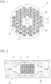
- the superconducting wire 10 in the present embodiment includes a core portion 11, a plurality of filaments 12 arranged on the outer peripheral side of the core portion 11, and an outer shell portion 13 arranged on the outer peripheral side of the plurality of the filaments 12.
- the filament 12 described above has a structure in which a strand 15 consisting of a superconducting material is surrounded with the stabilizer material for superconductor 20 in a state of being in electrical contact therewith. That is, the filament 12 includes the strand 15 and the stabilizer material for superconductor 20 which surrounds the strand 15 in a state of being in electrical contact with the strand 15.
- the strand 15 consisting of a superconducting material and the stabilizer material for superconductor 20 are in a state in which electricity can be conducted.
- the stabilizer material for superconductor 20 of the present embodiment includes a copper material, and the copper material contains one kind or two kinds or more of additive elements selected from Ca, La, and Ce for a total amount of 3 ppm by mass or more and 400 ppm by mass or less, with the remainder being Cu and unavoidable impurities, and the total concentration of the unavoidable impurities other than O, H, C, N, and S, which are gas components, is 5 ppm by mass or more and 100 ppm by mass or less (the stabilizer material for superconductor 20 consists of the copper material).
- compounds including one kind or two kinds or more selected from CaS, CaSO 4 , LaS, La 2 SO 2 , CeS, and Ce 2 SO 2 are present in the matrix. That is, one or more kinds selected from the above-described compounds are present in the matrix.
- a part of S may be substituted with Te or Se. Since the amounts of Te and Se are smaller than the amount of S, the amount of compounds consisting of either one of Te or Se with Ca, La, Ce, or the like is small, and compounds are formed in a state where a part of S in the compounds described above is substituted with Te or Se.
- the amount of Fe is 10 ppm by mass or less
- the amount of Ni is 10 ppm by mass or less
- the amount of As is 5 ppm by mass or less
- the amount of Ag is 50 ppm by mass or less
- the amount of Sn is 4 ppm by mass or less
- the amount of Sb is 4 ppm by mass or less
- the amount of Pb is 6 ppm by mass or less
- the amount of Bi is 2 ppm by mass or less
- the amount of P is 3 ppm by mass or less.
- a ratio Y/X of the total amount of one kind or two kinds or more of additive elements selected from Ca, La, and Ce (Y ppm by mass) to the total amount of S, Se, and Te (X ppm by mass) is in the range of 0.5 ⁇ Y/X ⁇ 100.
- the residual resistance ratio (RRR) is 250 or more.
- S, Se, and Te are elements which are dissolved in the copper that greatly decrease the residual resistance ratio (RRR). Therefore, in order to improve the residual resistance ratio (RRR), it is necessary to remove the influence of S, Se, and Te.
- One kind or two kinds or more of additive elements selected from Ca, La, and Ce are elements which are highly reactive with S, Se, and Te.
- the additive elements described above form compounds with S, Se, and Te; and thereby, it is possible to prevent S, Se, and Te from being dissolved in a copper. Due to this, it is possible to effectively improve the residual resistance ratio (RRR).
- RRR residual resistance ratio
- One kind or two kinds or more of additive elements selected from Ca, La, and Ce are elements which do not easily dissolve in copper and which have a small effect of decreasing the residual resistance ratio (RRR) even in the case when the additive elements dissolve in the copper. For this reason, the residual resistance ratio (RRR) does not decrease greatly even in the case when the additive elements described above are added in an excessive amount with respect to the amounts of S, Se, and Te.
- the total amount of one kind or two kinds or more of additive elements selected from Ca, La, and Ce is less than 3 ppm by mass, there is a concern that it will not be possible to effectively fix S, Se and Te.
- the total amount of one kind or two kinds or more of additive elements selected from Ca, La, and Ce exceeds 400 ppm by mass, there is a concern that coarse precipitates or the like of these additive elements will be produced, which deteriorates the workability. From the above-described reasons, in the present embodiment, the total amount of one kind or two kinds or more of additive elements selected from Ca, La, and Ce is defined to be within the range of 3 ppm by mass or more and 400 ppm by mass or less.
- the lower limit of the total amount of one kind or two kinds or more of additive elements selected from Ca, La, and Ce is preferably 3.5 ppm by mass or more, and more preferably 4.0 ppm by mass or more.
- the upper limit of the total amount of one kind or two kinds or more of additive elements selected from Ca, La, and Ce is preferably 300 ppm by mass or less, and more preferably 100 ppm by mass or less.
- the residual resistance ratio (RRR) is improved by lowering the concentrations of unavoidable impurities other than gas components (O, H, C, N, and S).
- the concentration of unavoidable impurities is to be reduced more than necessary, the production process becomes complex; and thereby, the production costs are drastically increased. Therefore, in the present embodiment, the total concentration of unavoidable impurities other than gas components (O, H, C, N, and S) is set to be in a range of 5 ppm by mass or more and 100 ppm by mass or less.
- the O concentration is preferably set to 20 ppm by mass or less, and the O concentration is more preferably 10 ppm by mass or less, and most preferably 5 ppm by mass or less.
- the lower limit of the unavoidable impurities other than (not including) O, H, C, N, and S, which are gas components is preferably set to 7 ppm by mass or more, and more preferably set to more than 10 ppm by mass.
- the total concentration of unavoidable impurities including O, H, C, N and S, which are gas components is preferably more than 10 ppm by mass, more preferably 15 ppm by mass or more, and most preferably 20 ppm by mass or more.
- the upper limit of the unavoidable impurities other than (not including) O, H, C, N and S, which are gas components is preferably 90 ppm by mass or less, and more preferably 80 ppm by mass or less.
- the unavoidable impurities other than gas components in the present embodiment are Fe, Ni, As, Ag, Sn, Sb, Pb, Bi, P, Li, Be, B, F, Na, Mg, Al, Si, Cl, K, Sc, Ti, V, Cr, Mn, Nb, Co, Zn, Ga, Ge, Br, Rb, Sr, Y, Zr, Mo, Ru, Pd, Cd, In, I, Cs, Ba, rare earth elements (other than La and Ce), Hf, Ta, W, Re, Os, Ir, Pt, Au, Hg, Tl, Th, and U.
- one kind or two kinds or more of additive elements selected from Ca, La, and Ce produce compounds with the elements such as S, Se, and Te so as to prevent the elements such as S, Se, and Te from being dissolved in the copper.
- compounds including compounds in which part of S is substituted with Te or Se
- compounds including one kind or two kinds or more selected from CaS, CaSO 4 , LaS, La 2 SO 2 , CeS, and Ce 2 SO 2
- RRR residual resistance ratio
- Compounds including one kind or two kinds or more selected from CaS, CaSO 4 , LaS, La 2 SO 2 , CeS, and Ce 2 SO 2 have high thermal stability and are able to be stably present even at high temperatures. These compounds are produced during the melting and casting process, but due to the characteristics described above, the compounds are stably present even after processing and after heat treatment. Therefore, even in the case when heat treatment is performed in a wide temperature range, S, Se, and Te are fixed as compounds, and it is possible to stably obtain a high residual resistance ratio (RRR).
- RRR residual resistance ratio
- the upper limit of the number density of the compounds (particle size of 0.1 ⁇ m or more) described above is 0.1 particles/ ⁇ m 2 or less, preferably 0.09 particles/ ⁇ m 2 or less, and more preferably 0.08 particles/ ⁇ m 2 or less.
- specific impurity elements such as Fe, Ni, As, Ag, Sn, Sb, Pb, Bi, and P have an effect of decreasing the residual resistance ratio (RRR). Therefore, the amount of each of these elements is defined; and thereby, it is possible to effectively prevent the decrease in the residual resistance ratio (RRR).
- the amount of Fe is set to 10 ppm by mass or less
- the amount of Ni is set to 10 ppm by mass or less
- the amount of As is set to 5 ppm by mass or less
- the amount of Ag is set to 50 ppm by mass or less
- the amount of Sn is set to 4 ppm by mass or less
- the amount of Sb is set to 4 ppm by mass or less
- the amount of Pb is set to 6 ppm by mass or less
- the amount of Bi is set to 2 ppm by mass or less
- the amount of P is set to 3 ppm by mass or less.
- the amount of Fe is preferably set to 4.5 ppm by mass or less
- the amount of Ni is preferably set to 3 ppm by mass or less
- the amount of As is preferably set to 3 ppm by mass or less
- the amount of Ag is preferably set to 38 ppm by mass or less
- the amount of Sn is preferably set to 3 ppm by mass or less
- the amount of Sb is preferably set to 1.5 ppm by mass or less
- the amount of Pb is preferably set to 4.5 ppm by mass or less
- the amount of Bi is preferably set to 1.5 ppm by mass or less
- the amount of P is preferably set to 1.5 ppm by mass or less.
- the amount of Fe is more preferably set to 3.3 ppm by mass or less, the amount of Ni is more preferably set to 2.2 ppm by mass or less, the amount of As is more preferably set to 2.2 ppm by mass or less, the amount of Ag is more preferably set to 28 ppm by mass or less, the amount of Sn is more preferably set to 2.2 ppm by mass or less, the amount of Sb is more preferably set to 1.1 ppm by mass or less, the amount of Pb is more preferably set to 3.3 ppm by mass or less, the amount of Bi is more preferably set to 1.1 ppm by mass or less, and the amount of P is more preferably set to 1.1 ppm by mass or less.
- the lower limits of the amounts of Fe, Ni, As, Ag, Sn, Sb, Pb, Bi, and P are 0 ppm by mass.
- the amount of Fe is preferably set to 0.1 ppm by mass or more
- the amount of Ni is preferably set to 0.1 ppm by mass or more
- the amount of As is preferably set to 0.1 ppm by mass or more
- the amount of Ag is preferably set to 0.1 ppm by mass or more
- the amount of Sn is preferably set to 0.1 ppm by mass or more
- the amount of Sb is preferably set to 0.1 ppm by mass or more
- the amount of Pb is preferably set to 0.1 ppm by mass or more
- the amount of Bi is preferably set to 0.1 ppm by mass or more
- the amount of P is preferably set to 0.1 ppm by mass or more.
- the lower limits are not limited thereto.
- one kind or two kinds or more of additive elements selected from Ca, La, and Ce form compounds with elements such as S, Se, and Te.
- the ratio Y/X of the total amount of the additive elements (Y ppm by mass) to the total amount of S, Se, and Te (X ppm by mass) is less than 0.5, the amount of the additive elements is insufficient, and there is a concern in that it may not be possible to effectively fix the elements such as S, Se, and Te.
- the ratio Y/X of the total amount (Y) of additive elements to the total amount (X) of S, Se, and Te is defined to be within the range of 0.5 or more and 100 or less.
- the lower limit of the ratio Y/X of the total amount of additive elements to the total amount of S, Se, and Te is preferably 0.75 or more, and more preferably 1.0 or more.
- the upper limit of the ratio Y/X of the total amount of additive elements to the total amount of S, Se, and Te is preferably 75 or less, and more preferably 50 or less.
- the lower limit of the total amount (X) of S, Se and Te in the stabilizer material for superconductor 20 is preferably more than 0 ppm by mass, more preferably 0.1 ppm by mass or more, even more preferably 0.5 ppm by mass or more, and most preferably 1 ppm by mass or more.
- the upper limit of the total amount (X) of S, Se and Te is preferably 25 ppm by mass or less, and more preferably 15 ppm by mass or less.
- the lower limit and the upper limit of the total amount (X) of S, Se and Te are not limited thereto.
- the residual resistance ratio (RRR) of the stabilizer material for superconductor 20 is 250 or more, the resistance value is low and it is possible to effectively bypass the current at extremely low temperatures.
- the residual resistance ratio (RRR) is preferably 280 or more, more preferably 300 or more.
- the residual resistance ratio (RRR) is even more preferably 400 or more.
- the upper limit of the residual resistance ratio (RRR) is preferably 10000 or less, more preferably 5000 or less, even more preferably 3000 or less, and 2000 or less is most preferable in order to effectively prevent increases in production costs; however, the residual resistance ratio (RRR) is not limited thereto.
- the stabilizer material for superconductor 20 of the present embodiment is produced by a process including a melting and casting step, a plastic working step, and a heat treatment step.
- a copper wire rod having the composition shown in the present embodiment may be produced by a continuous casting and rolling method (for example, the SCR method) or the like, and the stabilizer material for superconductor 20 of the present embodiment may be produced using this copper wire rod as a base material.
- the production efficiency of the stabilizer material for superconductor 20 of the present embodiment is improved, and it is possible to greatly reduce the production costs.
- the continuous casting and rolling method referred thereto is a step in which a copper wire rod is produced using a continuous casting and rolling facility including a belt-wheel type continuous casting apparatus and a continuous rolling device, and a drawn copper wire is produced using this copper wire rod as a base material.
- a copper is used in which the total concentration of unavoidable impurities other than O, H, C, N, and S, which are gas components, is 5 ppm by mass or more and 100 ppm by mass or less, it is not necessary to carry out excessively high purification of the copper, thus the production process is simple and it is possible to reduce the production costs.
- the stabilizer material for superconductor 20 of the present embodiment compounds including one kind or two kinds or more selected from CaS, CaSO 4 , LaS, La 2 SO 2 , CeS, and Ce 2 SO 2 are present in the matrix. For this reason, S, Se, and Te present in the copper are effectively fixed, and it is possible to improve the residual resistance ratio (RRR).
- RRR residual resistance ratio
- the compounds described above have high thermal stability, it is possible to stably obtain a high residual resistance ratio (RRR) even in the case when heat treatment is performed in a wide temperature range.
- the number density of the above-described compounds having a particle size of 0.1 ⁇ m or more is 0.001 particles/ ⁇ m 2 or more, it is possible to effectively fix S, Se, and Te as compounds, and it is possible to effectively improve the residual resistance ratio (RRR).
- the amounts of Fe, Ni, As, Ag, Sn, Sb, Pb, Bi, and P which influence the residual resistance ratio (RRR) are defined such that the amount of Fe is 10 ppm by mass or less, the amount of Ni is 10 ppm by mass or less, the amount of As is 5 ppm by mass or less, the amount of Ag is 50 ppm by mass or less, the amount of Sn is 4 ppm by mass or less, the amount of Sb is 4 ppm by mass or less, the amount of Pb is 6 ppm by mass or less, the amount of Bi is 2 ppm by mass or less, and the amount of P is 3 ppm by mass or less.
- RRR residual resistance ratio
- a ratio Y/X of the total amount of one kind or two kinds or more of additive elements selected from Ca, La, and Ce (Y ppm by mass) to the total amount of S, Se, and Te (X ppm by mass) is within the range of 0.5 ⁇ Y/X ⁇ 100. For this reason, it is possible to effectively fix S, Se, and Te in the copper as compounds with the additive elements, and it is possible to effectively prevent decreases in the residual resistance ratio (RRR). In addition, a large amount of excess additive elements which do not react with S, Se and Te are not present, and it is possible to preserve the workability.
- the resistance value at extremely low temperatures is sufficiently low.
- the superconducting wire 10 of the present embodiment includes the stabilizer material for superconductor 20 having a high residual resistance ratio (RRR) as described above, it is possible to effectively bypass the current to the stabilizer material for superconductor 20 even in the case when a normal conducting region A is generated in which the superconducting state is destroyed in the strand 15 consisting of a superconducting material, and the superconducting wire 10 can be stably used.
- RRR residual resistance ratio
- the superconducting coil of the present embodiment includes a winding frame and a winding portion, and the winding portion is a superconducting wire of the present embodiment wound around the peripheral surface of the winding frame.
- the present invention is not limited thereto and is able to be appropriately modified in the range of the technical features of the invention.
- the core portion 11 and the outer shell portion 13 that are included in the superconducting wire 10 may also consist of a copper material having the same composition as that of the stabilizer material for superconductor 20 of the present embodiment.
- the filaments 12 are arranged on the outer peripheral side of the core portion 11 in a state of being in electrical contact with the core portion 11.
- the outer shell portion 13 is arranged on the outer peripheral side of the filaments 12 in a state of being in electrical contact with the filaments 12.
- the core portion 11 and the stabilizer material for superconductor 20 of the filaments 12 contacting the core portion 11 may be integrated.
- the outer shell portion 13 and the stabilizer material for superconductor 20 of the filaments 12 contacting the outer shell portion 13 may be integrated.
- the core portion 11 and the outer shell portion 13 consist of a copper material having the same composition as that of the stabilizer material for superconductor 20 and the core portion 11 and the outer shell portion 13 are in a state of being in electrical contact with the filaments 12, the core portion 11 and the outer shell portion 13 function to exhibit the same actions as the stabilizer material for superconductor 20 in the filaments 12.
- the superconducting wire 10 having a structure in which a plurality of the filaments 12 are bundled is described as an example, but the present invention is not limited thereto.
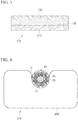
- a superconducting wire 110 having a structure in which a superconducting material 115 and a stabilizer material for superconductor 120 are laminated and arranged on a tape-like substrate 113 may be adopted. That is, the superconducting wire 110 may include the tape-like substrate 113, and the superconducting material 115 and the stabilizer material for superconductor 120 which are laminated on the substrate 113. The stabilizer material for superconductor 120 is laminated on the superconducting material 115 or surrounds the superconducting material 115 in a state of being in electrical contact with the superconducting material 115.
- the form (configuration) of the superconducting material 115 in FIG. 3 is a board (sheet, plate), but the form of the superconducting material 115 may be a strip, a wire, or a bar.
- a superconducting wire 210 having a structure in which a plurality of the filaments 12 are bundled and then assembled in a channel member 220 consisting of pure copper may be adopted. That is, the superconducting wire 210 may include a channel member 220 having a recess portion and a bundle of a plurality of the filaments 12 incorporated in the recess portion. The bundle of a plurality of the filaments 12 may be, for example, the superconducting wire 10 shown in FIG. 1 .
- high-purity copper was melted in an inert gas atmosphere of Ar using an electric furnace, then various base alloys of additive elements and impurities were added thereto and the concentration of the elements were adjusted to the predetermined values, and the resultant was casted into a predetermined mold to obtain an ingot having a diameter of 80 mm and a length of 120 mm.
- a square bar having cross-sectional dimensions of 20 mm ⁇ 20 mm was cut out and subjected to hot rolling at 825°C to obtain a hot-rolled wire rod having a diameter of 8 mm.
- the hot-rolled wire rod was subjected to cold drawing to form a fine wire having a diameter of 2.0 mm, and the fine wire was subjected to heat treatment for 1 hour at the temperature shown in Table 2 to produce a wire for evaluation.
- composition analysis was carried out as follows. For elements other than gas components, glow discharge mass spectrometry was used in the case where the amount was less than 10 ppm by mass, and inductively coupled plasma emission spectrometry was used in the case where the amount was 10 ppm by mass or more. In addition, infrared absorption method was used for analyzing the amount of S. All the measured O concentrations were 10 ppm by mass or less. The infrared absorption method was used for analyzing the amount of O.
- the average length of the major axis (the length of the longest straight line in a particle which does not come into contact with the particle edge) and the minor axis (the length of the longest straight line in the direction orthogonal to the major axis which does not come into contact with the particle edge) of the intermetallic compound was used.
- the compound having a particle size of 0.1 ⁇ m or more the composition was analyzed using the energy dispersive X-ray spectroscopy (EDX) method, and it was confirmed that the compound included Ca, La, Ce, and S.
- EDX energy dispersive X-ray spectroscopy
- the evaluation results are shown in Table 2.
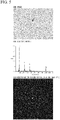
- the SEM observation result, the analysis result, and the electron diffraction result of the compound of Invention Example 3 are shown in FIG. 5
- the SEM observation result, the analysis result, and the electron diffraction result of the compound of Invention Example 10 are shown in FIG. 6 .
- Comparative Example 1 one kind or two or more of additive elements selected from Ca, La and Ce were not added, and, in the matrix, compounds including one kind or two kinds or more selected from CaS, CaSO 4 , LaS, La 2 SO 2 , CeS, and Ce 2 SO 2 were not present and the residual resistance ratio (RRR) was 141 which was low.
- RRR residual resistance ratio
- the stabilizer material for superconductor of the present invention is able to be produced with a relatively simple and inexpensive production process and has a sufficiently high residual resistance ratio (RRR). Therefore, it is possible to suitably apply the stabilizer material for superconductor of the present invention to superconducting wires and superconducting coils used in MRI, NMR, particle accelerators, maglev trains, power storage apparatuses, and the like.
- RRR residual resistance ratio
Landscapes
- Chemical & Material Sciences (AREA)
- Engineering & Computer Science (AREA)
- Mechanical Engineering (AREA)
- Organic Chemistry (AREA)
- Metallurgy (AREA)
- Materials Engineering (AREA)
- Crystallography & Structural Chemistry (AREA)
- Physics & Mathematics (AREA)
- Thermal Sciences (AREA)
- Power Engineering (AREA)
- Superconductors And Manufacturing Methods Therefor (AREA)
- Inorganic Compounds Of Heavy Metals (AREA)
- Windings For Motors And Generators (AREA)
- Compositions Of Oxide Ceramics (AREA)
Applications Claiming Priority (2)
| Application Number | Priority Date | Filing Date | Title |
|---|---|---|---|
| JP2016076899A JP6299802B2 (ja) | 2016-04-06 | 2016-04-06 | 超伝導安定化材、超伝導線及び超伝導コイル |
| PCT/JP2017/013924 WO2017175710A1 (ja) | 2016-04-06 | 2017-04-03 | 超伝導安定化材 |
Publications (3)
| Publication Number | Publication Date |
|---|---|
| EP3441484A1 true EP3441484A1 (de) | 2019-02-13 |
| EP3441484A4 EP3441484A4 (de) | 2019-09-18 |
| EP3441484B1 EP3441484B1 (de) | 2022-06-15 |
Family
ID=60000489
Family Applications (1)
| Application Number | Title | Priority Date | Filing Date |
|---|---|---|---|
| EP17779088.8A Active EP3441484B1 (de) | 2016-04-06 | 2017-04-03 | Stabilisatormaterial für supraleiter |
Country Status (7)
| Country | Link |
|---|---|
| US (1) | US11149329B2 (de) |
| EP (1) | EP3441484B1 (de) |
| JP (1) | JP6299802B2 (de) |
| KR (1) | KR102300408B1 (de) |
| CN (2) | CN112687789A (de) |
| TW (2) | TWI771296B (de) |
| WO (1) | WO2017175710A1 (de) |
Families Citing this family (2)
| Publication number | Priority date | Publication date | Assignee | Title |
|---|---|---|---|---|
| CN115011835A (zh) * | 2022-06-13 | 2022-09-06 | 上杭县紫金佳博电子新材料科技有限公司 | 一种镀银键合铜丝及其制备方法、应用 |
| CN118726791A (zh) * | 2024-07-18 | 2024-10-01 | 中国科学院金属研究所 | 一种高性能键合铜丝材料及其制备方法 |
Family Cites Families (45)
| Publication number | Priority date | Publication date | Assignee | Title |
|---|---|---|---|---|
| JPS5474698A (en) | 1977-11-28 | 1979-06-14 | Univ Tohoku | Superconductive thin band and method of fabricating same |
| JPS6058291B2 (ja) * | 1978-01-20 | 1985-12-19 | 住友電気工業株式会社 | 銅合金軟導体およびその製造法 |
| US4233067A (en) | 1978-01-19 | 1980-11-11 | Sumitomo Electric Industries, Ltd. | Soft copper alloy conductors |
| JPS6062009A (ja) * | 1983-09-14 | 1985-04-10 | 日立電線株式会社 | Ag入り無酸素銅により安定化された複合超電導体 |
| US4623862A (en) | 1984-12-27 | 1986-11-18 | Ga Technologies Inc. | Thermally stabilized superconductors |
| JPS6365036A (ja) | 1986-09-05 | 1988-03-23 | Furukawa Electric Co Ltd:The | 銅細線とその製造方法 |
| JPS63140052A (ja) | 1986-12-01 | 1988-06-11 | Hitachi Cable Ltd | 低温軟化性を有する無酸素銅ベ−ス希薄合金及びその用途 |
| JPS63235440A (ja) * | 1987-03-23 | 1988-09-30 | Furukawa Electric Co Ltd:The | 銅細線及びその製造方法 |
| JPH01143744A (ja) | 1987-11-30 | 1989-06-06 | Aichi Steel Works Ltd | 酸化物超電導細線の製造方法 |
| JPH02145737A (ja) | 1988-11-24 | 1990-06-05 | Dowa Mining Co Ltd | 高強度高導電性銅基合金 |
| JPH04224662A (ja) * | 1990-12-26 | 1992-08-13 | Hitachi Cable Ltd | 高残留抵抗比銅材の製造方法 |
| JP3047540B2 (ja) | 1991-07-23 | 2000-05-29 | 三菱マテリアル株式会社 | 高い残留抵抗比を有する超電導安定化材用高純度Cu合金 |
| CN1080779A (zh) * | 1993-05-05 | 1994-01-12 | 北京有色金属研究总院 | 极细多芯低温超导线带用的铜合金 |
| US6777331B2 (en) | 2000-03-07 | 2004-08-17 | Simplus Systems Corporation | Multilayered copper structure for improving adhesion property |
| US6745059B2 (en) | 2001-11-28 | 2004-06-01 | American Superconductor Corporation | Superconductor cables and magnetic devices |
| JP3851593B2 (ja) | 2002-07-02 | 2006-11-29 | 株式会社神戸製鋼所 | Nb3Sn系超電導線材用ブロンズ材およびこれを用いた超電導線材用複合材、並びに超電導線材 |
| US20040266628A1 (en) | 2003-06-27 | 2004-12-30 | Superpower, Inc. | Novel superconducting articles, and methods for forming and using same |
| US7774035B2 (en) | 2003-06-27 | 2010-08-10 | Superpower, Inc. | Superconducting articles having dual sided structures |
| JP2005056754A (ja) | 2003-08-06 | 2005-03-03 | Sumitomo Electric Ind Ltd | 超電導線材およびその製造方法 |
| US8192596B2 (en) | 2004-01-29 | 2012-06-05 | Jx Nippon Mining & Metals Corporation | Ultrahigh-purity copper and process for producing the same |
| AT7491U1 (de) | 2004-07-15 | 2005-04-25 | Plansee Ag | Werkstoff für leitbahnen aus kupferlegierung |
| KR101006035B1 (ko) | 2005-06-15 | 2011-01-06 | 제이엑스 닛코 닛세키 킨조쿠 가부시키가이샤 | 초고순도 구리 및 그 제조 방법 그리고 초고순도 구리로이루어지는 본딩 와이어 |
| JP2009507358A (ja) | 2005-07-29 | 2009-02-19 | アメリカン・スーパーコンダクター・コーポレーション | 高温超電導ワイヤ及びコイル |
| WO2007136406A2 (en) * | 2005-11-08 | 2007-11-29 | Supramagnetics, Inc. | Composite conductors with improved structural and electrical properties |
| JP4538813B2 (ja) | 2006-05-29 | 2010-09-08 | Dowaホールディングス株式会社 | 銅基合金材を用いたコネクタ及び充電用ソケット |
| JP5402518B2 (ja) | 2009-10-20 | 2014-01-29 | 住友電気工業株式会社 | 酸化物超電導コイル、酸化物超電導コイル体および回転機 |
| JP5717236B2 (ja) | 2010-05-12 | 2015-05-13 | 三菱マテリアル株式会社 | 粒子加速器 |
| JP5589753B2 (ja) * | 2010-10-20 | 2014-09-17 | 日立金属株式会社 | 溶接部材、及びその製造方法 |
| CN102568694A (zh) * | 2010-12-23 | 2012-07-11 | 吴仕驹 | 高温超导体及其制备方法 |
| PH12014500149A1 (en) | 2011-07-22 | 2017-05-19 | Mitsubishi Materials Corp | Copper strand for bonding wire and method for producing copper strand for bonding wire |
| TWI571518B (zh) * | 2011-08-29 | 2017-02-21 | Furukawa Electric Co Ltd | Copper alloy material and manufacturing method thereof |
| JP2013049893A (ja) | 2011-08-31 | 2013-03-14 | Mitsubishi Materials Corp | 太陽電池インターコネクタ用導体及び太陽電池用インターコネクタ |
| SG190482A1 (en) * | 2011-12-01 | 2013-06-28 | Heraeus Materials Tech Gmbh | Doped 4n copper wire for bonding in microelectronics device |
| EP2808419B1 (de) * | 2012-01-23 | 2016-08-31 | JX Nippon Mining & Metals Corporation | Hochreines kupfer-mangan-legierungs-sputtertarget |
| DE102012205843A1 (de) | 2012-04-11 | 2013-10-17 | Bruker Eas Gmbh | NbTi-Supraleiter mit reduziertem Gewicht |
| TWI403596B (zh) | 2012-10-29 | 2013-08-01 | 呂傳盛 | 半導體封裝用之銅合金線 |
| JP6101491B2 (ja) | 2012-11-30 | 2017-03-22 | 株式会社フジクラ | 酸化物超電導線材及びその製造方法 |
| JP5752736B2 (ja) * | 2013-04-08 | 2015-07-22 | 三菱マテリアル株式会社 | スパッタリング用ターゲット |
| JP5962707B2 (ja) | 2013-07-31 | 2016-08-03 | 三菱マテリアル株式会社 | 電子・電気機器用銅合金、電子・電気機器用銅合金塑性加工材、電子・電気機器用銅合金塑性加工材の製造方法、電子・電気機器用部品及び端子 |
| JP5866411B2 (ja) | 2013-08-09 | 2016-02-17 | 三菱マテリアル株式会社 | 銅合金薄板および銅合金薄板の製造方法 |
| JP6311299B2 (ja) * | 2013-12-11 | 2018-04-18 | 三菱マテリアル株式会社 | 電子・電気機器用銅合金、電子・電気機器用銅合金塑性加工材、電子・電気機器用銅合金塑性加工材の製造方法、電子・電気機器用部品及び端子 |
| CN103985479B (zh) | 2014-04-28 | 2018-03-30 | 赵遵成 | 一种高温超导涂层导体带材的制备方法 |
| JP6056877B2 (ja) * | 2015-01-07 | 2017-01-11 | 三菱マテリアル株式会社 | 超伝導線、及び、超伝導コイル |
| JP6056876B2 (ja) * | 2015-01-07 | 2017-01-11 | 三菱マテリアル株式会社 | 超伝導安定化材 |
| JP6299803B2 (ja) * | 2016-04-06 | 2018-03-28 | 三菱マテリアル株式会社 | 超伝導線、及び、超伝導コイル |
-
2016
- 2016-04-06 JP JP2016076899A patent/JP6299802B2/ja active Active
-
2017
- 2017-04-03 CN CN202011441833.3A patent/CN112687789A/zh active Pending
- 2017-04-03 KR KR1020187025123A patent/KR102300408B1/ko active Active
- 2017-04-03 WO PCT/JP2017/013924 patent/WO2017175710A1/ja not_active Ceased
- 2017-04-03 CN CN201780008657.4A patent/CN108603250B/zh active Active
- 2017-04-03 US US16/090,788 patent/US11149329B2/en active Active
- 2017-04-03 EP EP17779088.8A patent/EP3441484B1/de active Active
- 2017-04-05 TW TW106111410A patent/TWI771296B/zh active
- 2017-04-05 TW TW111121876A patent/TWI812277B/zh active
Also Published As
| Publication number | Publication date |
|---|---|
| JP6299802B2 (ja) | 2018-03-28 |
| CN108603250A (zh) | 2018-09-28 |
| TW202242154A (zh) | 2022-11-01 |
| TW201807205A (zh) | 2018-03-01 |
| JP2017186621A (ja) | 2017-10-12 |
| KR102300408B1 (ko) | 2021-09-08 |
| CN108603250B (zh) | 2020-12-18 |
| US20190338396A1 (en) | 2019-11-07 |
| TWI812277B (zh) | 2023-08-11 |
| KR20180131536A (ko) | 2018-12-10 |
| WO2017175710A1 (ja) | 2017-10-12 |
| CN112687789A (zh) | 2021-04-20 |
| EP3441484A4 (de) | 2019-09-18 |
| TWI771296B (zh) | 2022-07-21 |
| US11149329B2 (en) | 2021-10-19 |
| EP3441484B1 (de) | 2022-06-15 |
Similar Documents
| Publication | Publication Date | Title |
|---|---|---|
| EP3441486B1 (de) | Supraleitender draht und supraleitende spule | |
| EP3441485B1 (de) | Stabilisatormaterial für supraleiter, supraleitenden draht und supraleitende spule | |
| US20210225560A1 (en) | Superconducting wire and superconducting coil | |
| EP3243917B1 (de) | Supraleitendes stabilisatormaterial, supraleitender draht und supraleitende spule | |
| EP3441484B1 (de) | Stabilisatormaterial für supraleiter | |
| EP3705589B1 (de) | Supraleitendes stabilisierungsmaterial, supraleitender draht und supraleitende spule | |
| JP6057008B2 (ja) | 超伝導線、及び、超伝導コイル |
Legal Events
| Date | Code | Title | Description |
|---|---|---|---|
| STAA | Information on the status of an ep patent application or granted ep patent |
Free format text: STATUS: THE INTERNATIONAL PUBLICATION HAS BEEN MADE |
|
| PUAI | Public reference made under article 153(3) epc to a published international application that has entered the european phase |
Free format text: ORIGINAL CODE: 0009012 |
|
| STAA | Information on the status of an ep patent application or granted ep patent |
Free format text: STATUS: REQUEST FOR EXAMINATION WAS MADE |
|
| 17P | Request for examination filed |
Effective date: 20181011 |
|
| AK | Designated contracting states |
Kind code of ref document: A1 Designated state(s): AL AT BE BG CH CY CZ DE DK EE ES FI FR GB GR HR HU IE IS IT LI LT LU LV MC MK MT NL NO PL PT RO RS SE SI SK SM TR |
|
| AX | Request for extension of the european patent |
Extension state: BA ME |
|
| DAV | Request for validation of the european patent (deleted) | ||
| DAX | Request for extension of the european patent (deleted) | ||
| RAP1 | Party data changed (applicant data changed or rights of an application transferred) |
Owner name: MITSUBISHI MATERIALS CORPORATION |
|
| A4 | Supplementary search report drawn up and despatched |
Effective date: 20190821 |
|
| RIC1 | Information provided on ipc code assigned before grant |
Ipc: C22F 1/08 20060101ALI20190814BHEP Ipc: C22C 9/00 20060101AFI20190814BHEP Ipc: H02K 3/02 20060101ALI20190814BHEP Ipc: C22F 1/00 20060101ALI20190814BHEP Ipc: H01F 6/06 20060101ALI20190814BHEP |
|
| STAA | Information on the status of an ep patent application or granted ep patent |
Free format text: STATUS: EXAMINATION IS IN PROGRESS |
|
| 17Q | First examination report despatched |
Effective date: 20200706 |
|
| GRAP | Despatch of communication of intention to grant a patent |
Free format text: ORIGINAL CODE: EPIDOSNIGR1 |
|
| STAA | Information on the status of an ep patent application or granted ep patent |
Free format text: STATUS: GRANT OF PATENT IS INTENDED |
|
| INTG | Intention to grant announced |
Effective date: 20220215 |
|
| GRAS | Grant fee paid |
Free format text: ORIGINAL CODE: EPIDOSNIGR3 |
|
| GRAA | (expected) grant |
Free format text: ORIGINAL CODE: 0009210 |
|
| STAA | Information on the status of an ep patent application or granted ep patent |
Free format text: STATUS: THE PATENT HAS BEEN GRANTED |
|
| AK | Designated contracting states |
Kind code of ref document: B1 Designated state(s): AL AT BE BG CH CY CZ DE DK EE ES FI FR GB GR HR HU IE IS IT LI LT LU LV MC MK MT NL NO PL PT RO RS SE SI SK SM TR |
|
| REG | Reference to a national code |
Ref country code: CH Ref legal event code: EP Ref country code: GB Ref legal event code: FG4D |
|
| REG | Reference to a national code |
Ref country code: FI Ref legal event code: FGE Ref country code: IE Ref legal event code: FG4D |
|
| REG | Reference to a national code |
Ref country code: DE Ref legal event code: R096 Ref document number: 602017058543 Country of ref document: DE |
|
| REG | Reference to a national code |
Ref country code: AT Ref legal event code: REF Ref document number: 1498451 Country of ref document: AT Kind code of ref document: T Effective date: 20220715 |
|
| REG | Reference to a national code |
Ref country code: LT Ref legal event code: MG9D |
|
| REG | Reference to a national code |
Ref country code: NL Ref legal event code: MP Effective date: 20220615 |
|
| PG25 | Lapsed in a contracting state [announced via postgrant information from national office to epo] |
Ref country code: SE Free format text: LAPSE BECAUSE OF FAILURE TO SUBMIT A TRANSLATION OF THE DESCRIPTION OR TO PAY THE FEE WITHIN THE PRESCRIBED TIME-LIMIT Effective date: 20220615 Ref country code: NO Free format text: LAPSE BECAUSE OF FAILURE TO SUBMIT A TRANSLATION OF THE DESCRIPTION OR TO PAY THE FEE WITHIN THE PRESCRIBED TIME-LIMIT Effective date: 20220915 Ref country code: LT Free format text: LAPSE BECAUSE OF FAILURE TO SUBMIT A TRANSLATION OF THE DESCRIPTION OR TO PAY THE FEE WITHIN THE PRESCRIBED TIME-LIMIT Effective date: 20220615 Ref country code: HR Free format text: LAPSE BECAUSE OF FAILURE TO SUBMIT A TRANSLATION OF THE DESCRIPTION OR TO PAY THE FEE WITHIN THE PRESCRIBED TIME-LIMIT Effective date: 20220615 Ref country code: GR Free format text: LAPSE BECAUSE OF FAILURE TO SUBMIT A TRANSLATION OF THE DESCRIPTION OR TO PAY THE FEE WITHIN THE PRESCRIBED TIME-LIMIT Effective date: 20220916 Ref country code: BG Free format text: LAPSE BECAUSE OF FAILURE TO SUBMIT A TRANSLATION OF THE DESCRIPTION OR TO PAY THE FEE WITHIN THE PRESCRIBED TIME-LIMIT Effective date: 20220915 |
|
| REG | Reference to a national code |
Ref country code: AT Ref legal event code: MK05 Ref document number: 1498451 Country of ref document: AT Kind code of ref document: T Effective date: 20220615 |
|
| PG25 | Lapsed in a contracting state [announced via postgrant information from national office to epo] |
Ref country code: RS Free format text: LAPSE BECAUSE OF FAILURE TO SUBMIT A TRANSLATION OF THE DESCRIPTION OR TO PAY THE FEE WITHIN THE PRESCRIBED TIME-LIMIT Effective date: 20220615 Ref country code: LV Free format text: LAPSE BECAUSE OF FAILURE TO SUBMIT A TRANSLATION OF THE DESCRIPTION OR TO PAY THE FEE WITHIN THE PRESCRIBED TIME-LIMIT Effective date: 20220615 |
|
| PG25 | Lapsed in a contracting state [announced via postgrant information from national office to epo] |
Ref country code: NL Free format text: LAPSE BECAUSE OF FAILURE TO SUBMIT A TRANSLATION OF THE DESCRIPTION OR TO PAY THE FEE WITHIN THE PRESCRIBED TIME-LIMIT Effective date: 20220615 |
|
| PG25 | Lapsed in a contracting state [announced via postgrant information from national office to epo] |
Ref country code: SM Free format text: LAPSE BECAUSE OF FAILURE TO SUBMIT A TRANSLATION OF THE DESCRIPTION OR TO PAY THE FEE WITHIN THE PRESCRIBED TIME-LIMIT Effective date: 20220615 Ref country code: SK Free format text: LAPSE BECAUSE OF FAILURE TO SUBMIT A TRANSLATION OF THE DESCRIPTION OR TO PAY THE FEE WITHIN THE PRESCRIBED TIME-LIMIT Effective date: 20220615 Ref country code: RO Free format text: LAPSE BECAUSE OF FAILURE TO SUBMIT A TRANSLATION OF THE DESCRIPTION OR TO PAY THE FEE WITHIN THE PRESCRIBED TIME-LIMIT Effective date: 20220615 Ref country code: PT Free format text: LAPSE BECAUSE OF FAILURE TO SUBMIT A TRANSLATION OF THE DESCRIPTION OR TO PAY THE FEE WITHIN THE PRESCRIBED TIME-LIMIT Effective date: 20221017 Ref country code: ES Free format text: LAPSE BECAUSE OF FAILURE TO SUBMIT A TRANSLATION OF THE DESCRIPTION OR TO PAY THE FEE WITHIN THE PRESCRIBED TIME-LIMIT Effective date: 20220615 Ref country code: EE Free format text: LAPSE BECAUSE OF FAILURE TO SUBMIT A TRANSLATION OF THE DESCRIPTION OR TO PAY THE FEE WITHIN THE PRESCRIBED TIME-LIMIT Effective date: 20220615 Ref country code: CZ Free format text: LAPSE BECAUSE OF FAILURE TO SUBMIT A TRANSLATION OF THE DESCRIPTION OR TO PAY THE FEE WITHIN THE PRESCRIBED TIME-LIMIT Effective date: 20220615 Ref country code: AT Free format text: LAPSE BECAUSE OF FAILURE TO SUBMIT A TRANSLATION OF THE DESCRIPTION OR TO PAY THE FEE WITHIN THE PRESCRIBED TIME-LIMIT Effective date: 20220615 |
|
| PG25 | Lapsed in a contracting state [announced via postgrant information from national office to epo] |
Ref country code: PL Free format text: LAPSE BECAUSE OF FAILURE TO SUBMIT A TRANSLATION OF THE DESCRIPTION OR TO PAY THE FEE WITHIN THE PRESCRIBED TIME-LIMIT Effective date: 20220615 Ref country code: IS Free format text: LAPSE BECAUSE OF FAILURE TO SUBMIT A TRANSLATION OF THE DESCRIPTION OR TO PAY THE FEE WITHIN THE PRESCRIBED TIME-LIMIT Effective date: 20221015 |
|
| REG | Reference to a national code |
Ref country code: DE Ref legal event code: R097 Ref document number: 602017058543 Country of ref document: DE |
|
| PG25 | Lapsed in a contracting state [announced via postgrant information from national office to epo] |
Ref country code: AL Free format text: LAPSE BECAUSE OF FAILURE TO SUBMIT A TRANSLATION OF THE DESCRIPTION OR TO PAY THE FEE WITHIN THE PRESCRIBED TIME-LIMIT Effective date: 20220615 |
|
| PLBE | No opposition filed within time limit |
Free format text: ORIGINAL CODE: 0009261 |
|
| STAA | Information on the status of an ep patent application or granted ep patent |
Free format text: STATUS: NO OPPOSITION FILED WITHIN TIME LIMIT |
|
| PG25 | Lapsed in a contracting state [announced via postgrant information from national office to epo] |
Ref country code: DK Free format text: LAPSE BECAUSE OF FAILURE TO SUBMIT A TRANSLATION OF THE DESCRIPTION OR TO PAY THE FEE WITHIN THE PRESCRIBED TIME-LIMIT Effective date: 20220615 |
|
| 26N | No opposition filed |
Effective date: 20230316 |
|
| PG25 | Lapsed in a contracting state [announced via postgrant information from national office to epo] |
Ref country code: SI Free format text: LAPSE BECAUSE OF FAILURE TO SUBMIT A TRANSLATION OF THE DESCRIPTION OR TO PAY THE FEE WITHIN THE PRESCRIBED TIME-LIMIT Effective date: 20220615 |
|
| REG | Reference to a national code |
Ref country code: CH Ref legal event code: PL |
|
| PG25 | Lapsed in a contracting state [announced via postgrant information from national office to epo] |
Ref country code: LU Free format text: LAPSE BECAUSE OF NON-PAYMENT OF DUE FEES Effective date: 20230403 |
|
| REG | Reference to a national code |
Ref country code: BE Ref legal event code: MM Effective date: 20230430 |
|
| PG25 | Lapsed in a contracting state [announced via postgrant information from national office to epo] |
Ref country code: MC Free format text: LAPSE BECAUSE OF FAILURE TO SUBMIT A TRANSLATION OF THE DESCRIPTION OR TO PAY THE FEE WITHIN THE PRESCRIBED TIME-LIMIT Effective date: 20220615 |
|
| PG25 | Lapsed in a contracting state [announced via postgrant information from national office to epo] |
Ref country code: MC Free format text: LAPSE BECAUSE OF FAILURE TO SUBMIT A TRANSLATION OF THE DESCRIPTION OR TO PAY THE FEE WITHIN THE PRESCRIBED TIME-LIMIT Effective date: 20220615 Ref country code: LI Free format text: LAPSE BECAUSE OF NON-PAYMENT OF DUE FEES Effective date: 20230430 Ref country code: IT Free format text: LAPSE BECAUSE OF FAILURE TO SUBMIT A TRANSLATION OF THE DESCRIPTION OR TO PAY THE FEE WITHIN THE PRESCRIBED TIME-LIMIT Effective date: 20220615 Ref country code: CH Free format text: LAPSE BECAUSE OF NON-PAYMENT OF DUE FEES Effective date: 20230430 |
|
| REG | Reference to a national code |
Ref country code: IE Ref legal event code: MM4A |
|
| PG25 | Lapsed in a contracting state [announced via postgrant information from national office to epo] |
Ref country code: BE Free format text: LAPSE BECAUSE OF NON-PAYMENT OF DUE FEES Effective date: 20230430 |
|
| PG25 | Lapsed in a contracting state [announced via postgrant information from national office to epo] |
Ref country code: IE Free format text: LAPSE BECAUSE OF NON-PAYMENT OF DUE FEES Effective date: 20230403 |
|
| PG25 | Lapsed in a contracting state [announced via postgrant information from national office to epo] |
Ref country code: IE Free format text: LAPSE BECAUSE OF NON-PAYMENT OF DUE FEES Effective date: 20230403 |
|
| PG25 | Lapsed in a contracting state [announced via postgrant information from national office to epo] |
Ref country code: BG Free format text: LAPSE BECAUSE OF FAILURE TO SUBMIT A TRANSLATION OF THE DESCRIPTION OR TO PAY THE FEE WITHIN THE PRESCRIBED TIME-LIMIT Effective date: 20220615 |
|
| PG25 | Lapsed in a contracting state [announced via postgrant information from national office to epo] |
Ref country code: BG Free format text: LAPSE BECAUSE OF FAILURE TO SUBMIT A TRANSLATION OF THE DESCRIPTION OR TO PAY THE FEE WITHIN THE PRESCRIBED TIME-LIMIT Effective date: 20220615 |
|
| PGFP | Annual fee paid to national office [announced via postgrant information from national office to epo] |
Ref country code: FI Payment date: 20250424 Year of fee payment: 9 |
|
| PGFP | Annual fee paid to national office [announced via postgrant information from national office to epo] |
Ref country code: DE Payment date: 20250422 Year of fee payment: 9 |
|
| PGFP | Annual fee paid to national office [announced via postgrant information from national office to epo] |
Ref country code: GB Payment date: 20250423 Year of fee payment: 9 |
|
| PGFP | Annual fee paid to national office [announced via postgrant information from national office to epo] |
Ref country code: FR Payment date: 20250425 Year of fee payment: 9 |
|
| PG25 | Lapsed in a contracting state [announced via postgrant information from national office to epo] |
Ref country code: CY Free format text: LAPSE BECAUSE OF FAILURE TO SUBMIT A TRANSLATION OF THE DESCRIPTION OR TO PAY THE FEE WITHIN THE PRESCRIBED TIME-LIMIT; INVALID AB INITIO Effective date: 20170403 |
|
| PG25 | Lapsed in a contracting state [announced via postgrant information from national office to epo] |
Ref country code: HU Free format text: LAPSE BECAUSE OF FAILURE TO SUBMIT A TRANSLATION OF THE DESCRIPTION OR TO PAY THE FEE WITHIN THE PRESCRIBED TIME-LIMIT; INVALID AB INITIO Effective date: 20170403 |
|
| PG25 | Lapsed in a contracting state [announced via postgrant information from national office to epo] |
Ref country code: TR Free format text: LAPSE BECAUSE OF FAILURE TO SUBMIT A TRANSLATION OF THE DESCRIPTION OR TO PAY THE FEE WITHIN THE PRESCRIBED TIME-LIMIT Effective date: 20220615 |