EP3435427A1 - Light emitting devices with compact active regions - Google Patents
Light emitting devices with compact active regions Download PDFInfo
- Publication number
- EP3435427A1 EP3435427A1 EP18188922.1A EP18188922A EP3435427A1 EP 3435427 A1 EP3435427 A1 EP 3435427A1 EP 18188922 A EP18188922 A EP 18188922A EP 3435427 A1 EP3435427 A1 EP 3435427A1
- Authority
- EP
- European Patent Office
- Prior art keywords
- active region
- region
- light
- light emitting
- contact
- Prior art date
- Legal status (The legal status is an assumption and is not a legal conclusion. Google has not performed a legal analysis and makes no representation as to the accuracy of the status listed.)
- Ceased
Links
Images


Classifications
-
- H—ELECTRICITY
- H10—SEMICONDUCTOR DEVICES; ELECTRIC SOLID-STATE DEVICES NOT OTHERWISE PROVIDED FOR
- H10H—INORGANIC LIGHT-EMITTING SEMICONDUCTOR DEVICES HAVING POTENTIAL BARRIERS
- H10H20/00—Individual inorganic light-emitting semiconductor devices having potential barriers, e.g. light-emitting diodes [LED]
- H10H20/80—Constructional details
- H10H20/81—Bodies
- H10H20/814—Bodies having reflecting means, e.g. semiconductor Bragg reflectors
-
- H—ELECTRICITY
- H10—SEMICONDUCTOR DEVICES; ELECTRIC SOLID-STATE DEVICES NOT OTHERWISE PROVIDED FOR
- H10H—INORGANIC LIGHT-EMITTING SEMICONDUCTOR DEVICES HAVING POTENTIAL BARRIERS
- H10H20/00—Individual inorganic light-emitting semiconductor devices having potential barriers, e.g. light-emitting diodes [LED]
- H10H20/80—Constructional details
- H10H20/81—Bodies
- H10H20/819—Bodies characterised by their shape, e.g. curved or truncated substrates
-
- H—ELECTRICITY
- H10—SEMICONDUCTOR DEVICES; ELECTRIC SOLID-STATE DEVICES NOT OTHERWISE PROVIDED FOR
- H10H—INORGANIC LIGHT-EMITTING SEMICONDUCTOR DEVICES HAVING POTENTIAL BARRIERS
- H10H20/00—Individual inorganic light-emitting semiconductor devices having potential barriers, e.g. light-emitting diodes [LED]
- H10H20/80—Constructional details
- H10H20/83—Electrodes
- H10H20/832—Electrodes characterised by their material
- H10H20/835—Reflective materials
-
- H—ELECTRICITY
- H10—SEMICONDUCTOR DEVICES; ELECTRIC SOLID-STATE DEVICES NOT OTHERWISE PROVIDED FOR
- H10K—ORGANIC ELECTRIC SOLID-STATE DEVICES
- H10K50/00—Organic light-emitting devices
- H10K50/80—Constructional details
- H10K50/85—Arrangements for extracting light from the devices
- H10K50/852—Arrangements for extracting light from the devices comprising a resonant cavity structure, e.g. Bragg reflector pair
-
- H—ELECTRICITY
- H10—SEMICONDUCTOR DEVICES; ELECTRIC SOLID-STATE DEVICES NOT OTHERWISE PROVIDED FOR
- H10W—GENERIC PACKAGES, INTERCONNECTIONS, CONNECTORS OR OTHER CONSTRUCTIONAL DETAILS OF DEVICES COVERED BY CLASS H10
- H10W72/00—Interconnections or connectors in packages
- H10W72/20—Bump connectors, e.g. solder bumps or copper pillars; Dummy bumps; Thermal bumps
- H10W72/221—Structures or relative sizes
- H10W72/227—Multiple bumps having different sizes
-
- H—ELECTRICITY
- H10—SEMICONDUCTOR DEVICES; ELECTRIC SOLID-STATE DEVICES NOT OTHERWISE PROVIDED FOR
- H10W—GENERIC PACKAGES, INTERCONNECTIONS, CONNECTORS OR OTHER CONSTRUCTIONAL DETAILS OF DEVICES COVERED BY CLASS H10
- H10W90/00—Package configurations
- H10W90/701—Package configurations characterised by the relative positions of pads or connectors relative to package parts
- H10W90/721—Package configurations characterised by the relative positions of pads or connectors relative to package parts of bump connectors
- H10W90/724—Package configurations characterised by the relative positions of pads or connectors relative to package parts of bump connectors between a chip and a stacked insulating package substrate, interposer or RDL
Definitions
- the invention is related to light emitting devices with reflective contacts.
- LEDs light emitting diodes
- III-V semiconductors particularly binary, ternary, and quaternary alloys of gallium, aluminum, indium, and nitrogen, also referred to as III-nitride materials; and binary, ternary, and quaternary alloys of gallium, aluminum, indium, and phosphorus, also referred to as III-phosphide materials.
- III-nitride devices are epitaxially grown on sapphire, silicon carbide, or III-nitride substrates and III-phosphide devices are epitaxially grown on gallium arsenide by metal organic chemical vapor deposition (MOCVD) molecular beam epitaxy (MBE) or other epitaxial techniques.
- MOCVD metal organic chemical vapor deposition
- MBE molecular beam epitaxy
- an n-type layer (or layers) is deposited on the substrate, then an active region is deposited on the n-type layers, then a p-type layer (or layers) is deposited on the active region. The order of the layers may be reversed such that the p-type layers are adjacent to the substrate. Needed in the art are LED structures that increase the amount of light extracted from the device.
- a light emitting device includes a region of first conductivity type, a region of second conductivity type, an active region, and an electrode.
- the active region is disposed between the region of first conductivity type and the region of second conductivity type and the region of second conductivity type is disposed between the active region and the electrode.
- the active region includes a plurality of clusters, with a portion of a first cluster located between about 0.6 ⁇ n and 0.75 ⁇ n from the electrode and a portion of a second cluster located between about 1.2 ⁇ n and 1.35 ⁇ n from the electrode.
- Embodiments of the invention are directed to semiconductor light emitting devices. Embodiments of the invention may be applicable to organic light emitting devices, or any other suitable flip chip device.
- Fig. 1 illustrates a light emitting device according to embodiments of the present invention.
- a group of semiconductor layers including an n-type region 3, a light emitting active region 1, and a p-type region 5 are formed over a substrate 2.
- the semiconductor layers may be, for example, III-nitride layers, III-phosphide layers, II-VI layers, or any other suitable material.
- Each of n-type region 3, active region 1, and p-type region 5 may include multiple layers of the same or different composition, thickness, and dopant concentration.
- a portion of p-type region 5 and active region 1 are removed to expose a portion of n-type region 3.
- n-electrode 10 is deposited on n-type region 3 and a p-electrode 4 is deposited on p-type region 5. At least one of the p- and n-electrodes are highly reflective of light emitted by active region 1.
- the device is physically mounted on and electrically connected to a submount 9 by interconnects 8.
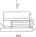
- Fig. 8 illustrates an alternative embodiment of a semiconductor light emitting device.
- p-type region 5 is separated from p-electrode 4 by a reflective surface 50 such as a distributed Bragg reflector (DBR).
- DBR distributed Bragg reflector
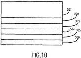
- Fig. 10 illustrates a thin film luminescent device such as an organic light emitting diode, according to embodiments of the present invention.
- a phosphor light emitting layer 304 is sandwiched between two insulators 303 and 305. Contact is made to the device through metal layer 306 and transparent electrode 302. Light is extracted through a glass superstrate 301.
- Organic light emitting diodes are described in more detail in Kristiaan Neyts, "Microcavities for Electroluminescent Devices," Chapter 4, Electroluminescence II, ed. Gerd Mueller, Semiconductors and Semimetals, Vol. 65 .
- Light extraction efficiency may be improved by controlling the placement of the light emitting layers relative to reflective layers in the device.
- the placement of active region 1 is controlled relative to the highly reflective p-electrode 4.
- the placement of active region 1 is controlled relative to DBR 50.
- the placement of phosphor layer 304 is controlled relative to metal layer 306.
- slight detuning of the resonance condition by moving the active region slightly closer to (or farther from) the p-electrode reflector, may be preferred to optimize the emission of light into the escape cone, and thus the total top surface extraction from the chip.
- the distance between the active region and a perfectly conducting metal p-electrode should be approximately one quarter-wavelength.
- the total amount of light emitted from the LED is the integrated flux emitted from the topside (towards the substrate) of the device added to the integrated flux emitted from the sides of the device.
- Side-emitted light is typically guided to the sides of the device by a waveguide created by reflective surfaces and various device layers having different indices of refraction. Waveguided light typically undergoes several reflections on its path to the side of the device, losing intensity with each reflection. In addition, light passing through the active region may be absorbed. Thus it is advantageous to extract as much light as possible from the topside of the device in the first pass, tending thereby to reduce internal losses and increase the total integrated flux.
- Flipchip LEDs have a "top escape cone" near the active region such that light impinging on the topside from within the LED and lying within the escape cone exit directly from the topside of the device.
- the top escape cone merely as the "escape cone,” understanding thereby that maximum topside light emission is a significant LED performance goal.
- the escape cone is determined by several device parameters including the indices of refraction of the various layers within the device, according to Snell's law. Light beams impinging on the topside outside the escape cone undergo total internal reflection. Such internally reflected light typically exits from the side of the device or undergoes further internal reflections and loss of intensity within the device.
- one approach to increasing the intensity emerging from the topside of the LED is to increase the flux impinging on the topside that lies within the escape cone.
- Fig. 2 depicts light escaping from a portion of the device illustrated in Fig. 1 .
- the reflective positive ohmic contact 4 lies at a separation d from active region 1 and has p-type region 5 lying between the active region 1 and the contact 4.
- Region 5 can comprise one layer or can comprise multiple sublayers having distinct compositions, doping characteristics and refractive indices from sublayer to sublayer or a gradation of compositions, electrical properties and optical properties throughout the thickness of p-type region 5.
- refraction away from the normal occurs as depicted in Fig. 2 , causing light 8 to emerge from substrate 2 into encapsulating gel 7 with an angle from the normal of ⁇ 3 .
- sapphire and encapsulating gel yields ⁇ 1 (escape) ⁇ 38.7°.
- ⁇ 1 (escape) ⁇ 38.7°.
- Light emitted from electron-hole recombination occurring in the active region 1 can be directed into the transparent substrate directly, such as beam 6d, or following reflection from ohmic contact 4 such as beam 6r.
- the coherence length for light emitted in active region 1 is typically around 3 ⁇ m in GaN. Thus, if separation d is less than about 50% of the coherence length (d ⁇ 1.5 ⁇ m in GaN), strong interference between direct (6d) and reflected (6r) beams is expected to occur.
- the interference pattern is influenced by the distance between active region 1 and reflective contact 4.
- the reflected light 6r suffers a loss in intensity and a phase shift as it bounces off reflective contact 4.
- contact 4 may be chosen to have high reflectivity.
- contact 4 may have a reflectivity greater than 50%, usually has a reflectivity greater than 80%, and, in some embodiments, preferably has a reflectivity greater than 90%.
- the phase shift of the reflected light 6r depends on the n and k values of the metals or metal alloys used in reflective contact 4, and therefore, the phase shift will change depending on the metal type. This phase shift also influences the interference pattern. For a perfect conducting metal, the phase shift will be 180°. Generally, the contacts on real devices are not perfect conducting metals.
- the interference pattern of light escaping the device can be calculated as a function of the distance between active region 1 and reflective contact 4.
- the critical angle for light escaping from a GaN/sapphire/encapsulating gel interface is -39 degrees, thus only the portion of light in GaN directed within this 39 degrees can escape through the topside of substrate 2.
- One way to increase light extraction from the light emitting device is to concentrate light intensity within the escape cone. Since the interference patterns emerging from the active region are controlled by the distance between active region 1 and reflective contact 4 for a given contact material, the light intensity within the escape cone may be maximized by appropriately selecting the distance between active region 1 and reflective contact 4.
- E ⁇ 0 w 0 * exp ⁇ ik ⁇ * x ⁇
- E ⁇ R w R * exp ⁇ i k ⁇ * x ⁇ + ⁇ + ⁇ ′
- wo the amplitude of emitted light 6d
- w r the amplitude of reflected light 6r
- k the direction vector
- x the position vector
- ⁇ the phase shift upon reflection off reflective contact 4
- ⁇ ' is the phase shift due to the optical path length differences.
- phase shift due to reflection from reflective contact 4, ⁇ can be calculated from the n and k values of the metal in reflective contact 4 if the metal is known. See, for example, Max Born & Emil Wolf, Principles of Optics, p. 628-630 (1980 ), which is incorporated herein by reference. If the n and k values of reflective contact 4 are not known, the phase shift ⁇ may be determined by, for example, the following method.
- a detector is positioned to collect light that is emitted through the substrate normal to a device under test, in a small collection cone ( ⁇ ⁇ 6°).
- a series of devices having a varying distance between active region 1 and reflective contact 4 are fabricated including the material with unknown phase shift as reflective contact 4. If the wavelength of emitted light is constant, the extraction efficiency of the series of devices will only vary as a function of the distance d between active region 1 and reflective contact 4.
- the external quantum efficiency of reflective contact 4 may be measured by the detector as a function of distance between the single quantum well active region 1 and reflective contact 4.
- another curve of external quantum efficiency versus distance can be measured or calculated for a second set of devices with the same active-region-to-reflective-contact distances.
- Equation (3) may be substituted for C ext,unknown and C ext,known , the measured values of external quantum efficiency for both devices may be substituted for EQE unknown and EQE known , then Equation (5) may be solved for ⁇ unknown metal . Since d, ⁇ , ⁇ , m, ⁇ known metal , and reflectivity are known, ⁇ unknown metal can be calculated for any unknown reflective contact 4. Other methods may be used to determine ⁇ . See, for example, P. Maaskant et al., Fabrication of GaN-based Resonant Cavity LEDs, PHYS. STAT. SOL. (submitted February 19, 2002 ).
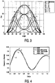
- Fig. 3 depicts computer-generated examples of the top-side far-field emitted light intensity (or flux) as a function of the direction of emission into silicone with respect to the normal to the LED, ⁇ 3 , defined in Fig. 2 .
- the curves in Fig. 3 are based on a single quantum well III-nitride device fabricated on a sapphire substrate with silicone as encapsulating gel 7.
- ⁇ n is the wavelength of the light in the semiconductor material separating the active region and the reflective contact.
- the units of flux are arbitrary as only the variations of flux with angle are of concern.
- the radiation patterns depend upon the distance, d, the wavelength of emitted light, and the effective indices of refraction of the materials through which the light passes in exiting from the LED, among other factors. The radiation patterns clearly change as d changes, changing the flux lying within the escape cone of 38.7°.
- a maximum in total emitted flux may occur for a radiation pattern not peaked about the central perpendicular axis of the light emitting region. That is, spacing the reflective plane from the light emitting region such that flux intensity is directed primarily normal to the surface (0 deg. in Fig. 3 or "on-axis") does not necessarily lead to maximum total emitted flux. Curve "f' in Fig. 3 provides marked on-axis peaking of emitted radiation, but at a considerable sacrifice in the total emitted flux. Thus, spacing the light emitting region from the reflector so as to maximize on-axis light emission intensity may be suboptimal for obtaining maximal LED total flux.
- Fig. 4 illustrates, for four devices, computer generated plots of extraction efficiency of total flux of a 1mm x 1mm flip chip as a function of distance between active region 1 and reflective contact 4 divided by ⁇ n .
- Curve a in Fig. 4 represents the results for a III-nitride single quantum well device with a sapphire substrate, a silicone encapsulating gel, and a reflective contact having silver/nickel contact.
- Fig. 4 illustrates the second and third maxima.
- the second maximum in extraction efficiency occurs between about 0.6 ⁇ n and about 0.75 ⁇ n
- the third maximum in extraction efficiency occurs between about 1.2 ⁇ n and about 1.35 ⁇ n .
- the center of a single quantum well active region 1 should be placed between about 0.5 ⁇ n and about 0.8 ⁇ n , or between about 1.1 ⁇ n and about 1.4 ⁇ n from reflective contact 4.
- the location of the maxima in a curve of extraction efficiency vs. distance may shift as the wavelength of the light changes.
- the wavelength of the light affects the phase shift due to reflection from the metal, ⁇ . If ⁇ is calculated from known n and k values, the calculation takes into account the wavelength. If ⁇ is measured as described above, ⁇ must be measured for a particular wavelength to ensure proper selection of the distance between the active region and the reflective contact.
- the table below lists spacing ranges d between a single III-nitride quantum well and a Ni/Ag contact corresponding to the second, third, and fourth maxima in a plot of extraction efficiency vs. d for three different wavelength devices.
- 450nm device 505 nm device 530 nm device n 2.4 d/ ⁇ n d/ ⁇ n d/ ⁇ n Optimal 0.5-0.8 0.53-0.83 0.55-0.85 Preferred 0.6-0.7 0.63-0.73 0.65-0.75 Optimal 1.05-1.35 1.08-1.38 1.1-1.4 Preferred 1.15-1.25 1.18-1.28 1.2-1.3 Optimal 1.6-1.9 1.63-1.93 1.65-1.95 Preferred 1.65-1.75 1.68-1.78 1.7-1.8
- a first maximum generally lies between about 0.1 ⁇ n and about 0.3 ⁇ n .
- a 450 nm III-nitride device with a pure silver contact has a second maximum in extraction efficiency between about 0.65 ⁇ n and about 0.75 ⁇ n , a third maximum in extraction efficiency between about 1.15 ⁇ n and about 1.38 ⁇ n , and a fourth maximum in extraction efficiency between about 1.73 ⁇ n , and about 1.85 ⁇ n .
- Fig. 5 illustrates a method for determining the spacing between the active region and reflective contact.
- the escape cone is calculated using the index of refraction of the semiconductor material, the substrate, and the encapsulation material or air, if no encapsulation material is used.
- the phase shift due to optical path length and phase shift due to reflection are then calculated or measured, as described above. The phase shift due to optical path length and phase shift due to reflection depend on the material used in the reflective contact and the wavelength of the light.
- the radiation pattern is calculated for various spacings between the active region and reflective contact using the phase shifts determined in stage 204, yielding a graph such as Fig. 3 . The radiation pattern depends on the wavelength of light.
- the extraction efficiency is calculated as a function of the distance d between the active region and the reflective contact.
- the extraction efficiency depends on the radiation pattern calculated in stage 206 and the escape cone calculated in stage 202.
- An example of extraction efficiency as a function of d is illustrated in Fig. 4 .
- the maxima in the plot of extraction efficiency as a function of d are identified in stage 210, which determine the spacing between the active region and the reflective contact which outputs the most light.
- the method illustrated in Fig. 5 is described in more detail in U.S. Application Serial No. 10/158,360 , titled "Selective Placement Of Quantum Wells In Flipchip Light Emitting Diodes For Improved Light Extraction," filed May 29, 2002, and incorporated herein by reference.
- III-phosphide devices may have an AlInP layer adjacent to the active region, and a GaInP contact layer adjacent to the reflective contact.
- the reflective contact is selected for ohmic contact with GaInP. Examples of suitable reflective contact materials are Al, Ag, and Au.
- the reflective contact metal may be alloyed to the GaInP, which may reduce the reflectivity of the contact.
- a two-part contact may be used.
- a layer of suitable ohmic metal is deposited and alloyed to the GaInP.
- the metal is etched into a pattern of fine lines whereby most of the surface area of the GaInP is revealed, the fine lines serving to conduct current into the device.
- the exposed areas of the GaInP are then chemically etched away revealing the AlInP cladding layer beneath, thereby eliminating a large part of the adsorbing GaInP from the optical path.
- a suitable reflector chosen for its optical properties without regard to the resistivity of the contact it makes to the AlInP, is deposited over both the fine lines of the first metal and the exposed AlInP. In this manner, current is conducted into the device by the first metal, and a highly reflective second metal serves as a mirror.
- Curve a of Fig. 4A presents data for a single quantum well active region.
- the methods described herein are not limited to single quantum well devices and can also be used in connection with multiple quantum well (MQW) active regions.
- MQW multiple quantum well
- the center of brightness and/or physical center of MQW active regions may be placed at a separation corresponding to a maximum on the appropriate plot of extraction efficiency of top-side flux as a function of distance between the active region and the reflective contact.
- MQW multiple quantum well
- the curve corresponding to a two quantum well active region corresponds to the second maximum in a plot of extraction efficiency vs. distance between the center of the active region and the p-electrode, and is located at a distance of about 0.67 ⁇ n .
- the extraction efficiency of a device can be improved by designing the active region and the layers between the active region and the reflective electrode such that each of the quantum wells are located as close as possible to a maximum on a plot of extraction efficiency vs. distance from the reflective electrode.
- Figs. 6A, 6B , 7A, and 7B illustrate examples of devices so designed.
- the device illustrated in Figs. 6A and 6B may be, for example, a III-nitride device emitting light at a wavelength ranging from UV through green.
- Each of quantum wells 15 may have a thickness ranging from about 10 angstroms to about 60 angstroms, usually has a thickness between about 15 angstroms to about 40 angstroms, and preferably has a thickness of about 30 angstroms.
- the composition of quantum wells 15 depends on the color of light to be emitted by the device.
- Each of quantum wells 15 need not have the same thickness and composition.
- Barrier layer 17 may have a thickness ranging from about 50 angstroms to about 200 angstroms, and usually has a thickness of about 85 angstroms.
- a barrier layer in a shorter wavelength device may be thinner than a barrier layer in a longer wavelength device.
- P-type region may contain, listed in order from the active region to the p-electrode, an AlGaN confining layer 5a, a first GaN layer 5b, and a second GaN contact layer 5c.
- confining layer 5a may have a thickness between 100 angstroms and 1000 angstroms, and usually has a thickness between about 100 angstroms to about 400 angstroms; first GaN layer 5b may have a thickness between about 100 angstroms and about 1000 angstroms, and usually has a thickness between about 400 angstroms and about 900 angstroms; and second GaN contact layer 5c may have a thickness between about 50 angstroms and about 500 angstroms, and usually has a thickness between about 50 angstroms and about 250 angstroms.
- the reflective p-electrode in the device illustrated in Figs. 6A and 6B may be, for example, a multi-layer electrode with a thin layer of Ni sandwiched between GaN contact layer 5c and a thick layer of Ag.
- the entire active region is located surrounding a peak on a curve of extraction efficiency vs. distance between the active region and the p-electrode.
- the placement of the active region may correspond to the third or a higher local maximum.
- the active region is not placed near the first maximum, since placement of the active region at the first maximum may result in a p-type region that is too thin.
- the fourth and higher maxima are not used as such placement may result in a p-type region that is too thick, and a decrease in extraction efficiency.
- the p-type region is generally fabricated at a higher temperature than the quantum wells, thus the fabrication of a thick p-type region may result in fabrication conditions that damage the quantum wells.
- the extraction efficiency beyond the fourth local maximum is significantly lower than for the second, third, and fourth local maxima.
- the center of the middle quantum well is optimally located at a distance from the p-electrode corresponding to a peak on a curve of extraction efficiency vs. distance.
- the total thickness of the active region is limited such that all of the active region is close to the peak on the curve of extraction efficiency vs. distance between the active region and the p-electrode.
- the total thickness of the active region may be selected such that the active region may not be larger than 0.35 ⁇ n and is usually not larger than 0.15 ⁇ n , and usually does not extend beyond 0.05 ⁇ n on either side of the peak.
- the four curves in Fig. 4 demonstrate that as the active region becomes more compact, the total extraction efficiency improves.
- Fig. 4 illustrates the extraction efficiency of four devices, a single quantum well device (curve a), a two quantum well device with a thin barrier (curve b), a two quantum well device with a thick barrier (curve c), and a four quantum well device.
- the device with the most compact active region has the highest extraction efficiency
- the device with the thickest active region the four quantum well device
- the center of brightness of the active region is expected to be the physical center of the active region.
- the center of brightness may not be the physical center of the active region.
- the center of brightness of the active region may be located at a peak on a curve of extraction efficiency vs. distance.
- the quantum wells in the active region may be clustered around peaks on a curve of extraction efficiency vs. distance, with thin barrier layers separating the quantum wells in each cluster and thick barrier layers separating the clusters.
- the center of brightness of each cluster may be placed at a separation corresponding to a maximum on the appropriate plot of extraction efficiency of top-side flux as a function of distance between the active region and the reflective contact.
- Figs. 7A and 7B illustrate such a device.
- the device illustrated in Fig. 7A has two clusters of quantum wells, each with two quantum wells.
- the first cluster includes two quantum wells 15a separated by a barrier layer 17a, the center of which is located at the first peak shown in Fig. 4 (the second local maximum).
- the second cluster includes two quantum wells 15b separated by a barrier layer 17b, the center of which is located at the second peak shown in Fig. 4 (the third local maximum).
- the two clusters are separated by a thick barrier layer 17c.
- the clusters may have more or fewer than two quantum wells, and need not have the same number of quantum wells.
- Fig. 9 is an exploded view of a packaged light emitting device.
- a heat-sinking slug 100 is placed into an insert-molded leadframe 106.
- the insert-molded leadframe 106 is, for example, a filled plastic material molded around a metal frame that provides an electrical path.
- Slug 100 may include an optional reflector cup 102. Alternatively, slug 100 may provide a pedestal without a reflector cup.
- the light emitting device die 104 which may be any of the devices described above, is mounted directly or indirectly via a thermally conducting submount 103 to slug 100.
- An optical lens 108 may be added.
Landscapes
- Led Devices (AREA)
- Led Device Packages (AREA)
Applications Claiming Priority (3)
| Application Number | Priority Date | Filing Date | Title |
|---|---|---|---|
| US43583802P | 2002-12-20 | 2002-12-20 | |
| US10/632,720 US6900474B2 (en) | 2002-12-20 | 2003-07-31 | Light emitting devices with compact active regions |
| EP03104574A EP1432046A3 (en) | 2002-12-20 | 2003-12-08 | LED with improved light extraction |
Related Parent Applications (1)
| Application Number | Title | Priority Date | Filing Date |
|---|---|---|---|
| EP03104574A Division EP1432046A3 (en) | 2002-12-20 | 2003-12-08 | LED with improved light extraction |
Publications (1)
| Publication Number | Publication Date |
|---|---|
| EP3435427A1 true EP3435427A1 (en) | 2019-01-30 |
Family
ID=32397268
Family Applications (2)
| Application Number | Title | Priority Date | Filing Date |
|---|---|---|---|
| EP18188922.1A Ceased EP3435427A1 (en) | 2002-12-20 | 2003-12-08 | Light emitting devices with compact active regions |
| EP03104574A Ceased EP1432046A3 (en) | 2002-12-20 | 2003-12-08 | LED with improved light extraction |
Family Applications After (1)
| Application Number | Title | Priority Date | Filing Date |
|---|---|---|---|
| EP03104574A Ceased EP1432046A3 (en) | 2002-12-20 | 2003-12-08 | LED with improved light extraction |
Country Status (4)
| Country | Link |
|---|---|
| US (2) | US6900474B2 (https=) |
| EP (2) | EP3435427A1 (https=) |
| JP (1) | JP2004207742A (https=) |
| TW (1) | TWI336527B (https=) |
Families Citing this family (26)
| Publication number | Priority date | Publication date | Assignee | Title |
|---|---|---|---|---|
| US7087936B2 (en) * | 2003-04-30 | 2006-08-08 | Cree, Inc. | Methods of forming light-emitting devices having an antireflective layer that has a graded index of refraction |
| JP2005167091A (ja) * | 2003-12-04 | 2005-06-23 | Nitto Denko Corp | 光半導体装置 |
| US20060081859A1 (en) * | 2004-10-15 | 2006-04-20 | Shyi-Ming Pan | Light emitting semiconductor bonding structure and method of manufacturing the same |
| JP5356810B2 (ja) * | 2005-06-14 | 2013-12-04 | コーニンクレッカ フィリップス エヌ ヴェ | マルチビュー表示装置 |
| JP2007142289A (ja) * | 2005-11-21 | 2007-06-07 | Sharp Corp | 発光装置 |
| JP2009530798A (ja) | 2006-01-05 | 2009-08-27 | イルミテックス, インコーポレイテッド | Ledから光を導くための独立した光学デバイス |
| KR100736623B1 (ko) | 2006-05-08 | 2007-07-09 | 엘지전자 주식회사 | 수직형 발광 소자 및 그 제조방법 |
| US8008676B2 (en) | 2006-05-26 | 2011-08-30 | Cree, Inc. | Solid state light emitting device and method of making same |
| US7789531B2 (en) | 2006-10-02 | 2010-09-07 | Illumitex, Inc. | LED system and method |
| JP4276684B2 (ja) * | 2007-03-27 | 2009-06-10 | 株式会社東芝 | 半導体発光装置及びその製造方法 |
| CN101939849A (zh) | 2008-02-08 | 2011-01-05 | 伊鲁米特克有限公司 | 用于发射器层成形的系统和方法 |
| US8354687B1 (en) * | 2008-07-30 | 2013-01-15 | Nitek, Inc. | Efficient thermal management and packaging for group III nitride based UV devices |
| TW201034256A (en) | 2008-12-11 | 2010-09-16 | Illumitex Inc | Systems and methods for packaging light-emitting diode devices |
| WO2010116703A1 (ja) * | 2009-04-06 | 2010-10-14 | パナソニック株式会社 | 窒化物系半導体素子およびその製造方法 |
| KR101064011B1 (ko) * | 2009-04-28 | 2011-09-08 | 엘지이노텍 주식회사 | 발광소자 및 그 제조방법 |
| US8585253B2 (en) | 2009-08-20 | 2013-11-19 | Illumitex, Inc. | System and method for color mixing lens array |
| US8449128B2 (en) | 2009-08-20 | 2013-05-28 | Illumitex, Inc. | System and method for a lens and phosphor layer |
| KR100999771B1 (ko) * | 2010-02-25 | 2010-12-08 | 엘지이노텍 주식회사 | 발광 소자, 발광 소자 제조방법 및 발광 소자 패키지 |
| KR101039948B1 (ko) * | 2010-04-23 | 2011-06-09 | 엘지이노텍 주식회사 | 발광 소자, 발광 소자 제조방법 및 발광 소자 패키지 |
| JP2012227122A (ja) * | 2011-04-04 | 2012-11-15 | Rohm Co Ltd | 有機el装置 |
| KR20140090346A (ko) * | 2013-01-07 | 2014-07-17 | 삼성전자주식회사 | 반도체 발광 소자 |
| KR102172934B1 (ko) * | 2013-07-22 | 2020-11-03 | 루미리즈 홀딩 비.브이. | 플립-칩 측면 방출 led |
| KR102212561B1 (ko) * | 2014-08-11 | 2021-02-08 | 삼성전자주식회사 | 반도체 발광 소자 및 반도체 발광 소자 패키지 |
| WO2017164036A1 (ja) * | 2016-03-24 | 2017-09-28 | スタンレー電気株式会社 | Iii族窒化物積層体の製造方法 |
| JP6727185B2 (ja) | 2017-12-28 | 2020-07-22 | 日機装株式会社 | 窒化物半導体発光素子 |
| JP2022172792A (ja) * | 2021-05-07 | 2022-11-17 | 日機装株式会社 | 窒化物半導体発光素子 |
Citations (3)
| Publication number | Priority date | Publication date | Assignee | Title |
|---|---|---|---|---|
| US5410159A (en) * | 1992-09-30 | 1995-04-25 | Kabushiki Kaisha Toshiba | Light-emitting diode |
| JP2000091635A (ja) * | 1995-09-29 | 2000-03-31 | Nichia Chem Ind Ltd | 窒化物半導体発光素子 |
| US20020190260A1 (en) * | 1999-12-22 | 2002-12-19 | Yu-Chen Shen | Selective placement of quantum wells in flipchip light emitting diodes for improved light extraction |
Family Cites Families (10)
| Publication number | Priority date | Publication date | Assignee | Title |
|---|---|---|---|---|
| CA2030368C (en) | 1989-11-22 | 2000-03-28 | Daido Tokushuko Kabushiki Kaisha | Light-emitting diode having light reflecting layer |
| JPH05190901A (ja) * | 1992-01-17 | 1993-07-30 | Sharp Corp | 半導体発光素子とその製造方法 |
| US5362977A (en) * | 1992-12-28 | 1994-11-08 | At&T Bell Laboratories | Single mirror light-emitting diodes with enhanced intensity |
| US5537433A (en) | 1993-07-22 | 1996-07-16 | Sharp Kabushiki Kaisha | Semiconductor light emitter |
| JP3304787B2 (ja) * | 1996-09-08 | 2002-07-22 | 豊田合成株式会社 | 半導体発光素子及びその製造方法 |
| EP1129492B1 (de) * | 1998-09-30 | 2014-04-09 | OSRAM Opto Semiconductors GmbH | Oberflächenemittierende diodenstrahlungsquelle |
| JP2000299493A (ja) * | 1999-04-15 | 2000-10-24 | Daido Steel Co Ltd | 半導体面発光素子 |
| JP2001053336A (ja) * | 1999-08-05 | 2001-02-23 | Toyoda Gosei Co Ltd | Iii族窒化物系化合物半導体発光素子 |
| EP2270875B1 (de) * | 2000-04-26 | 2018-01-10 | OSRAM Opto Semiconductors GmbH | Strahlungsmittierendes Halbleiterbauelement und dessen Herstellungsverfahren |
| US6753214B1 (en) * | 2001-02-16 | 2004-06-22 | Optical Communication Products, Inc. | Photodetector with isolation implant region for reduced device capacitance and increased bandwidth |
-
2003
- 2003-07-31 US US10/632,720 patent/US6900474B2/en not_active Expired - Lifetime
- 2003-12-08 EP EP18188922.1A patent/EP3435427A1/en not_active Ceased
- 2003-12-08 EP EP03104574A patent/EP1432046A3/en not_active Ceased
- 2003-12-17 TW TW092135747A patent/TWI336527B/zh not_active IP Right Cessation
- 2003-12-22 JP JP2003425621A patent/JP2004207742A/ja not_active Revoked
-
2005
- 2005-05-27 US US11/139,325 patent/US7719018B2/en not_active Expired - Lifetime
Patent Citations (3)
| Publication number | Priority date | Publication date | Assignee | Title |
|---|---|---|---|---|
| US5410159A (en) * | 1992-09-30 | 1995-04-25 | Kabushiki Kaisha Toshiba | Light-emitting diode |
| JP2000091635A (ja) * | 1995-09-29 | 2000-03-31 | Nichia Chem Ind Ltd | 窒化物半導体発光素子 |
| US20020190260A1 (en) * | 1999-12-22 | 2002-12-19 | Yu-Chen Shen | Selective placement of quantum wells in flipchip light emitting diodes for improved light extraction |
Non-Patent Citations (3)
| Title |
|---|
| KRISTIAAN NEYTS: "Electroluminescence II", vol. 65, article "Microcavities for Electroluminescent Devices" |
| MAX BORN; EMIL WOLF, PRINCIPLES OF OPTICS, 1980, pages 628 - 630 |
| P. MAASKANT ET AL.: "Fabrication of GaN-based Resonant Cavity LEDs", P . S . SOL., 19 February 2002 (2002-02-19) |
Also Published As
| Publication number | Publication date |
|---|---|
| US7719018B2 (en) | 2010-05-18 |
| EP1432046A3 (en) | 2004-07-14 |
| JP2004207742A (ja) | 2004-07-22 |
| US20050212005A1 (en) | 2005-09-29 |
| TW200503291A (en) | 2005-01-16 |
| TWI336527B (en) | 2011-01-21 |
| US6900474B2 (en) | 2005-05-31 |
| US20040119077A1 (en) | 2004-06-24 |
| EP1432046A2 (en) | 2004-06-23 |
Similar Documents
| Publication | Publication Date | Title |
|---|---|---|
| US6900474B2 (en) | Light emitting devices with compact active regions | |
| US11563149B2 (en) | Light-emitting device | |
| US6903376B2 (en) | Selective placement of quantum wells in flipchip light emitting diodes for improved light extraction | |
| US9299884B2 (en) | Light emitting device and light emitting device package including the same | |
| US7825006B2 (en) | Lift-off process for GaN films formed on SiC substrates and devices fabricated using the method | |
| JP6530442B2 (ja) | 反射構造を有する半導体発光ダイオードおよびその製造方法 | |
| US10199360B2 (en) | Wire bond free wafer level LED | |
| US6133589A (en) | AlGaInN-based LED having thick epitaxial layer for improved light extraction | |
| US20100038669A1 (en) | Vertical light emitting diodes | |
| KR20070013324A (ko) | 3족 질화물 소자를 제조하는 방법 및 그 방법을 이용하여제조된 소자 | |
| US20250126936A1 (en) | Light-emitting device and manufacturing method thereof | |
| US20050045893A1 (en) | Resonant cavity light emitting device | |
| US20250185423A1 (en) | Light-emitting device | |
| TWI718358B (zh) | 發光元件 | |
| KR101064011B1 (ko) | 발광소자 및 그 제조방법 | |
| US12243966B2 (en) | Light-emitting device | |
| US20240170610A1 (en) | Light-emitting element, light-emitting module and display backlight unit | |
| US12550514B2 (en) | Light-emitting device with cavity between top electrode pad and protective layer | |
| CN100433387C (zh) | 发光二极管芯片 | |
| US20250318326A1 (en) | Semiconductor device and semiconductor module having the same |
Legal Events
| Date | Code | Title | Description |
|---|---|---|---|
| PUAI | Public reference made under article 153(3) epc to a published international application that has entered the european phase |
Free format text: ORIGINAL CODE: 0009012 |
|
| STAA | Information on the status of an ep patent application or granted ep patent |
Free format text: STATUS: THE APPLICATION HAS BEEN PUBLISHED |
|
| AC | Divisional application: reference to earlier application |
Ref document number: 1432046 Country of ref document: EP Kind code of ref document: P |
|
| AK | Designated contracting states |
Kind code of ref document: A1 Designated state(s): DE |
|
| STAA | Information on the status of an ep patent application or granted ep patent |
Free format text: STATUS: REQUEST FOR EXAMINATION WAS MADE |
|
| STAA | Information on the status of an ep patent application or granted ep patent |
Free format text: STATUS: EXAMINATION IS IN PROGRESS |
|
| 17P | Request for examination filed |
Effective date: 20190730 |
|
| RBV | Designated contracting states (corrected) |
Designated state(s): DE |
|
| 17Q | First examination report despatched |
Effective date: 20190827 |
|
| STAA | Information on the status of an ep patent application or granted ep patent |
Free format text: STATUS: THE APPLICATION HAS BEEN REFUSED |
|
| 18R | Application refused |
Effective date: 20200828 |