EP3428986A1 - Stabile und leistungsstarke elektrolumineszente materialien - Google Patents
Stabile und leistungsstarke elektrolumineszente materialien Download PDFInfo
- Publication number
- EP3428986A1 EP3428986A1 EP18190646.2A EP18190646A EP3428986A1 EP 3428986 A1 EP3428986 A1 EP 3428986A1 EP 18190646 A EP18190646 A EP 18190646A EP 3428986 A1 EP3428986 A1 EP 3428986A1
- Authority
- EP
- European Patent Office
- Prior art keywords
- ring
- compound
- alkyl
- metal
- emissive
- Prior art date
- Legal status (The legal status is an assumption and is not a legal conclusion. Google has not performed a legal analysis and makes no representation as to the accuracy of the status listed.)
- Granted
Links
- 239000000463 material Substances 0.000 title claims description 234
- 239000003446 ligand Substances 0.000 claims abstract description 137
- 125000000217 alkyl group Chemical group 0.000 claims abstract description 107
- 125000003118 aryl group Chemical group 0.000 claims abstract description 98
- 150000001875 compounds Chemical class 0.000 claims description 176
- 229910052751 metal Inorganic materials 0.000 claims description 133
- 239000002184 metal Substances 0.000 claims description 131
- 125000001424 substituent group Chemical group 0.000 claims description 97
- 125000001072 heteroaryl group Chemical group 0.000 claims description 84
- 125000003342 alkenyl group Chemical group 0.000 claims description 79
- 125000000304 alkynyl group Chemical group 0.000 claims description 77
- 125000004404 heteroalkyl group Chemical group 0.000 claims description 60
- 229910052741 iridium Inorganic materials 0.000 claims description 60
- 229910052757 nitrogen Inorganic materials 0.000 claims description 59
- 125000001997 phenyl group Chemical group [H]C1=C([H])C([H])=C(*)C([H])=C1[H] 0.000 claims description 56
- 125000006615 aromatic heterocyclic group Chemical group 0.000 claims description 32
- 229910052799 carbon Inorganic materials 0.000 claims description 32
- 125000003710 aryl alkyl group Chemical group 0.000 claims description 31
- 229910052739 hydrogen Inorganic materials 0.000 claims description 29
- 229910052697 platinum Inorganic materials 0.000 claims description 29
- 125000005843 halogen group Chemical group 0.000 claims description 21
- 125000000623 heterocyclic group Chemical group 0.000 claims description 21
- -1 fluoro-substituted phenyl ring Chemical group 0.000 claims description 20
- 229910052763 palladium Inorganic materials 0.000 claims description 19
- 229910052703 rhodium Inorganic materials 0.000 claims description 19
- 125000002877 alkyl aryl group Chemical group 0.000 claims description 17
- 229910052736 halogen Inorganic materials 0.000 claims description 16
- 150000002367 halogens Chemical class 0.000 claims description 16
- 125000004433 nitrogen atom Chemical group N* 0.000 claims description 15
- 125000003107 substituted aryl group Chemical group 0.000 claims description 15
- 125000005647 linker group Chemical group 0.000 claims description 12
- 125000001153 fluoro group Chemical group F* 0.000 claims description 7
- 230000005693 optoelectronics Effects 0.000 claims description 7
- 125000004432 carbon atom Chemical group C* 0.000 claims description 5
- 238000005286 illumination Methods 0.000 claims description 3
- 230000011664 signaling Effects 0.000 claims description 2
- VQGHOUODWALEFC-UHFFFAOYSA-N alpha-Phenylpyridine Natural products C1=CC=CC=C1C1=CC=CC=N1 VQGHOUODWALEFC-UHFFFAOYSA-N 0.000 abstract description 15
- JVZRCNQLWOELDU-UHFFFAOYSA-N gamma-Phenylpyridine Natural products C1=CC=CC=C1C1=CC=NC=C1 JVZRCNQLWOELDU-UHFFFAOYSA-N 0.000 abstract description 4
- 150000005359 phenylpyridines Chemical class 0.000 abstract 1
- 239000010410 layer Substances 0.000 description 188
- XEKOWRVHYACXOJ-UHFFFAOYSA-N Ethyl acetate Chemical compound CCOC(C)=O XEKOWRVHYACXOJ-UHFFFAOYSA-N 0.000 description 101
- VLKZOEOYAKHREP-UHFFFAOYSA-N n-Hexane Chemical class CCCCCC VLKZOEOYAKHREP-UHFFFAOYSA-N 0.000 description 93
- IJGRMHOSHXDMSA-UHFFFAOYSA-N Atomic nitrogen Chemical compound N#N IJGRMHOSHXDMSA-UHFFFAOYSA-N 0.000 description 84
- OKKJLVBELUTLKV-UHFFFAOYSA-N Methanol Chemical compound OC OKKJLVBELUTLKV-UHFFFAOYSA-N 0.000 description 75
- 239000007983 Tris buffer Substances 0.000 description 69
- YMWUJEATGCHHMB-UHFFFAOYSA-N Dichloromethane Chemical compound ClCCl YMWUJEATGCHHMB-UHFFFAOYSA-N 0.000 description 63
- 239000000047 product Substances 0.000 description 52
- MILUBEOXRNEUHS-UHFFFAOYSA-N iridium(3+) Chemical compound [Ir+3] MILUBEOXRNEUHS-UHFFFAOYSA-N 0.000 description 51
- 239000011541 reaction mixture Substances 0.000 description 50
- 238000010992 reflux Methods 0.000 description 49
- TVIVIEFSHFOWTE-UHFFFAOYSA-K tri(quinolin-8-yloxy)alumane Chemical compound [Al+3].C1=CN=C2C([O-])=CC=CC2=C1.C1=CN=C2C([O-])=CC=CC2=C1.C1=CN=C2C([O-])=CC=CC2=C1 TVIVIEFSHFOWTE-UHFFFAOYSA-K 0.000 description 49
- LYCAIKOWRPUZTN-UHFFFAOYSA-N Ethylene glycol Chemical compound OCCO LYCAIKOWRPUZTN-UHFFFAOYSA-N 0.000 description 42
- 239000000243 solution Substances 0.000 description 39
- 239000012044 organic layer Substances 0.000 description 38
- 230000000052 comparative effect Effects 0.000 description 35
- 235000019439 ethyl acetate Nutrition 0.000 description 34
- 229940093499 ethyl acetate Drugs 0.000 description 33
- XLYOFNOQVPJJNP-UHFFFAOYSA-N water Substances O XLYOFNOQVPJJNP-UHFFFAOYSA-N 0.000 description 33
- 239000000203 mixture Substances 0.000 description 31
- GKOZUEZYRPOHIO-UHFFFAOYSA-N iridium atom Chemical compound [Ir] GKOZUEZYRPOHIO-UHFFFAOYSA-N 0.000 description 30
- BWHMMNNQKKPAPP-UHFFFAOYSA-L potassium carbonate Chemical compound [K+].[K+].[O-]C([O-])=O BWHMMNNQKKPAPP-UHFFFAOYSA-L 0.000 description 30
- YXVFYQXJAXKLAK-UHFFFAOYSA-M 4-phenylphenolate Chemical compound C1=CC([O-])=CC=C1C1=CC=CC=C1 YXVFYQXJAXKLAK-UHFFFAOYSA-M 0.000 description 29
- KDLHZDBZIXYQEI-UHFFFAOYSA-N palladium Substances [Pd] KDLHZDBZIXYQEI-UHFFFAOYSA-N 0.000 description 29
- 230000032258 transport Effects 0.000 description 29
- REDXJYDRNCIFBQ-UHFFFAOYSA-N aluminium(3+) Chemical compound [Al+3] REDXJYDRNCIFBQ-UHFFFAOYSA-N 0.000 description 28
- VYPSYNLAJGMNEJ-UHFFFAOYSA-N Silicium dioxide Chemical compound O=[Si]=O VYPSYNLAJGMNEJ-UHFFFAOYSA-N 0.000 description 27
- VFUDMQLBKNMONU-UHFFFAOYSA-N 9-[4-(4-carbazol-9-ylphenyl)phenyl]carbazole Chemical compound C12=CC=CC=C2C2=CC=CC=C2N1C1=CC=C(C=2C=CC(=CC=2)N2C3=CC=CC=C3C3=CC=CC=C32)C=C1 VFUDMQLBKNMONU-UHFFFAOYSA-N 0.000 description 26
- CSNNHWWHGAXBCP-UHFFFAOYSA-L Magnesium sulfate Chemical compound [Mg+2].[O-][S+2]([O-])([O-])[O-] CSNNHWWHGAXBCP-UHFFFAOYSA-L 0.000 description 26
- 239000000758 substrate Substances 0.000 description 26
- 238000002347 injection Methods 0.000 description 25
- 239000007924 injection Substances 0.000 description 25
- 239000007788 liquid Substances 0.000 description 25
- 239000000741 silica gel Substances 0.000 description 24
- 229910002027 silica gel Inorganic materials 0.000 description 24
- 238000003756 stirring Methods 0.000 description 24
- 239000007787 solid Substances 0.000 description 23
- 230000015572 biosynthetic process Effects 0.000 description 22
- 238000003786 synthesis reaction Methods 0.000 description 22
- 238000003828 vacuum filtration Methods 0.000 description 21
- XTHFKEDIFFGKHM-UHFFFAOYSA-N Dimethoxyethane Chemical compound COCCOC XTHFKEDIFFGKHM-UHFFFAOYSA-N 0.000 description 20
- 239000003480 eluent Substances 0.000 description 20
- 238000001704 evaporation Methods 0.000 description 20
- 230000008020 evaporation Effects 0.000 description 20
- 125000002496 methyl group Chemical group [H]C([H])([H])* 0.000 description 20
- 150000003384 small molecules Chemical class 0.000 description 20
- RIOQSEWOXXDEQQ-UHFFFAOYSA-N triphenylphosphine Chemical compound C1=CC=CC=C1P(C=1C=CC=CC=1)C1=CC=CC=C1 RIOQSEWOXXDEQQ-UHFFFAOYSA-N 0.000 description 20
- 239000002019 doping agent Substances 0.000 description 19
- HLYTZTFNIRBLNA-LNTINUHCSA-K iridium(3+);(z)-4-oxopent-2-en-2-olate Chemical compound [Ir+3].C\C([O-])=C\C(C)=O.C\C([O-])=C\C(C)=O.C\C([O-])=C\C(C)=O HLYTZTFNIRBLNA-LNTINUHCSA-K 0.000 description 18
- 238000010898 silica gel chromatography Methods 0.000 description 16
- YXFVVABEGXRONW-UHFFFAOYSA-N Toluene Chemical compound CC1=CC=CC=C1 YXFVVABEGXRONW-UHFFFAOYSA-N 0.000 description 15
- 150000001721 carbon Chemical group 0.000 description 15
- 238000006243 chemical reaction Methods 0.000 description 15
- 238000000034 method Methods 0.000 description 15
- 229910000027 potassium carbonate Inorganic materials 0.000 description 15
- 239000002904 solvent Substances 0.000 description 15
- IWUVCNQOYRJIAB-UHFFFAOYSA-N 2-(3-bromophenyl)-5-methylpyridine Chemical compound N1=CC(C)=CC=C1C1=CC=CC(Br)=C1 IWUVCNQOYRJIAB-UHFFFAOYSA-N 0.000 description 14
- WYURNTSHIVDZCO-UHFFFAOYSA-N Tetrahydrofuran Chemical compound C1CCOC1 WYURNTSHIVDZCO-UHFFFAOYSA-N 0.000 description 14
- 230000005525 hole transport Effects 0.000 description 14
- 239000012074 organic phase Substances 0.000 description 14
- 239000002244 precipitate Substances 0.000 description 14
- 229910052943 magnesium sulfate Inorganic materials 0.000 description 13
- 235000019341 magnesium sulphate Nutrition 0.000 description 13
- JUJWROOIHBZHMG-UHFFFAOYSA-N Pyridine Chemical compound C1=CC=NC=C1 JUJWROOIHBZHMG-UHFFFAOYSA-N 0.000 description 12
- HEMHJVSKTPXQMS-UHFFFAOYSA-M Sodium hydroxide Chemical compound [OH-].[Na+] HEMHJVSKTPXQMS-UHFFFAOYSA-M 0.000 description 12
- 230000000903 blocking effect Effects 0.000 description 12
- 239000000539 dimer Substances 0.000 description 12
- 238000004519 manufacturing process Methods 0.000 description 12
- 239000011368 organic material Substances 0.000 description 12
- HXITXNWTGFUOAU-UHFFFAOYSA-N phenylboronic acid Chemical compound OB(O)C1=CC=CC=C1 HXITXNWTGFUOAU-UHFFFAOYSA-N 0.000 description 12
- 238000000746 purification Methods 0.000 description 12
- LPXPTNMVRIOKMN-UHFFFAOYSA-M sodium nitrite Chemical compound [Na+].[O-]N=O LPXPTNMVRIOKMN-UHFFFAOYSA-M 0.000 description 12
- 238000006467 substitution reaction Methods 0.000 description 12
- 0 *C1c(cccc2)c2C(c2ccccc2C2)=*2C1 Chemical compound *C1c(cccc2)c2C(c2ccccc2C2)=*2C1 0.000 description 11
- 238000004768 lowest unoccupied molecular orbital Methods 0.000 description 11
- 239000011241 protective layer Substances 0.000 description 11
- 239000000725 suspension Substances 0.000 description 11
- UHOVQNZJYSORNB-UHFFFAOYSA-N benzene Substances C1=CC=CC=C1 UHOVQNZJYSORNB-UHFFFAOYSA-N 0.000 description 10
- 238000000151 deposition Methods 0.000 description 10
- 238000001194 electroluminescence spectrum Methods 0.000 description 10
- 238000004770 highest occupied molecular orbital Methods 0.000 description 10
- 239000012299 nitrogen atmosphere Substances 0.000 description 10
- YJVFFLUZDVXJQI-UHFFFAOYSA-L palladium(ii) acetate Chemical compound [Pd+2].CC([O-])=O.CC([O-])=O YJVFFLUZDVXJQI-UHFFFAOYSA-L 0.000 description 10
- 229920000642 polymer Polymers 0.000 description 10
- LXNAVEXFUKBNMK-UHFFFAOYSA-N palladium(II) acetate Substances [Pd].CC(O)=O.CC(O)=O LXNAVEXFUKBNMK-UHFFFAOYSA-N 0.000 description 9
- YWNJQQNBJQUKME-UHFFFAOYSA-N 2-bromo-5-methylpyridine Chemical compound CC1=CC=C(Br)N=C1 YWNJQQNBJQUKME-UHFFFAOYSA-N 0.000 description 8
- ZNQVEEAIQZEUHB-UHFFFAOYSA-N 2-ethoxyethanol Chemical compound CCOCCO ZNQVEEAIQZEUHB-UHFFFAOYSA-N 0.000 description 8
- 229940093475 2-ethoxyethanol Drugs 0.000 description 8
- RTZKZFJDLAIYFH-UHFFFAOYSA-N Diethyl ether Chemical compound CCOCC RTZKZFJDLAIYFH-UHFFFAOYSA-N 0.000 description 8
- CDBYLPFSWZWCQE-UHFFFAOYSA-L Sodium Carbonate Chemical compound [Na+].[Na+].[O-]C([O-])=O CDBYLPFSWZWCQE-UHFFFAOYSA-L 0.000 description 8
- 238000006069 Suzuki reaction reaction Methods 0.000 description 8
- 238000005292 vacuum distillation Methods 0.000 description 8
- VLVFLDBJTBHJQN-UHFFFAOYSA-N 2-[3-(2-fluorophenyl)phenyl]pyridine iridium(3+) Chemical compound [Ir+3].FC1=CC=CC=C1C1=CC=CC(C=2N=CC=CC=2)=C1.FC1=CC=CC=C1C1=CC=CC(C=2N=CC=CC=2)=C1.FC1=CC=CC=C1C1=CC=CC(C=2N=CC=CC=2)=C1 VLVFLDBJTBHJQN-UHFFFAOYSA-N 0.000 description 7
- AGQLSVGMHSEHRH-UHFFFAOYSA-N 2-[3-(2-methylphenyl)phenyl]pyridine Chemical compound CC1=CC=CC=C1C1=CC=CC(C=2N=CC=CC=2)=C1 AGQLSVGMHSEHRH-UHFFFAOYSA-N 0.000 description 7
- XCJYREBRNVKWGJ-UHFFFAOYSA-N copper(II) phthalocyanine Chemical compound [Cu+2].C12=CC=CC=C2C(N=C2[N-]C(C3=CC=CC=C32)=N2)=NC1=NC([C]1C=CC=CC1=1)=NC=1N=C1[C]3C=CC=CC3=C2[N-]1 XCJYREBRNVKWGJ-UHFFFAOYSA-N 0.000 description 7
- 125000000753 cycloalkyl group Chemical group 0.000 description 7
- 230000005281 excited state Effects 0.000 description 7
- 230000006872 improvement Effects 0.000 description 7
- 230000007246 mechanism Effects 0.000 description 7
- 230000008569 process Effects 0.000 description 7
- MCIPELGMHYHVBA-UHFFFAOYSA-N 3,4-dimethyl-2-phenylpyridine Chemical compound CC1=CC=NC(C=2C=CC=CC=2)=C1C MCIPELGMHYHVBA-UHFFFAOYSA-N 0.000 description 6
- LMGVDGBKURRIHA-UHFFFAOYSA-N 4,5-dimethyl-2-phenylpyridine Chemical compound C1=C(C)C(C)=CN=C1C1=CC=CC=C1 LMGVDGBKURRIHA-UHFFFAOYSA-N 0.000 description 6
- WEVYAHXRMPXWCK-UHFFFAOYSA-N Acetonitrile Chemical compound CC#N WEVYAHXRMPXWCK-UHFFFAOYSA-N 0.000 description 6
- YRKCREAYFQTBPV-UHFFFAOYSA-N acetylacetone Chemical compound CC(=O)CC(C)=O YRKCREAYFQTBPV-UHFFFAOYSA-N 0.000 description 6
- 150000004945 aromatic hydrocarbons Chemical class 0.000 description 6
- 239000002800 charge carrier Substances 0.000 description 6
- 238000001816 cooling Methods 0.000 description 6
- 239000012043 crude product Substances 0.000 description 6
- 239000000412 dendrimer Substances 0.000 description 6
- 229920000736 dendritic polymer Polymers 0.000 description 6
- 125000002524 organometallic group Chemical group 0.000 description 6
- UMJSCPRVCHMLSP-UHFFFAOYSA-N pyridine Natural products COC1=CC=CN=C1 UMJSCPRVCHMLSP-UHFFFAOYSA-N 0.000 description 6
- 239000000523 sample Substances 0.000 description 6
- 239000000126 substance Substances 0.000 description 6
- RYRDKQYQAMRCHF-UHFFFAOYSA-N 3-methyl-2-(4-methylphenyl)pyridine Chemical compound C1=CC(C)=CC=C1C1=NC=CC=C1C RYRDKQYQAMRCHF-UHFFFAOYSA-N 0.000 description 5
- FQUOLAWBNANVNG-UHFFFAOYSA-N 5-tert-butyl-2-(3-phenylphenyl)pyridine Chemical compound N1=CC(C(C)(C)C)=CC=C1C1=CC=CC(C=2C=CC=CC=2)=C1 FQUOLAWBNANVNG-UHFFFAOYSA-N 0.000 description 5
- 239000008346 aqueous phase Substances 0.000 description 5
- 125000004429 atom Chemical group 0.000 description 5
- 239000010406 cathode material Substances 0.000 description 5
- 230000008021 deposition Effects 0.000 description 5
- 238000001035 drying Methods 0.000 description 5
- 229910052731 fluorine Inorganic materials 0.000 description 5
- 125000005842 heteroatom Chemical group 0.000 description 5
- AMGQUBHHOARCQH-UHFFFAOYSA-N indium;oxotin Chemical compound [In].[Sn]=O AMGQUBHHOARCQH-UHFFFAOYSA-N 0.000 description 5
- 238000012856 packing Methods 0.000 description 5
- 125000000999 tert-butyl group Chemical group [H]C([H])([H])C(*)(C([H])([H])[H])C([H])([H])[H] 0.000 description 5
- 238000002207 thermal evaporation Methods 0.000 description 5
- 230000007704 transition Effects 0.000 description 5
- AFSSVCNPDKKSRR-UHFFFAOYSA-N (3-bromophenyl)boronic acid Chemical compound OB(O)C1=CC=CC(Br)=C1 AFSSVCNPDKKSRR-UHFFFAOYSA-N 0.000 description 4
- GOXICVKOZJFRMB-UHFFFAOYSA-N (3-phenylphenyl)boronic acid Chemical compound OB(O)C1=CC=CC(C=2C=CC=CC=2)=C1 GOXICVKOZJFRMB-UHFFFAOYSA-N 0.000 description 4
- WLPFTJXVEBANAM-UHFFFAOYSA-N 2-(3-bromophenyl)pyridine Chemical compound BrC1=CC=CC(C=2N=CC=CC=2)=C1 WLPFTJXVEBANAM-UHFFFAOYSA-N 0.000 description 4
- KJNZQKYSNAQLEO-UHFFFAOYSA-N 2-(4-methylphenyl)pyridine Chemical compound C1=CC(C)=CC=C1C1=CC=CC=N1 KJNZQKYSNAQLEO-UHFFFAOYSA-N 0.000 description 4
- AAVYQHSKURZXGR-UHFFFAOYSA-N 2-[3-(4-tert-butylphenyl)phenyl]pyridine Chemical compound C1=CC(C(C)(C)C)=CC=C1C1=CC=CC(C=2N=CC=CC=2)=C1 AAVYQHSKURZXGR-UHFFFAOYSA-N 0.000 description 4
- IXHWGNYCZPISET-UHFFFAOYSA-N 2-[4-(dicyanomethylidene)-2,3,5,6-tetrafluorocyclohexa-2,5-dien-1-ylidene]propanedinitrile Chemical compound FC1=C(F)C(=C(C#N)C#N)C(F)=C(F)C1=C(C#N)C#N IXHWGNYCZPISET-UHFFFAOYSA-N 0.000 description 4
- GREMYQDDZRJQEG-UHFFFAOYSA-N 2-methyl-6-phenylpyridine Chemical compound CC1=CC=CC(C=2C=CC=CC=2)=N1 GREMYQDDZRJQEG-UHFFFAOYSA-N 0.000 description 4
- FXKYLAPEKMFPOD-UHFFFAOYSA-N 4-methyl-1-phenylisoquinoline Chemical compound C12=CC=CC=C2C(C)=CN=C1C1=CC=CC=C1 FXKYLAPEKMFPOD-UHFFFAOYSA-N 0.000 description 4
- RQPPYGJFZXBYKW-UHFFFAOYSA-N 4-methyl-2-(3-phenylphenyl)pyridine Chemical compound CC1=CC=NC(C=2C=C(C=CC=2)C=2C=CC=CC=2)=C1 RQPPYGJFZXBYKW-UHFFFAOYSA-N 0.000 description 4
- UUSGRTCQLNWCHP-UHFFFAOYSA-N 4-tert-butyl-2-(3-phenylphenyl)pyridine Chemical compound CC(C)(C)C1=CC=NC(C=2C=C(C=CC=2)C=2C=CC=CC=2)=C1 UUSGRTCQLNWCHP-UHFFFAOYSA-N 0.000 description 4
- WUXLUKWFQALJDH-UHFFFAOYSA-N 5-methyl-2-(3-phenylphenyl)pyridine Chemical compound N1=CC(C)=CC=C1C1=CC=CC(C=2C=CC=CC=2)=C1 WUXLUKWFQALJDH-UHFFFAOYSA-N 0.000 description 4
- HEDRZPFGACZZDS-UHFFFAOYSA-N Chloroform Chemical compound ClC(Cl)Cl HEDRZPFGACZZDS-UHFFFAOYSA-N 0.000 description 4
- LFQSCWFLJHTTHZ-UHFFFAOYSA-N Ethanol Chemical compound CCO LFQSCWFLJHTTHZ-UHFFFAOYSA-N 0.000 description 4
- FAPWRFPIFSIZLT-UHFFFAOYSA-M Sodium chloride Chemical compound [Na+].[Cl-] FAPWRFPIFSIZLT-UHFFFAOYSA-M 0.000 description 4
- 239000010405 anode material Substances 0.000 description 4
- GDTBXPJZTBHREO-UHFFFAOYSA-N bromine Substances BrBr GDTBXPJZTBHREO-UHFFFAOYSA-N 0.000 description 4
- 239000011521 glass Substances 0.000 description 4
- 229910044991 metal oxide Inorganic materials 0.000 description 4
- 150000004706 metal oxides Chemical class 0.000 description 4
- 229910000029 sodium carbonate Inorganic materials 0.000 description 4
- 238000012546 transfer Methods 0.000 description 4
- DANYXEHCMQHDNX-UHFFFAOYSA-K trichloroiridium Chemical compound Cl[Ir](Cl)Cl DANYXEHCMQHDNX-UHFFFAOYSA-K 0.000 description 4
- 238000002061 vacuum sublimation Methods 0.000 description 4
- RFFLAFLAYFXFSW-UHFFFAOYSA-N 1,2-dichlorobenzene Chemical compound ClC1=CC=CC=C1Cl RFFLAFLAYFXFSW-UHFFFAOYSA-N 0.000 description 3
- LDRHTDGHYORUMG-UHFFFAOYSA-N 2-(4-bromophenyl)-5-methylpyridine Chemical compound N1=CC(C)=CC=C1C1=CC=C(Br)C=C1 LDRHTDGHYORUMG-UHFFFAOYSA-N 0.000 description 3
- AHSLCNYFTKKCHM-UHFFFAOYSA-N 2-[3-(2-fluorophenyl)phenyl]pyridine Chemical compound FC1=CC=CC=C1C1=CC=CC(C=2N=CC=CC=2)=C1 AHSLCNYFTKKCHM-UHFFFAOYSA-N 0.000 description 3
- OTHVRXCVMLINFQ-UHFFFAOYSA-N 2-[3-(3-fluorophenyl)phenyl]pyridine Chemical compound FC1=CC=CC(C=2C=C(C=CC=2)C=2N=CC=CC=2)=C1 OTHVRXCVMLINFQ-UHFFFAOYSA-N 0.000 description 3
- LXIQIVVGKVVTKW-UHFFFAOYSA-N 2-[3-(3-fluorophenyl)phenyl]pyridine iridium(3+) Chemical compound [Ir+3].FC1=CC=CC(C=2C=C(C=CC=2)C=2N=CC=CC=2)=C1.FC1=CC=CC(C=2C=C(C=CC=2)C=2N=CC=CC=2)=C1.FC1=CC=CC(C=2C=C(C=CC=2)C=2N=CC=CC=2)=C1 LXIQIVVGKVVTKW-UHFFFAOYSA-N 0.000 description 3
- VKRKOOOBSIIARV-UHFFFAOYSA-N 2-methylidene-3,4-dihydronaphthalen-1-one Chemical compound C1=CC=C2C(=O)C(=C)CCC2=C1 VKRKOOOBSIIARV-UHFFFAOYSA-N 0.000 description 3
- GGPHNFIDPNYSPE-UHFFFAOYSA-N 3,5-dimethyl-2-phenylpyridine Chemical compound CC1=CC(C)=CN=C1C1=CC=CC=C1 GGPHNFIDPNYSPE-UHFFFAOYSA-N 0.000 description 3
- DHDHJYNTEFLIHY-UHFFFAOYSA-N 4,7-diphenyl-1,10-phenanthroline Chemical group C1=CC=CC=C1C1=CC=NC2=C1C=CC1=C(C=3C=CC=CC=3)C=CN=C21 DHDHJYNTEFLIHY-UHFFFAOYSA-N 0.000 description 3
- IEUZDMOVRGODGO-UHFFFAOYSA-N 4-methyl-1-phenyl-3,4-dihydroisoquinoline Chemical compound C12=CC=CC=C2C(C)CN=C1C1=CC=CC=C1 IEUZDMOVRGODGO-UHFFFAOYSA-N 0.000 description 3
- DIVZFUBWFAOMCW-UHFFFAOYSA-N 4-n-(3-methylphenyl)-1-n,1-n-bis[4-(n-(3-methylphenyl)anilino)phenyl]-4-n-phenylbenzene-1,4-diamine Chemical group CC1=CC=CC(N(C=2C=CC=CC=2)C=2C=CC(=CC=2)N(C=2C=CC(=CC=2)N(C=2C=CC=CC=2)C=2C=C(C)C=CC=2)C=2C=CC(=CC=2)N(C=2C=CC=CC=2)C=2C=C(C)C=CC=2)=C1 DIVZFUBWFAOMCW-UHFFFAOYSA-N 0.000 description 3
- LLQPELYFCPYKRR-UHFFFAOYSA-N 4-tert-butylpyridin-2-amine Chemical compound CC(C)(C)C1=CC=NC(N)=C1 LLQPELYFCPYKRR-UHFFFAOYSA-N 0.000 description 3
- SCZWJXTUYYSKGF-UHFFFAOYSA-N 5,12-dimethylquinolino[2,3-b]acridine-7,14-dione Chemical compound CN1C2=CC=CC=C2C(=O)C2=C1C=C1C(=O)C3=CC=CC=C3N(C)C1=C2 SCZWJXTUYYSKGF-UHFFFAOYSA-N 0.000 description 3
- VXOSZCCASQQAQB-UHFFFAOYSA-N 5-bromo-2-(3-phenylphenyl)pyridine Chemical compound N1=CC(Br)=CC=C1C1=CC=CC(C=2C=CC=CC=2)=C1 VXOSZCCASQQAQB-UHFFFAOYSA-N 0.000 description 3
- ZYLPQYYLLRBVOK-UHFFFAOYSA-N 5-methyl-2-phenylpyridine Chemical compound N1=CC(C)=CC=C1C1=CC=CC=C1 ZYLPQYYLLRBVOK-UHFFFAOYSA-N 0.000 description 3
- OKTJSMMVPCPJKN-UHFFFAOYSA-N Carbon Chemical compound [C] OKTJSMMVPCPJKN-UHFFFAOYSA-N 0.000 description 3
- YCKRFDGAMUMZLT-UHFFFAOYSA-N Fluorine atom Chemical compound [F] YCKRFDGAMUMZLT-UHFFFAOYSA-N 0.000 description 3
- PEDCQBHIVMGVHV-UHFFFAOYSA-N Glycerine Chemical compound OCC(O)CO PEDCQBHIVMGVHV-UHFFFAOYSA-N 0.000 description 3
- 238000000023 Kugelrohr distillation Methods 0.000 description 3
- JLTDJTHDQAWBAV-UHFFFAOYSA-N N,N-dimethylaniline Chemical compound CN(C)C1=CC=CC=C1 JLTDJTHDQAWBAV-UHFFFAOYSA-N 0.000 description 3
- KWYUFKZDYYNOTN-UHFFFAOYSA-M Potassium hydroxide Chemical compound [OH-].[K+] KWYUFKZDYYNOTN-UHFFFAOYSA-M 0.000 description 3
- UIIMBOGNXHQVGW-UHFFFAOYSA-M Sodium bicarbonate Chemical class [Na+].OC([O-])=O UIIMBOGNXHQVGW-UHFFFAOYSA-M 0.000 description 3
- ZMANZCXQSJIPKH-UHFFFAOYSA-N Triethylamine Chemical compound CCN(CC)CC ZMANZCXQSJIPKH-UHFFFAOYSA-N 0.000 description 3
- JFDZBHWFFUWGJE-UHFFFAOYSA-N benzonitrile Chemical compound N#CC1=CC=CC=C1 JFDZBHWFFUWGJE-UHFFFAOYSA-N 0.000 description 3
- 238000010168 coupling process Methods 0.000 description 3
- 238000005859 coupling reaction Methods 0.000 description 3
- UAOMVDZJSHZZME-UHFFFAOYSA-N diisopropylamine Chemical compound CC(C)NC(C)C UAOMVDZJSHZZME-UHFFFAOYSA-N 0.000 description 3
- 238000004821 distillation Methods 0.000 description 3
- 239000011737 fluorine Substances 0.000 description 3
- RAXXELZNTBOGNW-UHFFFAOYSA-N imidazole Natural products C1=CNC=N1 RAXXELZNTBOGNW-UHFFFAOYSA-N 0.000 description 3
- 229910052740 iodine Inorganic materials 0.000 description 3
- UEEXRMUCXBPYOV-UHFFFAOYSA-N iridium;2-phenylpyridine Chemical group [Ir].C1=CC=CC=C1C1=CC=CC=N1.C1=CC=CC=C1C1=CC=CC=N1.C1=CC=CC=C1C1=CC=CC=N1 UEEXRMUCXBPYOV-UHFFFAOYSA-N 0.000 description 3
- 229910052747 lanthanoid Inorganic materials 0.000 description 3
- 150000002602 lanthanoids Chemical class 0.000 description 3
- 238000005259 measurement Methods 0.000 description 3
- AGJSNMGHAVDLRQ-HUUJSLGLSA-N methyl (2s)-2-[[(2r)-2-[[(2s)-2-[[(2r)-2-amino-3-sulfanylpropanoyl]amino]-3-methylbutanoyl]amino]-3-(4-hydroxy-2,3-dimethylphenyl)propanoyl]amino]-4-methylsulfanylbutanoate Chemical compound SC[C@H](N)C(=O)N[C@@H](C(C)C)C(=O)N[C@@H](C(=O)N[C@@H](CCSC)C(=O)OC)CC1=CC=C(O)C(C)=C1C AGJSNMGHAVDLRQ-HUUJSLGLSA-N 0.000 description 3
- BDJRLRLQKNSDGO-UHFFFAOYSA-N n-(2-phenylpropyl)benzamide Chemical compound C=1C=CC=CC=1C(C)CNC(=O)C1=CC=CC=C1 BDJRLRLQKNSDGO-UHFFFAOYSA-N 0.000 description 3
- IBHBKWKFFTZAHE-UHFFFAOYSA-N n-[4-[4-(n-naphthalen-1-ylanilino)phenyl]phenyl]-n-phenylnaphthalen-1-amine Chemical compound C1=CC=CC=C1N(C=1C2=CC=CC=C2C=CC=1)C1=CC=C(C=2C=CC(=CC=2)N(C=2C=CC=CC=2)C=2C3=CC=CC=C3C=CC=2)C=C1 IBHBKWKFFTZAHE-UHFFFAOYSA-N 0.000 description 3
- 125000004108 n-butyl group Chemical group [H]C([H])([H])C([H])([H])C([H])([H])C([H])([H])* 0.000 description 3
- 125000004123 n-propyl group Chemical group [H]C([H])([H])C([H])([H])C([H])([H])* 0.000 description 3
- 230000003287 optical effect Effects 0.000 description 3
- 125000000962 organic group Chemical group 0.000 description 3
- 229920003023 plastic Polymers 0.000 description 3
- 239000004033 plastic Substances 0.000 description 3
- 239000000843 powder Substances 0.000 description 3
- 229920006395 saturated elastomer Polymers 0.000 description 3
- QRUBYZBWAOOHSV-UHFFFAOYSA-M silver trifluoromethanesulfonate Chemical compound [Ag+].[O-]S(=O)(=O)C(F)(F)F QRUBYZBWAOOHSV-UHFFFAOYSA-M 0.000 description 3
- 239000002356 single layer Substances 0.000 description 3
- 238000005092 sublimation method Methods 0.000 description 3
- YLQBMQCUIZJEEH-UHFFFAOYSA-N tetrahydrofuran Natural products C=1C=COC=1 YLQBMQCUIZJEEH-UHFFFAOYSA-N 0.000 description 3
- NSJVYHOPHZMZPN-UHFFFAOYSA-N (2-methylphenyl)boronic acid Chemical compound CC1=CC=CC=C1B(O)O NSJVYHOPHZMZPN-UHFFFAOYSA-N 0.000 description 2
- MNJYZNVROSZZQC-UHFFFAOYSA-N (4-tert-butylphenyl)boronic acid Chemical compound CC(C)(C)C1=CC=C(B(O)O)C=C1 MNJYZNVROSZZQC-UHFFFAOYSA-N 0.000 description 2
- POILWHVDKZOXJZ-ARJAWSKDSA-M (z)-4-oxopent-2-en-2-olate Chemical compound C\C([O-])=C\C(C)=O POILWHVDKZOXJZ-ARJAWSKDSA-M 0.000 description 2
- KZBQCXBCJMHJOB-VNGPFPIXSA-K (z)-6,6,7,7,8,8,8-heptafluoro-2,2-dimethyl-5-oxooct-3-en-3-olate;ytterbium(3+) Chemical compound [Yb+3].CC(C)(C)C(\[O-])=C\C(=O)C(F)(F)C(F)(F)C(F)(F)F.CC(C)(C)C(\[O-])=C\C(=O)C(F)(F)C(F)(F)C(F)(F)F.CC(C)(C)C(\[O-])=C\C(=O)C(F)(F)C(F)(F)C(F)(F)F KZBQCXBCJMHJOB-VNGPFPIXSA-K 0.000 description 2
- SCYULBFZEHDVBN-UHFFFAOYSA-N 1,1-Dichloroethane Chemical compound CC(Cl)Cl SCYULBFZEHDVBN-UHFFFAOYSA-N 0.000 description 2
- LPCWDYWZIWDTCV-UHFFFAOYSA-N 1-phenylisoquinoline Chemical class C1=CC=CC=C1C1=NC=CC2=CC=CC=C12 LPCWDYWZIWDTCV-UHFFFAOYSA-N 0.000 description 2
- XHLHPRDBBAGVEG-UHFFFAOYSA-N 1-tetralone Chemical compound C1=CC=C2C(=O)CCCC2=C1 XHLHPRDBBAGVEG-UHFFFAOYSA-N 0.000 description 2
- GBBSAMQTQCPOBF-UHFFFAOYSA-N 2,4,6-trimethyl-1,3,5,2,4,6-trioxatriborinane Chemical compound CB1OB(C)OB(C)O1 GBBSAMQTQCPOBF-UHFFFAOYSA-N 0.000 description 2
- ASZDWRHJBIXVGA-UHFFFAOYSA-N 2-[3-(3-ethylphenyl)phenyl]pyridine Chemical compound CCC1=CC=CC(C=2C=C(C=CC=2)C=2N=CC=CC=2)=C1 ASZDWRHJBIXVGA-UHFFFAOYSA-N 0.000 description 2
- PEHVPAVDIVZQOS-UHFFFAOYSA-N 2-[3-(4-fluorophenyl)phenyl]-5-methylpyridine Chemical compound N1=CC(C)=CC=C1C1=CC=CC(C=2C=CC(F)=CC=2)=C1 PEHVPAVDIVZQOS-UHFFFAOYSA-N 0.000 description 2
- ACRQDMJFYNYLSY-UHFFFAOYSA-N 2-bromo-3,4,5-trimethylpyridine Chemical compound CC1=CN=C(Br)C(C)=C1C ACRQDMJFYNYLSY-UHFFFAOYSA-N 0.000 description 2
- PZSISEFPCYMBDL-UHFFFAOYSA-N 2-bromo-3-methylpyridine Chemical compound CC1=CC=CN=C1Br PZSISEFPCYMBDL-UHFFFAOYSA-N 0.000 description 2
- LSZMVESSGLHDJE-UHFFFAOYSA-N 2-bromo-4-methylpyridine Chemical compound CC1=CC=NC(Br)=C1 LSZMVESSGLHDJE-UHFFFAOYSA-N 0.000 description 2
- IMRWILPUOVGIMU-UHFFFAOYSA-N 2-bromopyridine Chemical compound BrC1=CC=CC=N1 IMRWILPUOVGIMU-UHFFFAOYSA-N 0.000 description 2
- ZQRLGFBOEZNAAK-UHFFFAOYSA-N 2-ethoxy-3-methyl-3,4,5,6-tetrahydro-2h-benzo[h]chromene Chemical compound C1=CC=C2C(OC(C(C3)C)OCC)=C3CCC2=C1 ZQRLGFBOEZNAAK-UHFFFAOYSA-N 0.000 description 2
- SJVSGHLEQDJCTR-UHFFFAOYSA-N 3,4,5-trimethylpyridin-2-amine Chemical compound CC1=CN=C(N)C(C)=C1C SJVSGHLEQDJCTR-UHFFFAOYSA-N 0.000 description 2
- WPTRCPZFSSOETA-UHFFFAOYSA-N 3,4-dimethyl-2-(3-phenylphenyl)pyridine Chemical compound CC1=CC=NC(C=2C=C(C=CC=2)C=2C=CC=CC=2)=C1C WPTRCPZFSSOETA-UHFFFAOYSA-N 0.000 description 2
- NURQLCJSMXZBPC-UHFFFAOYSA-N 3,4-dimethylpyridine Chemical compound CC1=CC=NC=C1C NURQLCJSMXZBPC-UHFFFAOYSA-N 0.000 description 2
- HWWYDZCSSYKIAD-UHFFFAOYSA-N 3,5-dimethylpyridine Chemical compound CC1=CN=CC(C)=C1 HWWYDZCSSYKIAD-UHFFFAOYSA-N 0.000 description 2
- GWUOUEPSNQVZJC-UHFFFAOYSA-N 3-methyl-5,6-dihydrobenzo[h]quinoline Chemical compound C1=CC=C2C3=NC=C(C)C=C3CCC2=C1 GWUOUEPSNQVZJC-UHFFFAOYSA-N 0.000 description 2
- FIVFLYOJFMNDJC-UHFFFAOYSA-N 4,5-dimethyl-2-(3-phenylphenyl)pyridine Chemical compound C1=C(C)C(C)=CN=C1C1=CC=CC(C=2C=CC=CC=2)=C1 FIVFLYOJFMNDJC-UHFFFAOYSA-N 0.000 description 2
- WKBOTKDWSSQWDR-UHFFFAOYSA-N Bromine atom Chemical compound [Br] WKBOTKDWSSQWDR-UHFFFAOYSA-N 0.000 description 2
- 239000004215 Carbon black (E152) Substances 0.000 description 2
- VEXZGXHMUGYJMC-UHFFFAOYSA-M Chloride anion Chemical compound [Cl-] VEXZGXHMUGYJMC-UHFFFAOYSA-M 0.000 description 2
- WTDHULULXKLSOZ-UHFFFAOYSA-N Hydroxylamine hydrochloride Chemical compound Cl.ON WTDHULULXKLSOZ-UHFFFAOYSA-N 0.000 description 2
- 229910021638 Iridium(III) chloride Inorganic materials 0.000 description 2
- SPAGIJMPHSUYSE-UHFFFAOYSA-N Magnesium peroxide Chemical class [Mg+2].[O-][O-] SPAGIJMPHSUYSE-UHFFFAOYSA-N 0.000 description 2
- MZRVEZGGRBJDDB-UHFFFAOYSA-N N-Butyllithium Chemical compound [Li]CCCC MZRVEZGGRBJDDB-UHFFFAOYSA-N 0.000 description 2
- 229920000144 PEDOT:PSS Polymers 0.000 description 2
- 229930040373 Paraformaldehyde Natural products 0.000 description 2
- KYQCOXFCLRTKLS-UHFFFAOYSA-N Pyrazine Chemical compound C1=CN=CC=N1 KYQCOXFCLRTKLS-UHFFFAOYSA-N 0.000 description 2
- KAESVJOAVNADME-UHFFFAOYSA-N Pyrrole Chemical compound C=1C=CNC=1 KAESVJOAVNADME-UHFFFAOYSA-N 0.000 description 2
- XUIMIQQOPSSXEZ-UHFFFAOYSA-N Silicon Chemical compound [Si] XUIMIQQOPSSXEZ-UHFFFAOYSA-N 0.000 description 2
- YTPLMLYBLZKORZ-UHFFFAOYSA-N Thiophene Chemical compound C=1C=CSC=1 YTPLMLYBLZKORZ-UHFFFAOYSA-N 0.000 description 2
- IVCUVUFEDCTKEW-UHFFFAOYSA-N [Ir+3].N1=CC(C)=CC=C1C1=CC=CC(C=2C=CC(F)=CC=2)=C1.N1=CC(C)=CC=C1C1=CC=CC(C=2C=CC(F)=CC=2)=C1.N1=CC(C)=CC=C1C1=CC=CC(C=2C=CC(F)=CC=2)=C1 Chemical compound [Ir+3].N1=CC(C)=CC=C1C1=CC=CC(C=2C=CC(F)=CC=2)=C1.N1=CC(C)=CC=C1C1=CC=CC(C=2C=CC(F)=CC=2)=C1.N1=CC(C)=CC=C1C1=CC=CC(C=2C=CC(F)=CC=2)=C1 IVCUVUFEDCTKEW-UHFFFAOYSA-N 0.000 description 2
- 229910052782 aluminium Inorganic materials 0.000 description 2
- XAGFODPZIPBFFR-UHFFFAOYSA-N aluminium Chemical compound [Al] XAGFODPZIPBFFR-UHFFFAOYSA-N 0.000 description 2
- 230000003466 anti-cipated effect Effects 0.000 description 2
- 230000008901 benefit Effects 0.000 description 2
- 125000006268 biphenyl-3-yl group Chemical group [H]C1=C([H])C([H])=C(C([H])=C1[H])C1=C([H])C(*)=C([H])C([H])=C1[H] 0.000 description 2
- 229910052794 bromium Inorganic materials 0.000 description 2
- 230000008859 change Effects 0.000 description 2
- MVPPADPHJFYWMZ-UHFFFAOYSA-N chlorobenzene Chemical compound ClC1=CC=CC=C1 MVPPADPHJFYWMZ-UHFFFAOYSA-N 0.000 description 2
- 239000003086 colorant Substances 0.000 description 2
- 150000004696 coordination complex Chemical class 0.000 description 2
- 230000008878 coupling Effects 0.000 description 2
- 239000013078 crystal Substances 0.000 description 2
- 125000000392 cycloalkenyl group Chemical group 0.000 description 2
- 238000010586 diagram Methods 0.000 description 2
- JAONJTDQXUSBGG-UHFFFAOYSA-N dialuminum;dizinc;oxygen(2-) Chemical compound [O-2].[O-2].[O-2].[O-2].[O-2].[Al+3].[Al+3].[Zn+2].[Zn+2] JAONJTDQXUSBGG-UHFFFAOYSA-N 0.000 description 2
- 230000000694 effects Effects 0.000 description 2
- 239000003822 epoxy resin Substances 0.000 description 2
- 125000001495 ethyl group Chemical group [H]C([H])([H])C([H])([H])* 0.000 description 2
- 238000001914 filtration Methods 0.000 description 2
- 125000000524 functional group Chemical group 0.000 description 2
- RBTKNAXYKSUFRK-UHFFFAOYSA-N heliogen blue Chemical compound [Cu].[N-]1C2=C(C=CC=C3)C3=C1N=C([N-]1)C3=CC=CC=C3C1=NC([N-]1)=C(C=CC=C3)C3=C1N=C([N-]1)C3=CC=CC=C3C1=N2 RBTKNAXYKSUFRK-UHFFFAOYSA-N 0.000 description 2
- 229930195733 hydrocarbon Natural products 0.000 description 2
- 239000012535 impurity Substances 0.000 description 2
- 239000011159 matrix material Substances 0.000 description 2
- 150000002739 metals Chemical class 0.000 description 2
- AGJSNMGHAVDLRQ-IWFBPKFRSA-N methyl (2s)-2-[[(2s)-2-[[(2s)-2-[[(2r)-2-amino-3-sulfanylpropanoyl]amino]-3-methylbutanoyl]amino]-3-(4-hydroxy-2,3-dimethylphenyl)propanoyl]amino]-4-methylsulfanylbutanoate Chemical compound SC[C@H](N)C(=O)N[C@@H](C(C)C)C(=O)N[C@H](C(=O)N[C@@H](CCSC)C(=O)OC)CC1=CC=C(O)C(C)=C1C AGJSNMGHAVDLRQ-IWFBPKFRSA-N 0.000 description 2
- 125000000325 methylidene group Chemical group [H]C([H])=* 0.000 description 2
- 239000003921 oil Substances 0.000 description 2
- 229920002866 paraformaldehyde Polymers 0.000 description 2
- 238000000059 patterning Methods 0.000 description 2
- 238000001296 phosphorescence spectrum Methods 0.000 description 2
- XHXFXVLFKHQFAL-UHFFFAOYSA-N phosphoryl trichloride Chemical compound ClP(Cl)(Cl)=O XHXFXVLFKHQFAL-UHFFFAOYSA-N 0.000 description 2
- 229920001467 poly(styrenesulfonates) Polymers 0.000 description 2
- 229920000647 polyepoxide Polymers 0.000 description 2
- 239000011970 polystyrene sulfonate Substances 0.000 description 2
- 229960002796 polystyrene sulfonate Drugs 0.000 description 2
- LVTJOONKWUXEFR-FZRMHRINSA-N protoneodioscin Natural products O(C[C@@H](CC[C@]1(O)[C@H](C)[C@@H]2[C@]3(C)[C@H]([C@H]4[C@@H]([C@]5(C)C(=CC4)C[C@@H](O[C@@H]4[C@H](O[C@H]6[C@@H](O)[C@@H](O)[C@@H](O)[C@H](C)O6)[C@@H](O)[C@H](O[C@H]6[C@@H](O)[C@@H](O)[C@@H](O)[C@H](C)O6)[C@H](CO)O4)CC5)CC3)C[C@@H]2O1)C)[C@H]1[C@H](O)[C@H](O)[C@H](O)[C@@H](CO)O1 LVTJOONKWUXEFR-FZRMHRINSA-N 0.000 description 2
- 125000004076 pyridyl group Chemical group 0.000 description 2
- 238000001953 recrystallisation Methods 0.000 description 2
- 239000012047 saturated solution Substances 0.000 description 2
- 229910052710 silicon Inorganic materials 0.000 description 2
- 239000010703 silicon Substances 0.000 description 2
- ODZPKZBBUMBTMG-UHFFFAOYSA-N sodium amide Chemical compound [NH2-].[Na+] ODZPKZBBUMBTMG-UHFFFAOYSA-N 0.000 description 2
- 239000011780 sodium chloride Substances 0.000 description 2
- 239000008247 solid mixture Substances 0.000 description 2
- 238000010129 solution processing Methods 0.000 description 2
- 238000001228 spectrum Methods 0.000 description 2
- 238000000859 sublimation Methods 0.000 description 2
- 230000008022 sublimation Effects 0.000 description 2
- 238000007738 vacuum evaporation Methods 0.000 description 2
- SZYXKFKWFYUOGZ-UHFFFAOYSA-N (2,3-difluorophenyl)boronic acid Chemical class OB(O)C1=CC=CC(F)=C1F SZYXKFKWFYUOGZ-UHFFFAOYSA-N 0.000 description 1
- PLVCYMZAEQRYHJ-UHFFFAOYSA-N (2-bromophenyl)boronic acid Chemical compound OB(O)C1=CC=CC=C1Br PLVCYMZAEQRYHJ-UHFFFAOYSA-N 0.000 description 1
- QCSLIRFWJPOENV-UHFFFAOYSA-N (2-fluorophenyl)boronic acid Chemical compound OB(O)C1=CC=CC=C1F QCSLIRFWJPOENV-UHFFFAOYSA-N 0.000 description 1
- FMCAFXHLMUOIGG-JTJHWIPRSA-N (2s)-2-[[(2r)-2-[[(2s)-2-[[(2r)-2-formamido-3-sulfanylpropanoyl]amino]-3-methylbutanoyl]amino]-3-(4-hydroxy-2,5-dimethylphenyl)propanoyl]amino]-4-methylsulfanylbutanoic acid Chemical compound O=CN[C@@H](CS)C(=O)N[C@@H](C(C)C)C(=O)N[C@@H](C(=O)N[C@@H](CCSC)C(O)=O)CC1=CC(C)=C(O)C=C1C FMCAFXHLMUOIGG-JTJHWIPRSA-N 0.000 description 1
- KNXQDJCZSVHEIW-UHFFFAOYSA-N (3-fluorophenyl)boronic acid Chemical compound OB(O)C1=CC=CC(F)=C1 KNXQDJCZSVHEIW-UHFFFAOYSA-N 0.000 description 1
- BJQCPCFFYBKRLM-UHFFFAOYSA-N (3-methylphenyl)boronic acid Chemical compound CC1=CC=CC(B(O)O)=C1 BJQCPCFFYBKRLM-UHFFFAOYSA-N 0.000 description 1
- QBLFZIBJXUQVRF-UHFFFAOYSA-N (4-bromophenyl)boronic acid Chemical compound OB(O)C1=CC=C(Br)C=C1 QBLFZIBJXUQVRF-UHFFFAOYSA-N 0.000 description 1
- BIWQNIMLAISTBV-UHFFFAOYSA-N (4-methylphenyl)boronic acid Chemical compound CC1=CC=C(B(O)O)C=C1 BIWQNIMLAISTBV-UHFFFAOYSA-N 0.000 description 1
- WLCGYIWOKVWFLB-UHFFFAOYSA-N (4-propylphenyl)boronic acid Chemical compound CCCC1=CC=C(B(O)O)C=C1 WLCGYIWOKVWFLB-UHFFFAOYSA-N 0.000 description 1
- XDHOEHJVXXTEDV-HWKANZROSA-N (e)-1-ethoxyprop-1-ene Chemical compound CCO\C=C\C XDHOEHJVXXTEDV-HWKANZROSA-N 0.000 description 1
- ZDRMMTYSQSIGRY-UHFFFAOYSA-N 1,3,5-triethynylbenzene Chemical compound C#CC1=CC(C#C)=CC(C#C)=C1 ZDRMMTYSQSIGRY-UHFFFAOYSA-N 0.000 description 1
- OCJBOOLMMGQPQU-UHFFFAOYSA-N 1,4-dichlorobenzene Chemical compound ClC1=CC=C(Cl)C=C1 OCJBOOLMMGQPQU-UHFFFAOYSA-N 0.000 description 1
- SXYRTDICSOVQNZ-UHFFFAOYSA-N 1-(2-methoxyethoxy)ethanol Chemical compound COCCOC(C)O SXYRTDICSOVQNZ-UHFFFAOYSA-N 0.000 description 1
- ZRFJYAZQMFCUIX-UHFFFAOYSA-N 1-bromo-3-ethylbenzene Chemical compound CCC1=CC=CC(Br)=C1 ZRFJYAZQMFCUIX-UHFFFAOYSA-N 0.000 description 1
- 125000001637 1-naphthyl group Chemical group [H]C1=C([H])C([H])=C2C(*)=C([H])C([H])=C([H])C2=C1[H] 0.000 description 1
- RSWOJEDGRFCGFR-UHFFFAOYSA-N 2,3,6,7,10,11-hexakis-phenyltriphenylene Chemical group C1=CC=CC=C1C1=CC(C2=CC(=C(C=3C=CC=CC=3)C=C2C2=CC(=C(C=3C=CC=CC=3)C=C22)C=3C=CC=CC=3)C=3C=CC=CC=3)=C2C=C1C1=CC=CC=C1 RSWOJEDGRFCGFR-UHFFFAOYSA-N 0.000 description 1
- ZHXUWDPHUQHFOV-UHFFFAOYSA-N 2,5-dibromopyridine Chemical compound BrC1=CC=C(Br)N=C1 ZHXUWDPHUQHFOV-UHFFFAOYSA-N 0.000 description 1
- STTGYIUESPWXOW-UHFFFAOYSA-N 2,9-dimethyl-4,7-diphenyl-1,10-phenanthroline Chemical compound C=12C=CC3=C(C=4C=CC=CC=4)C=C(C)N=C3C2=NC(C)=CC=1C1=CC=CC=C1 STTGYIUESPWXOW-UHFFFAOYSA-N 0.000 description 1
- MDJHRPGVTGRUES-UHFFFAOYSA-N 2-[3-(2,3-difluorophenyl)phenyl]pyridine iridium(3+) Chemical compound [Ir+3].FC1=CC=CC(C=2C=C(C=CC=2)C=2N=CC=CC=2)=C1F.FC1=CC=CC(C=2C=C(C=CC=2)C=2N=CC=CC=2)=C1F.FC1=CC=CC(C=2C=C(C=CC=2)C=2N=CC=CC=2)=C1F MDJHRPGVTGRUES-UHFFFAOYSA-N 0.000 description 1
- RJNMFSJAWQQFOH-UHFFFAOYSA-N 2-[3-(3-ethylphenyl)phenyl]-5-methylpyridine Chemical compound CCC1=CC=CC(C=2C=C(C=CC=2)C=2N=CC(C)=CC=2)=C1 RJNMFSJAWQQFOH-UHFFFAOYSA-N 0.000 description 1
- JLNINTHKIIFKOO-UHFFFAOYSA-N 2-[3-(4-propylphenyl)phenyl]pyridine Chemical compound C1=CC(CCC)=CC=C1C1=CC=CC(C=2N=CC=CC=2)=C1 JLNINTHKIIFKOO-UHFFFAOYSA-N 0.000 description 1
- MUTMUJVXPZWDPY-UHFFFAOYSA-N 2-bromo-3,4-dimethylpyridine Chemical compound CC1=CC=NC(Br)=C1C MUTMUJVXPZWDPY-UHFFFAOYSA-N 0.000 description 1
- OTVKPSUMDAFRQC-UHFFFAOYSA-N 2-bromo-4,5-dimethylpyridine Chemical compound CC1=CN=C(Br)C=C1C OTVKPSUMDAFRQC-UHFFFAOYSA-N 0.000 description 1
- JMDIWBIWPAAWHP-UHFFFAOYSA-N 2-bromo-4-ethylpyridine Chemical compound CCC1=CC=NC(Br)=C1 JMDIWBIWPAAWHP-UHFFFAOYSA-N 0.000 description 1
- JOACEYFXFYWUIK-UHFFFAOYSA-N 2-bromo-4-tert-butylpyridine Chemical compound CC(C)(C)C1=CC=NC(Br)=C1 JOACEYFXFYWUIK-UHFFFAOYSA-N 0.000 description 1
- SOHDPICLICFSOP-UHFFFAOYSA-N 2-bromo-6-methylpyridine Chemical compound CC1=CC=CC(Br)=N1 SOHDPICLICFSOP-UHFFFAOYSA-N 0.000 description 1
- 150000005360 2-phenylpyridines Chemical class 0.000 description 1
- IIYNXXPDUFXMIA-UHFFFAOYSA-N 3,4,5-trimethyl-2-phenylpyridine Chemical compound CC1=C(C)C(C)=CN=C1C1=CC=CC=C1 IIYNXXPDUFXMIA-UHFFFAOYSA-N 0.000 description 1
- GJHFAHVMZHRUFR-UHFFFAOYSA-N 3,4-dimethylpyridin-2-amine Chemical compound CC1=CC=NC(N)=C1C GJHFAHVMZHRUFR-UHFFFAOYSA-N 0.000 description 1
- VWWVMDBGMGXESP-UHFFFAOYSA-N 3,4-dimethylpyridine Chemical compound CC1=CC=NC=C1C.CC1=CC=NC=C1C VWWVMDBGMGXESP-UHFFFAOYSA-N 0.000 description 1
- VYQFIVPHBLAONR-UHFFFAOYSA-N 4,5-dimethylpyridin-2-amine Chemical compound CC1=CN=C(N)C=C1C VYQFIVPHBLAONR-UHFFFAOYSA-N 0.000 description 1
- LBUNNMJLXWQQBY-UHFFFAOYSA-N 4-fluorophenylboronic acid Chemical compound OB(O)C1=CC=C(F)C=C1 LBUNNMJLXWQQBY-UHFFFAOYSA-N 0.000 description 1
- AZFHXIBNMPIGOD-UHFFFAOYSA-N 4-hydroxypent-3-en-2-one iridium Chemical compound [Ir].CC(O)=CC(C)=O.CC(O)=CC(C)=O.CC(O)=CC(C)=O AZFHXIBNMPIGOD-UHFFFAOYSA-N 0.000 description 1
- YSHMQTRICHYLGF-UHFFFAOYSA-N 4-tert-butylpyridine Chemical compound CC(C)(C)C1=CC=NC=C1 YSHMQTRICHYLGF-UHFFFAOYSA-N 0.000 description 1
- ABZNEZPVMYMNQJ-UHFFFAOYSA-N 5,6-dihydrobenzo[h]quinoline Chemical compound C1=CC=C2CCC3=CC=CN=C3C2=C1 ABZNEZPVMYMNQJ-UHFFFAOYSA-N 0.000 description 1
- YAVKJNIMFGZBSY-UHFFFAOYSA-N 5-bromo-3,4-dimethylpyridin-2-amine Chemical compound CC1=C(C)C(N)=NC=C1Br YAVKJNIMFGZBSY-UHFFFAOYSA-N 0.000 description 1
- PTBRNAVGPWOGSE-UHFFFAOYSA-N 5-methyl-2-(4-methylphenyl)pyridine Chemical compound C1=CC(C)=CC=C1C1=CC=C(C)C=N1 PTBRNAVGPWOGSE-UHFFFAOYSA-N 0.000 description 1
- YQGZCTPTNUSMHR-UHFFFAOYSA-N 5-methyl-2-[3-(2-methylphenyl)phenyl]pyridine Chemical compound N1=CC(C)=CC=C1C1=CC=CC(C=2C(=CC=CC=2)C)=C1 YQGZCTPTNUSMHR-UHFFFAOYSA-N 0.000 description 1
- BJXOXAUMTUGBDM-UHFFFAOYSA-N 5-methyl-2-[3-(4-propylphenyl)phenyl]pyridine Chemical compound C1=CC(CCC)=CC=C1C1=CC=CC(C=2N=CC(C)=CC=2)=C1 BJXOXAUMTUGBDM-UHFFFAOYSA-N 0.000 description 1
- ZCYVEMRRCGMTRW-UHFFFAOYSA-N 7553-56-2 Chemical compound [I] ZCYVEMRRCGMTRW-UHFFFAOYSA-N 0.000 description 1
- VHUUQVKOLVNVRT-UHFFFAOYSA-N Ammonium hydroxide Chemical compound [NH4+].[OH-] VHUUQVKOLVNVRT-UHFFFAOYSA-N 0.000 description 1
- ROFVEXUMMXZLPA-UHFFFAOYSA-N Bipyridyl Chemical compound N1=CC=CC=C1C1=CC=CC=N1 ROFVEXUMMXZLPA-UHFFFAOYSA-N 0.000 description 1
- NMMIHXMBOZYNET-UHFFFAOYSA-N COC(c1ncccc1)=O Chemical compound COC(c1ncccc1)=O NMMIHXMBOZYNET-UHFFFAOYSA-N 0.000 description 1
- FFRKABJZGDCVEO-UHFFFAOYSA-N Cc1ccc(-c2cccc(-c(cccc3F)c3F)c2)nc1 Chemical compound Cc1ccc(-c2cccc(-c(cccc3F)c3F)c2)nc1 FFRKABJZGDCVEO-UHFFFAOYSA-N 0.000 description 1
- ZAMOUSCENKQFHK-UHFFFAOYSA-N Chlorine atom Chemical compound [Cl] ZAMOUSCENKQFHK-UHFFFAOYSA-N 0.000 description 1
- 229910052693 Europium Inorganic materials 0.000 description 1
- UFHFLCQGNIYNRP-UHFFFAOYSA-N Hydrogen Chemical compound [H][H] UFHFLCQGNIYNRP-UHFFFAOYSA-N 0.000 description 1
- WHXSMMKQMYFTQS-UHFFFAOYSA-N Lithium Chemical compound [Li] WHXSMMKQMYFTQS-UHFFFAOYSA-N 0.000 description 1
- CTQNGGLPUBDAKN-UHFFFAOYSA-N O-Xylene Chemical compound CC1=CC=CC=C1C CTQNGGLPUBDAKN-UHFFFAOYSA-N 0.000 description 1
- ZCQWOFVYLHDMMC-UHFFFAOYSA-N Oxazole Chemical compound C1=COC=N1 ZCQWOFVYLHDMMC-UHFFFAOYSA-N 0.000 description 1
- PCNDJXKNXGMECE-UHFFFAOYSA-N Phenazine Natural products C1=CC=CC2=NC3=CC=CC=C3N=C21 PCNDJXKNXGMECE-UHFFFAOYSA-N 0.000 description 1
- 229920001609 Poly(3,4-ethylenedioxythiophene) Polymers 0.000 description 1
- WTKZEGDFNFYCGP-UHFFFAOYSA-N Pyrazole Chemical compound C=1C=NNC=1 WTKZEGDFNFYCGP-UHFFFAOYSA-N 0.000 description 1
- CZPWVGJYEJSRLH-UHFFFAOYSA-N Pyrimidine Chemical compound C1=CN=CN=C1 CZPWVGJYEJSRLH-UHFFFAOYSA-N 0.000 description 1
- DHXVGJBLRPWPCS-UHFFFAOYSA-N Tetrahydropyran Chemical compound C1CCOCC1 DHXVGJBLRPWPCS-UHFFFAOYSA-N 0.000 description 1
- FZWLAAWBMGSTSO-UHFFFAOYSA-N Thiazole Chemical compound C1=CSC=N1 FZWLAAWBMGSTSO-UHFFFAOYSA-N 0.000 description 1
- YFBUGURBSSIYPK-UHFFFAOYSA-N [Ir+3].FC1=CC(F)=CC=C1C1=CC=CC(C=2N=CC=CC=2)=C1.FC1=CC(F)=CC=C1C1=CC=CC(C=2N=CC=CC=2)=C1.FC1=CC(F)=CC=C1C1=CC=CC(C=2N=CC=CC=2)=C1 Chemical compound [Ir+3].FC1=CC(F)=CC=C1C1=CC=CC(C=2N=CC=CC=2)=C1.FC1=CC(F)=CC=C1C1=CC=CC(C=2N=CC=CC=2)=C1.FC1=CC(F)=CC=C1C1=CC=CC(C=2N=CC=CC=2)=C1 YFBUGURBSSIYPK-UHFFFAOYSA-N 0.000 description 1
- WWYZEWBLRPWKDM-UHFFFAOYSA-N [Ir+3].FC1=CC=C(F)C(C=2C=C(C=CC=2)C=2N=CC=CC=2)=C1.FC1=CC=C(F)C(C=2C=C(C=CC=2)C=2N=CC=CC=2)=C1.FC1=CC=C(F)C(C=2C=C(C=CC=2)C=2N=CC=CC=2)=C1 Chemical compound [Ir+3].FC1=CC=C(F)C(C=2C=C(C=CC=2)C=2N=CC=CC=2)=C1.FC1=CC=C(F)C(C=2C=C(C=CC=2)C=2N=CC=CC=2)=C1.FC1=CC=C(F)C(C=2C=C(C=CC=2)C=2N=CC=CC=2)=C1 WWYZEWBLRPWKDM-UHFFFAOYSA-N 0.000 description 1
- CUJRVFIICFDLGR-UHFFFAOYSA-N acetylacetonate Chemical compound CC(=O)[CH-]C(C)=O CUJRVFIICFDLGR-UHFFFAOYSA-N 0.000 description 1
- PNEYBMLMFCGWSK-UHFFFAOYSA-N aluminium oxide Inorganic materials [O-2].[O-2].[O-2].[Al+3].[Al+3] PNEYBMLMFCGWSK-UHFFFAOYSA-N 0.000 description 1
- 239000000908 ammonium hydroxide Substances 0.000 description 1
- 238000003556 assay Methods 0.000 description 1
- 239000012298 atmosphere Substances 0.000 description 1
- 230000004888 barrier function Effects 0.000 description 1
- PASDCCFISLVPSO-UHFFFAOYSA-N benzoyl chloride Chemical compound ClC(=O)C1=CC=CC=C1 PASDCCFISLVPSO-UHFFFAOYSA-N 0.000 description 1
- 239000004305 biphenyl Substances 0.000 description 1
- 239000012267 brine Substances 0.000 description 1
- 125000000484 butyl group Chemical group [H]C([*])([H])C([H])([H])C([H])([H])C([H])([H])[H] 0.000 description 1
- 230000015556 catabolic process Effects 0.000 description 1
- 239000003054 catalyst Substances 0.000 description 1
- 239000000460 chlorine Substances 0.000 description 1
- 229910052801 chlorine Inorganic materials 0.000 description 1
- 125000001309 chloro group Chemical group Cl* 0.000 description 1
- 239000000470 constituent Substances 0.000 description 1
- 229920001577 copolymer Polymers 0.000 description 1
- DOBRDRYODQBAMW-UHFFFAOYSA-N copper(i) cyanide Chemical compound [Cu+].N#[C-] DOBRDRYODQBAMW-UHFFFAOYSA-N 0.000 description 1
- 238000002425 crystallisation Methods 0.000 description 1
- 230000008025 crystallization Effects 0.000 description 1
- 150000004292 cyclic ethers Chemical class 0.000 description 1
- 125000000113 cyclohexyl group Chemical group [H]C1([H])C([H])([H])C([H])([H])C([H])(*)C([H])([H])C1([H])[H] 0.000 description 1
- 125000001511 cyclopentyl group Chemical group [H]C1([H])C([H])([H])C([H])([H])C([H])(*)C1([H])[H] 0.000 description 1
- 125000001559 cyclopropyl group Chemical group [H]C1([H])C([H])([H])C1([H])* 0.000 description 1
- 238000006731 degradation reaction Methods 0.000 description 1
- 230000001419 dependent effect Effects 0.000 description 1
- 238000005137 deposition process Methods 0.000 description 1
- 238000013461 design Methods 0.000 description 1
- 229940117389 dichlorobenzene Drugs 0.000 description 1
- 229940043279 diisopropylamine Drugs 0.000 description 1
- YWEUIGNSBFLMFL-UHFFFAOYSA-N diphosphonate Chemical compound O=P(=O)OP(=O)=O YWEUIGNSBFLMFL-UHFFFAOYSA-N 0.000 description 1
- 239000006185 dispersion Substances 0.000 description 1
- 239000007772 electrode material Substances 0.000 description 1
- 238000005516 engineering process Methods 0.000 description 1
- NLFBCYMMUAKCPC-KQQUZDAGSA-N ethyl (e)-3-[3-amino-2-cyano-1-[(e)-3-ethoxy-3-oxoprop-1-enyl]sulfanyl-3-oxoprop-1-enyl]sulfanylprop-2-enoate Chemical compound CCOC(=O)\C=C\SC(=C(C#N)C(N)=O)S\C=C\C(=O)OCC NLFBCYMMUAKCPC-KQQUZDAGSA-N 0.000 description 1
- OGPBJKLSAFTDLK-UHFFFAOYSA-N europium atom Chemical compound [Eu] OGPBJKLSAFTDLK-UHFFFAOYSA-N 0.000 description 1
- 238000002474 experimental method Methods 0.000 description 1
- 238000000605 extraction Methods 0.000 description 1
- 230000001815 facial effect Effects 0.000 description 1
- 239000010408 film Substances 0.000 description 1
- 239000000706 filtrate Substances 0.000 description 1
- 239000011888 foil Substances 0.000 description 1
- 238000002290 gas chromatography-mass spectrometry Methods 0.000 description 1
- 150000004820 halides Chemical class 0.000 description 1
- 238000010438 heat treatment Methods 0.000 description 1
- 229910001385 heavy metal Inorganic materials 0.000 description 1
- 239000001257 hydrogen Substances 0.000 description 1
- 238000005984 hydrogenation reaction Methods 0.000 description 1
- 239000005457 ice water Substances 0.000 description 1
- 230000003993 interaction Effects 0.000 description 1
- 239000011630 iodine Substances 0.000 description 1
- 150000002500 ions Chemical class 0.000 description 1
- KEHOCCQGIQPOGT-UHFFFAOYSA-N iridium(3+) 2-[3-(2-methylphenyl)phenyl]pyridine Chemical compound [Ir+3].CC1=CC=CC=C1C1=CC=CC(C=2N=CC=CC=2)=C1.CC1=CC=CC=C1C1=CC=CC(C=2N=CC=CC=2)=C1.CC1=CC=CC=C1C1=CC=CC(C=2N=CC=CC=2)=C1 KEHOCCQGIQPOGT-UHFFFAOYSA-N 0.000 description 1
- 125000000959 isobutyl group Chemical group [H]C([H])([H])C([H])(C([H])([H])[H])C([H])([H])* 0.000 description 1
- 125000001449 isopropyl group Chemical group [H]C([H])([H])C([H])(*)C([H])([H])[H] 0.000 description 1
- 229910052744 lithium Inorganic materials 0.000 description 1
- 238000004020 luminiscence type Methods 0.000 description 1
- 239000011777 magnesium Substances 0.000 description 1
- CQRPUKWAZPZXTO-UHFFFAOYSA-M magnesium;2-methylpropane;chloride Chemical compound [Mg+2].[Cl-].C[C-](C)C CQRPUKWAZPZXTO-UHFFFAOYSA-M 0.000 description 1
- 229910021645 metal ion Inorganic materials 0.000 description 1
- 239000007769 metal material Substances 0.000 description 1
- ZGEGCLOFRBLKSE-UHFFFAOYSA-N methylene hexane Natural products CCCCCC=C ZGEGCLOFRBLKSE-UHFFFAOYSA-N 0.000 description 1
- 238000012986 modification Methods 0.000 description 1
- 230000004048 modification Effects 0.000 description 1
- 125000004573 morpholin-4-yl group Chemical group N1(CCOCC1)* 0.000 description 1
- 230000000877 morphologic effect Effects 0.000 description 1
- TXXJGCVOHDSYBC-UHFFFAOYSA-N n-methylaniline;2,2,2-trifluoroacetic acid Chemical compound [O-]C(=O)C(F)(F)F.C[NH2+]C1=CC=CC=C1 TXXJGCVOHDSYBC-UHFFFAOYSA-N 0.000 description 1
- 238000013086 organic photovoltaic Methods 0.000 description 1
- 239000003960 organic solvent Substances 0.000 description 1
- 150000002902 organometallic compounds Chemical class 0.000 description 1
- 239000012071 phase Substances 0.000 description 1
- DLYUQMMRRRQYAE-UHFFFAOYSA-N phosphorus pentoxide Inorganic materials O1P(O2)(=O)OP3(=O)OP1(=O)OP2(=O)O3 DLYUQMMRRRQYAE-UHFFFAOYSA-N 0.000 description 1
- SIOXPEMLGUPBBT-UHFFFAOYSA-M picolinate Chemical compound [O-]C(=O)C1=CC=CC=N1 SIOXPEMLGUPBBT-UHFFFAOYSA-M 0.000 description 1
- 125000003367 polycyclic group Chemical group 0.000 description 1
- 238000006116 polymerization reaction Methods 0.000 description 1
- 238000007639 printing Methods 0.000 description 1
- 230000002035 prolonged effect Effects 0.000 description 1
- 125000001436 propyl group Chemical group [H]C([*])([H])C([H])([H])C([H])([H])[H] 0.000 description 1
- 125000002577 pseudohalo group Chemical group 0.000 description 1
- 125000002112 pyrrolidino group Chemical group [*]N1C([H])([H])C([H])([H])C([H])([H])C1([H])[H] 0.000 description 1
- 230000005610 quantum mechanics Effects 0.000 description 1
- 238000010791 quenching Methods 0.000 description 1
- 125000006413 ring segment Chemical group 0.000 description 1
- 238000002390 rotary evaporation Methods 0.000 description 1
- 239000004065 semiconductor Substances 0.000 description 1
- 239000000377 silicon dioxide Substances 0.000 description 1
- 229910000030 sodium bicarbonate Inorganic materials 0.000 description 1
- 235000017557 sodium bicarbonate Nutrition 0.000 description 1
- HPALAKNZSZLMCH-UHFFFAOYSA-M sodium;chloride;hydrate Chemical compound O.[Na+].[Cl-] HPALAKNZSZLMCH-UHFFFAOYSA-M 0.000 description 1
- 239000002195 soluble material Substances 0.000 description 1
- 238000004528 spin coating Methods 0.000 description 1
- 239000007858 starting material Substances 0.000 description 1
- 239000010409 thin film Substances 0.000 description 1
- 229930192474 thiophene Natural products 0.000 description 1
- 150000003852 triazoles Chemical class 0.000 description 1
- WRECIMRULFAWHA-UHFFFAOYSA-N trimethyl borate Chemical compound COB(OC)OC WRECIMRULFAWHA-UHFFFAOYSA-N 0.000 description 1
- ODHXBMXNKOYIBV-UHFFFAOYSA-N triphenylamine Chemical compound C1=CC=CC=C1N(C=1C=CC=CC=1)C1=CC=CC=C1 ODHXBMXNKOYIBV-UHFFFAOYSA-N 0.000 description 1
- 238000001771 vacuum deposition Methods 0.000 description 1
- 238000001947 vapour-phase growth Methods 0.000 description 1
- 239000003981 vehicle Substances 0.000 description 1
- 238000003466 welding Methods 0.000 description 1
- 238000009736 wetting Methods 0.000 description 1
- 239000008096 xylene Substances 0.000 description 1
- YVTHLONGBIQYBO-UHFFFAOYSA-N zinc indium(3+) oxygen(2-) Chemical compound [O--].[Zn++].[In+3] YVTHLONGBIQYBO-UHFFFAOYSA-N 0.000 description 1
- AXORVIZLPOGIRG-UHFFFAOYSA-N β-methylphenethylamine Chemical compound NCC(C)C1=CC=CC=C1 AXORVIZLPOGIRG-UHFFFAOYSA-N 0.000 description 1
Images


Classifications
-
- C—CHEMISTRY; METALLURGY
- C07—ORGANIC CHEMISTRY
- C07F—ACYCLIC, CARBOCYCLIC OR HETEROCYCLIC COMPOUNDS CONTAINING ELEMENTS OTHER THAN CARBON, HYDROGEN, HALOGEN, OXYGEN, NITROGEN, SULFUR, SELENIUM OR TELLURIUM
- C07F15/00—Compounds containing elements of Groups 8, 9, 10 or 18 of the Periodic Table
- C07F15/0006—Compounds containing elements of Groups 8, 9, 10 or 18 of the Periodic Table compounds of the platinum group
- C07F15/0033—Iridium compounds
-
- C—CHEMISTRY; METALLURGY
- C07—ORGANIC CHEMISTRY
- C07F—ACYCLIC, CARBOCYCLIC OR HETEROCYCLIC COMPOUNDS CONTAINING ELEMENTS OTHER THAN CARBON, HYDROGEN, HALOGEN, OXYGEN, NITROGEN, SULFUR, SELENIUM OR TELLURIUM
- C07F15/00—Compounds containing elements of Groups 8, 9, 10 or 18 of the Periodic Table
- C07F15/0006—Compounds containing elements of Groups 8, 9, 10 or 18 of the Periodic Table compounds of the platinum group
- C07F15/006—Palladium compounds
-
- C—CHEMISTRY; METALLURGY
- C09—DYES; PAINTS; POLISHES; NATURAL RESINS; ADHESIVES; COMPOSITIONS NOT OTHERWISE PROVIDED FOR; APPLICATIONS OF MATERIALS NOT OTHERWISE PROVIDED FOR
- C09K—MATERIALS FOR MISCELLANEOUS APPLICATIONS, NOT PROVIDED FOR ELSEWHERE
- C09K11/00—Luminescent, e.g. electroluminescent, chemiluminescent materials
- C09K11/06—Luminescent, e.g. electroluminescent, chemiluminescent materials containing organic luminescent materials
-
- H—ELECTRICITY
- H05—ELECTRIC TECHNIQUES NOT OTHERWISE PROVIDED FOR
- H05B—ELECTRIC HEATING; ELECTRIC LIGHT SOURCES NOT OTHERWISE PROVIDED FOR; CIRCUIT ARRANGEMENTS FOR ELECTRIC LIGHT SOURCES, IN GENERAL
- H05B33/00—Electroluminescent light sources
- H05B33/12—Light sources with substantially two-dimensional radiating surfaces
- H05B33/14—Light sources with substantially two-dimensional radiating surfaces characterised by the chemical or physical composition or the arrangement of the electroluminescent material, or by the simultaneous addition of the electroluminescent material in or onto the light source
-
- H—ELECTRICITY
- H10—SEMICONDUCTOR DEVICES; ELECTRIC SOLID-STATE DEVICES NOT OTHERWISE PROVIDED FOR
- H10K—ORGANIC ELECTRIC SOLID-STATE DEVICES
- H10K50/00—Organic light-emitting devices
- H10K50/10—OLEDs or polymer light-emitting diodes [PLED]
- H10K50/11—OLEDs or polymer light-emitting diodes [PLED] characterised by the electroluminescent [EL] layers
-
- H—ELECTRICITY
- H10—SEMICONDUCTOR DEVICES; ELECTRIC SOLID-STATE DEVICES NOT OTHERWISE PROVIDED FOR
- H10K—ORGANIC ELECTRIC SOLID-STATE DEVICES
- H10K85/00—Organic materials used in the body or electrodes of devices covered by this subclass
- H10K85/30—Coordination compounds
- H10K85/341—Transition metal complexes, e.g. Ru(II)polypyridine complexes
- H10K85/342—Transition metal complexes, e.g. Ru(II)polypyridine complexes comprising iridium
-
- C—CHEMISTRY; METALLURGY
- C09—DYES; PAINTS; POLISHES; NATURAL RESINS; ADHESIVES; COMPOSITIONS NOT OTHERWISE PROVIDED FOR; APPLICATIONS OF MATERIALS NOT OTHERWISE PROVIDED FOR
- C09K—MATERIALS FOR MISCELLANEOUS APPLICATIONS, NOT PROVIDED FOR ELSEWHERE
- C09K2211/00—Chemical nature of organic luminescent or tenebrescent compounds
- C09K2211/10—Non-macromolecular compounds
- C09K2211/1018—Heterocyclic compounds
- C09K2211/1025—Heterocyclic compounds characterised by ligands
- C09K2211/1029—Heterocyclic compounds characterised by ligands containing one nitrogen atom as the heteroatom
-
- C—CHEMISTRY; METALLURGY
- C09—DYES; PAINTS; POLISHES; NATURAL RESINS; ADHESIVES; COMPOSITIONS NOT OTHERWISE PROVIDED FOR; APPLICATIONS OF MATERIALS NOT OTHERWISE PROVIDED FOR
- C09K—MATERIALS FOR MISCELLANEOUS APPLICATIONS, NOT PROVIDED FOR ELSEWHERE
- C09K2211/00—Chemical nature of organic luminescent or tenebrescent compounds
- C09K2211/18—Metal complexes
- C09K2211/185—Metal complexes of the platinum group, i.e. Os, Ir, Pt, Ru, Rh or Pd
-
- H—ELECTRICITY
- H10—SEMICONDUCTOR DEVICES; ELECTRIC SOLID-STATE DEVICES NOT OTHERWISE PROVIDED FOR
- H10K—ORGANIC ELECTRIC SOLID-STATE DEVICES
- H10K2101/00—Properties of the organic materials covered by group H10K85/00
- H10K2101/10—Triplet emission
-
- Y—GENERAL TAGGING OF NEW TECHNOLOGICAL DEVELOPMENTS; GENERAL TAGGING OF CROSS-SECTIONAL TECHNOLOGIES SPANNING OVER SEVERAL SECTIONS OF THE IPC; TECHNICAL SUBJECTS COVERED BY FORMER USPC CROSS-REFERENCE ART COLLECTIONS [XRACs] AND DIGESTS
- Y02—TECHNOLOGIES OR APPLICATIONS FOR MITIGATION OR ADAPTATION AGAINST CLIMATE CHANGE
- Y02E—REDUCTION OF GREENHOUSE GAS [GHG] EMISSIONS, RELATED TO ENERGY GENERATION, TRANSMISSION OR DISTRIBUTION
- Y02E10/00—Energy generation through renewable energy sources
- Y02E10/50—Photovoltaic [PV] energy
- Y02E10/549—Organic PV cells
Definitions
- the present invention relates to organic light emitting devices (OLEDs), and more specifically to phosphorescent organic materials used in such devices. More specifically, the present invention relates to phosphorescent emitting materials with improved electroluminescent efficiency when incorporated into an OLED.
- Opto-electronic devices that make use of organic materials are becoming increasingly desirable for a number of reasons. Many of the materials used to make such devices are relatively inexpensive, so organic opto-electronic devices have the potential for cost advantages over inorganic devices. In addition, the inherent properties of organic materials, such as their flexibility, may make them well suited for particular applications such as fabrication on a flexible substrate. Examples of organic opto-electronic devices include organic light emitting devices (OLEDs), organic phototransistors, organic photovoltaic cells, and organic photodetectors. For OLEDs, the organic materials may have performance advantages over conventional materials. For example, the wavelength at which an organic emissive layer emits light may generally be readily tuned with appropriate dopants.
- OLEDs organic light emitting devices
- the wavelength at which an organic emissive layer emits light may generally be readily tuned with appropriate dopants.
- organic includes polymeric materials as well as small molecule organic materials that may be used to fabricate organic opto-electronic devices.
- Small molecule refers to any organic material that is not a polymer, and "small molecules” may actually be quite large. Small molecules may include repeat units in some circumstances. For example, using a long chain alkyl group as a substituent does not remove a molecule from the "small molecule” class. Small molecules may also be incorporated into polymers, for example as a pendent group on a polymer backbone or as a part of the backbone. Small molecules may also serve as the core moiety of a dendrimer, which consists of a series of chemical shells built on the core moiety.
- the core moiety of a dendrimer may be a fluorescent or phosphorescent small molecule emitter.
- a dendrimer may be a "small molecule," and it is believed that all dendrimers currently used in the field of OLEDs are small molecules.
- a small molecule has a well-defined chemical formula with a single molecular weight, whereas a polymer has a chemical formula and a molecular weight that may vary from molecule to molecule.
- OLEDs make use of thin organic films that emit light when voltage is applied across the device. OLEDs are becoming an increasingly interesting technology for use in applications such as flat panel displays, illumination, and backlighting. Several OLED materials and configurations are described in U.S. Patent Nos. 5,844,363 , 6,303,238 , and 5,707,745 , which are incorporated herein by reference in their entirety.
- OLED devices are generally (but not always) intended to emit light through at least one of the electrodes, and one or more transparent electrodes may be useful in an organic opto-electronic device.
- a transparent electrode material such as indium tin oxide (ITO)
- ITO indium tin oxide
- a transparent top electrode such as disclosed in U.S. Patent Nos. 5,703,436 and 5,707,745 , which are incorporated by reference in their entireties, may also be used.
- the top electrode does not need to be transparent, and may be comprised of a thick and reflective metal layer having a high electrical conductivity.
- the bottom electrode may be opaque and / or reflective.
- an electrode does not need to be transparent, using a thicker layer may provide better conductivity, and using a reflective electrode may increase the amount of light emitted through the other electrode, by reflecting light back towards the transparent electrode.
- Fully transparent devices may also be fabricated, where both electrodes are transparent. Side emitting OLEDs may also be fabricated, and one or both electrodes may be opaque or reflective in such devices.
- top means furthest away from the substrate
- bottom means closest to the substrate.
- the bottom electrode is the electrode closest to the substrate, and is generally the first electrode fabricated.
- the bottom electrode has two surfaces, a bottom surface closest to the substrate, and a top surface further away from the substrate.
- a first layer is described as "disposed over” a second layer
- the first layer is disposed further away from substrate.
- a cathode may be described as “disposed over” an anode, even though there are various organic layers in between.
- solution processible means capable of being dissolved, dispersed, or transported in and/or deposited from a liquid medium, either in solution or suspension form.
- a first "Highest Occupied Molecular Orbital” (HOMO) or “Lowest Unoccupied Molecular Orbital” (LUMO) energy level is "greater than” a second HOMO or LUMO energy level if the first energy level is closer to the vacuum energy level. Since ionization potentials (IP) are measured as a negative energy relative to a vacuum level, a greater HOMO corresponds to an IP having a smaller absolute value (an IP that is less negative). Similarly, a greater LUMO corresponds to an electron affinity (EA) having a smaller absolute value (an EA that is less negative).
- IP ionization potentials
- EA electron affinity
- the LUMO of a material is higher than the HOMO of the same material.
- a "greater” HOMO or LUMO appears closer to the top of such a diagram than a “lesser” HOMO or LUMO.
- phosphorescent emissive molecules is a full color display.
- Industry standards for such a display call for pixels adapted to emit particular colors, referred to as "saturated" colors.
- these standards call for saturated red, green, and blue pixels. Color may be measured using CIE coordinates, which are well known to the art.
- a green emissive molecule is tris(2-phenylpyridine) iridium, denoted Ir(ppy) 3 , which has the structure:
- the dative bond from nitrogen to metal (here, Ir) is depicted in metal complexes as a straight line.
- Ir(ppy) 3 emits a spectrum at CIE 0.30, 0.63, and has a half-life of about 10,000 hours at an initial luminance of 500 cd/m 2 , and a quantum efficiency of about 6 %. Kwong et al., Appl. Phys. Lett., 81, 162 (2002 ).
- An organic light emitting device has an anode, a cathode, and an emissive layer disposed between the anode and the cathode.
- the emissive layer further comprises an emissive material having the structure: Wherein
- the emissive material itself is also provided.
- the emissive material may have improved efficiency and stability when incorporated into a light emitting device.
- the devices of the present invention may exhibit dramatically improved efficiency over known devices.
- the emissive layer comprises an emissive material having the structure: wherein
- the emissive material in this embodiment is also provided.
- the emissive material may have improved efficiency and stability when incorporated into a light emitting device.
- an OLED comprises at least one organic layer disposed between and electrically connected to an anode and a cathode.
- the anode injects holes and the cathode injects electrons into the organic layer(s).
- the injected holes and electrons each migrate toward the oppositely charged electrode.
- an "exciton” which is a localized electron-hole pair having an excited energy state, is formed.
- Light is emitted when the exciton relaxes via a photoemissive mechanism.
- the exciton may be localized on an excimer or an exciplex. Non-radiative mechanisms, such as thermal relaxation, may also occur, but are generally considered undesirable.
- the initial OLEDs used emissive molecules that emitted light from their singlet states ("fluorescence") as disclosed, for example, in U.S. Patent No. 4,769,292 , which is incorporated by reference in its entirety. Fluorescent emission generally occurs in a time frame of less than 10 nanoseconds.
- Phosphorescence may be referred to as a "forbidden" transition because the transition requires a change in spin states, and quantum mechanics indicates that such a transition is not favored.
- phosphorescence generally occurs in a time frame exceeding at least 10 nanoseconds, and typically greater than 100 nanoseconds. If the natural radiative lifetime of phosphorescence is too long, triplets may decay by a non-radiative mechanism, such that no light is emitted.
- Organic phosphorescence is also often observed in molecules containing heteroatoms with unshared pairs of electrons at very low temperatures. 2,2'-bipyridine is such a molecule.
- Non-radiative decay mechanisms are typically temperature dependent, such that a material that exhibits phosphorescence at liquid nitrogen temperatures may not exhibit phosphorescence at room temperature. But, as demonstrated by Baldo, this problem may be addressed by selecting phosphorescent compounds that do phosphoresce at room temperature.
- Representative emissive layers include doped or un-doped phosphorescent organo-metallic materials such as disclosed in U.S. Patent Nos. 6,303,238 and 6,310,360 ; U.S. Patent Application Publication Nos. 2002-0034656 ; 2002-0182441 ; and 2003-0072964 ; and WO-02/074015 .
- the excitons in an OLED are believed to be created in a ratio of about 3:1, i.e., approximately 75% triplets and 25% singlets. See, Adachi et al., "Nearly 100% Internal Phosphorescent Efficiency In An Organic Light Emitting Device," J. Appl. Phys., 90, 5048 (2001 ), which is incorporated by reference in its entirety.
- singlet excitons may readily transfer their energy to triplet excited states via "intersystem crossing," whereas triplet excitons may not readily transfer their energy to singlet excited states.
- 100% internal quantum efficiency is theoretically possible with phosphorescent OLEDs.
- Phosphorescence may be preceded by a transition from a triplet excited state to an intermediate non-triplet state from which the emissive decay occurs.
- organic molecules coordinated to lanthanide elements often phosphoresce from excited states localized on the lanthanide metal.
- such materials do not phosphoresce directly from a triplet excited state but instead emit from an atomic excited state centered on the lanthanide metal ion.
- the europium diketonate complexes illustrate one group of these types of species.
- Phosphorescence from triplets can be enhanced over fluorescence by confining, preferably through bonding, the organic molecule in close proximity to an atom of high atomic number. This phenomenon, called the heavy atom effect, is created by a mechanism known as spin-orbit coupling. Such a phosphorescent transition may be observed from an excited metal-to-ligand charge transfer (MLCT) state of an organometallic molecule such as tris(2-phenylpyridine)iridium(III).
- MLCT excited metal-to-ligand charge transfer
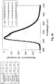
- triplet energy refers to an energy corresponding to the highest energy feature discernable in the phosphorescence spectrum of a given material.
- the highest energy feature is not necessarily the peak having the greatest intensity in the phosphorescence spectrum, and could, for example, be a local maximum of a clear shoulder on the high energy side of such a peak.
- organometallic refers to compounds which have an organic group bonded to a metal through a carbon-metal bond. This class does not include per se coordination compounds, which are substances having only donor bonds from heteroatoms, such as metal complexes of anines, halides, pseudohalides (CN, etc.), and the like. In practice organometallic compounds generally comprise, in addition to one or more carbon-metal bonds to an organic species, one or more donor bonds from a heteroatom.
- the carbon-metal bond to an organic species refers to a direct bond between a metal and a carbon atom of an organic group, such as phenyl, alkyl, alkenyl, etc., but does not refer to a metal bond to an "inorganic carbon," such as the carbon of CN.
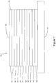
- Fig. 1 shows an organic light emitting device 100.
- Device 100 may include a substrate 110, an anode 115, a hole injection layer 120, a hole transport layer 125, an electron blocking layer 130, an emissive layer 135, a hole blocking layer 140, an electron transport layer (ETL) 145, an electron injection layer 150, a protective layer 155, and a cathode 160.
- Cathode 160 is a compound cathode having a first conductive layer 162 and a second conductive layer 164.
- Device 100 may be fabricated by depositing the layers described, in order.
- Substrate 110 may be any suitable substrate that provides desired structural properties.
- Substrate 110 may be flexible or rigid.
- Substrate 110 may be transparent, translucent or opaque.
- Plastic and glass are examples of preferred rigid substrate materials.
- Plastic and metal foils are examples of preferred flexible substrate materials.
- Substrate 110 may be a semiconductor material in order to facilitate the fabrication of circuitry.
- substrate 110 may be a silicon wafer upon which circuits are fabricated, capable of controlling OLEDs subsequently deposited on the substrate. Other substrates may be used.
- the material and thickness of substrate 110 may be chosen to obtain desired structural and optical properties.
- Anode 115 may be any suitable anode that is sufficiently conductive to transport holes to the organic layers.
- the material of anode 115 preferably has a work function higher than about 4 eV (a "high work function material").
- Preferred anode materials include conductive metal oxides, such as indium tin oxide (ITO) and indium zinc oxide (IZO), aluminum zinc oxide (AlZnO), and metals.
- Anode 115 (and substrate 110) may be sufficiently transparent to create a bottom-emitting device.
- a preferred transparent substrate and anode combination is commercially available ITO (anode) deposited on glass or plastic (substrate).
- a flexible and transparent substrate-anode combination is disclosed in United States Patent Nos.
- Anode 115 may be opaque and/or reflective. A reflective anode 115 may be preferred for some top-emitting devices, to increase the amount of light emitted from the top of the device.
- the material and thickness of anode 115 may be chosen to obtain desired conductive and optical properties. Where anode 115 is transparent, there may be a range of thickness for a particular material that is thick enough to provide the desired conductivity, yet thin enough to provide the desired degree of transparency. Other anode materials and structures may be used.
- Hole transport layer 125 may include a material capable of transporting holes.
- Hole transport layer 130 may be intrinsic (undoped), or doped. Doping may be used to enhance conductivity.
- ⁇ -NPD and TPD are examples of intrinsic hole transport layers.
- An example of a p-doped hole transport layer is m-MTDATA doped with F 4 -TCNQ at a molar ratio of 50:1, as disclosed in United States Patent Application Publication No. 2002-0071963 A1 to Forrest et al. , which is incorporated by reference in its entirety. Other hole transport layers may be used.
- Emissive layer 135 may include an organic material capable of emitting light when a current is passed between anode 115 and cathode 160.
- emissive layer 135 contains a phosphorescent emissive material, although fluorescent emissive materials may also be used. Phosphorescent materials are preferred because of the higher luminescent efficiencies associated with such materials.
- Emissive layer 135 may also comprise a host material capable of transporting electrons and / or holes, doped with an emissive material that may trap electrons, holes, and / or excitons, such that excitons relax from the emissive material via a photoemissive mechanism.
- Emissive layer 135 may comprise a single material that combines transport and emissive properties.
- emissive layer 135 may comprise other materials, such as dopants that tune the emission of the emissive material.
- Emissive layer 135 may include a plurality of emissive materials capable of, in combination, emitting a desired spectrum of light. Examples of phosphorescent emissive materials include Ir(ppy) 3 . Examples of fluorescent emissive materials include DCM and DMQA. Examples of host materials include Alq 3 , CBP and mCP. Examples of emissive and host materials are disclosed in U.S. Patent No. 6,303,238 to Thompson et al. , which is incorporated by reference in its entirety.
- Emissive material may be included in emissive layer 135 in a number of ways.
- an emissive small molecule may be incorporated into a polymer.
- an emissive small molecule may be incorporated into a polymer. This may be accomplished by several ways: by doping the small molecule into the polymer either as a separate and distinct molecular species; or by incorporating the small molecule into the backbone of the polymer, so as to form a co-polymer; or by bonding the small molecule as a pendant group on the polymer.
- Other emissive layer materials and structures may be used.
- a small molecule emissive material may be present as the core of a dendrimer.
- a ligand may be referred to as "photoactive” if it contributes directly to the photoactive properties of an organometallic emissive material.
- a "photoactive" ligand may provide, in conjunction with a metal, the energy levels from which and to which an electron moves when a photon is emitted.
- Other ligands may be referred to as "ancillary.”
- Ancillary ligands may modify the photoactive properties of the molecule, for example by shifting the energy levels of a photoactive ligand, but ancillary ligands do not directly provide the energy levels directly involved in light emission.
- a ligand that is photoactive in one molecule may be ancillary in another.
- Electron transport layer (ETL) 140 may include a material capable of transporting electrons. Electron transport layer 140 may be intrinsic (undoped), or doped. Doping may be used to enhance conductivity. Alq 3 is an example of an intrinsic electron transport layer. An example of an n-doped electron transport layer is BPhen doped with Li at a molar ratio of 1:1, as disclosed in United States Patent Application Publication No. 2002-0071963 A1 to Forrest et al. , which is incorporated by reference in its entirety. Other electron transport layers may be used.
- the charge carrying component of the electron transport layer may be selected such that electrons can be efficiently injected from the cathode into the LUMO (Lowest Unoccupied Molecular Orbital) level of the electron transport layer.
- the "charge carrying component" is the material responsible for the LUMO that actually transports electrons. This component may be the base material, or it may be a dopant.
- the LUMO level of an organic material may be generally characterized by the electron affinity of that material and the relative electron injection efficiency of a cathode may be generally characterized in terms of the work function of the cathode material. This means that the preferred properties of an electron transport layer and the adjacent cathode may be specified in terms of the electron affinity of the charge carrying component of the ETL and the work function of the cathode material.
- the work function of the cathode material is preferably not greater than the electron affinity of the charge carrying component of the electron transport layer by more than about 0.75 eV, more preferably, by not more than about 0.5 eV. Similar considerations apply to any layer into which electrons are being injected.
- Cathode 160 may be any suitable material or combination of materials known to the art, such that cathode 160 is capable of conducting electrons and injecting them into the organic layers of device 100. Cathode 160 may be transparent or opaque, and may be reflective. Metals and metal oxides are examples of suitable cathode materials. Cathode 160 may be a single layer, or may have a compound structure. Figure 1 shows a compound cathode 160 having a thin metal layer 162 and a thicker conductive metal oxide layer 164. In a compound cathode, preferred materials for the thicker layer 164 include ITO, IZO, and other materials known to the art. U.S. Patent Nos.
- cathodes including compound cathodes having a thin layer of metal such as Mg:Ag with an overlying transparent, electrically-conductive, sputter-deposited ITO layer.
- the part of cathode 160 that is in contact with the underlying organic layer, whether it is a single layer cathode 160, the thin metal layer 162 of a compound cathode, or some other part, is preferably made of a material having a work function lower than about 4 eV (a "low work function material").
- Other cathode materials and structures may be used.
- Blocking layers may be used to reduce the number of charge carriers (electrons or holes) and / or excitons that leave the emissive layer.
- An electron blocking layer 130 maybe disposed between emissive layer 135 and the hole transport layer 125, to block electrons from leaving emissive layer 135 in the direction of hole transport layer 125.
- a hole blocking layer 140 may be disposed between emissive layer135 and electron transport layer 145, to block holes from leaving emissive layer 135 in the direction of electron transport layer 140.
- Blocking layers may also be used to block excitons from diffusing out of the emissive layer. The theory and use of blocking layers is described in more detail in United States Patent No. 6,097,147 and United States Patent Application Publication No. 2002-0071963 A1 to Forrest et al. , which are incorporated by reference in their entireties.
- blocking layer means that the layer provides a barrier that significantly inhibits transport of charge carriers and/or excitons through the device, without suggesting that the layer necessarily completely blocks the charge carriers and/or excitons.
- the presence of such a blocking layer in a device may result in substantially higher efficiencies as compared to a similar device lacking a blocking layer.
- a blocking layer may be used to confine emission to a desired region of an OLED.
- injection layers are comprised of a material that may improve the injection of charge carriers from one layer, such as an electrode or an organic layer, into an adjacent organic layer. Injection layers may also perform a charge transport function.
- hole injection layer 120 may be any layer that improves the injection of holes from anode 115 into hole transport layer 125.
- CuPc is an example of a material that may be used as a hole injection layer from an ITO anode 115, and other anodes.
- electron injection layer 150 may be any layer that improves the injection of electrons into electron transport layer 145.
- LiF/Al is an example of a material that may be used as an electron injection layer into an electron transport layer from an adjacent layer. Other materials or combinations of materials may be used for injection layers.
- injection layers may be disposed at locations different than those shown in device 100. More examples of injection layers are provided in U.S. Patent Application Serial No. 09/931,948 to Lu et al. , which is incorporated by reference in its entirety.
- a hole injection layer may comprise a solution deposited material, such as a spin-coated polymer, e.g., PEDOT:PSS, or it may be a vapor deposited small molecule material, e.g., CuPc or MTDATA.
- a hole injection layer may planarize or wet the anode surface so as to provide efficient hole injection from the anode into the hole injecting material.
- a hole injection layer may also have a charge carrying component having HOMO (Highest Occupied Molecular Orbital) energy levels that favorably match up, as defined by their herein-described relative ionization potential (IP) energies, with the adjacent anode layer on one side of the HIL and the hole transporting layer on the opposite side of the HIL.
- the "charge carrying component” is the material responsible for the HOMO that actually transports holes. This component may be the base material of the HIL, or it may be a dopant.
- a doped HIL allows the dopant to be selected for its electrical properties, and the host to be selected for morphological properties such as wetting, flexibility, toughness, etc.
- Preferred properties for the HIL material are such that holes can be efficiently injected from the anode into the HIL material.
- the charge carrying component of the HIL preferably has an IP not more than about 0.7 eV greater that the IP of the anode material. More preferably, the charge carrying component has an IP not more than about 0.5 eV greater than the anode material. Similar considerations apply to any layer into which holes are being injected.
- HIL materials are further distinguished from conventional hole transporting materials that are typically used in the hole transporting layer of an OLED in that such HIL materials may have a hole conductivity that is substantially less than the hole conductivity of conventional hole transporting materials.
- the thickness of the HIL of the present invention may be thick enough to help planarize or wet the surface of the anode layer. For example, an HIL thickness of as little as 10 nm may be acceptable for a very smooth anode surface. However, since anode surfaces tend to be very rough, a thickness for the HIL of up to 50 nm may be desired in some cases.
- a protective layer may be used to protect underlying layers during subsequent fabrication processes.
- the processes used to fabricate metal or metal oxide top electrodes may damage organic layers, and a protective layer may be used to reduce or eliminate such damage.
- protective layer 155 may reduce damage to underlying organic layers during the fabrication of cathode 160.
- a protective layer has a high carrier mobility for the type of carrier that it transports (electrons in device 100), such that it does not significantly increase the operating voltage of device 100.
- CuPc, BCP, and various metal phthalocyanines are examples of materials that may be used in protective layers. Other materials or combinations of materials may be used.
- protective layer 155 is preferably thick enough that there is little or no damage to underlying layers due to fabrication processes that occur after organic protective layer 160 is deposited, yet not so thick as to significantly increase the operating voltage of device 100.
- Protective layer 155 may be doped to increase its conductivity.
- a CuPc or BCP protective layer 160 may be doped with Li.
- Figure 2 shows an inverted OLED 200.
- the device includes a substrate 210, an cathode 215, an emissive layer 220, a hole transport layer 225, and an anode 230.
- Device 200 may be fabricated by depositing the layers described, in order. Because the most common OLED configuration has a cathode disposed over the anode, and device 200 has cathode 215 disposed under anode 230, device 200 may be referred to as an "inverted" OLED. Materials similar to those described with respect to device 100 may be used in the corresponding layers of device 200. Figure 2 provides one example of how some layers may be omitted from the structure of device 100.
- the simple layered structure illustrated in Figures 1 and 2 is provided by way of non-limiting example, and it is understood that embodiments of the invention may be used in connection with a wide variety of other structures.
- the specific materials and structures described are exemplary in nature, and other materials and structures may be used.
- Functional OLEDs may be achieved by combining the various layers described in different ways, or layers may be omitted entirely, based on design, performance, and cost factors. Other layers not specifically described may also be included. Materials other than those specifically described may be used. Although many of the examples provided herein describe various layers as comprising a single material, it is understood that combinations of materials, such as a mixture of host and dopant, or more generally a mixture, may be used. Also, the layers may have various sublayers.
- hole transport layer 225 transports holes and injects holes into emissive layer 220, and may be described as a hole transport layer or a hole injection layer.
- an OLED may be described as having an "organic layer" disposed between a cathode and an anode. This organic layer may comprise a single layer, or may further comprise multiple layers of different organic materials as described, for example, with respect to Figures 1 and 2 .
- OLEDs comprised of polymeric materials (PLEDs) such as disclosed in U.S. Pat. No. 5,247,190, Friend et al. , which is incorporated by reference in its entirety.
- PLEDs polymeric materials
- OLEDs having a single organic layer may be used.
- OLEDs may be stacked, for example as described in U.S. Patent No. 5,707,745 to Forrest et al , which is incorporated by reference in its entirety.
- the OLED structure may deviate from the simple layered structure illustrated in Figures 1 and 2 .
- the substrate may include an angled reflective surface to improve out-coupling, such as a mesa structure as described in U.S. Patent No. 6,091,195 to Forrest et al. , and / or a pit structure as described in U.S. Patent No. 5,834,893 to Bulovic et al. , which are incorporated by reference in their entireties.
- any of the layers of the various embodiments may be deposited by any suitable method.
- preferred methods include thermal evaporation, ink-jet, such as described in U.S. Patent Nos. 6,013,982 and 6,087,196 , which are incorporated by reference in their entireties, organic vapor phase deposition (OVPD), such as described in U.S. Patent No. 6,337,102 to Forrest et al. , which is incorporated by reference in its entirety, and deposition by organic vapor jet printing (OVJP), such as described in U.S. Patent Application No. 10/233,470 , which is incorporated by reference in its entirety.
- OVPD organic vapor phase deposition
- OJP organic vapor jet printing
- Other suitable deposition methods include spin coating and other solution based processes.
- Solution based processes are preferably carried out in nitrogen or an inert atmosphere.
- preferred methods include thermal evaporation.
- Preferred patterning methods include deposition through a mask, cold welding such as described in U.S. Patent Nos. 6,294,398 and 6,468,819 , which are incorporated by reference in their entireties, and patterning associated with some of the deposition methods such as ink-jet and OVJD. Other methods may also be used.
- the materials to be deposited may be modified to make them compatible with a particular deposition method. For example, substituents such as alkyl and aryl groups, branched or unbranched, and preferably containing at least 3 carbons, may be used in small molecules to enhance their ability to undergo solution processing.
- Substituents having 20 carbons or more may be used, and 3-20 carbons is a preferred range. Materials with asymmetric structures may have better solution processibility than those having symmetric structures, because asymmetric materials may have a lower tendency to recrystallize. Dendrimer substituents may be used to enhance the ability of small molecules to undergo solution processing.
- substituents may be added to a compound having three bidentate ligands, such that after the substituents are added, one or more of the bidentate ligands are linked together via a linking group to form, for example, a tetradentate or hexadentate ligand having linking group that covalently links a first ligand to a second ligand.
- a linking group to form, for example, a tetradentate or hexadentate ligand having linking group that covalently links a first ligand to a second ligand.
- Other linkages may be formed. Suitable linking groups and linkages are described, for example, in U.S. Patent Application Serial No2. 10/771,423 and 10/859,796 which are incorporated by reference herein in their entireties.
- the multidentate ligand systems are prepared by the metal catalyzed coupling of the linking group to the ligand. See, for example, Beeston et al., Inorg. Chem. 1998, 37, 4368-4379 .
- the linking group X provides no ⁇ -conjugation between the linked ligands. Having ⁇ -conjugation between the linked ligands may change the electronic properties of the ligands and the resulting metal complexes, such as a red-shift in the luminescence.
- a non-conjugated linking group may comprise at least one atom in the linkage which contains no ⁇ -electrons, such as an sp 3 hybridized carbon or silicon.
- the linking group in a preferred embodiment of the invention, the linking group,
- X is selected from the group consisting of -(CR 2 ) d -, -[O(CR 2 ) e ]O-, or a group having the formula or
- Devices fabricated in accordance with embodiments of the invention may be incorporated into a wide variety of consumer products, including flat panel displays, computer monitors, televisions, billboards, lights for interior or exterior illumination and/or signaling, heads up displays, fully transparent displays, flexible displays, laser printers, telephones, cell phones, personal digital assistants (PDAs), laptop computers, digital cameras, camcorders, viewfinders, micro-displays, vehicles, a large area wall, theater or stadium screen, or a sign.
- PDAs personal digital assistants
- Various control mechanisms may be used to control devices fabricated in accordance with the present invention, including passive matrix and active matrix. Many of the devices are intended for use in a temperature range comfortable to humans, such as 18 degrees C to 30 degrees C, and more preferably at room temperature (20 - 25 degrees C).
- the materials and structures described herein may have applications in devices other than OLEDs.
- other optoelectronic devices such as organic solar cells and organic photodetectors may employ the materials and structures.
- organic devices such as organic transistors, may employ the materials and structures.
- halo or halogen as used herein includes fluorine, chlorine, bromine and iodine.
- alkyl as used herein contemplates both straight and branched chain alkyl radicals.
- Preferred alkyl groups are those containing from one to fifteen carbon atoms and includes methyl, ethyl, propyl, isopropyl, butyl, isobutyl, tert -butyl, and the like. Additionally, the alkyl group may be optionally substituted with one or more substituents selected from halo, CN, CO 2 R, C(O)R, NR 2 , cyclic-amino, NO 2 , and OR.
- cycloalkyl as used herein contemplates cyclic alkyl radicals.
- Preferred cycloalkyl groups are those containing 3 to 7 carbon atoms and includes cyclopropyl, cyclopentyl, cyclohexyl, and the like. Additionally, the cycloalkyl group may be optionally substituted with one or more substituents selected from halo, CN, CO 2 R, C(O)R, NR 2 , cyclic-amino, NO 2 , and OR.
- alkenyl as used herein contemplates both straight and branched chain alkene radicals. Preferred alkenyl groups are those containing two to fifteen carbon atoms. Additionally, the alkenyl group may be optionally substituted with one or more substituents selected from halo, CN, CO 2 R, C(O)R, NR 2 , cyclic-amino, NO 2 , and OR.
- alkynyl as used herein contemplates both straight and branched chain alkyne radicals. Preferred alkyl groups are those containing two to fifteen carbon atoms. Additionally, the alkynyl group may be optionally substituted with one or more substituents selected from halo, CN, CO 2 R, C(O)R, NR 2 , cyclic-amino, NO 2 , and OR.
- alkylaryl as used herein contemplates an alkyl group that has as a substituent an aromatic group. Additionally, the alkylaryl group may be optionally substituted on the aryl with one or more substituents selected from halo, CN, CO 2 R, C(O)R, NR 2 , cyclic-amino, NO 2 , and OR.
- substituents selected from halo, CN, CO 2 R, C(O)R, NR 2 , cyclic-amino, NO 2 , and OR.
- heterocyclic group as used herein contemplates non-aromatic cyclic radicals.
- Preferred heterocyclic groups are those containing 3 or 7 ring atoms which includes at least one hetero atom, and includes cyclic amines such as morpholino, piperdino, pyrrolidino, and the like, and cyclic ethers, such as tetrahydrofuran, tetrahydropyran, and the like.
- aryl or aromatic group contemplates single-ring groups and polycyclic ring systems.
- the polycyclic rings may have two or more rings in which two carbons are common by two adjoining rings (the rings are "fused") wherein at least one of the rings is aromatic, e.g., the other rings can be cycloalkyls, cycloalkenyls, aryl, heterocycles and/or heteroaryls.
- heteroaryl as used herein contemplates single-ring hetero-aromatic groups that may include from one to three heteroatoms, for example, pyrrole, furan, thiophene, imidazole, oxazole, thiazole, triazole, pyrazole, pyridine, pyrazine and pyrimidine, and the like.
- heteroaryl also includes polycyclic hetero-aromatic systems having two or more rings in which two atoms are common to two adjoining rings (the rings are "fused") wherein at least one of the rings is a heteroaryl, e.g., the other rings can be cycloalkyls, cycloalkenyls, aryl, heterocycles and/or heteroaryls.
- the phosphorescent dopants used are Ir( 5'-alkyl-2-phenylpyridine) type metal complexes. Many alkyl substituted on Ir(2-phenylpyridine) complexes are known. However, we have found that 5'-alkyl substituted analogs have unexpected properties such that, when they are incorporated into an organic light emitting device, unexpected results are attained. In some embodiments, the phosphorescent dopants used are Ir(5'-alkyl substituted phenyl-isoquinoline) type metal complexes. By incorporating the phosphorescent materials of the present invention into organic light emitting devices (OLEDs), unexpected and exceptionally high device efficiencies have been demonstrated.
- OLEDs organic light emitting devices
- a phosphorescent emissive material having improved efficiency when incorporated into an organic light emitting device is provided, the emissive material having the formula I
- n is the maximum number of ligands that may be attached to the metal.
- the emissive material comprises at least one photoactive ligand and a heavy metal ion such that the resulting material has (i) a carbon-metal bond between ring B and the metal and (ii) the nitrogen of ring A is coordinated to the metal.
- the emissive materials of Formula I comprise a partial structure having the following formula
- M may be Ir, Pt, Rh or Pd.
- the metal is Ir or Pt. Most preferably, the metal is Ir.
- the number of photoactive ligands of a particular type may be any integer from 1 to the maximum number of ligands that may be attached to the metal.
- m may be 1, 2 or 3.
- n the number of "ancillary" ligands of a particular type, may be any integer from zero to one less than the maximum number of ligands that may be attached to the metal.
- (X-Y) represents an ancillary ligand.
- n may be 0, 1 or 2 for bidentate ligands.
- Ancillary ligands for use in the emissive material may be selected from those known in the art.
- Non-limiting examples of ancillary ligands may be found in PCT Application Publication WO 02/15645 A1 to Lamansky et al. at pages 89-90, which is incorporated herein by reference.
- Preferred ancillary ligands include acetylacetonate (acac) and picolinate (pic), and derivatives thereof.
- the preferred ancillary ligands have the following structures:
- the emissive materials of Formula I include an emissive material having a formula where n is zero and m is the maximum number of ligands that may be attached to the metal as depicted in the following structure:
- m is three in this preferred embodiment, and the structure may be referred to as a "tris" structure.
- the tris structure is preferred because it is believed to be particularly stable.
- R 3 , R 4 , R 5 , R 6 R' 3 , R' 4 , R' 5 and R' 6 are defined according to the definitions of Formula I.
- m + n is equal to the total number of bidentate ligands that may be attached to the metal in question -- for example, 3 for Ir. In another embodiment, m + n may be less than the maximum number of bidentate ligands that may be attached to the metal, in which case other ligands -- ancillary, photoactive, or otherwise -- may also be attached to the metal.
- M is Ir and m is 3, giving an emissive material of the formula:
- R 3 , R 4 , R 5 , R 6 , R' 3 , R' 4 , R' 5 and R' 6 are defined according to the definitions of Formula I.
- ring A is pyridyl.
- substituents at R' 3 and R' 4 form a fused ring.
- An example of a red emitting embodiment of the present invention includes an emissive material of Formula I having the following structure:
- M may be Ir, Pt, Rh or Pd.
- the metal is Ir or Pt.
- the metal is Ir.
- This embodiment includes an emissive material wherein M is iridium and R' 5 is methyl having the structural formula:
- M is iridium and R' 5 is methyl
- R' 5 is methyl
- R 3 , R 4 , R 5 , R 6 R' 3 , R' 4 , and R' 6 is a phenyl substituent.
- This embodiment includes an emissive material of Formula I where n is zero, and m is the maximum number of ligands that may be attached to the metal as depicted in the following structures:
- m is three in this preferred embodiment, and the structure may be referred to as a "tris" structure.
- the tris structure is preferred because it is believed to be particularly stable.
- R 3 , R 4 , R 5 , R 6 , R' 3, , R' 4 , R' 5 , and R' 6 are defined according to the definitions of Formula I.
- m + n is equal to the total number of bidentate ligands that may be attached to the metal in question -- for example, 3 for Ir. In another embodiment, m + n may be less than the maximum number of bidentate ligands that may be attached to the metal, in which case other ligands -- ancillary, photoactive, or otherwise -- may also be attached to the metal.
- ring A is a non-fused pyridyl ring, at least one of R 3 , R 4 , R 5 , R 6 , R' 3 , R' 4 , and R' 6 comprises a phenyl moiety.
- at least one of R 4 , R 5 , R 6 is an unsubstituted phenyl ring, a fluoro-substituted phenyl ring or a phenyl ring substituted with a substituent that renders the phenyl ring equally or less coplanar than the unsubstituted phenyl ring with respect to Ring B.
- the substituent that renders the phenyl ring equally or less coplanar than the unsubstituted phenyl ring with respect to Ring B is an alkyl substituent.
- This embodiment includes an emissive material having the formula or
- R 7 is H, F or a substituent that renders the phenyl substituent at Ring B equally coplanar with or less coplanar than the unsubstituted phenyl ring with respect to Ring B.
- R 7 is selected from the group consisting of H, F and alkyl---These emissive materials include a ligand structure of the formula
- R' 5 is methyl and m is 3, giving an emissive material of the formula:
- R 5 is unsubstituted phenyl, giving an emissive material of the formula with a ligand structure having the formula: and a partial structure for the emissive material of the formula:
- R 3 , R 4 , R 6 , R' 3 R' 4 , R' 5 , and R' 6 are defined according to the definitions of Formula I.
- R 5 is unsubstituted phenyl
- M is Ir and m is 3, giving an emissive material of the formula:
- R 3 , R 4 , R 6 , R' 3 R' 4 , R' 5 , and R' 6 are defined according to the definitions of Formula I.
- R' 5 is methyl
- R 5 is unsubstituted phenyl
- the emissive material of this embodiment has the following structure:
- R' 5 is methyl, m is 3, M is Ir and R 5 is alkyl-substituted phenyl, preferably methyl-substituted phenyl giving an emissive material of the formula:
- R' 5 is methyl, m is 3, M is Ir and R 5 is fluoro- substituted phenyl giving an emissive material of the formula:
- n is zero
- m is the maximum number of ligands that may be attached to the metal.
- m is three in this preferred embodiment, and the structure may be referred to as a "tris" structure.
- the tris structure is preferred because it is believed to be particularly stable.
- R 5' is alkyl as defined in Formula I.
- m + n is equal to the total number of bidentate ligands that may be attached to the metal in question - for example, 3 for Ir. In another embodiment, m + n may be less than the maximum number of bidentate ligands that may be attached to the metal, in which case other ligands-ancillary, photoactive, or otherwise - may also be attached to the metal. Preferably, if there are different photoactive ligands attached to the metal, each photoactive ligand has the structure indicated in Formula I.
- M is Ir and m is 3, giving an emissive material of the formula:
- R 5' is alkyl as defined in Formula I.
- R' 5 is methyl.
- the emissive material of this embodiment has the following structure: and comprises a ligand having the following structure and a partial structure of for the emissive material as follows:
- At least one of R' 3 , R' 4 and R' 6 is alkyl in addition to R' 5 being alkyl. In such an embodiment, the remaining positions can be optionally substituted according to the definitions of Formula I.
- This embodiment includes emissive materials in which at least one of R' 3 , R' 4 and R' 6 is methyl as depicted in the following structural formulas having corresponding ligand structures as depicted respectively below: and having partial structures for the emissive material comprising ligand structures of depicted respectively below:
- n is zero
- m is the maximum number of ligands that may be attached to the metal as depicted in the structures below:
- This embodiment of the invention includes, for example, molecules with the following structures where M is Ir and m is 3, and R' 5 is methyl:
- Another embodiment of the invention comprises an emissive material having a formula in which at least one of R' 3 , R' 4 , and R' 6 is alkyl and at least one of R 3 , R 4 , R 5 and R 6 is aryl, preferably phenyl or substituted phenyl.
- R 5 is a phenyl substituent and at least one of R' 3 , R' 4 , and R' 6 is a methyl substituent.
- R 5 is phenyl and R' 4 is methyl.
- R 5 is phenyl and R' 3 is methyl.
- R 5 is phenyl and R' 6 is methyl.
- an emissive material comprising a molecule with one of the following formulas: each having a corresponding ligand structure as depicted, respectively, below: and partial structures for the emissive material as depicted, respectively, below:
- n is zero
- m is the maximum number of ligands that may be attached to the metal.
- n is zero
- m is the maximum number of ligands that may be attached to the metal.
- the emissive materials comprises a molecule having a formula where M is Ir and m is 3 as depicted below:
- R 5' is defined according to the definitions of Formula I.
- R' 5 is methyl giving an emissive material of the formula:
- the light emitting devices of the present invention may exhibit an operational half-life in excess of about 50 hours, or preferably 100 hours, or even more preferably 200 hours at initial luminance of about 10,700 cd/m 2 or preferably 12,000 cd/m 2 , or even more preferably 16,000 cd/m 2 or most preferably 17,000 cd/m 2 .
- substitution at the R' 3 position to increase device lifetime as disclosed in United States Patent Application No. 10/765,295 to Kwong et al. which is incorporated by reference herein in its entirety.
- substitution at the R 5 position has also been shown to increase device lifetime, as disclosed in United States Patent Application No. 10/289,915 to Brown et al. , which is also incorporated by reference in its entirety.
- alkyl substitution at the R' 5 position shows exceptional efficiency in particular devices.
- Substitution at the R 5 in addition to alkyl substitution R' 5 position may show a further improvement in efficiency over alkyl substitution at only the R' 5 position.
- specific substituents shown in Formula I provide a particularly efficient molecule, when R 5 is phenyl and R' 5 is methyl, both un-substituted. It is further believed that the enhanced efficiency is still present if the phenyl and/or methyl in the R 5 and R' 5 positions, respectively, are substituted.
- the term “external quantum efficiency” refers to the percentage of charge carriers injected into a device that result in the emission of a photon from the device in the forward direction. A number of factors can affect the external quantum efficiency, including the "internal quantum efficiency,” which is the percentage of charge carriers injected into a device that result in the creation of a photon, and the “outcoupling efficiency,” which is the percentage of photons created that are emitted from a device towards a viewer.
- an organic layer comprising a 5'alkyl substituted dopant (with and without an aromatic hydrocarbon layer (HPT) that is in direct contact with an emissive layer) may enhance the internal quantum efficiency and thus the external quantum efficiency of the device.
- external quantum efficiency is more readily and directly measured than internal quantum efficiency, it may be desirable to describe certain aspects of the invention with respect to external quantum efficiency. But, in order to determine whether an enhanced external quantum efficiency is due to the use of an alkyl substituent at position 5', it is preferable to account for other factors that affect external quantum efficiency.
- the term "unmodified external quantum efficiency" as used herein refers to the external quantum efficiency of a device, after multiplication by a factor to account for any differences in the outcoupling efficiency of that device and the outcoupling efficiency of the devices described experimentally herein.
- a typical outcoupling efficiency for the types of devices described herein is about 20-30%.
- Stability may be measured in a number of ways.
- One stability measurement is the operational stability of the electroluminescent device which can be measured in terms of operational half-life.
- the operational half-life is the time required for the luminance of the device to decay from the initial luminance (L 0 ) to 50% of its initial luminance (L 0.5 ) under constant current and at room temperature unless otherwise noted. Operational half-life depends upon luminance at which the device is operated, because a higher luminance generally corresponds to a faster decay in a particular device. Luminance may be measured in cd/m 2 .
- Devices in accordance with embodiments of the present invention can advantageously have an operational half-life in excess of about 50 hours, preferably about 100 hours, more preferably about 200 hours at initial luminance of about 10,700 cd/m 2 preferably about 12,000 cd/m 2 , more preferably about 16,000 cd/m 2 , most preferably about 17,000 cd/m 2 or higher.
- the emissive material of the present invention may comprise a compound of Formula I such that the device has an unmodified external quantum efficiency of at least about 10% at current densities between about 0.1 to about 1000 mA/cm 2 ; and a lifetime of at least about 50 hours at an initial luminance of at least about 10700 cd/m 2 .
- the emissive material may comprise a compound of Formula I such that the device has an unmodified external quantum efficiency of at least about 15%, preferably at least about 20 % at current densities from about 0.1 to about 1000 mA/cm 2 ; and a lifetime of at least about 50 hours at an initial luminance of at least about 10,700 cd/m 2 .
- the emissive layer may be in direct contact with an electron transport layer comprising a material having a molecular dipole moment less than about 2.0 debyes, such that the device has an external quantum efficiency of at least about 10% at about at current densities between about 0.1 to about 1000 mA/cm 2 .
- a second electron transport layer including an aromatic hydrocarbon having a zero or low molecular dipole moment (TPD) adjacent to the emissive layer may further enhance device performance, as disclosed in U.S. patent application serial number 10/785, 287 which is incorporated by reference in its entirety herein. Without intending to limit all embodiments with a particular theory of how the invention works, it is believed that this symmetric energy structure may improve electron injection from ETL2 into the emissive layer.
- the (ETL2) maybe in direct contact with the cathode, or there may be a separate organic layer between the organic enhancement layer and the cathode. Other aromatic hydrocarbon materials may be used.
- alkyl and aryl substitutions offer a wide range of tunability in terms of evaporation temperature, solubility, energy levels, device efficiency, and are stable functional groups chemically and in device operation.
- alkyl groups i.e., by appropriately substituting one or more alkyl groups (i.e., by appropriately substituting one or more alkyl groups (i.e., by appropriately substituting one or more alkyl groups (i.e., by appropriately substituting one or more alkyl groups (i.e.
- dopant emitters for OLED devices
- the properties observed gave unexpected improvements in material and device properties including sublimability (lower depositions temperatures and remaining residue in the boat), solubility, color tunability, device stability, and device efficiencies.
- the color of emission can be fine-tuned to give greater saturation and more desired CIE color requirements.
- alkyl and aryl substituted emissive materials of the invention have chemical structures as follows: Compound Structure XIV XV XVI XVII XVIII XIX XX XI XXII XXIII XXIV XXV XVI XXVII XXVIII XXIX XXXXI
- 2-(3-bromophenyl)-5-methylpyridine (14.0 g, 61 mmol), phenylboronic acid (8.8 g, 72 mmol), palladium (II) acetate (0.34 g, 1.5 mmol), triphenylphosphine (1.6 g, 6.1 mmol), and potassium carbonate (22.3 g, 162 mmol) were mixed with 120 mL of ethylene glycol dimethyl ether and 80 mL of water in a 500 mL round bottom flask equipped with a temperature probe, reflux condenser, and a magnetic stir bar. The solution was then heated at reflux under nitrogen for 16 hr.
- Step 3 Synthesis of tris[2-(biphenyl-3-yl)-5-methylpyridine-N,C 2' ]iridium (III).
- COMPOUND III Comparative Example Compound, tris(2-[3-biphenyl]pyridine)Iridium (III): [Ir(5-Phppy) 3 ] Synthesis
- COMPOUND IV fac tris[1-phenyl-4-methylisoquinolinolato-N,C 2' ] iridium(III) [Ir(4-Me-1-piq) 3 ] Synthesis
- Step 4 Synthesis of Bis[1-phenyl-4-methylisoquinolinato-N,C2']iridium (III) ⁇ -dichloro-bridged dimer.
- Step 5 Bis(1-phenyl-4-methylisoquinolinato-N,C2')iridium (III) acetylacetonate:
- Step 6 tris[1-phenyl-4-methylisoquinolinolato-N,C2'] iridium(III).
- COMPOUND V fac tris[3-methyl-5,6 dihydrobenzo [h] quinolinato-N,C 2' ] iridium(III) [Ir(3-Me-dhbq) 3 ] Synthesis
- Step 4 fac tris[3-methyl-5,6-dihydrobenzo[h]quinolinato-N,C 2' ] iridium(III)
- Step 4 fac tris[2-(2'-methylbiphenyl-3-yl)pyridinato-N,C 2' ] iridium(III)
- 2-(4-Bromophenyl)-5-methylpyridine (9.3 g, 0.038 mol.) was added to a mixture of dry toluene (70 mL), dry diisopropylamine (70 mL), 1,3,5-triethynylbenzene (2.0 g, 0.0133 mol), palladium(0)tetrakistriphenylphosphine (1.4 g, 0.0012 mol), CuI (0.15 g) were added in a dry three-necked reaction flask. The mixture was stirred under nitrogen at room temperature for 3 hours, and then heated up to 60°C for 2 days.
- Step 3 fac tris[2-(4'-fluorobiphenyl-3-yl)-5-methylpyridine] iridium(III)
- Step 3 fac tris[2-(3'-fluorobiphenyl-3-yl)pyridine] iridium(III)
- dimer 8.5 g, 5.7 mmol
- silver triflate 2.9 g, 11.3 mmol
- 2-(3'-fluorobiphenyl-3-yl)pyridine 5.9 g, 22.5 mmol
- 2-ethoxyethanol 150 mL.
- COMPOUND X fac tris[2-(2'-fluorobiphenyl-3-yl)pyridine] iridium(III)
- Step 2 fac tris[2(2'-fluorobiphenyl-3-yl)pyridine] iridium(III)
- COMPOUND XI fac tris[2-(2',3'-difluorobiphenyl-3-yl)pyridine] iridium(III)
- COMPOUND XII fac tris[2-(2',4'-difluorobiphenyl-3-yl)pyridine] iridium(III)
- COMPOUND XIII fac tris[2-(2',5'-difluorobiphenyl-3-yl)pyridine] iridium(III)
- All devices are fabricated by high vacuum ( ⁇ 10 -7 Torr) thermal evaporation.
- the anode electrode is ⁇ 1200 ⁇ of indium tin oxide (ITO).
- the cathode consists of 10 ⁇ of LiF followed by 1,000 ⁇ of Al. All devices are encapsulated with a glass lid sealed with an epoxy resin in a nitrogen glove box ( ⁇ 1 ppm of H 2 O and O 2 ) immediately after fabrication, and a moisture getter was incorporated inside the package. Operational lifetests are performed at constant direct current at room temperature.
- the organic stack was fabricated to consist of, sequentially from the ITO surface, CuPc as a hole injection layer (HIL) at a thickness of 100 ⁇ , NPD as a hole transport layer (HTL) at a thickness of 300 ⁇ ; CBP doped with 6-12 wt% of the dopant emitter (invention compounds and comparative compounds) as the emissive layer at a thickness of 300 ⁇ .
- Adjacent to the emissive layer was an electron transport layer (ETL2) consisting of 50 or 100 ⁇ of HPT (Devices 2, 4, 6, 8, 10 and Comparative Example Device 2) or 100 ⁇ of BAlq (Devices 1, 3, 5, 7, 9 and Comparative Example Device 1).
- Adjacent to layer ETL2 was another electron transport layer (ETL1) consisting of Alq 3 at a thickness of 400 or 450 ⁇ .
- Table 2 shows the operational stability of the devices using the 5'-alkyl substituted invention compounds compared to the devices using Ir(5-Phppy) 3 which has no 5'-alkyl group (Comparative Example Device 1).
- Comparative Example Device 1 When scaled to display operation brightness (L 0 ⁇ 300 cd/m 2 for red emitting devices and 600 cd/m 2 for green emitting devices) the operational half life of Comparative Example Device 1 (a green emitting device) is at least 10,000 hours (as disclosed in U.S. Application Publication No. 2004/0086743 which is incorporated by reference herein in its entirety).
- the devices in accordance with embodiments of the present invention can advantageously have an operational half-life in excess of about 10,000 hours. It is believed, therefore, the invention compounds have advantageously very high device efficiency and long operational lifetimes.
- devices comprising the present invention compounds have superior properties as compared with known devices. While those devices exemplified in Experimental Devices 1-10 herein are green emitting devices comprising phenylpyridine type ligands, devices of the present invention can emit at any color. For example, phenylisoquinoline ligands can be coordinated to a metal atom for use in red-emitting devices as disclosed in U.S. Publication No. 2003/0072964 and US. Application Serial No. 10/829/011 , incorporated herein by reference in their entireties. When the substituents taught herein are incorporated into the emissive material of these devices, it is expected they will similarly exhibit high external quantum and luminous efficiencies and long lifetimes.
- the present invention encompasses methods of increasing device efficiency, such as can be measured for a device comprising a compound of the present invention, relative to that from a device comprising a reference compound having the same structure, but without the substituents at the substitution site(s) disclosed herein.
- Experimental Devices 11-26, and 29-40 were fabricated similarly to the Experimental Devices 1-10.
- Experimental Devices 27 and 28 and Comparative Example Devices 3 and 4 were also similarly fabricated except their emissive layers consisted of a neat layer of emissive material Ir[5'-Me-5-(2-MePh)ppy] 3 for Experimental Devices 27 and 28 and Ir(3'-Meppy) 3 for Comparative Example Devices Device 3 and 4.
- the luminous efficiency and external quantum efficiency of Experimental Devices 11-40 and Comparative Example Devices 3 and 4 were measured and are summarized in Table 3.
- Example Device3 Ir(3'-Meppy) 3 100 BAlq (100 ⁇ ) Alq 3 (400 ⁇ ) 1.8 0.6
- Example Device4 Ir(3'-Meppy) 3 100 HPT (50 ⁇ ) Alq 3 (450 ⁇ ) 8.8 2.5 29 Ir[5'-Me-5-(4-FPh)ppy] 3 VIII 6 BAlq (100 ⁇ ) Alq 3 (400 ⁇ ) 42 11.6 30 Ir[5'-Me-5-(4-FPh)ppy] 3 VIII 6 HPT (50 ⁇ ) Alq 3 (450 ⁇ ) 42 11.6 31 Ir[5'-Me-5-(4-FPh)ppy] 3 VIII 8 BAlq (100 ⁇ ) Alq 3 (400 ⁇ ) 45 12.4 32 Ir[5'-Me-5-(4-FPh)ppy] 3 VIII 8 HPT (50 ⁇ ) Alq 3 (450 ⁇ ) 53 14.6 33 Ir[5'-Me-5-(4-FPh)ppy] 3 VIII 10
- the phosphorescent light emitting devices fabricated according to the present invention showed very high external quantum efficiency.
- the voltage is also low (typically ⁇ 9 V at 10 mA/cm2) for devices having HPT ETL2.
- the voltage is about 9.5-10 V for the same device architecture (Comparative Example Device 2).
- the driving voltages of the devices with the invention compounds are about 1 to 1.5 V lower than the devices with previously known analogs having no alkyl substitution at the 5' position. These low driving voltages further increase the power efficiency of the devices
- the invention compounds also evaporate at mild temperatures. Lower evaporation temperatures can reduce damage due to thermal degradation under prolonged heating during OLED manufacturing by thermal vacuum deposition or other deposition processes that require vapor transport of the materials.
- the evaporated temperature of organic materials used in OLEDs is an important aspect in OLED manufacturing.
- the evaporation temperature is the deposition temperature at a deposition rate of ⁇ 0.2 ⁇ /s at the substrate under a vacuum of ⁇ 10 -7 torr where the source and the substrate distance is about 50 cm.
- Ir(3-Me-dhbq) 3 (Compound Example V)
- Ir[5'-Me-5-(2-MePh)ppy] 3 Compound Example VI
- the hexadentate ligand complex (Compound Example VII) evaporate at ⁇ 235°C, ⁇ 265°C and ⁇ 270°C respectively. These temperatures are lower than that of Ir(5-Phppy) 3 (Comparative Example Compound III) which evaporates at ⁇ 300°C under the same conditions.
- Modifications to the 5'alkyl substituted ligands of the present invention including further substitutions with certain substituents may further lower the evaporation temperature of the complexes.
- Table 4 where the phenyl substituent at the 5 position is designated ring "C"
- invention compounds Ir(5'-Me-5-Phppy) 3 (Compound Example No. II), Ir[5'-Me-5-(2-MePh)ppy] 3 (Compound Example No. VII), Ir[5'-Me-5-(4-FPh)ppy] 3 (Compound Example No. VIII) and Ir[5'-Me-5-(3-FPh)ppy] 3 (Compound Example No.
- phenyl ring C may have substituents that cause ring C to be equally or less co-planar with respect to ring B than when ring C is un-substituted.
- Substituents on ring C that cause rings B and C to be more co-planar, especially substituents resulting in dihedral angles less than 20° may be less desirable. It is expected that compounds where ring C has bridging substituents such as (which have dihedral angles between rings B and C of about 0°) would not lower evaporation temperatures over the compounds where ring C is unsubstituted due to increased molecular packing when the phenyl rings are coplanar. Thus, preferred substituents are those that result in a dihedral angle between Rings B and C of at least 20°, more preferably at least 45° and most preferably greater than 45°.
- Examples VIII and IX exhibit evaporation temperatures that are 35°C lower than that of Example II. While the dihedral angles between Rings B and C are similar for Examples II, VIII and IV (48°), it is believed that fluorine-containing substituents such as those in Examples VIII and IX can lower the degree of molecular packing in the solid state, hence lowering evaporation temperature in organic materials because fluoro groups have weak van der Waals interactions with regular organic groups. Therefore, fluorine containing substituents are desirable groups to lower the evaporation temperature.
- conjugated substituents on Ring C may not be desirable.
- Conjugated substituents such as a fused benzene or other fused aromatic ring, tend to delocalize the electrons in the ligand and lead to a lower triplet energy for the organometallic complex (resulting in a red-shift in the phosphorescence).
- Fused benzene or other aromatic ring substituent on ring C is also believed to increase the evaporation temperature as the fused rings may induce additional molecular packing of the compounds in the solid state.
- substituents on Ring C are non-conjugated substituents that do not cause electron delocalization and those that result in increased non-coplanarity between Rings B and C relative to the degree of coplanarity when Ring C (for example, phenyl) is unsubstituted.
- 2-bromophenylboronic acid (35.0 g, 0.174 mol) was reacted with 2-bromopyridine (55.1 g, 0.348 mol) under standard Suzuki coupling condition.
- the excess 2-bromopyridine was removed via vacuum distillation at 125°C.
- the product was collected at 180°C as a light yellow liquid (29 g, 71%) and used for the next reaction without additional purification.
- Ethylene glycol (40 mL) and 2-(2'-methylbiphenyl-3-yl)pyridine (7.7 g, 31.4 mmol) were combinded in a 100 mL, three-necked flask equipped with a stir bar, reflux condenser, and a nitrogen inlet and heated to reflux.
- Ir(acac) 3 (3.8 g, 7.8 mmol) was then added and the reaction mixture was maintained at reflux for 24 hours and cooled to room temperature.
- Step 2 2-(4'- tert -butylbiphenyl-3-yl)pyridine
- Step 1 2-amino-4,5-dimethylpyridine and 2-amino-3,4-dimethylpyridine
- Step 2 2-bromo-4,5-dimethylpyridine and 2-bromo-3,4-dimethylpyridine
- Step 3 2-phenyl-4,5-dimethylpyridine and 2-phenyl-3,4-dimethylpyridine
- Step 2 mixture 12.0 g (0.0645 mol) of the Step 2 mixture was added to 9.1 g (0.071 mol) of phenylboronic acid, 2.2 g (0.002mol) of Pd(Ph 3 ) 4 , 24 g (0.174 mol) of K 2 CO 3 , 100 mL of DME and 100 mL of water.
- the reaction mixture was refluxed for 20 hours and separated on silica gel column with 10% ethyl acetate in hexane. ⁇ 7.5 g of 2-phenyl-3,4-dimethylpyridine and 2.5 g of 2-phenyl-4,5-dimethylpyridine were obtained which are confirmed by NMR and MS.
- Step 4 fac -tris(2-phenyl-4,5-dimethylpyridine) Ir(III) and fac -tris(2-phenyl-3,4-dimethylpyridine) Ir(III)
- reaction mixture was separated on silica gel column to obtain tris(2-phenyl-3,4-dimethylpyridine) Ir(III) complex as Compound XX.
- the complex was further purified by zone sublimation method and confirmed by both MS and NMR.
- Step 3 2-(biphenyl-3-yl)-4- tert -butylpyridine
- Phenylboronic acid (42.6 g, 0.349 mol) was reacted with 2-bromo-6-methylpyridine (50.0 g, 0.290 mol) under standard Suzuki coupling condition. Vacuum distillation of the product (10 mm Hg, 135-150 °C) afforded 32.0 g (76 %) of 2-(4-methylphenyl)-5-methylpyridine as a colorless liquid.
- All devices were fabricated by high vacuum ( ⁇ 10 -7 Torr) thermal evaporation.
- the anode electrode is ⁇ 1200 ⁇ of indium tin oxide (ITO).
- the cathode consists of 10 ⁇ of LiF followed by 1,000 ⁇ of Al. All devices are encapsulated with a glass lid sealed with an epoxy resin in a nitrogen glove box ( ⁇ 1 ppm of H 2 O and O 2 ) immediately after fabrication, and a moisture getter was incorporated inside the package.
- the organic stack consisted of sequentially, from the ITO surface, 100 ⁇ thick of copper phthalocyanine (CuPc) as the hole injection layer (HIL), 300 ⁇ of 4,4'-bis[N-(1-naphthyl)-N-phenylamino]biphenyl ( ⁇ -NPD), as the hole transporting layer (HTL), 300 ⁇ of 4,4'-bis(N-carbazolyl)biphenyl (CBP) doped with 6-12 wt% of the dopant emitter (invention compounds and comparative compounds) as the emissive layer (EML), 50 ⁇ of HPT as the ETL2, and 400 ⁇ of tris(8-hydroxyquinolinato)aluminum (Alq 3 ) as the ETL1.
- HIL hole injection layer
- ⁇ -NPD 4,4'-bis[N-(1-naphthyl)-N-phenylamino]biphenyl
- HTL hole transporting layer
- the current-voltage-luminance (IVL) characteristics and operational lifetimes are measured and summarized in the Table 5.
- a typical display brightness level of 1000 cd/m 2 for green emitting devices is chosen for the comparison between different devices.
- Table 5 At 1000 cd/m 2 At 40 mA/cm 2 Device Structure Device Structure T sub (°C) ⁇ max (nm) CIE Luminous efficiency (cd/A) Voltage (V) Power efficiency (lm/W) T 1/2 (hr) cd ⁇ hr/m 2 (x million) Comparative Example Device 5 6% 310 518 0.31 0.64 38.3 8.2 14.7 500 5.34 Ir(5-Phppy) 3 Comparative Example Device 6 8% 218 522 0.32 0.62 35.1 7.9 14.0 560 5.45 Ir(3'-Meppy) 3 41 6% 265-275 518 0.30 0.64 29.4 9 10.2 232 2.09 Compound XIV 42 6% 340 526 0.33 0.63 25.2 9.3 8.5 276
- Device Example 48 shows an efficiency of 36.4 cd/A at 1000 cd/m 2 and a device stability of 6.43x10 7 cd ⁇ hr/m 2 [defined as T 1/2 (hr)xL 0 (cd/m 2 ) where T 1/2 is the time for the initial luminance L 0 to drop to 50%] under a constant current drive of 40 mA/cm 2 at room temperature.
- Ir(5-Phppy) 3 (Comparative Example 5) is 38.3 cd/A and 5.34x10 7 cd ⁇ hr/m 2
- Ir(3'Meppy) 3 (Comparative Example 6) is 35.1 cd/A and 5.45x10 7 cd ⁇ hr/m 2 .
- the present invention is described with respect to particular examples and preferred embodiments, it is understood that the present invention is not limited to these examples and embodiments.
- the phosphorescent materials may contain stereo and/or structural isomers.
- the phosphorescent materials can also be of heteroleptic nature, i.e., a metal complex ligating to more than one type of ligand.
- the present invention as claimed therefore includes variations from the particular examples and preferred embodiments described herein and set forth below, as will be apparent to one of skill in the art.
- the present invention also pertains to the following numbered items:
Landscapes
- Chemical & Material Sciences (AREA)
- Organic Chemistry (AREA)
- Engineering & Computer Science (AREA)
- Materials Engineering (AREA)
- Crystallography & Structural Chemistry (AREA)
- Inorganic Chemistry (AREA)
- Physics & Mathematics (AREA)
- Optics & Photonics (AREA)
- Electroluminescent Light Sources (AREA)
- Other In-Based Heterocyclic Compounds (AREA)
- Pyridine Compounds (AREA)
Priority Applications (1)
| Application Number | Priority Date | Filing Date | Title |
|---|---|---|---|
| EP20217507.1A EP3855519A3 (de) | 2004-07-07 | 2005-07-07 | Stabile und leistungsstarke elektrolumineszente materialien |
Applications Claiming Priority (5)
| Application Number | Priority Date | Filing Date | Title |
|---|---|---|---|
| US10/886,367 US20060008671A1 (en) | 2004-07-07 | 2004-07-07 | Electroluminescent efficiency |
| US11/018,453 US7709100B2 (en) | 2004-07-07 | 2004-12-21 | Electroluminescent efficiency |
| US68269005P | 2005-05-19 | 2005-05-19 | |
| EP05770339.9A EP1763902B1 (de) | 2004-07-07 | 2005-07-07 | Stabile und leistungsstarke elektrolumineszenzmaterialien |
| PCT/US2005/024295 WO2006014599A2 (en) | 2004-07-07 | 2005-07-07 | Stable and efficient electroluminescent materials |
Related Parent Applications (1)
| Application Number | Title | Priority Date | Filing Date |
|---|---|---|---|
| EP05770339.9A Division EP1763902B1 (de) | 2004-07-07 | 2005-07-07 | Stabile und leistungsstarke elektrolumineszenzmaterialien |
Related Child Applications (1)
| Application Number | Title | Priority Date | Filing Date |
|---|---|---|---|
| EP20217507.1A Division EP3855519A3 (de) | 2004-07-07 | 2005-07-07 | Stabile und leistungsstarke elektrolumineszente materialien |
Publications (2)
| Publication Number | Publication Date |
|---|---|
| EP3428986A1 true EP3428986A1 (de) | 2019-01-16 |
| EP3428986B1 EP3428986B1 (de) | 2021-01-20 |
Family
ID=35385734
Family Applications (3)
| Application Number | Title | Priority Date | Filing Date |
|---|---|---|---|
| EP18190646.2A Active EP3428986B1 (de) | 2004-07-07 | 2005-07-07 | Stabile und leistungsstarke elektrolumineszente materialien |
| EP20217507.1A Pending EP3855519A3 (de) | 2004-07-07 | 2005-07-07 | Stabile und leistungsstarke elektrolumineszente materialien |
| EP05770339.9A Active EP1763902B1 (de) | 2004-07-07 | 2005-07-07 | Stabile und leistungsstarke elektrolumineszenzmaterialien |
Family Applications After (2)
| Application Number | Title | Priority Date | Filing Date |
|---|---|---|---|
| EP20217507.1A Pending EP3855519A3 (de) | 2004-07-07 | 2005-07-07 | Stabile und leistungsstarke elektrolumineszente materialien |
| EP05770339.9A Active EP1763902B1 (de) | 2004-07-07 | 2005-07-07 | Stabile und leistungsstarke elektrolumineszenzmaterialien |
Country Status (5)
| Country | Link |
|---|---|
| EP (3) | EP3428986B1 (de) |
| JP (2) | JP5009154B2 (de) |
| KR (2) | KR101258042B1 (de) |
| TW (2) | TWI399421B (de) |
| WO (1) | WO2006014599A2 (de) |
Families Citing this family (70)
| Publication number | Priority date | Publication date | Assignee | Title |
|---|---|---|---|---|
| JP5009154B2 (ja) * | 2004-07-07 | 2012-08-22 | ユニバーサル ディスプレイ コーポレイション | 安定で効率的なエレクトロルミネセンス材料 |
| US8501328B2 (en) * | 2005-11-07 | 2013-08-06 | Lg Display Co., Ltd. | Red phosphorescent compounds and organic electroluminescent devices using the same |
| US9023489B2 (en) | 2005-11-07 | 2015-05-05 | Lg Display Co., Ltd. | Red phosphorescent compounds and organic electroluminescent devices using the same |
| WO2007086505A1 (ja) * | 2006-01-27 | 2007-08-02 | Idemitsu Kosan Co., Ltd. | 遷移金属錯体化合物及びそれを用いた有機エレクトロルミネッセンス素子 |
| US20090043064A1 (en) * | 2006-02-22 | 2009-02-12 | Sumitomo Chemical Company, Limited | Metal complex, polymer compound, and device containing it |
| JP5145652B2 (ja) * | 2006-05-12 | 2013-02-20 | 三菱化学株式会社 | 有機化合物、電荷輸送材料、有機電界発光素子用組成物および有機電界発光素子 |
| US8119255B2 (en) | 2006-12-08 | 2012-02-21 | Universal Display Corporation | Cross-linkable iridium complexes and organic light-emitting devices using the same |
| US8519130B2 (en) | 2006-12-08 | 2013-08-27 | Universal Display Corporation | Method for synthesis of iriduim (III) complexes with sterically demanding ligands |
| JP5262104B2 (ja) | 2006-12-27 | 2013-08-14 | 住友化学株式会社 | 金属錯体、高分子化合物及びこれらを含む素子 |
| WO2009030981A2 (en) * | 2006-12-28 | 2009-03-12 | Universal Display Corporation | Long lifetime phosphorescent organic light emitting device (oled) structures |
| US20130032785A1 (en) * | 2011-08-01 | 2013-02-07 | Universal Display Corporation | Materials for organic light emitting diode |
| US9130177B2 (en) | 2011-01-13 | 2015-09-08 | Universal Display Corporation | 5-substituted 2 phenylquinoline complexes materials for light emitting diode |
| KR101904627B1 (ko) * | 2007-03-08 | 2018-10-04 | 유니버셜 디스플레이 코포레이션 | 인광성 물질 |
| CN101675091B (zh) | 2007-03-09 | 2012-09-05 | 住友化学株式会社 | 高分子化合物以及含有它的组合物 |
| JP5279234B2 (ja) * | 2007-11-02 | 2013-09-04 | キヤノン株式会社 | 白金錯体及びこれを用いた有機発光素子 |
| US8476822B2 (en) * | 2007-11-09 | 2013-07-02 | Universal Display Corporation | Saturated color organic light emitting devices |
| WO2009073245A1 (en) * | 2007-12-06 | 2009-06-11 | Universal Display Corporation | Light-emitting organometallic complexes |
| JP2009238910A (ja) * | 2008-03-26 | 2009-10-15 | Canon Inc | 有機発光素子 |
| JP5707704B2 (ja) * | 2009-02-03 | 2015-04-30 | 三菱化学株式会社 | 有機金属錯体、有機金属錯体含有組成物、発光材料、有機電界発光素子材料、有機電界発光素子、有機elディスプレイおよび有機el照明 |
| JP5332690B2 (ja) * | 2009-02-13 | 2013-11-06 | 三菱化学株式会社 | 有機金属錯体組成物、有機金属錯体含有組成物、有機電界発光素子、有機elディスプレイおよび有機el照明 |
| US9359549B2 (en) | 2009-04-06 | 2016-06-07 | Universal Display Corporation | Organic electroluminescent materials and devices |
| JP4474493B1 (ja) * | 2009-07-31 | 2010-06-02 | 富士フイルム株式会社 | 有機電界発光素子 |
| JP2010185068A (ja) | 2009-08-31 | 2010-08-26 | Fujifilm Corp | 有機電界発光素子 |
| JP5632274B2 (ja) * | 2010-09-30 | 2014-11-26 | ユー・ディー・シー アイルランド リミテッド | 有機電界発光素子用材料、並びにそれを含有する膜、及び有機電界発光素子 |
| US10008677B2 (en) | 2011-01-13 | 2018-06-26 | Universal Display Corporation | Materials for organic light emitting diode |
| CN103814035A (zh) | 2011-09-12 | 2014-05-21 | 新日铁住金化学株式会社 | 具有含硅四元环构造的有机场致发光元件用材料及有机场致发光元件 |
| EP2757607B1 (de) | 2011-09-12 | 2016-02-10 | Nippon Steel & Sumikin Chemical Co., Ltd. | Organisches elektrolumineszenzelement |
| EP2757608B1 (de) | 2011-09-12 | 2016-03-23 | Nippon Steel & Sumikin Chemical Co., Ltd. | Organisches elektrolumineszenzelement |
| US9865829B2 (en) | 2011-12-12 | 2018-01-09 | Nippon Steel & Sumikin Chemical Co., Ltd. | Organic electroluminescent element material and organic electroluminescent element using same |
| JP2013214730A (ja) * | 2012-03-05 | 2013-10-17 | Fujifilm Corp | 光電変換素子およびその使用方法、撮像素子、光センサ、化合物 |
| KR102005723B1 (ko) | 2012-03-12 | 2019-07-31 | 닛테츠 케미컬 앤드 머티리얼 가부시키가이샤 | 유기 전계 발광 소자 |
| KR101903220B1 (ko) * | 2012-03-23 | 2018-10-01 | 이 아이 듀폰 디 네모아 앤드 캄파니 | 녹색 발광 재료 |
| KR101431645B1 (ko) * | 2012-06-26 | 2014-08-20 | 롬엔드하스전자재료코리아유한회사 | 발광층 및 이를 포함하는 유기 전계 발광 소자 |
| JP6153522B2 (ja) | 2012-06-28 | 2017-06-28 | 新日鉄住金化学株式会社 | 有機電界発光素子用材料及び有機電界発光素子 |
| CN104471734B (zh) | 2012-07-19 | 2016-11-09 | 新日铁住金化学株式会社 | 有机电场发光元件 |
| CN104583184A (zh) * | 2012-09-11 | 2015-04-29 | 罗门哈斯电子材料韩国有限公司 | 基质化合物和掺杂剂化合物的新颖组合及包含该组合的有机电致发光器件 |
| JP6333262B2 (ja) | 2012-09-20 | 2018-05-30 | ユー・ディー・シー アイルランド リミテッド | 電子用途のためのアザジベンゾフラン |
| TWI599570B (zh) | 2012-09-28 | 2017-09-21 | 新日鐵住金化學股份有限公司 | Compounds for organic electroluminescent devices and organic electroluminescent devices |
| US10361378B2 (en) | 2012-12-17 | 2019-07-23 | Nippon Steel Chemical & Material Co., Ltd. | Organic electroluminescent device |
| JP6071569B2 (ja) | 2013-01-17 | 2017-02-01 | キヤノン株式会社 | 有機発光素子 |
| JP5984689B2 (ja) | 2013-01-21 | 2016-09-06 | キヤノン株式会社 | 有機金属錯体及びこれを用いた有機発光素子 |
| US9991453B2 (en) | 2013-05-22 | 2018-06-05 | Konica Minolta, Inc. | Electronic device, organic electroluminescent element, organic thin-film solar cell, and dye-sensitized solar cell |
| JP5403179B1 (ja) | 2013-05-22 | 2014-01-29 | コニカミノルタ株式会社 | 電荷移動性薄膜 |
| EP3063153B1 (de) | 2013-10-31 | 2018-03-07 | Idemitsu Kosan Co., Ltd. | Azadibenzothiophene für electronische anwendungen |
| EP3174885B1 (de) | 2014-07-28 | 2019-10-02 | Idemitsu Kosan Co., Ltd. | 2,9-funktionalisierte benzimidazolo[1,2-a]benzimidazole als wirte für organische lichtemittierende dioden (oleds) |
| EP2982676B1 (de) | 2014-08-07 | 2018-04-11 | Idemitsu Kosan Co., Ltd. | Benzimidazo[2,1-b]benzoxazole für elektronische Anwendungen |
| EP2993215B1 (de) | 2014-09-04 | 2019-06-19 | Idemitsu Kosan Co., Ltd. | Azabenzimidazo[2,1-a]benzimidazole für elektronische Anwendungen |
| EP3015469B1 (de) | 2014-10-30 | 2018-12-19 | Idemitsu Kosan Co., Ltd. | 5-(benzimidazol-2-yl)benzimidazo[1,2-a]benzimidazole für elektronische Anwendungen |
| WO2016079667A1 (en) | 2014-11-17 | 2016-05-26 | Idemitsu Kosan Co., Ltd. | Indole derivatives for electronic applications |
| EP3034507A1 (de) | 2014-12-15 | 2016-06-22 | Idemitsu Kosan Co., Ltd | 1-funktionalisierte Dibenzofurane und Dibenzothiophene für organische Leuchtdioden (OLEDS) |
| EP3034506A1 (de) | 2014-12-15 | 2016-06-22 | Idemitsu Kosan Co., Ltd | 4-funktionalisierte Carbazolderivate für elektronische Anwendungen |
| KR102418886B1 (ko) * | 2014-12-29 | 2022-07-08 | 엘지디스플레이 주식회사 | 인광 화합물과 이를 이용한 발광다이오드 및 표시장치 |
| EP3054498B1 (de) | 2015-02-06 | 2017-09-20 | Idemitsu Kosan Co., Ltd. | Bisimidazodiazozine |
| EP3053918B1 (de) | 2015-02-06 | 2018-04-11 | Idemitsu Kosan Co., Ltd. | 2-Carbazol substituierte Benzimidazole für Elektronische Anwendungen |
| EP3061759B1 (de) | 2015-02-24 | 2019-12-25 | Idemitsu Kosan Co., Ltd | Nitrilsubstituierte dibenzofurane |
| EP3070144B1 (de) | 2015-03-17 | 2018-02-28 | Idemitsu Kosan Co., Ltd. | Siebengliedrige ringverbindungen |
| EP3072943B1 (de) | 2015-03-26 | 2018-05-02 | Idemitsu Kosan Co., Ltd. | Dibenzofuran/carbazol-substituierte benzonitrile |
| EP3075737B1 (de) | 2015-03-31 | 2019-12-04 | Idemitsu Kosan Co., Ltd | Benzimidazolo[1,2-a]benzimidazol mit aryl- oder heteroarylnitrilgruppen für organische leuchtdioden |
| CN107922451B (zh) * | 2015-08-25 | 2023-01-31 | 默克专利有限公司 | 金属络合物 |
| EP3150604B1 (de) | 2015-10-01 | 2021-07-14 | Idemitsu Kosan Co., Ltd. | Benzimidazolo[1,2-a]benzimidazol mit benzimidazolo[1,2-a]benzimidazolylgruppen, carbazolylgruppen, benzofurangruppen oder benzothiophengruppen für organische leuchtdioden |
| EP3150606B1 (de) | 2015-10-01 | 2019-08-14 | Idemitsu Kosan Co., Ltd. | Benzimidazolo[1,2-a]benzimidazoles mit benzofuran-oder benzothiophen gruppen für organische licht emittierende dioden |
| US20180269407A1 (en) | 2015-10-01 | 2018-09-20 | Idemitsu Kosan Co., Ltd. | Benzimidazolo[1,2-a]benzimidazole carrying triazine groups for organic light emitting diodes |
| WO2017056053A1 (en) | 2015-10-01 | 2017-04-06 | Idemitsu Kosan Co., Ltd. | Benzimidazolo[1,2-a]benzimidazole carrying benzimidazolo[1,2-a]benzimidazolyl groups, carbazolyl groups, benzofurane groups or benzothiophene groups for organic light emitting diodes |
| KR20180079328A (ko) | 2015-11-04 | 2018-07-10 | 이데미쓰 고산 가부시키가이샤 | 벤즈이미다졸 축합 헤테로아릴 |
| US11174258B2 (en) | 2015-12-04 | 2021-11-16 | Idemitsu Kosan Co., Ltd. | Benzimidazolo[1,2-a]benzimidazole derivatives for organic light emitting diodes |
| US10968229B2 (en) | 2016-04-12 | 2021-04-06 | Idemitsu Kosan Co., Ltd. | Seven-membered ring compounds |
| TWI650325B (zh) * | 2017-12-11 | 2019-02-11 | 輔仁大學學校財團法人輔仁大學 | 有機金屬銥錯合物及其簡易合成方法和用途 |
| WO2019181465A1 (ja) | 2018-03-19 | 2019-09-26 | 日鉄ケミカル&マテリアル株式会社 | 有機電界発光素子 |
| KR102402410B1 (ko) * | 2019-11-13 | 2022-05-26 | 고려대학교 산학협력단 | 이리듐 인광소재, 그 제조 방법, 및 이의 광물리적 특성 |
| CN110862420B (zh) * | 2019-12-05 | 2023-01-31 | 陕西师范大学 | 基于三重态给体材料和受体材料的能量转移发光材料及其应用 |
Citations (35)
| Publication number | Priority date | Publication date | Assignee | Title |
|---|---|---|---|---|
| JPS62138471A (ja) * | 1985-12-12 | 1987-06-22 | Chisso Corp | ピリジン誘導体 |
| JPS62242665A (ja) * | 1986-04-15 | 1987-10-23 | Chisso Corp | ピリジン誘導体 |
| JPS6363662A (ja) * | 1986-09-05 | 1988-03-22 | Dainippon Ink & Chem Inc | 新規含ハロゲンピリジン誘導体 |
| JPS63174973A (ja) * | 1987-01-13 | 1988-07-19 | Seiko Epson Corp | ビフエニルピリジン誘導体 |
| US4769292A (en) | 1987-03-02 | 1988-09-06 | Eastman Kodak Company | Electroluminescent device with modified thin film luminescent zone |
| EP0345091A2 (de) * | 1988-06-03 | 1989-12-06 | Chisso Corporation | Ferroelektrische Flüssigkristallzusammensetzungen |
| EP0359146A2 (de) * | 1988-09-08 | 1990-03-21 | Dainippon Ink And Chemicals, Inc. | Flüssigkristallvorrichtung |
| US5247190A (en) | 1989-04-20 | 1993-09-21 | Cambridge Research And Innovation Limited | Electroluminescent devices |
| EP0679707A1 (de) * | 1994-04-28 | 1995-11-02 | Chisso Corporation | Flüssigkristallverbindung, Flüssigkristallzusammensetzung und Flüssigkristallanzeigeelement |
| US5703436A (en) | 1994-12-13 | 1997-12-30 | The Trustees Of Princeton University | Transparent contacts for organic devices |
| US5707745A (en) | 1994-12-13 | 1998-01-13 | The Trustees Of Princeton University | Multicolor organic light emitting devices |
| US5834893A (en) | 1996-12-23 | 1998-11-10 | The Trustees Of Princeton University | High efficiency organic light emitting devices with light directing structures |
| US5844363A (en) | 1997-01-23 | 1998-12-01 | The Trustees Of Princeton Univ. | Vacuum deposited, non-polymeric flexible organic light emitting devices |
| US6013982A (en) | 1996-12-23 | 2000-01-11 | The Trustees Of Princeton University | Multicolor display devices |
| US6087196A (en) | 1998-01-30 | 2000-07-11 | The Trustees Of Princeton University | Fabrication of organic semiconductor devices using ink jet printing |
| US6091195A (en) | 1997-02-03 | 2000-07-18 | The Trustees Of Princeton University | Displays having mesa pixel configuration |
| US6097147A (en) | 1998-09-14 | 2000-08-01 | The Trustees Of Princeton University | Structure for high efficiency electroluminescent device |
| US6294398B1 (en) | 1999-11-23 | 2001-09-25 | The Trustees Of Princeton University | Method for patterning devices |
| US6303238B1 (en) | 1997-12-01 | 2001-10-16 | The Trustees Of Princeton University | OLEDs doped with phosphorescent compounds |
| US6310360B1 (en) | 1999-07-21 | 2001-10-30 | The Trustees Of Princeton University | Intersystem crossing agents for efficient utilization of excitons in organic light emitting devices |
| US6337102B1 (en) | 1997-11-17 | 2002-01-08 | The Trustees Of Princeton University | Low pressure vapor phase deposition of organic thin films |
| WO2002015645A1 (en) | 2000-08-11 | 2002-02-21 | The Trustees Of Princeton University | Organometallic compounds and emission-shifting organic electrophosphorescence |
| US20020034656A1 (en) | 1998-09-14 | 2002-03-21 | Thompson Mark E. | Organometallic complexes as phosphorescent emitters in organic LEDs |
| EP1191613A2 (de) * | 2000-09-26 | 2002-03-27 | Canon Kabushiki Kaisha | Lumineszente Vorrichtung, Bildanzeigevorrichtung und Metallkoordinationsverbindung |
| US20020071963A1 (en) | 2000-12-13 | 2002-06-13 | Sanyo Electric Co., Ltd. | Organic light emitting device |
| WO2002074015A2 (en) | 2001-03-14 | 2002-09-19 | The Trustees Of Princeton University | Materials and devices for blue phosphorescence based organic light emitting diodes |
| US20020182441A1 (en) | 2000-08-11 | 2002-12-05 | Trustee Of Princeton University | Organometallic compounds and emission-shifting organic electrophosphorescence |
| US6548956B2 (en) | 1994-12-13 | 2003-04-15 | The Trustees Of Princeton University | Transparent contacts for organic devices |
| US20030072964A1 (en) | 2001-10-17 | 2003-04-17 | Kwong Raymond C. | Phosphorescent compounds and devices comprising the same |
| US6576134B1 (en) | 1998-10-20 | 2003-06-10 | Erik Agner | Method for displacement chromatography |
| JP2003206484A (ja) * | 2002-01-16 | 2003-07-22 | Mitsui Chemicals Inc | 液晶組成物および液晶素子 |
| US6602540B2 (en) | 1996-08-12 | 2003-08-05 | The Trustees Of Princeton University | Fabrication of non-polymeric flexible organic light emitting devices |
| WO2004026886A2 (de) * | 2002-08-24 | 2004-04-01 | Covion Organic Semiconductors Gmbh | Rhodium-und iridium-komplexe |
| US20040086743A1 (en) | 2002-11-06 | 2004-05-06 | Brown Cory S. | Organometallic compounds for use in electroluminescent devices |
| WO2004043974A1 (en) * | 2002-11-12 | 2004-05-27 | Takasago International Corporation | Production of iridium complexes |
Family Cites Families (35)
| Publication number | Priority date | Publication date | Assignee | Title |
|---|---|---|---|---|
| US78504A (en) | 1868-06-02 | Jonathan wolfrom | ||
| US287A (en) | 1837-07-19 | And john ericsson | ||
| DE674400C (de) * | 1937-03-12 | 1939-04-14 | J D Riedel E De Haeen A G | Verfahren zur Dehydrierung von Dihydroisochinolinverbindungen |
| US6821645B2 (en) * | 1999-12-27 | 2004-11-23 | Fuji Photo Film Co., Ltd. | Light-emitting material comprising orthometalated iridium complex, light-emitting device, high efficiency red light-emitting device, and novel iridium complex |
| JP4712232B2 (ja) * | 2000-07-17 | 2011-06-29 | 富士フイルム株式会社 | 発光素子及びアゾール化合物 |
| EP1175128B1 (de) * | 2000-07-17 | 2010-09-22 | FUJIFILM Corporation | Lichtemittierendes Element und Azolverbindung |
| JP4340401B2 (ja) * | 2000-07-17 | 2009-10-07 | 富士フイルム株式会社 | 発光素子及びイリジウム錯体 |
| EP1881050B1 (de) * | 2000-11-30 | 2013-01-09 | Canon Kabushiki Kaisha | Lumineszenzvorrichtung und Anzeigeapparat |
| JP4048525B2 (ja) * | 2000-12-25 | 2008-02-20 | 富士フイルム株式会社 | 新規インドール誘導体およびそれを利用した発光素子 |
| JP3812730B2 (ja) * | 2001-02-01 | 2006-08-23 | 富士写真フイルム株式会社 | 遷移金属錯体及び発光素子 |
| JP3988915B2 (ja) * | 2001-02-09 | 2007-10-10 | 富士フイルム株式会社 | 遷移金属錯体及びそれからなる発光素子用材料、並びに発光素子 |
| JP4387104B2 (ja) * | 2001-02-20 | 2009-12-16 | アイシス イノベイシヨン リミテツド | 金属含有デンドリマー |
| JP4438042B2 (ja) * | 2001-03-08 | 2010-03-24 | キヤノン株式会社 | 金属配位化合物、電界発光素子及び表示装置 |
| JP4035976B2 (ja) * | 2001-10-02 | 2008-01-23 | 昭和電工株式会社 | 重合性化合物およびその製造方法 |
| US7166368B2 (en) * | 2001-11-07 | 2007-01-23 | E. I. Du Pont De Nemours And Company | Electroluminescent platinum compounds and devices made with such compounds |
| US6919139B2 (en) * | 2002-02-14 | 2005-07-19 | E. I. Du Pont De Nemours And Company | Electroluminescent iridium compounds with phosphinoalkoxides and phenylpyridines or phenylpyrimidines and devices made with such compounds |
| JP2003253128A (ja) * | 2002-02-28 | 2003-09-10 | Jsr Corp | 発光性組成物 |
| AU2003214421A1 (en) * | 2002-03-18 | 2003-09-29 | Isis Innovation Limited | Phosphorescent dendrimers for use in light-emitting devices |
| TWI277617B (en) * | 2002-03-26 | 2007-04-01 | Sumitomo Chemical Co | Metal complexes and organic electro luminescence elements |
| JP4496709B2 (ja) * | 2002-03-26 | 2010-07-07 | 住友化学株式会社 | 金属錯体化合物、高分子化合物および有機エレクトロルミネッセンス素子 |
| JP3890242B2 (ja) * | 2002-03-26 | 2007-03-07 | キヤノン株式会社 | 高分子化合物及び電界発光素子 |
| JP3902981B2 (ja) * | 2002-06-04 | 2007-04-11 | キヤノン株式会社 | 有機発光素子及び表示装置 |
| JP2004027088A (ja) * | 2002-06-27 | 2004-01-29 | Jsr Corp | 燐光発光剤およびその製造方法並びに発光性組成物 |
| US7011897B2 (en) * | 2002-08-16 | 2006-03-14 | The University Of Southern California | Organic light emitting materials and devices |
| US6916554B2 (en) * | 2002-11-06 | 2005-07-12 | The University Of Southern California | Organic light emitting materials and devices |
| GB0220080D0 (en) * | 2002-08-29 | 2002-10-09 | Isis Innovation | Blended dendrimers |
| GB0222268D0 (en) * | 2002-09-25 | 2002-10-30 | Isis Innovation | Fluorene-containing dendrimers |
| DE10249926A1 (de) * | 2002-10-26 | 2004-05-06 | Covion Organic Semiconductors Gmbh | Rhodium- und Iridium-Komplexe |
| KR100520937B1 (ko) * | 2002-12-03 | 2005-10-17 | 엘지전자 주식회사 | 유기 전계 발광 소자용 페닐피리딘 - 이리듐 금속착체화합물, 그의 제조방법 및 그를 사용한 유기 전계발광 소자 |
| JP2004319438A (ja) * | 2003-03-28 | 2004-11-11 | Konica Minolta Holdings Inc | 有機エレクトロルミネッセンス素子、表示装置、照明装置及びロジウム錯体化合物 |
| JP2004292766A (ja) * | 2003-03-28 | 2004-10-21 | Tokuyama Corp | 有機エレクトロルミネッセンス素子材料 |
| JP2004355899A (ja) * | 2003-05-28 | 2004-12-16 | Konica Minolta Holdings Inc | 有機エレクトロルミネッセンス素子、照明装置および表示装置 |
| US7279232B2 (en) * | 2004-01-26 | 2007-10-09 | Universal Display Corporation | Electroluminescent stability |
| JP5009154B2 (ja) * | 2004-07-07 | 2012-08-22 | ユニバーサル ディスプレイ コーポレイション | 安定で効率的なエレクトロルミネセンス材料 |
| US20060222886A1 (en) | 2005-04-04 | 2006-10-05 | Raymond Kwong | Arylpyrene compounds |
-
2005
- 2005-07-07 JP JP2007520546A patent/JP5009154B2/ja active Active
- 2005-07-07 EP EP18190646.2A patent/EP3428986B1/de active Active
- 2005-07-07 TW TW094123051A patent/TWI399421B/zh active
- 2005-07-07 KR KR1020127018882A patent/KR101258042B1/ko active IP Right Grant
- 2005-07-07 WO PCT/US2005/024295 patent/WO2006014599A2/en active Application Filing
- 2005-07-07 EP EP20217507.1A patent/EP3855519A3/de active Pending
- 2005-07-07 TW TW102114261A patent/TWI479008B/zh active
- 2005-07-07 EP EP05770339.9A patent/EP1763902B1/de active Active
- 2005-07-07 KR KR1020077003035A patent/KR101214539B1/ko active IP Right Grant
-
2012
- 2012-03-29 JP JP2012076267A patent/JP5577370B2/ja active Active
Patent Citations (36)
| Publication number | Priority date | Publication date | Assignee | Title |
|---|---|---|---|---|
| JPS62138471A (ja) * | 1985-12-12 | 1987-06-22 | Chisso Corp | ピリジン誘導体 |
| JPS62242665A (ja) * | 1986-04-15 | 1987-10-23 | Chisso Corp | ピリジン誘導体 |
| JPS6363662A (ja) * | 1986-09-05 | 1988-03-22 | Dainippon Ink & Chem Inc | 新規含ハロゲンピリジン誘導体 |
| JPS63174973A (ja) * | 1987-01-13 | 1988-07-19 | Seiko Epson Corp | ビフエニルピリジン誘導体 |
| US4769292A (en) | 1987-03-02 | 1988-09-06 | Eastman Kodak Company | Electroluminescent device with modified thin film luminescent zone |
| EP0345091A2 (de) * | 1988-06-03 | 1989-12-06 | Chisso Corporation | Ferroelektrische Flüssigkristallzusammensetzungen |
| EP0359146A2 (de) * | 1988-09-08 | 1990-03-21 | Dainippon Ink And Chemicals, Inc. | Flüssigkristallvorrichtung |
| US5247190A (en) | 1989-04-20 | 1993-09-21 | Cambridge Research And Innovation Limited | Electroluminescent devices |
| EP0679707A1 (de) * | 1994-04-28 | 1995-11-02 | Chisso Corporation | Flüssigkristallverbindung, Flüssigkristallzusammensetzung und Flüssigkristallanzeigeelement |
| US5703436A (en) | 1994-12-13 | 1997-12-30 | The Trustees Of Princeton University | Transparent contacts for organic devices |
| US5707745A (en) | 1994-12-13 | 1998-01-13 | The Trustees Of Princeton University | Multicolor organic light emitting devices |
| US6548956B2 (en) | 1994-12-13 | 2003-04-15 | The Trustees Of Princeton University | Transparent contacts for organic devices |
| US6602540B2 (en) | 1996-08-12 | 2003-08-05 | The Trustees Of Princeton University | Fabrication of non-polymeric flexible organic light emitting devices |
| US5834893A (en) | 1996-12-23 | 1998-11-10 | The Trustees Of Princeton University | High efficiency organic light emitting devices with light directing structures |
| US6013982A (en) | 1996-12-23 | 2000-01-11 | The Trustees Of Princeton University | Multicolor display devices |
| US5844363A (en) | 1997-01-23 | 1998-12-01 | The Trustees Of Princeton Univ. | Vacuum deposited, non-polymeric flexible organic light emitting devices |
| US6091195A (en) | 1997-02-03 | 2000-07-18 | The Trustees Of Princeton University | Displays having mesa pixel configuration |
| US6337102B1 (en) | 1997-11-17 | 2002-01-08 | The Trustees Of Princeton University | Low pressure vapor phase deposition of organic thin films |
| US6303238B1 (en) | 1997-12-01 | 2001-10-16 | The Trustees Of Princeton University | OLEDs doped with phosphorescent compounds |
| US6087196A (en) | 1998-01-30 | 2000-07-11 | The Trustees Of Princeton University | Fabrication of organic semiconductor devices using ink jet printing |
| US6097147A (en) | 1998-09-14 | 2000-08-01 | The Trustees Of Princeton University | Structure for high efficiency electroluminescent device |
| US20020034656A1 (en) | 1998-09-14 | 2002-03-21 | Thompson Mark E. | Organometallic complexes as phosphorescent emitters in organic LEDs |
| US6576134B1 (en) | 1998-10-20 | 2003-06-10 | Erik Agner | Method for displacement chromatography |
| US6310360B1 (en) | 1999-07-21 | 2001-10-30 | The Trustees Of Princeton University | Intersystem crossing agents for efficient utilization of excitons in organic light emitting devices |
| US6294398B1 (en) | 1999-11-23 | 2001-09-25 | The Trustees Of Princeton University | Method for patterning devices |
| US6468819B1 (en) | 1999-11-23 | 2002-10-22 | The Trustees Of Princeton University | Method for patterning organic thin film devices using a die |
| WO2002015645A1 (en) | 2000-08-11 | 2002-02-21 | The Trustees Of Princeton University | Organometallic compounds and emission-shifting organic electrophosphorescence |
| US20020182441A1 (en) | 2000-08-11 | 2002-12-05 | Trustee Of Princeton University | Organometallic compounds and emission-shifting organic electrophosphorescence |
| EP1191613A2 (de) * | 2000-09-26 | 2002-03-27 | Canon Kabushiki Kaisha | Lumineszente Vorrichtung, Bildanzeigevorrichtung und Metallkoordinationsverbindung |
| US20020071963A1 (en) | 2000-12-13 | 2002-06-13 | Sanyo Electric Co., Ltd. | Organic light emitting device |
| WO2002074015A2 (en) | 2001-03-14 | 2002-09-19 | The Trustees Of Princeton University | Materials and devices for blue phosphorescence based organic light emitting diodes |
| US20030072964A1 (en) | 2001-10-17 | 2003-04-17 | Kwong Raymond C. | Phosphorescent compounds and devices comprising the same |
| JP2003206484A (ja) * | 2002-01-16 | 2003-07-22 | Mitsui Chemicals Inc | 液晶組成物および液晶素子 |
| WO2004026886A2 (de) * | 2002-08-24 | 2004-04-01 | Covion Organic Semiconductors Gmbh | Rhodium-und iridium-komplexe |
| US20040086743A1 (en) | 2002-11-06 | 2004-05-06 | Brown Cory S. | Organometallic compounds for use in electroluminescent devices |
| WO2004043974A1 (en) * | 2002-11-12 | 2004-05-27 | Takasago International Corporation | Production of iridium complexes |
Non-Patent Citations (13)
| Title |
|---|
| ABRAMOVITCH R A ET AL: "Orientation in the reaction of phenyllithium with 3-substituted pyridines", TETRAHEDRON LETTERS, vol. 1, no. 8, 1959, pages 1 - 3, XP002359275, ISSN: 0040-4039, DOI: 10.1016/S0040-4039(01)82730-1 * |
| ADACHI ET AL., J. APPLY. PHYS., vol. 90, 2001, pages 5048 |
| ADACHI ET AL.: "Nearly 100% Internal Phosphorescent Efficiency In An Organic Light Emitting Device", J. APPL. PHYS., vol. 90, 2001, pages 5048 |
| BALDO ET AL.: "Highly Efficient Phosphorescent Emission from Organic Electroluminescent Devices", NATURE, vol. 395, 1998, pages 151 - 154, XP001002103, DOI: doi:10.1038/25954 |
| BALDO ET AL.: "Very high-efficiency green organic light-emitting devices based on electrophosphorescence", APPL. PHYS. LETT., vol. 75, no. 3, 1999, pages 4 - 6, XP012023409, DOI: doi:10.1063/1.124258 |
| BEESTON ET AL., INORG. CHEM., vol. 37, 1998, pages 4368 - 4379 |
| BURROW M P ET AL: "The Synthesis and Liquid Crystal Properties of Some 2,5-Disubstituted Pyridines", LIQUID CRYSTALS, vol. 3, no. 12, December 1988 (1988-12-01), pages 1643 - 1653, XP055510327, ISSN: 0267-8292, DOI: 10.1080/02678298808086627 * |
| GARY L. MIESSLER; DONALD A. TARR: "Inorganic Chemistry, 2nd ed", 1998, PENTICE-HALL |
| IKAI ET AL., APPL. PHYS. LETT., vol. 79, 2001, pages 156 |
| KOBAYASHI K ET AL: "New synthesis of isoquinoline derivatives by reactions of 2-(2-methoxyethenyl)benzonitriles with organolithiums and lithium dialkylamides", CHEMISTRY LETTERS, vol. 33, no. 3, 26 January 2004 (2004-01-26), pages 236 - 237, XP002359274, ISSN: 0366-7022, DOI: 10.1246/CL.2004.236 * |
| KWONG ET AL., APPL. PHYS. LETT., vol. 81, 2002, pages 162 |
| LOWRY M S ET AL: "Accelerated luminophore discovery through combinatorial synthesis", JOURNAL OF THE AMERICAN CHEMICAL SOCIETY, vol. 126, no. 43, 3 November 2004 (2004-11-03), pages 14129 - 14135, XP009057980, ISSN: 0002-7863, DOI: 10.1021/ja047156+ * |
| SAMGINA T Y ET AL: "Mass spectra of arylalkylpyridines", CHEMISTRY OF HETEROCYCLIC COMPOUNDS, vol. 23, no. 11, November 1987 (1987-11-01), pages 1207 - 1211, XP055510184, ISSN: 0009-3122, DOI: 10.1007/BF00479370 * |
Also Published As
| Publication number | Publication date |
|---|---|
| JP2008505925A (ja) | 2008-02-28 |
| WO2006014599A3 (en) | 2006-06-22 |
| KR20070050438A (ko) | 2007-05-15 |
| EP3855519A3 (de) | 2021-09-22 |
| KR101214539B1 (ko) | 2012-12-24 |
| EP1763902B1 (de) | 2018-08-29 |
| EP3855519A2 (de) | 2021-07-28 |
| TWI399421B (zh) | 2013-06-21 |
| KR20120089376A (ko) | 2012-08-09 |
| EP1763902A2 (de) | 2007-03-21 |
| WO2006014599A2 (en) | 2006-02-09 |
| EP3428986B1 (de) | 2021-01-20 |
| JP5577370B2 (ja) | 2014-08-20 |
| JP2012149083A (ja) | 2012-08-09 |
| TW201333161A (zh) | 2013-08-16 |
| KR101258042B1 (ko) | 2013-04-24 |
| TWI479008B (zh) | 2015-04-01 |
| JP5009154B2 (ja) | 2012-08-22 |
| TW200621935A (en) | 2006-07-01 |
Similar Documents
| Publication | Publication Date | Title |
|---|---|---|
| EP1763902B1 (de) | Stabile und leistungsstarke elektrolumineszenzmaterialien | |
| US8449990B2 (en) | Electroluminescent efficiency | |
| US8603645B2 (en) | Stable and efficient electroluminescent materials | |
| EP2267097B1 (de) | Verbesserte Elektrolumineszenzstabilität | |
| EP2197980B1 (de) | Komplexe mit dreizahnigen liganden | |
| US7534505B2 (en) | Organometallic compounds for use in electroluminescent devices | |
| US20060088728A1 (en) | Arylcarbazoles as hosts in PHOLEDs | |
| EP2241570A1 (de) | Biphenyl- und Fluorenylpyrazolderivate und deren Komplexe mit Iridium | |
| US20050170206A1 (en) | OLEDs utilizing multidentate ligand systems | |
| US20060008671A1 (en) | Electroluminescent efficiency | |
| WO2006046980A1 (en) | Organic light emitting materials and devices | |
| WO2005076380A2 (en) | Oleds utilizing multidentate ligand systems | |
| WO2004045001A2 (en) | Organic light emitting materials and devices | |
| EP1534799A1 (de) | Organische leuchtstoffe und entsprechende vorrichtungen | |
| WO2004017043A2 (en) | Organic light emitting materials with anionic ligand |
Legal Events
| Date | Code | Title | Description |
|---|---|---|---|
| PUAI | Public reference made under article 153(3) epc to a published international application that has entered the european phase |
Free format text: ORIGINAL CODE: 0009012 |
|
| STAA | Information on the status of an ep patent application or granted ep patent |
Free format text: STATUS: REQUEST FOR EXAMINATION WAS MADE |
|
| 17P | Request for examination filed |
Effective date: 20180824 |
|
| AC | Divisional application: reference to earlier application |
Ref document number: 1763902 Country of ref document: EP Kind code of ref document: P |
|
| AK | Designated contracting states |
Kind code of ref document: A1 Designated state(s): AT BE BG CH CY CZ DE DK EE ES FI FR GB GR HU IE IS IT LI LT LU LV MC NL PL PT RO SE SI SK TR |
|
| STAA | Information on the status of an ep patent application or granted ep patent |
Free format text: STATUS: EXAMINATION IS IN PROGRESS |
|
| 17Q | First examination report despatched |
Effective date: 20190801 |
|
| GRAP | Despatch of communication of intention to grant a patent |
Free format text: ORIGINAL CODE: EPIDOSNIGR1 |
|
| STAA | Information on the status of an ep patent application or granted ep patent |
Free format text: STATUS: GRANT OF PATENT IS INTENDED |
|
| INTG | Intention to grant announced |
Effective date: 20200512 |
|
| GRAJ | Information related to disapproval of communication of intention to grant by the applicant or resumption of examination proceedings by the epo deleted |
Free format text: ORIGINAL CODE: EPIDOSDIGR1 |
|
| STAA | Information on the status of an ep patent application or granted ep patent |
Free format text: STATUS: EXAMINATION IS IN PROGRESS |
|
| INTC | Intention to grant announced (deleted) | ||
| GRAP | Despatch of communication of intention to grant a patent |
Free format text: ORIGINAL CODE: EPIDOSNIGR1 |
|
| STAA | Information on the status of an ep patent application or granted ep patent |
Free format text: STATUS: GRANT OF PATENT IS INTENDED |
|
| INTG | Intention to grant announced |
Effective date: 20200813 |
|
| GRAS | Grant fee paid |
Free format text: ORIGINAL CODE: EPIDOSNIGR3 |
|
| GRAA | (expected) grant |
Free format text: ORIGINAL CODE: 0009210 |
|
| STAA | Information on the status of an ep patent application or granted ep patent |
Free format text: STATUS: THE PATENT HAS BEEN GRANTED |
|
| AC | Divisional application: reference to earlier application |
Ref document number: 1763902 Country of ref document: EP Kind code of ref document: P |
|
| AK | Designated contracting states |
Kind code of ref document: B1 Designated state(s): AT BE BG CH CY CZ DE DK EE ES FI FR GB GR HU IE IS IT LI LT LU LV MC NL PL PT RO SE SI SK TR |
|
| REG | Reference to a national code |
Ref country code: GB Ref legal event code: FG4D |
|
| REG | Reference to a national code |
Ref country code: CH Ref legal event code: EP |
|
| REG | Reference to a national code |
Ref country code: DE Ref legal event code: R096 Ref document number: 602005057117 Country of ref document: DE |
|
| REG | Reference to a national code |
Ref country code: AT Ref legal event code: REF Ref document number: 1357132 Country of ref document: AT Kind code of ref document: T Effective date: 20210215 |
|
| REG | Reference to a national code |
Ref country code: IE Ref legal event code: FG4D |
|
| REG | Reference to a national code |
Ref country code: NL Ref legal event code: MP Effective date: 20210120 |
|
| REG | Reference to a national code |
Ref country code: LT Ref legal event code: MG9D |
|
| REG | Reference to a national code |
Ref country code: AT Ref legal event code: MK05 Ref document number: 1357132 Country of ref document: AT Kind code of ref document: T Effective date: 20210120 |
|
| PG25 | Lapsed in a contracting state [announced via postgrant information from national office to epo] |
Ref country code: FI Free format text: LAPSE BECAUSE OF FAILURE TO SUBMIT A TRANSLATION OF THE DESCRIPTION OR TO PAY THE FEE WITHIN THE PRESCRIBED TIME-LIMIT Effective date: 20210120 Ref country code: GR Free format text: LAPSE BECAUSE OF FAILURE TO SUBMIT A TRANSLATION OF THE DESCRIPTION OR TO PAY THE FEE WITHIN THE PRESCRIBED TIME-LIMIT Effective date: 20210421 Ref country code: BG Free format text: LAPSE BECAUSE OF FAILURE TO SUBMIT A TRANSLATION OF THE DESCRIPTION OR TO PAY THE FEE WITHIN THE PRESCRIBED TIME-LIMIT Effective date: 20210420 Ref country code: PT Free format text: LAPSE BECAUSE OF FAILURE TO SUBMIT A TRANSLATION OF THE DESCRIPTION OR TO PAY THE FEE WITHIN THE PRESCRIBED TIME-LIMIT Effective date: 20210520 Ref country code: LT Free format text: LAPSE BECAUSE OF FAILURE TO SUBMIT A TRANSLATION OF THE DESCRIPTION OR TO PAY THE FEE WITHIN THE PRESCRIBED TIME-LIMIT Effective date: 20210120 |
|
| PG25 | Lapsed in a contracting state [announced via postgrant information from national office to epo] |
Ref country code: LV Free format text: LAPSE BECAUSE OF FAILURE TO SUBMIT A TRANSLATION OF THE DESCRIPTION OR TO PAY THE FEE WITHIN THE PRESCRIBED TIME-LIMIT Effective date: 20210120 Ref country code: PL Free format text: LAPSE BECAUSE OF FAILURE TO SUBMIT A TRANSLATION OF THE DESCRIPTION OR TO PAY THE FEE WITHIN THE PRESCRIBED TIME-LIMIT Effective date: 20210120 Ref country code: AT Free format text: LAPSE BECAUSE OF FAILURE TO SUBMIT A TRANSLATION OF THE DESCRIPTION OR TO PAY THE FEE WITHIN THE PRESCRIBED TIME-LIMIT Effective date: 20210120 Ref country code: SE Free format text: LAPSE BECAUSE OF FAILURE TO SUBMIT A TRANSLATION OF THE DESCRIPTION OR TO PAY THE FEE WITHIN THE PRESCRIBED TIME-LIMIT Effective date: 20210120 |
|
| PG25 | Lapsed in a contracting state [announced via postgrant information from national office to epo] |
Ref country code: IS Free format text: LAPSE BECAUSE OF FAILURE TO SUBMIT A TRANSLATION OF THE DESCRIPTION OR TO PAY THE FEE WITHIN THE PRESCRIBED TIME-LIMIT Effective date: 20210520 |
|
| REG | Reference to a national code |
Ref country code: DE Ref legal event code: R097 Ref document number: 602005057117 Country of ref document: DE |
|
| PG25 | Lapsed in a contracting state [announced via postgrant information from national office to epo] |
Ref country code: CZ Free format text: LAPSE BECAUSE OF FAILURE TO SUBMIT A TRANSLATION OF THE DESCRIPTION OR TO PAY THE FEE WITHIN THE PRESCRIBED TIME-LIMIT Effective date: 20210120 Ref country code: EE Free format text: LAPSE BECAUSE OF FAILURE TO SUBMIT A TRANSLATION OF THE DESCRIPTION OR TO PAY THE FEE WITHIN THE PRESCRIBED TIME-LIMIT Effective date: 20210120 |
|
| PLBE | No opposition filed within time limit |
Free format text: ORIGINAL CODE: 0009261 |
|
| STAA | Information on the status of an ep patent application or granted ep patent |
Free format text: STATUS: NO OPPOSITION FILED WITHIN TIME LIMIT |
|
| PG25 | Lapsed in a contracting state [announced via postgrant information from national office to epo] |
Ref country code: DK Free format text: LAPSE BECAUSE OF FAILURE TO SUBMIT A TRANSLATION OF THE DESCRIPTION OR TO PAY THE FEE WITHIN THE PRESCRIBED TIME-LIMIT Effective date: 20210120 Ref country code: SK Free format text: LAPSE BECAUSE OF FAILURE TO SUBMIT A TRANSLATION OF THE DESCRIPTION OR TO PAY THE FEE WITHIN THE PRESCRIBED TIME-LIMIT Effective date: 20210120 Ref country code: RO Free format text: LAPSE BECAUSE OF FAILURE TO SUBMIT A TRANSLATION OF THE DESCRIPTION OR TO PAY THE FEE WITHIN THE PRESCRIBED TIME-LIMIT Effective date: 20210120 |
|
| 26N | No opposition filed |
Effective date: 20211021 |
|
| PG25 | Lapsed in a contracting state [announced via postgrant information from national office to epo] |
Ref country code: ES Free format text: LAPSE BECAUSE OF FAILURE TO SUBMIT A TRANSLATION OF THE DESCRIPTION OR TO PAY THE FEE WITHIN THE PRESCRIBED TIME-LIMIT Effective date: 20210120 |
|
| PG25 | Lapsed in a contracting state [announced via postgrant information from national office to epo] |
Ref country code: SI Free format text: LAPSE BECAUSE OF FAILURE TO SUBMIT A TRANSLATION OF THE DESCRIPTION OR TO PAY THE FEE WITHIN THE PRESCRIBED TIME-LIMIT Effective date: 20210120 |
|
| REG | Reference to a national code |
Ref country code: CH Ref legal event code: PL |
|
| PG25 | Lapsed in a contracting state [announced via postgrant information from national office to epo] |
Ref country code: MC Free format text: LAPSE BECAUSE OF FAILURE TO SUBMIT A TRANSLATION OF THE DESCRIPTION OR TO PAY THE FEE WITHIN THE PRESCRIBED TIME-LIMIT Effective date: 20210120 |
|
| REG | Reference to a national code |
Ref country code: BE Ref legal event code: MM Effective date: 20210731 |
|
| PG25 | Lapsed in a contracting state [announced via postgrant information from national office to epo] |
Ref country code: LI Free format text: LAPSE BECAUSE OF NON-PAYMENT OF DUE FEES Effective date: 20210731 Ref country code: IT Free format text: LAPSE BECAUSE OF FAILURE TO SUBMIT A TRANSLATION OF THE DESCRIPTION OR TO PAY THE FEE WITHIN THE PRESCRIBED TIME-LIMIT Effective date: 20210120 Ref country code: CH Free format text: LAPSE BECAUSE OF NON-PAYMENT OF DUE FEES Effective date: 20210731 |
|
| PG25 | Lapsed in a contracting state [announced via postgrant information from national office to epo] |
Ref country code: IS Free format text: LAPSE BECAUSE OF FAILURE TO SUBMIT A TRANSLATION OF THE DESCRIPTION OR TO PAY THE FEE WITHIN THE PRESCRIBED TIME-LIMIT Effective date: 20210520 Ref country code: LU Free format text: LAPSE BECAUSE OF NON-PAYMENT OF DUE FEES Effective date: 20210707 |
|
| PG25 | Lapsed in a contracting state [announced via postgrant information from national office to epo] |
Ref country code: IE Free format text: LAPSE BECAUSE OF NON-PAYMENT OF DUE FEES Effective date: 20210707 Ref country code: BE Free format text: LAPSE BECAUSE OF NON-PAYMENT OF DUE FEES Effective date: 20210731 |
|
| REG | Reference to a national code |
Ref country code: DE Ref legal event code: R079 Ref document number: 602005057117 Country of ref document: DE Free format text: PREVIOUS MAIN CLASS: H01L0051000000 Ipc: H10K0099000000 |
|
| PG25 | Lapsed in a contracting state [announced via postgrant information from national office to epo] |
Ref country code: CY Free format text: LAPSE BECAUSE OF FAILURE TO SUBMIT A TRANSLATION OF THE DESCRIPTION OR TO PAY THE FEE WITHIN THE PRESCRIBED TIME-LIMIT Effective date: 20210120 |
|
| P01 | Opt-out of the competence of the unified patent court (upc) registered |
Effective date: 20230501 |
|
| PG25 | Lapsed in a contracting state [announced via postgrant information from national office to epo] |
Ref country code: NL Free format text: LAPSE BECAUSE OF NON-PAYMENT OF DUE FEES Effective date: 20210120 |
|
| PG25 | Lapsed in a contracting state [announced via postgrant information from national office to epo] |
Ref country code: HU Free format text: LAPSE BECAUSE OF FAILURE TO SUBMIT A TRANSLATION OF THE DESCRIPTION OR TO PAY THE FEE WITHIN THE PRESCRIBED TIME-LIMIT; INVALID AB INITIO Effective date: 20050707 |
|
| PGFP | Annual fee paid to national office [announced via postgrant information from national office to epo] |
Ref country code: GB Payment date: 20230727 Year of fee payment: 19 |
|
| PGFP | Annual fee paid to national office [announced via postgrant information from national office to epo] |
Ref country code: FR Payment date: 20230725 Year of fee payment: 19 Ref country code: DE Payment date: 20230727 Year of fee payment: 19 |