EP3428711B1 - Instrument d'affichage et procédé d'affichage d'image - Google Patents
Instrument d'affichage et procédé d'affichage d'image Download PDFInfo
- Publication number
- EP3428711B1 EP3428711B1 EP18189233.2A EP18189233A EP3428711B1 EP 3428711 B1 EP3428711 B1 EP 3428711B1 EP 18189233 A EP18189233 A EP 18189233A EP 3428711 B1 EP3428711 B1 EP 3428711B1
- Authority
- EP
- European Patent Office
- Prior art keywords
- image
- light
- display apparatus
- subject
- mode
- Prior art date
- Legal status (The legal status is an assumption and is not a legal conclusion. Google has not performed a legal analysis and makes no representation as to the accuracy of the status listed.)
- Active
Links
- 238000000034 method Methods 0.000 title description 78
- 230000003287 optical effect Effects 0.000 claims description 197
- 238000003384 imaging method Methods 0.000 claims description 65
- 238000003860 storage Methods 0.000 claims description 61
- 238000004891 communication Methods 0.000 claims description 4
- 239000000463 material Substances 0.000 description 69
- 239000000758 substrate Substances 0.000 description 62
- 238000010586 diagram Methods 0.000 description 58
- 239000010410 layer Substances 0.000 description 56
- 238000002834 transmittance Methods 0.000 description 38
- 230000000903 blocking effect Effects 0.000 description 37
- 238000005259 measurement Methods 0.000 description 31
- 239000004973 liquid crystal related substance Substances 0.000 description 27
- 230000004048 modification Effects 0.000 description 23
- 238000012986 modification Methods 0.000 description 23
- 230000010287 polarization Effects 0.000 description 22
- 230000005540 biological transmission Effects 0.000 description 21
- 239000003086 colorant Substances 0.000 description 19
- 229920003023 plastic Polymers 0.000 description 15
- 239000011521 glass Substances 0.000 description 14
- 239000004033 plastic Substances 0.000 description 12
- 230000000644 propagated effect Effects 0.000 description 11
- 230000008569 process Effects 0.000 description 10
- -1 polyethylene terephthalate Polymers 0.000 description 9
- 229920005989 resin Polymers 0.000 description 9
- 239000011347 resin Substances 0.000 description 9
- 239000000853 adhesive Substances 0.000 description 8
- 230000001070 adhesive effect Effects 0.000 description 8
- 238000004364 calculation method Methods 0.000 description 8
- 239000000470 constituent Substances 0.000 description 8
- 239000005001 laminate film Substances 0.000 description 8
- 230000000295 complement effect Effects 0.000 description 7
- 230000007613 environmental effect Effects 0.000 description 7
- 238000009434 installation Methods 0.000 description 6
- 239000011159 matrix material Substances 0.000 description 6
- XOLBLPGZBRYERU-UHFFFAOYSA-N tin dioxide Chemical compound O=[Sn]=O XOLBLPGZBRYERU-UHFFFAOYSA-N 0.000 description 6
- 238000005401 electroluminescence Methods 0.000 description 5
- 230000004907 flux Effects 0.000 description 5
- 210000003128 head Anatomy 0.000 description 5
- 239000007788 liquid Substances 0.000 description 5
- 229910052751 metal Inorganic materials 0.000 description 5
- 239000002184 metal Substances 0.000 description 5
- 238000005240 physical vapour deposition Methods 0.000 description 5
- 210000001747 pupil Anatomy 0.000 description 5
- 238000005229 chemical vapour deposition Methods 0.000 description 4
- 238000013461 design Methods 0.000 description 4
- 238000004070 electrodeposition Methods 0.000 description 4
- 239000002245 particle Substances 0.000 description 4
- 239000002985 plastic film Substances 0.000 description 4
- 238000006479 redox reaction Methods 0.000 description 4
- VYPSYNLAJGMNEJ-UHFFFAOYSA-N Silicium dioxide Chemical compound O=[Si]=O VYPSYNLAJGMNEJ-UHFFFAOYSA-N 0.000 description 3
- 239000000956 alloy Substances 0.000 description 3
- 230000003190 augmentative effect Effects 0.000 description 3
- 239000003795 chemical substances by application Substances 0.000 description 3
- 239000002131 composite material Substances 0.000 description 3
- 238000010030 laminating Methods 0.000 description 3
- 238000000059 patterning Methods 0.000 description 3
- 230000004044 response Effects 0.000 description 3
- 230000002441 reversible effect Effects 0.000 description 3
- 238000007789 sealing Methods 0.000 description 3
- 230000000007 visual effect Effects 0.000 description 3
- XLOMVQKBTHCTTD-UHFFFAOYSA-N zinc oxide Inorganic materials [Zn]=O XLOMVQKBTHCTTD-UHFFFAOYSA-N 0.000 description 3
- 239000011787 zinc oxide Substances 0.000 description 3
- PXFBZOLANLWPMH-UHFFFAOYSA-N 16-Epiaffinine Natural products C1C(C2=CC=CC=C2N2)=C2C(=O)CC2C(=CC)CN(C)C1C2CO PXFBZOLANLWPMH-UHFFFAOYSA-N 0.000 description 2
- 239000002033 PVDF binder Substances 0.000 description 2
- 239000004698 Polyethylene Substances 0.000 description 2
- 239000004743 Polypropylene Substances 0.000 description 2
- BQCADISMDOOEFD-UHFFFAOYSA-N Silver Chemical compound [Ag] BQCADISMDOOEFD-UHFFFAOYSA-N 0.000 description 2
- PPBRXRYQALVLMV-UHFFFAOYSA-N Styrene Chemical compound C=CC1=CC=CC=C1 PPBRXRYQALVLMV-UHFFFAOYSA-N 0.000 description 2
- GWEVSGVZZGPLCZ-UHFFFAOYSA-N Titan oxide Chemical compound O=[Ti]=O GWEVSGVZZGPLCZ-UHFFFAOYSA-N 0.000 description 2
- 229910045601 alloy Inorganic materials 0.000 description 2
- 230000004397 blinking Effects 0.000 description 2
- 230000006866 deterioration Effects 0.000 description 2
- 238000010494 dissociation reaction Methods 0.000 description 2
- 230000005593 dissociations Effects 0.000 description 2
- PJXISJQVUVHSOJ-UHFFFAOYSA-N indium(III) oxide Inorganic materials [O-2].[O-2].[O-2].[In+3].[In+3] PJXISJQVUVHSOJ-UHFFFAOYSA-N 0.000 description 2
- AMGQUBHHOARCQH-UHFFFAOYSA-N indium;oxotin Chemical compound [In].[Sn]=O AMGQUBHHOARCQH-UHFFFAOYSA-N 0.000 description 2
- DCYOBGZUOMKFPA-UHFFFAOYSA-N iron(2+);iron(3+);octadecacyanide Chemical compound [Fe+2].[Fe+2].[Fe+2].[Fe+3].[Fe+3].[Fe+3].[Fe+3].N#[C-].N#[C-].N#[C-].N#[C-].N#[C-].N#[C-].N#[C-].N#[C-].N#[C-].N#[C-].N#[C-].N#[C-].N#[C-].N#[C-].N#[C-].N#[C-].N#[C-].N#[C-] DCYOBGZUOMKFPA-UHFFFAOYSA-N 0.000 description 2
- 238000004519 manufacturing process Methods 0.000 description 2
- 238000012544 monitoring process Methods 0.000 description 2
- 239000005304 optical glass Substances 0.000 description 2
- 229920006255 plastic film Polymers 0.000 description 2
- 229920000573 polyethylene Polymers 0.000 description 2
- 229920006324 polyoxymethylene Polymers 0.000 description 2
- 229920001155 polypropylene Polymers 0.000 description 2
- 229920002981 polyvinylidene fluoride Polymers 0.000 description 2
- 238000012545 processing Methods 0.000 description 2
- 229960003351 prussian blue Drugs 0.000 description 2
- 239000013225 prussian blue Substances 0.000 description 2
- 238000011946 reduction process Methods 0.000 description 2
- 239000004065 semiconductor Substances 0.000 description 2
- 229910052709 silver Inorganic materials 0.000 description 2
- 239000004332 silver Substances 0.000 description 2
- 239000005361 soda-lime glass Substances 0.000 description 2
- 238000004544 sputter deposition Methods 0.000 description 2
- ZNOKGRXACCSDPY-UHFFFAOYSA-N tungsten trioxide Chemical compound O=[W](=O)=O ZNOKGRXACCSDPY-UHFFFAOYSA-N 0.000 description 2
- 238000001771 vacuum deposition Methods 0.000 description 2
- JMMZCWZIJXAGKW-UHFFFAOYSA-N 2-methylpent-2-ene Chemical compound CCC=C(C)C JMMZCWZIJXAGKW-UHFFFAOYSA-N 0.000 description 1
- 229930040373 Paraformaldehyde Natural products 0.000 description 1
- 229930182556 Polyacetal Natural products 0.000 description 1
- 239000004952 Polyamide Substances 0.000 description 1
- 239000004695 Polyether sulfone Substances 0.000 description 1
- 239000004697 Polyetherimide Substances 0.000 description 1
- 239000004642 Polyimide Substances 0.000 description 1
- 239000004734 Polyphenylene sulfide Substances 0.000 description 1
- 239000004793 Polystyrene Substances 0.000 description 1
- XTXRWKRVRITETP-UHFFFAOYSA-N Vinyl acetate Chemical compound CC(=O)OC=C XTXRWKRVRITETP-UHFFFAOYSA-N 0.000 description 1
- 230000004075 alteration Effects 0.000 description 1
- 229910052782 aluminium Inorganic materials 0.000 description 1
- XAGFODPZIPBFFR-UHFFFAOYSA-N aluminium Chemical compound [Al] XAGFODPZIPBFFR-UHFFFAOYSA-N 0.000 description 1
- 230000004888 barrier function Effects 0.000 description 1
- 230000008901 benefit Effects 0.000 description 1
- 229920002678 cellulose Polymers 0.000 description 1
- 229920002301 cellulose acetate Polymers 0.000 description 1
- 238000000576 coating method Methods 0.000 description 1
- 229910052681 coesite Inorganic materials 0.000 description 1
- 229920001940 conductive polymer Polymers 0.000 description 1
- 229920001577 copolymer Polymers 0.000 description 1
- 229910052906 cristobalite Inorganic materials 0.000 description 1
- 210000002858 crystal cell Anatomy 0.000 description 1
- 230000003247 decreasing effect Effects 0.000 description 1
- 230000007850 degeneration Effects 0.000 description 1
- 238000002059 diagnostic imaging Methods 0.000 description 1
- 239000006185 dispersion Substances 0.000 description 1
- 239000002612 dispersion medium Substances 0.000 description 1
- 210000003027 ear inner Anatomy 0.000 description 1
- 238000005516 engineering process Methods 0.000 description 1
- 239000003822 epoxy resin Substances 0.000 description 1
- 238000005530 etching Methods 0.000 description 1
- 229920002313 fluoropolymer Polymers 0.000 description 1
- 239000004811 fluoropolymer Substances 0.000 description 1
- 239000011888 foil Substances 0.000 description 1
- ACGUYXCXAPNIKK-UHFFFAOYSA-N hexachlorophene Chemical compound OC1=C(Cl)C=C(Cl)C(Cl)=C1CC1=C(O)C(Cl)=CC(Cl)=C1Cl ACGUYXCXAPNIKK-UHFFFAOYSA-N 0.000 description 1
- HCDGVLDPFQMKDK-UHFFFAOYSA-N hexafluoropropylene Chemical group FC(F)=C(F)C(F)(F)F HCDGVLDPFQMKDK-UHFFFAOYSA-N 0.000 description 1
- 229910010272 inorganic material Inorganic materials 0.000 description 1
- 239000011147 inorganic material Substances 0.000 description 1
- 238000003475 lamination Methods 0.000 description 1
- 238000012423 maintenance Methods 0.000 description 1
- 239000007769 metal material Substances 0.000 description 1
- 239000011368 organic material Substances 0.000 description 1
- 239000003960 organic solvent Substances 0.000 description 1
- 230000002093 peripheral effect Effects 0.000 description 1
- JBLSZOJIKAQEKG-UHFFFAOYSA-N phenyl hypobromite Chemical compound BrOC1=CC=CC=C1 JBLSZOJIKAQEKG-UHFFFAOYSA-N 0.000 description 1
- 229920003229 poly(methyl methacrylate) Polymers 0.000 description 1
- 229920002492 poly(sulfone) Polymers 0.000 description 1
- 229920002647 polyamide Polymers 0.000 description 1
- 229920000767 polyaniline Polymers 0.000 description 1
- 229920001230 polyarylate Polymers 0.000 description 1
- 239000004417 polycarbonate Substances 0.000 description 1
- 229920000515 polycarbonate Polymers 0.000 description 1
- 229920005668 polycarbonate resin Polymers 0.000 description 1
- 239000004431 polycarbonate resin Substances 0.000 description 1
- 229920000647 polyepoxide Polymers 0.000 description 1
- 229920000570 polyether Polymers 0.000 description 1
- 229920006393 polyether sulfone Polymers 0.000 description 1
- 229920001601 polyetherimide Polymers 0.000 description 1
- 239000005020 polyethylene terephthalate Substances 0.000 description 1
- 229920000139 polyethylene terephthalate Polymers 0.000 description 1
- 229920001721 polyimide Polymers 0.000 description 1
- 229920000642 polymer Polymers 0.000 description 1
- 239000002952 polymeric resin Substances 0.000 description 1
- 239000004926 polymethyl methacrylate Substances 0.000 description 1
- 229920000098 polyolefin Polymers 0.000 description 1
- 229920000069 polyphenylene sulfide Polymers 0.000 description 1
- 229920000128 polypyrrole Polymers 0.000 description 1
- 229920002223 polystyrene Polymers 0.000 description 1
- 229920001343 polytetrafluoroethylene Polymers 0.000 description 1
- 239000004810 polytetrafluoroethylene Substances 0.000 description 1
- 229920000123 polythiophene Polymers 0.000 description 1
- 238000007639 printing Methods 0.000 description 1
- 230000001902 propagating effect Effects 0.000 description 1
- 230000009467 reduction Effects 0.000 description 1
- 238000006722 reduction reaction Methods 0.000 description 1
- 229910052710 silicon Inorganic materials 0.000 description 1
- 239000010703 silicon Substances 0.000 description 1
- 239000000377 silicon dioxide Substances 0.000 description 1
- 229920002050 silicone resin Polymers 0.000 description 1
- 239000002356 single layer Substances 0.000 description 1
- 239000011029 spinel Substances 0.000 description 1
- 229910052596 spinel Inorganic materials 0.000 description 1
- 229910052682 stishovite Inorganic materials 0.000 description 1
- 230000001360 synchronised effect Effects 0.000 description 1
- 230000002195 synergetic effect Effects 0.000 description 1
- 229920003002 synthetic resin Polymers 0.000 description 1
- 238000012360 testing method Methods 0.000 description 1
- 229920002803 thermoplastic polyurethane Polymers 0.000 description 1
- 210000002262 tip cell Anatomy 0.000 description 1
- 229910052905 tridymite Inorganic materials 0.000 description 1
- YVTHLONGBIQYBO-UHFFFAOYSA-N zinc indium(3+) oxygen(2-) Chemical compound [O--].[Zn++].[In+3] YVTHLONGBIQYBO-UHFFFAOYSA-N 0.000 description 1
Images


Classifications
-
- G—PHYSICS
- G02—OPTICS
- G02B—OPTICAL ELEMENTS, SYSTEMS OR APPARATUS
- G02B27/00—Optical systems or apparatus not provided for by any of the groups G02B1/00 - G02B26/00, G02B30/00
- G02B27/01—Head-up displays
- G02B27/017—Head mounted
- G02B27/0172—Head mounted characterised by optical features
-
- G—PHYSICS
- G02—OPTICS
- G02B—OPTICAL ELEMENTS, SYSTEMS OR APPARATUS
- G02B27/00—Optical systems or apparatus not provided for by any of the groups G02B1/00 - G02B26/00, G02B30/00
- G02B27/01—Head-up displays
- G02B27/017—Head mounted
-
- G—PHYSICS
- G02—OPTICS
- G02B—OPTICAL ELEMENTS, SYSTEMS OR APPARATUS
- G02B27/00—Optical systems or apparatus not provided for by any of the groups G02B1/00 - G02B26/00, G02B30/00
- G02B27/01—Head-up displays
- G02B27/0179—Display position adjusting means not related to the information to be displayed
-
- G—PHYSICS
- G06—COMPUTING; CALCULATING OR COUNTING
- G06F—ELECTRIC DIGITAL DATA PROCESSING
- G06F18/00—Pattern recognition
- G06F18/20—Analysing
- G06F18/22—Matching criteria, e.g. proximity measures
-
- G—PHYSICS
- G06—COMPUTING; CALCULATING OR COUNTING
- G06F—ELECTRIC DIGITAL DATA PROCESSING
- G06F3/00—Input arrangements for transferring data to be processed into a form capable of being handled by the computer; Output arrangements for transferring data from processing unit to output unit, e.g. interface arrangements
- G06F3/01—Input arrangements or combined input and output arrangements for interaction between user and computer
- G06F3/011—Arrangements for interaction with the human body, e.g. for user immersion in virtual reality
- G06F3/013—Eye tracking input arrangements
-
- G—PHYSICS
- G06—COMPUTING; CALCULATING OR COUNTING
- G06F—ELECTRIC DIGITAL DATA PROCESSING
- G06F3/00—Input arrangements for transferring data to be processed into a form capable of being handled by the computer; Output arrangements for transferring data from processing unit to output unit, e.g. interface arrangements
- G06F3/16—Sound input; Sound output
- G06F3/167—Audio in a user interface, e.g. using voice commands for navigating, audio feedback
-
- G—PHYSICS
- G06—COMPUTING; CALCULATING OR COUNTING
- G06T—IMAGE DATA PROCESSING OR GENERATION, IN GENERAL
- G06T19/00—Manipulating 3D models or images for computer graphics
- G06T19/006—Mixed reality
-
- G—PHYSICS
- G06—COMPUTING; CALCULATING OR COUNTING
- G06T—IMAGE DATA PROCESSING OR GENERATION, IN GENERAL
- G06T5/00—Image enhancement or restoration
- G06T5/50—Image enhancement or restoration by the use of more than one image, e.g. averaging, subtraction
-
- G—PHYSICS
- G09—EDUCATION; CRYPTOGRAPHY; DISPLAY; ADVERTISING; SEALS
- G09G—ARRANGEMENTS OR CIRCUITS FOR CONTROL OF INDICATING DEVICES USING STATIC MEANS TO PRESENT VARIABLE INFORMATION
- G09G5/00—Control arrangements or circuits for visual indicators common to cathode-ray tube indicators and other visual indicators
- G09G5/003—Details of a display terminal, the details relating to the control arrangement of the display terminal and to the interfaces thereto
-
- G—PHYSICS
- G02—OPTICS
- G02B—OPTICAL ELEMENTS, SYSTEMS OR APPARATUS
- G02B27/00—Optical systems or apparatus not provided for by any of the groups G02B1/00 - G02B26/00, G02B30/00
- G02B27/01—Head-up displays
- G02B27/0101—Head-up displays characterised by optical features
- G02B2027/0118—Head-up displays characterised by optical features comprising devices for improving the contrast of the display / brillance control visibility
-
- G—PHYSICS
- G02—OPTICS
- G02B—OPTICAL ELEMENTS, SYSTEMS OR APPARATUS
- G02B27/00—Optical systems or apparatus not provided for by any of the groups G02B1/00 - G02B26/00, G02B30/00
- G02B27/01—Head-up displays
- G02B27/0101—Head-up displays characterised by optical features
- G02B2027/0138—Head-up displays characterised by optical features comprising image capture systems, e.g. camera
-
- G—PHYSICS
- G02—OPTICS
- G02B—OPTICAL ELEMENTS, SYSTEMS OR APPARATUS
- G02B27/00—Optical systems or apparatus not provided for by any of the groups G02B1/00 - G02B26/00, G02B30/00
- G02B27/01—Head-up displays
- G02B27/0101—Head-up displays characterised by optical features
- G02B2027/014—Head-up displays characterised by optical features comprising information/image processing systems
-
- G—PHYSICS
- G02—OPTICS
- G02B—OPTICAL ELEMENTS, SYSTEMS OR APPARATUS
- G02B27/00—Optical systems or apparatus not provided for by any of the groups G02B1/00 - G02B26/00, G02B30/00
- G02B27/01—Head-up displays
- G02B27/017—Head mounted
- G02B2027/0178—Eyeglass type
-
- G—PHYSICS
- G02—OPTICS
- G02B—OPTICAL ELEMENTS, SYSTEMS OR APPARATUS
- G02B27/00—Optical systems or apparatus not provided for by any of the groups G02B1/00 - G02B26/00, G02B30/00
- G02B27/01—Head-up displays
- G02B27/0179—Display position adjusting means not related to the information to be displayed
- G02B2027/0187—Display position adjusting means not related to the information to be displayed slaved to motion of at least a part of the body of the user, e.g. head, eye
-
- G—PHYSICS
- G06—COMPUTING; CALCULATING OR COUNTING
- G06T—IMAGE DATA PROCESSING OR GENERATION, IN GENERAL
- G06T2215/00—Indexing scheme for image rendering
- G06T2215/16—Using real world measurements to influence rendering
Definitions
- the present disclosure relates to a display instrument and an image display method, and more specifically to a display instrument used as a head mounted display (HMD) and an image display method.
- HMD head mounted display
- an augmented reality (AR) technique has attracted attention, in which a virtual object or a variety of information as additional information is combined with a real environment (or a portion thereof), and the combined result is presented as electronic information.
- AR augmented reality
- a head mounted display has been examined as an instrument for presenting visual information.
- examples of application fields include provision of route guidance information and provision of technique information to an engineer who performs maintenance, which are expected to support the work in a real environment.
- the head mounted display is very convenient since the hands are free.
- videos or images and the external environment can be understood simultaneously in the range of vision, and thus smooth movement is possible.
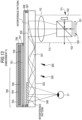
- JP-A-2006-162767 discloses a virtual image display apparatus (image display apparatus) which causes a two-dimensional image formed by an image forming device to be observed by an observer as an enlarged virtual image using a virtual image optical system.
- the image display apparatus 100' includes an image forming device 111 provided with a plurality of pixels arranged in a two-dimensional matrix state, a collimating optical system 112 which converts light emitted from the pixels of the image forming device 111 into parallel light, and an optical device (light guide unit) 120 which guides and emits incident light which has been converted into the parallel light in the collimating optical system 112.
- the optical device 120 includes a light guide plate 121 which causes the incident light to propagate through total reflection and to be emitted, a first deflection unit 130 (for example, formed of a single-layer light reflection film) which reflects the light incident to the light guide plate 121 such that the light incident to the light guide plate 121 is totally reflected inside the light guide plate 121, and a second deflection unit 140 (for example, formed of multi-layer light reflection films having a multi-layer laminate structure) which emits the light which has propagated inside the light guide plate 121 through the total reflection, from the light guide plate 121.
- a first deflection unit 130 for example, formed of a single-layer light reflection film
- a second deflection unit 140 for example, formed of multi-layer light reflection films having a multi-layer laminate structure
- JP-A-2007-94175 discloses a virtual image display apparatus (image display apparatus) which employs a hologram diffraction grating in order to cause a two-dimensional image formed by an image forming device to be observed by an observer as an enlarged virtual image using a virtual image optical system.
- the image display apparatus 300' basically includes an image forming device 111 which displays an image, a collimating optical system 112, and an optical device (light guide unit) 320 to which light displayed in the image forming device 111 is incident and which guides the light to the pupil 21 of the observer.
- the optical device 320 includes a light guide plate 321, and a first diffraction grating member 330 and a second diffraction grating member 340 formed by a reflective volume hologram diffraction grating provided in the light guide plate 321.
- each pixel of the image forming device 111 is incident to the collimating optical system 112, and thus a plurality of parallel light beams of which angles incident to the light guide plate 321 are different are generated by the collimating optical system 112 and are incident to the light guide plate 321.
- the incident parallel light beams are emitted from a first surface 322 of the light guide plate 321.
- the first diffraction grating member 330 and the second diffraction grating member 340 are installed on a second surface 323 of the light guide plate 321, parallel to the first surface 322 of the light guide plate 321.
- an image display apparatus according to Embodiment 3 described with reference to Fig. 13 is referred to in relation to the reference numerals indicating other constituent elements in Fig. 30 .
- image display apparatus 100' or 300' an image is displayed on the image display apparatus 100' or 300', and thereby an observer can observe an external object and the displayed image in an overlapping manner.
- image display apparatuses 100' and 300' are referred to as "semi-transmissive image display apparatuses".
- JP-A-2008-103916 discloses an image display apparatus of a type different from that of the above-described image display apparatuses.
- an observer can observe an image, displayed in the image display apparatus, related to the augmented reality technique but is unable to observe an external object.
- this image display apparatus is referred to as a "non-transmissive image display apparatus".
- WO-A-2006/085310 discloses eyeglass frames with a video camera for capturing an image of the environment.
- the captured image can be displayed by a display source and is then coupled into a light transmitting substrate which is embedded into the frame of the eyeglasses.
- the embodiment can serve in both see-through and non see-through systems.
- a variable filter can be placed in front of the system in such a way that the viewer can control the level of brightness of the light emerging from the external scene.
- the article " Head-mounted displays for medical use” shows the merging of the real world with pre-op or live diagnostic imaging.
- head-mounted displays that merge both real world and registered synthetic imagery are disclosed, so that in addition to the optical see-through views an image captured during the operation or registered before the operation is projected to the user's eyes.
- US-A-2010/0110368 discloses an optical camera that can be positioned in the front of an optic frame for taking images or videos of the user's field of view, and an output device that delivers information to the wearer.
- a display instrument having an image display apparatus which can be used as both of a semi-transmissive image display apparatus and a non-transmissive image display apparatus and enables a composite image in which an image of an external object captured by an imaging apparatus is combined with additional information related thereto with high accuracy through image processing to be favorably viewed via the image display apparatus without being impeded by ambient light, and an image display method using the related display instrument.
- An embodiment of the present disclosure is directed to a display instrument, more specifically a head mounted display (HMD), including (i) a frame that is installed on a head part of an observer; (ii) an image display apparatus that is installed in the frame; and (iii) an imaging apparatus, wherein the image display apparatus includes (A) an image forming device; (B) an optical device that allows light emitted from the image forming device to be incident thereto, to be guided, and to be emitted therefrom; and (C) a dimming device that adjusts a light amount of ambient light incident from the outside, and wherein, in a first mode in which an image captured by the imaging apparatus is displayed on the image display apparatus, the light amount of ambient light incident from the outside is reduced by the dimming device.
- HMD head mounted display
- Another embodiment of the present disclosure is directed to an image display method using a display instrument including (i) a frame that is installed on a head part of an observer; (ii) an image display apparatus that is installed in the frame; and (iii) an imaging apparatus, wherein the image display apparatus includes (A) an image forming device; (B) an optical device that allows light emitted from the image forming device to be incident thereto, to be guided, and to be emitted therefrom; and (C) a dimming device that adjusts a light amount of ambient light incident from the outside, the method including causing the dimming device to reduce the light amount of ambient light incident from the outside in a first mode in which an image captured by the imaging apparatus is displayed on the image display apparatus.
- the dimming device which adjusts a light amount of ambient light incident from the outside, and, in the first mode in which an image captured by the imaging apparatus is displayed on the image display apparatus, the light amount of ambient light incident from the outside is reduced by the dimming device. Therefore, a composite image in which an image of an external object captured by the imaging apparatus is combined with additional information related thereto with high accuracy through an image process can be favorably viewed via the image display apparatus without being impeded by ambient light.
- the device may include an image display apparatus configured to display a captured image of a portion of an environment viewable through the head-mounted display device; and a dimmer configured to, while the captured image is displayed, allow a portion of ambient light from the environment to pass through the dimmer.
- Some embodiments are directed to a method of displaying information on a head-mounted display device.
- the method may include displaying a captured image of a portion of an environment viewable through the display device; and dimming ambient light received through the head-mounted display device from the environment while displaying the captured image.
- the overall image or a portion thereof captured by the imaging apparatus may be displayed in the image forming device in the first mode.
- the image display apparatus functions as a non-transmissive type.
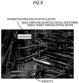
- an image information storage device may be further provided, and, in the first mode, data regarding a subject imaged by the imaging apparatus may be compared with information stored in the image information storage device, and an image of the subject conforming to the information stored in the image information storage device may be displayed on the image display apparatus in a state where a light amount of ambient light incident from the outside is reduced by the dimming device.
- the overall image captured by the imaging apparatus is not displayed on the image display apparatus but an image (or an image which is a portion of the image captured by the imaging apparatus and includes a specific subject) of the specific subject which is a subject conforming to the information stored in the image information storage device is displayed on the image display apparatus.
- the "data regarding a subject imaged by the imaging apparatus” may include, for example, data of extracted feature points of the subject imaged by the imaging apparatus.
- the "information stored in the image information storage device” may include, for example, data of feature points of various objects.
- the "comparison of the data regarding the subject imaged by the imaging apparatus with the information stored in the image information storage device” may include, specifically, for example, a comparison regarding whether extracted feature points of the subject imaged by the imaging apparatus conform to feature points stored in the image information storage device.
- the data regarding the subject imaged by the imaging apparatus may be compared with the information stored in the image information storage device, and information corresponding to the data regarding the subject may be displayed on the image display apparatus. Further, the "information corresponding to the data regarding the subject" will be described later.
- a light amount of ambient light incident to the dimming device is "1"
- a light amount of the ambient light passing through the dimming device is 0.1 or less, and preferably 0.05 or less.
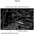
- an image information storage device may be further provided, and, in a second mode different from the first mode, data regarding a subject imaged by the imaging apparatus may be compared with information stored in the image information storage device, and information corresponding to the data regarding the subject may be displayed on the image display apparatus in a state where a light amount of ambient light incident from the outside is not reduced by the dimming device.
- the image display apparatus functions as a semi-transmissive type.
- the "information corresponding to the data regarding the subject" may include, for example, a character, a sentence, a figure, an illustration, a still image, a picture, a moving image, and the like. This is also the same for the following.
- an image information storage device may be further provided, and, in a second mode after an operation in the first mode, data regarding a subject imaged by the imaging apparatus may be compared with information stored in the image information storage device, and information corresponding to the data regarding the subject may be displayed on the image display apparatus in a state where a light amount of ambient light incident from the outside is not reduced by the dimming device.
- the second mode information corresponding to the data regarding the subject may be displayed on the image display apparatus so as to overlap the subject viewed through the dimming device and the optical device or around the subject.
- a microphone may be further provided, and, switching between the first mode and the second mode may be controlled by inputting sound using the microphone. Specifically, switching between the first mode and the second mode may be controlled in response to an instruction based on an observer's voice.
- an infrared-ray emitting and receiving device may be further provided, and switching between the first mode and the second mode may be controlled using the infrared-ray emitting and receiving device.
- the switching between the first mode and the second mode may be controlled by detecting blinking of an observer using the infrared-ray emitting and receiving device.
- a light amount of ambient light incident to the dimming device is "1"
- a light amount of the ambient light passing through the dimming device is 0.3 to 0.8, and preferably 0.5 to 0.8.
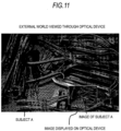
- an image information storage device may be further provided, and, in a third mode different from the first mode (and the second mode), data regarding a subject imaged by the imaging apparatus may be compared with information stored in the image information storage device, and an image (this image is stored in the image information storage device) of the subject having data corresponding to information stored in the image information storage device may be displayed on the image display apparatus in a state where a light amount of ambient light incident from the outside is not reduced by the dimming device.
- the image display apparatus functions as a semi-transmissive type.
- the image display apparatus may further include an image information storage device, and, in the third mode after an operation in the first mode (and/or the second mode), data regarding a subject imaged by the imaging apparatus may be compared with information stored in the image information storage device, and an image (this image is stored in the image information storage device) of the subject having data corresponding to information stored in the image information storage device may be displayed on the image display apparatus in a state where a light amount of ambient light incident from the outside is not reduced by the dimming device.
- a light amount of ambient light incident to the dimming device is "1"
- a light amount of the ambient light passing through the dimming device is 0.1 to 0.6, and preferably 0.3 to 0.4.
- an image of the subject displayed on the image display apparatus may be adjusted so as to overlap the subject viewed through the dimming device and the optical device with the image of the subject displayed on the image display apparatus.
- the adjustment of the image of the subject displayed on the image display apparatus may include enlargement and reduction processes, a rotation process and a movement process of the image, and, specifically, an image data process may be performed based on an affine transform matrix. This is also the same for the following.
- an image of the subject displayed on the image display apparatus may be adjusted such that the image of the subject displayed on the image display apparatus is smaller than the subject viewed through the dimming device and the optical device.
- a pair of image display apparatuses installed in a frame may be provided, and one of the image display apparatuses may be in a state where a light amount of ambient light incident from the outside is not reduced by the dimming device at all times.
- the dimming device may be disposed in the optical device, and, specifically, the dimming device may be disposed on an opposite side (opposite surface) to a side where the image forming device is disposed in the optical device.
- the dimming device may include a light shutter in which a light transmission control material layer is formed of a liquid crystal material layer, or the dimming device may include a light shutter in which the light transmission control material layer is formed of an inorganic electroluminescence material layer.
- the dimming device is not limited thereto, and the dimming device may use a light shutter which includes a plurality of charged electrophoretic particles and an electrophoretic dispersion liquid formed by electrophoretic dispersion media having colors different from those of the electrophoretic particles; a light shutter according to an electrodeposition method employing electrodeposition and dissociation phenomena caused by a reversible oxidation-reduction reaction of a metal (for example, silver particles); a light shutter employing a color variation of a material caused by the oxidation-reduction reaction of an electrochromic material; and a light shutter which controls light transmittance using an electrowetting phenomenon.
- a light shutter which includes a plurality of charged electrophoretic particles and an electrophoretic dispersion liquid formed by electrophoretic dispersion media having colors different from those of the electrophoretic particles
- a light shutter according to an electrodeposition method employing electrodeposition and dissociation phenomena caused by a reversible oxidation-reduction reaction of a metal (for example, silver particles)
- a material constituting the light transmission control material layer may include, for example, a TN (Twisted Nematic) type liquid crystal material, an STN (Super Twisted Nematic) type liquid crystal material, or the like, although not being limited thereto.
- a material constituting the light transmission control material layer may include, for example, tungsten oxide (WO 3 ) although not being limited thereto.
- the optical device and the dimming device are preferably disposed in this order from an observer side; however, the dimming device and the optical device may be disposed in this order.
- a light blocking member which blocks ambient light from being incident to the optical device may be disposed in a region of the optical device to which light emitted from the image forming device is incident.
- this configuration is referred to as a "display instrument related to a first example of the present disclosure".
- the light blocking member which blocks ambient light from being incident to the optical device may be disposed in a region of the optical device to which light emitted from the image forming device is incident.
- the region of the optical device to which light emitted from the image forming device is incident is preferably included in an image in which the light blocking member is projected onto the optical device.
- the light blocking member may be disposed apart from the optical device on an opposite side to the side where the image forming device is disposed in the optical device.
- the light blocking member may be manufactured using, for example, an opaque plastic material.
- This light blocking member may integrally extend from a casing of the image display apparatus or be installed in the casing of the image display apparatus, or may integrally extend from the frame or be installed in the frame.
- the light blocking member may be disposed in the optical device part on an opposite side to the side where the image forming device is disposed, or the light blocking member may be disposed in the dimming device.
- the light blocking member made of an opaque material may be formed on the surface of the optical device using a physical vapor deposition method (a PVD method), a chemical vapor deposition method (a CVD method), or using a printing method, or may be formed by bonding a film, a sheet or a foil made of an opaque material (a plastic material, a metal material, an alloy material, or the like) thereon.
- a projection image of an end portion of the dimming device onto the optical device is preferably included in a projection image of the light blocking member onto the optical device.
- the dimming device may include a first substrate opposite to an optical device; a second substrate opposite to the first substrate; a first electrode and a second electrode respectively provided on the first substrate and the second substrate; and a light transmission control material layer sealed between the first substrate and the second substrate, and the first substrate may also be used as a constituent member of the optical device.
- this configuration is referred to as a "display instrument related to a second example of the present disclosure".
- the first substrate forming the dimming device is also used as a constituent member of the optical device. Thereby, the weight of the entire display instrument can be reduced, and thus there is no concern that a user of the display instrument may feel discomfort.
- the second substrate may be thinner than the first substrate.
- Materials of the first substrate and the second substrate may include, specifically, a transparent glass substrate such as soda-lime glass or super white glass, a plastic substrate, and a plastic sheet, a plastic film.
- the plastic may include polyethylene terephthalate, polyethylene naphtalate, polycarbonate, cellulose esters such as cellulose acetate, fluoropolymers such as a copolymer of polyvinylidene fluoride or polytetrafluoroethylene and hexafluoropropylene, polyethers such as polyoxymethylene, polyolefins such as polyacetal, polystyrene, polyethylene, polypropylene or methylpentene polymer, polyimides such as polyamidoimide or polyetherimide, polyamide, polyethersulfone, polyphenylene sulfide, polyvinylidene fluoride, tetra-acetylcelluose, phenoxy bromide, polyarylate, polysulfone, and the
- the plastic sheet and the plastic film may be rigid so as not to be easily bent, or may be flexible.
- a barrier layer made of an inorganic material or an organic material may be formed on an inner surface of the substrate.
- the first electrode and the second electrode formed on the first substrate and the second substrate may be a so-called transparent electrode, and, specifically, may use indium tin oxide (ITO, including Sn-doped In 2 O 3 , crystalline ITO, and amorphous ITO), fluorine-doped SnO 2 (FTO), IFO (F-doped In 2 O 3 ), antimony-doped SnO 2 (ATO), SnO 2 , ZnO (including Al-doped ZnO or B-doped ZnO), indium zinc oxide (IZO), spinel oxide, oxide with a YbFe 2 O 4 structure, conductive polymers such as polyaniline, polypyrrole or polythiophene, and the like, but are not limited thereto, and may use combinations of two kinds or more thereof.
- ITO indium tin oxide
- FTO fluorine-doped SnO 2
- IFO F-doped In 2 O 3
- ATO antimony-
- the first electrode and the second electrode may be formed using a physical vapor deposition method (PVD method) such as a vacuum deposition method or a sputtering method, various chemical vapor deposition methods (CVD methods), and various coatings.
- PVD method physical vapor deposition method
- CVD methods various chemical vapor deposition methods
- Patterning of the electrode is not basically necessary; however, in a case where patterning is performed as necessary, the patterning may be performed using any method such as an etching method, a lift-off method, or a method using various masks.
- the first substrate and the second substrate are sealed and adhered to each other in the outer edge part by a sealing agent.
- the sealing agent may use a variety of resins, for example, heat-cured type, light-cured type, moisture-cured type, and anaerobic-cured type resins, such as an epoxy resin, a urethane resin, an acryl resin, a vinyl acetate resin, an enethiol resin, a silicone resin, and a degeneration polymer resin.
- a first illuminance sensor (for convenience, referred to as an "environmental illuminance measuring sensor” in some cases) which measures illuminance of the environment in which the display instrument is placed may be further provided, and, based on a measurement result of the first illuminance sensor, light transmittance of the dimming device may be controlled, or luminance of an image formed by the image forming device may be controlled.
- a second illuminance sensor (for convenience, referred to as a "transmission light illuminance measuring sensor” in some cases) which measures illuminance based on light transmitted through the dimming device from the external environment may be further provided, and, based on a measurement result of the second illuminance sensor, light transmittance of the dimming device may be controlled, or luminance of an image formed by the image forming device may be controlled.
- the second illuminance sensor is preferably disposed further toward an observer side than the optical device.
- the transmittance of the dimming device is controlled and the luminance of an image formed by the image forming device is controlled based on a measurement result of the first illuminance sensor
- the transmittance of the dimming device is controlled and the luminance of an image formed by the image forming device is controlled based on a measurement result of the second illuminance sensor
- the illuminance sensors may be formed using existing illuminance sensors, and the illuminance sensors may be controlled using existing control circuits.
- the light transmittance of the dimming device may be made to be equal to or less than a predetermined value (for convenience, referred to as a "first light transmittance” in some cases).
- the light transmittance of the dimming device may be made to be equal to or more than a predetermined value (for convenience, referred to as a "second light transmittance” in some cases).
- the light transmittance of the dimming device may be adjusted while monitoring a value of the second illuminance sensor.
- the first illuminance measurement value may be 10 lux
- the first light transmittance may be any one of 1% to 30%
- the second illuminance measurement value may be 0.01 lux
- the second light transmittance may be any one of 51% to 99%.
- a driving voltage of the dimming device is preferably controlled so as to reduce a driving time, thereby increasing the light transmittance of the dimming device as rapidly as possible.
- light transmitted through the dimming device may be colored in a desired color by the dimming device depending on cases.
- a color of light colored by the dimming device may be variable, or a color of light colored by the dimming device may be fixed.
- a dimming device which colors light red, a dimming device which colors light green, and a dimming device which colors light blue may be laminated.
- a color of light colored by the dimming device may be brown although is not limited thereto.
- the dimming device may be disposed so as to be freely attachable and detachable depending on cases.
- the dimming device may be installed in, for example, the frame using screws made of transparent plastic, the frame may be cut so as to form grooves and the dimming device may be engaged with the grooves, magnets may be installed in the frame and the dimming device may be installed in the frame, or slide portions may be provided in the frame and the dimming device may be fitted and inserted into the slide portions.
- a connector may be installed in the dimming device, and the dimming device may be electrically connected to the control circuit (for example, included in a control device for controlling the image forming device) for controlling the light transmittance of the dimming device via the connector and wires.
- the dimming device may be curved.
- the optical device may include (a) a light guide plate which allows incident light to propagate the inside thereof through total reflection, to be guided, and to be emitted therefrom, (b) a first deflection unit which deflects light incident to the light guide plate such that the light incident to the light guide plate is totally reflected inside the light guide plate, and (c) a second deflection unit which causes the light which has propagated inside the light guide plate through the total reflection to undergo a plurality of deflections in order to emit the light which has propagated inside the light guide plate through the total reflection from the light guide plate.
- total reflection indicates total internal reflection or total reflection inside the light guide plate.
- the second deflection unit may be located in a projection image of the dimming device, or the dimming device may be located in a projection image of the second deflection unit.
- the first deflection unit and the second deflection unit may be covered by one (the first substrate) of the substrates forming the dimming device.
- the optical device is of a semi-transmissive type (see-through type) .
- the optical device part facing the pupil of an observer is semi-transmissive (see-through), thereby allowing viewing of the outside via the optical device part.
- the display instrument may include a single image display apparatus or two image display apparatuses.
- the first deflection unit may reflect light incident to the light guide plate, and the second deflection unit may cause the light which has propagated inside the light guide plate through total reflection to undergo a plurality of transmissions and reflections.
- the first deflection unit may function as a reflective mirror, and the second deflection unit may function as a semi-transmissive mirror.
- the first deflection unit may include, for example, a light reflection film (a kind of mirror) which is made of metal including an alloy and reflects light incident to the light guide plate, or a diffraction grating (for example, a hologram diffraction grating film) which diffracts light incident to the light guide plate.
- the second deflection unit may include a multi-layer laminate structure in which a plurality of dielectric laminate films are laminated, a half mirror, a polarization beam splitter, or a hologram diffraction grating film.
- first deflection unit and the second deflection unit are disposed inside the light guide plate (built in the light guide plate), and, in the first deflection unit, parallel light incident to the light guide plate is reflected or diffracted such that the parallel light incident to the light guide plate is totally reflected inside the light guide plate.
- the parallel light which propagates inside the light guide plate through the total reflection undergoes a plurality of linear reflections or diffractions, and is then emitted from the light guide plate in a parallel light state.
- the first deflection unit may diffract light incident to the light guide plate, and the second deflection unit may cause the light which has propagated inside the light guide plate through the total reflection to undergo a plurality of diffractions.
- the first deflection unit and the second deflection unit may include diffraction grating elements.
- the diffraction grating elements may be formed by a reflective diffraction grating element or a transmissive diffraction grating element, or one of the diffraction grating elements may be formed by a reflective diffraction grating element, and the other thereof may be formed by a transmissive diffraction grating element.
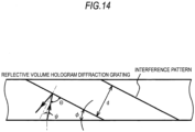
- the reflective diffraction grating element may include a reflective volume hologram diffraction grating.
- first deflection unit formed by the reflective volume hologram diffraction grating is referred to as a "first diffraction grating member”
- second deflection unit formed by the reflective volume hologram diffraction grating is referred to as a "second diffraction grating member”.
- An image may be displayed in a single color (for example, green) by the image display apparatus according to the embodiment of the present disclosure; however, in a case of displaying an image in color, the first diffraction grating member or the second diffraction grating member may be formed by laminating P diffraction grating layers including the reflective volume hologram diffraction grating so as to correspond to diffractive reflection of the P kinds of light beams having the P kinds (for example, P is 3 and the three kinds of red, green and blue) of different wavelength bands (or wavelengths).
- An interference pattern corresponding to one kind of wavelength band (or wavelength) is formed on each diffraction grating layer.
- the P kinds of interference patterns may be formed in the first diffraction grating member or the second diffraction grating member which includes a single diffraction grating layer in order to correspond to diffractive reflection of the P kinds of light beams having the P kinds of different wavelength bands (or wavelengths) .
- an angle of view may be equally divided into, for example, three, and the first diffraction grating member or the second diffraction grating member may be formed by laminating diffraction grating layers corresponding to the respective angles of view.
- first diffraction grating member and the second diffraction grating member including a diffraction grating layer formed by a reflective volume hologram diffraction grating which diffracts and reflects light with a red wavelength band (or wavelength) are disposed in a first light guide plate
- the first diffraction grating member and the second diffraction grating member including a diffraction grating layer formed by a reflective volume hologram diffraction grating which diffracts and reflects light with a green wavelength band (or wavelength) are disposed in a second light guide plate
- the first diffraction grating member and the second diffraction grating member including a diffraction grating layer formed by a reflective volume hologram diffraction grating which diffracts and reflects light with a blue wavelength band (or wavelength) are disposed in a third light guide plate, and the first light guide plate,
- a protection member is preferably disposed such that the reflective volume hologram diffraction grating does not directly contact the air.
- a material of the first diffraction grating member and the second diffraction grating member may be a photopolymer material.
- a constituent material or a basic structure of the first diffraction grating member and the second diffraction grating member including the reflective volume hologram diffraction grating may be the same as a constituent material or a structure of a reflective volume hologram diffraction grating in the related art.
- the reflective volume hologram diffraction grating indicates a hologram diffraction grating which diffracts and reflects only diffraction light of +1 order.
- an interference pattern is formed from the surface to the inside, and a forming method of the related interference pattern itself may be the same as a forming method in the related art.
- a member (for example, a photopolymer material) forming the diffraction grating member may be irradiated with object light from a first predetermined direction on one side, and, simultaneously, the member forming the diffraction grating member may be irradiated with reference light from a second predetermined direction on the other side, such that an interference pattern formed by the object light and the reference light is recorded inside the member forming the diffraction grating member.
- the first predetermined direction, the second predetermined direction, and wavelengths of the object light and the reference light may be appropriately selected, thereby obtaining a desired pitch of the interference pattern and a desired slant angle on the surface of the diffraction grating member.
- the slant angle of the interference pattern indicates an angle formed between a surface of the diffraction grating member (or the diffraction grating layer) and the interference pattern.
- first diffraction grating member and the second diffraction grating member include a laminate structure of P diffraction grating layers formed by the reflective volume hologram diffraction grating
- P diffraction grating layers may be manufactured separately, and the P diffraction grating layers may be laminated (adhered) using, for example, an ultraviolet-cured adhesive.
- diffraction grating layers may be manufactured by sequentially adhering photopolymer materials having the adhesiveness thereon, thereby manufacturing the P diffraction grating layers.
- the optical device may include a semi-transmissive mirror which allows light emitted from the image forming device to be incident thereto and to be emitted therefrom toward the pupil of an observer.
- the light emitted from the image forming device may propagate through the air and be incident to the semi-transmissive mirror, or may propagate inside a transparent member such as, for example, a glass plate or a plastic plate (specifically, a member made of the same material as a material of a light guide plate described later) and be incident to the semi-transmissive mirror.
- the semi-transmissive mirror may be installed in the image forming device via the transparent member, or the semi-transmissive mirror may be installed in the image forming device via a member other than the transparent member.
- the image forming device may include a plurality of pixels arranged in a two-dimensional matrix state.
- this configuration of the image forming device is referred to as an "image forming device with a first configuration".
- the image forming device with the first configuration may include, for example, an image forming device constituted by a reflective spatial light modulation device and a light source; an image forming device constituted by a transmissive spatial light modulation device and a light source; and an image forming device constituted by a light emitting element such as an organic EL (ElectroLuminescence), an inorganic EL, or a light emitting diode (LED), and, among them, the image forming device constituted by a reflective spatial light modulation device and a light source is preferable.
- an image forming device constituted by a reflective spatial light modulation device and a light source may include, for example, an image forming device constituted by a reflective spatial light modulation device and a light source; an image forming device constituted by a transmissive spatial light modulation device and a light source; and an image forming device constituted by a light emitting element such as an organic EL (ElectroLuminescence), an inorganic EL, or a light emitting
- the spatial light modulation device may include a light valve, for example, a transmissive or reflective liquid crystal display such as an LCOS (Liquid Crystal On Silicon) and a digital micromirror device (DMD), and the light source may include a light emitting element.
- the reflective spatial light modulation device may include a liquid crystal display, and a polarization beam splitter which reflects some of light beams from a light source so as to be guided to the liquid crystal display and transmits some of light beams reflected by the liquid crystal display so as to be guided to an optical system.
- the light emitting element forming the light source may include a red light emitting element, a green light emitting element, a blue light emitting element, and a white light emitting element.
- red light, green light, and blue light which are respectively emitted from a red light emitting element, a green light emitting element, and a blue light emitting element may be mixed and undergo luminance uniformity by a light pipe, thereby obtaining white light.
- the light emitting element for example, a semiconductor laser element or a solid-state laser, and an LED may be exemplified.
- the number of pixels may be determined based on specifications required by the image display apparatus, the detailed values of the number of pixels may exemplify 320 ⁇ 240, 432 ⁇ 240, 640 ⁇ 480, 1024 ⁇ 768, 1920 ⁇ 1080, and the like.
- the image forming device may include a light source, and a scanning unit which scans parallel light emitted from the light source.
- the configuration of the image forming device is referred to as an "image forming device with a second configuration".
- a light emitting element is used as the light source, and, specifically, a red light emitting element, a green light emitting element, a blue light emitting element, and a white light emitting element may be used.
- red light, green light, and blue light which are respectively emitted from a red light emitting element, a green light emitting element, and a blue light emitting element may be mixed and undergo luminance uniformity by a light pipe, thereby obtaining white light.
- the light emitting element for example, a semiconductor laser element or a solid-state laser, and an LED may be exemplified.
- the number of pixels (virtual pixels) of the image forming device with the second configuration may also be determined based on specifications required by the image display apparatus, and the detailed values of the number of pixels (virtual pixels) may be exemplified by 320 ⁇ 240, 432 ⁇ 240, 640 ⁇ 480, 1024 ⁇ 768, 1920 ⁇ 1080, and the like.
- the light source is constituted by a red light emitting element, a green light emitting element, and a blue light emitting element
- colors are preferably combined using, for example, a cross prism.
- the scanning unit may use MEMS (Micro Electro Mechanical Systems) or a galvanic mirror which scans light emitted from a light source horizontally and vertically and has, for example, a micromirror capable of rotating in a two-dimensional direction.
- the optical system converts emitted light into parallel light and is referred to as a "parallel light emitting optical system" in some cases, and may be specifically, for example, a collimating optical system or a relay optical system
- this demand for the parallel light is based on it being necessary for light wave surface information when the light is incident to the light guide plate to be preserved even after the light is emitted from the light guide plate via the first deflection unit and the second deflection unit.
- a light emitting portion of the image forming device may be disposed, for example, at a location (position) corresponding to a focal length of the parallel light emitting optical system.
- the parallel light emitting optical system has a function of converting position information of a pixel into angle information in the optical system of the optical device.
- the parallel light emitting optical system may exemplify an optical system which has positive optical power as a whole by using a convex lens, a concave lens, a free-form-surface prism, and a holographic lens, singly or together.
- a light blocking portion having an opening may be disposed between the parallel light emitting optical system and the light guide plate in order to prevent a case where undesired light is emitted from the parallel light emitting optical system and is incident to the light guide plate.
- the light guide plate has two parallel surfaces (a first surface and a second surface) extending in parallel to the axial line (X axis) of the light guide plate.
- the first surface may form the light guide plate incidence surface and the light guide plate emission surface, or the first surface may form the light guide plate incidence surface, and the second surface may form the light guide plate emission surface.
- a material of the light guide plate may use glass including optical glass such as quartz glass or BK7, or a plastic material (for example, PMMA, a polycarbonate resin, an acryl resin, an amorphous polypropylene resin, a styrene resin including an AS resin) .
- a shape of the light guide plate is not limited to a plate shape and may be a curved shape.
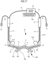
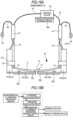
- the frame may include a front portion which is disposed on the front side of an observer, and two temple portions which are installed in both ends of the front portion via hinges so as to be rotatable.
- a modern portion is installed in a front end part of each temple portion.
- the image display apparatus is installed in the frame, specifically, for example, the image forming device may be installed in the temple portions. Further, the front portion and the two temple portions may be integrally formed. In other words, when the overall display instrument according to the embodiment of the present disclosure is viewed, the frame generally has substantially the same structure as glasses.
- a material of the frame including a pad portion may use the same material as a material of typical glasses, such as a metal, an alloy, plastic, and a combination thereof.
- a nose pad may be installed in the front portion.
- an assembly of the frame and the nose pad has substantially the same structure as typical glasses except that there is no rim.
- the nose pad may also have existing configurations and structures.
- wires (a signal line, a power supply line, and the like) of one or two image forming devices preferably extend outward from the front end part of the modern portion via the insides of the temple portion and the modern portion and are connected to the control device (a control circuit or a control unit).
- each image forming device includes a headphone portion, and wires for the headphone portion from each image forming device may extend from the front end part of the modern portion to the headphone portion via the temple portion and the inside of the modern portion.
- the headphone portion may use, for example, an inner ear type headphone portion, or a canal type headphone portion.
- the wire for the headphone portion extends from the front end part of the modern portion to the headphone portion so as to go around the back side of the auricle.
- the imaging apparatus may be installed at the central part of the front portion.
- the imaging apparatus includes, specifically, a solid-state imaging element formed by, for example, a CCD or a CMOS sensor, and a lens. Wires from the imaging apparatus may be connected to one of the image display apparatuses (or the image forming devices) via, for example, the front portion, and, further, may be included in wires extending from the image display apparatus (or the image forming device).
- central light beams Light beams which are emitted from the center of the image forming device and pass through a node on the image forming device side of the optical system are referred to as "central light beams", and, among the central light beams, a central light beam which is perpendicularly incident to the optical device is referred to as a "central incident light beam".
- a point where the central incident light beam is incident to the optical device is set as a central point of the optical device
- an axial line which passes through the central point of the optical device and is parallel to the axial line direction of the optical device is set as an X axis
- an axial line which passes through the central point of the optical device and conforms to the normal line of the optical device is set as a Y axis.
- a horizontal direction in the display instrument or the like according to the embodiment of the present disclosure is a direction parallel to the X axis, and is hereinafter referred to as an "X axis direction" in some cases.
- the optical system is disposed between the image forming device and the optical device and converts light emitted from the image forming device into parallel light.
- a light flux converted into the parallel light in the optical system is incident to the optical device, is guided and is emitted therefrom.
- a central point of the first deflection unit is set as an "optical device central point".
- the display instrument or the like including the above-described various modified examples may be used for display of, for example, various descriptions, or symbols, signs, marks, labels, designs, and the like when observation targets (subjects) such as various devices are worked, operated, maintained, and dismantled; display of various descriptions, or symbols, signs, marks, labels, designs, and the like regarding observation targets (subjects) such as persons or products; display of moving images or still images; display of subtitles of a movie or the like; display of an explanation or a closed caption regarding a picture synchronized with the picture; display of various descriptions regarding observation targets (subjects) in a play or a kabuki play, a noh play, a comedic drama, an opera, a concert, a ballet, various theaters, an amusement park, an art gallery, a tourist spot, a resort area, travel guidance, and the like, and an explanation for explaining content, progress, background thereof, or the like, or display of closed captions.
- observation targets such as various devices are worked, operated,
- the above-described variety of content represents information corresponding to data regarding a subject.
- a play or a kabuki play a noh play, a comedic drama, an opera, a concert, a ballet, various theaters, an amusement park, an art gallery, a tourist spot, a resort area, travel guidance, and the like
- characters related to an observation target may be displayed as an image on the display instrument at an appropriate timing.
- an image control signal is sent to the display instrument, and an image is displayed on the display instrument, by an operator's operation or under the control of a computer or the like, based on a predetermined schedule and allocation of time.
- observation targets such as various devices, persons or products
- observation targets such as various devices, persons or products
- the display instrument or the like according to the embodiment of the present disclosure may be used as a stereoscopic display instrument.
- a polarization plate or a polarization film may be installed in the optical device so as to be attachable and detachable, or a polarization plate or a polarization film may be bonded to the optical device, depending on cases.
- Image signals applied to the image forming device may include not only an image signal (for example, character data) but also, for example, luminance data (luminance information) regarding an image to be displayed, or chromaticity data (chromaticity information), or luminance data and chromaticity data.
- the luminance data may be luminance data corresponding to the luminance of a predetermined region including an observation target viewed through the optical device
- the chromaticity data may be chromaticity data corresponding to the chromaticity of a predetermined region including an observation target viewed through the optical device.
- the luminance data regarding an image is included, thereby controlling the luminance (brightness) of the displayed image
- the chromaticity data regarding an image is included, thereby controlling the chromaticity (color) of the displayed image
- the luminance data and the chromaticity data regarding an image are included, thereby controlling the luminance (brightness) and the chromaticity (color) of the displayed image.
- a value of the luminance data may be set such that the higher the value of the luminance of the predetermined region including the observation target viewed through the image display apparatus, the higher the value of the luminance of the image (that is, the more brightly the image is displayed).
- a value of the chromaticity data may be set such that the chromaticity of the predetermined region including the observation target viewed through the image display apparatus and the chromaticity of an image to be displayed have a substantially complementary color relationship.
- the complementary color indicates a combination of colors located directly opposite to each other in the color circle.
- Examples of the complementary colors include red and green, yellow and violet, blue and orange, and the like.
- a color causing chroma reduction is also specified like white in a case of light and black in a case of an object when a certain color is mixed with other colors at an appropriate ratio
- the visual effect complementation when colors are arranged in parallel is different from the visual effect complementation when the colors are mixed.
- the colors are also called complemental colors, contrasting colors, or opposite colors.
- the opposite colors directly indicate opposite colors, whereas a range indicated by the complementary colors is a slightly wider.
- a combination of complementary colors causes the synergistic effect of uniting the colors so as to support each other, which is called complementary color harmony.
- Embodiment 1 relates to a display instrument and an image display method according to embodiment of the present disclosure.
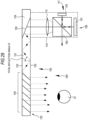
- Fig. 1 is a conceptual diagram illustrating an image display apparatus according to Embodiment 1;
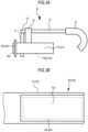
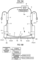
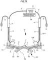
- Fig. 2 is a schematic diagram of the display instrument (specifically, a head mounted display (HMD)) of Embodiment 1 and the like, viewed from the top side;
- Fig. 3A is a schematic diagram of the display instrument viewed from the lateral side;
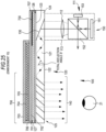
- Fig. 3B is a schematic diagram of optical device and dimming device parts viewed from the front side;
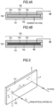
- Figs. 4A and 4B are schematic cross-sectional views of the dimming device schematically illustrating a behavior of the dimming device in the display instrument of Embodiment 1.
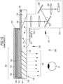
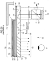
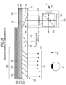
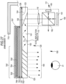
- Fig. 5 is a diagram schematically illustrating propagation of light in a light guide plate forming the image display apparatus.
- the display instrument of Embodiment 1 or Embodiments 2 to 12 described later is more specifically a head mounted display (HMD), and includes (i) a frame (for example, a glasses-type frame 10) worn on the head part of an observer, (ii) an image display apparatus 100, 200, 300, 400 or 500 installed in the frame 10, and (iii) an imaging apparatus 17.
- a frame for example, a glasses-type frame 10
- an imaging apparatus 17 an imaging apparatus 17
- the display instrument of Embodiment 1 or Embodiments 2 to 12 described later is, specifically, of a binocular type in which two image display apparatuses are provided
- the display instrument may be of a monocular type in which a single image display apparatus is provided.
- the image forming device 111 or 211 displays, for example, a monochrome (for example, green) image.
- the image display apparatus 100, 200, 300, 400 or 500 in Embodiment 1 or Embodiments 2 to 12 described later includes (A) the image forming device 111 or 211, (B) an optical device (a light guide unit) 120, 320 or 520 which allows light emitted from the image forming device 111 or 211 to be incident thereto, to be guided, and to be emitted therefrom, (C) a dimming device 700 which adjusts a light amount of ambient light incident from the outside, and (D) an optical system (parallel light emitting optical system) 112 or 254 which converts light emitted from the image forming device 111 or 211 into parallel light.
- a light flux which has been converted into parallel light in the optical system 112 or 254 is incident to, is guided, and is emitted from the optical device 120, 320 or 520.
- the image display apparatus 100, 200, 300, 400 or 500 may be installed in the frame so as to be fixed, or may be installed so as to be attachable and detachable.
- the optical system 112 or 254 is disposed between the image forming device 111 or 211 and the optical device 120, 320 or 520.
- a light flux which is converted into parallel light in the optical system 112 or 254 is incident to, is guided, and is emitted from the optical device 120, 320 or 520.
- the optical device 120, 320 or 520 is of a semi-transmissive type (a see-through type).
- at least optical device parts (more specifically, light guide plates 121 or 321 and second deflection units 140 or 340 described later) facing both eyes of the observer are semi-transmissive (see-through).
- Embodiment 1 or Embodiments 2 to 7 described later among light beams (central light beams CL) which are emitted from the center of the image forming device 111 or 211 and pass through a node on the image forming device side of the optical system 112 or 254, a point where a central incident light beam which is perpendicularly incident to the optical device 120 or 320 is incident to the optical device 120, 320 or 520 is set as an optical device central point O.
- an axial line which passes through the optical device central point O and is parallel to the axial line direction of the optical device 120, 320 or 520 is set as an X axis
- an axial line which passes through the optical device central point O and conforms to the normal line of the optical device 120, 320 or 520 is set as a Y axis.
- a central point of the first deflection unit 130 or 330 described below is the optical device central point O. That is to say, as shown in Fig.
- the central incident light beam CL which is emitted from the center of the image forming device 111 or 211 and passes through the node on the image forming device side of the optical system 112 or 254 vertically runs into the light guide plate 121 or 321.
- the central incident light beam CL is incident to the light guide plate 121 or 321 at an incidence angle of 0°.
- a center of a displayed image conforms to the perpendicular line direction of the first surface 122 or 322 of the light guide plate 121 or 321.
- the dimming device 700 which adjusts a light amount of ambient light incident from the outside is disposed on an opposite side to the side where the image forming device 111 or 211 of the optical device 120, 320 or 520 is disposed.
- the dimming device 700 which is a kind of light shutter is fixed to the optical device 120, 320 or 520 (specifically, a protection member (protection plate) 126 or 326 for protecting the light guide plate 121 or 321 or a semi-transmissive mirror 520) using an adhesive 707.
- the dimming device 700 is disposed in a region of the optical device 120, 320 or 520 on an opposite side to the observer.
- the protection member (a protection plate) 126 or 326 is adhered to the second surface 123 or 323 of the light guide plate 121 or 321 by an adhesive member 127 or 327, and the first deflection unit 130 or 330 and the second deflection unit 140 or 340 are covered by the protection member (a protection plate) 126 or 326.
- the optical device 120 or 320 in the Embodiment 1 or Embodiments 2 to 4 and Embodiments 6 to 12 described later includes (a) the light guide plate 121 or 321 that causes incident light to propagate to an inside thereof through total reflection and to be emitted therefrom, (b) the first deflection unit 130 or 330 that deflects the light incident to the light guide plate 121 or 321 such that the light incident to the light guide plate 121 or 321 is totally reflected inside the light guide plate 121 or 321, and (c) the second deflection unit 140 or 340 that causes the light which has propagated inside the light guide plate 121 or 321 through the total reflection to undergo a plurality of deflections such that the light which has propagated inside the light guide plate 121 or 321 through the total reflection is emitted from the light guide plate 121 or 321.
- the second deflection unit 140 or 340 is located in a projection image of the dimming device 700.
- the first deflection unit 130 and the second deflection unit 140 are disposed inside the light guide plate 121.
- the first deflection unit 130 reflects light incident to the light guide plate 121
- the second deflection unit 140 causes the light which has propagated inside the light guide plate 121 through the total reflection to undergo a plurality of transmissions and reflections.
- the first deflection unit 130 functions as a reflective mirror
- the second deflection unit 140 functions as a semi-transmissive mirror.
- the first deflection unit 130 disposed inside the light guide plate 121 is made of aluminum (Al), and includes a light reflection film (a kind of mirror) which reflects light incident to the light guide plate 121.
- the second deflection unit 140 provided inside the light guide plate 121 includes a multi-layer laminate structure in which a plurality of dielectric laminate films are laminated.
- the dielectric laminate film includes, for example, a TiO 2 film which is a high dielectric constant material, and a SiO 2 film which is a low dielectric constant material.
- the multi-layer laminate structure in which a plurality of dielectric laminate films are laminated is disclosed in JP-T-2005-521099 . Although six-layer dielectric laminate films are shown in the figures, the present disclosure is not limited thereto.
- a thin piece made of the same material as a material of the light guide plate 121 is interposed between the dielectric laminate film and the dielectric laminate film.
- the parallel light incident to the light guide plate 121 is reflected (or diffracted) such that the parallel light incident to the light guide plate 121 is totally reflected inside the light guide plate 121.
- the parallel light which has propagated inside the light guide plate 121 through the total reflection undergoes a plurality of reflections (diffractions) and is emitted from the light guide plate 121 toward the pupil 21 of the observer in a parallel light state.
- a part 124 in which the first deflection unit 130 of the light guide plate 121 is provided may be cut so as to provide a tilt surface on which the first deflection unit 130 is formed in the light guide plate 121, and the cut part 124 of the light guide plate 121 may be adhered to the first deflection unit 130 after a light reflection film is vacuum-deposited on the related tilt surface.
- a multi-layer laminate structure in which the same material (for example, glass) as a material of the light guide plate 121 and a plurality of dielectric laminate films (can be formed in a vacuum deposition method, for example) are laminated may be manufactured, a part 125 on which the second deflection unit 140 is provided in the light guide plate 121 may be cut so as to form a tilt surface, and the multi-layer laminate structure may be adhered to the related tilt surface and be polished so as to trim the exterior.
- the optical device 120 in which the first deflection unit 130 and the second deflection unit 140 are provided inside the light guide plate 121.
- the light guide plate 121 or 321 made of optical glass or a plastic material has two parallel surfaces (the first surface 122 or 322 and the second surface 123 or 323) which extend in parallel to the light propagation direction (X axis) through the total internal reflection of the light guide plate 121 or 321.
- the first surface 122 or 322 faces the second surface 123 or 323.
- parallel light is incident from the first surface 122 or 322 corresponding to a light incidence surface, then propagates inside the light guide plate through total reflection, and is emitted from the first surface 122 or 322 corresponding to a light emission surface.
- the present disclosure is not limited thereto, and the light incidence surface may be formed by the second surface 123 or 323, and the light emission surface may be formed by the first surface 122 or 322.
- the image forming device 111 is an image forming device with a first configuration, and has a plurality of pixels arranged in a two-dimensional matrix state.
- the image forming device 111 includes a reflective spatial light modulation device 150, and a light source 153 constituted by a light emitting diode emitting white light.
- Each image forming device 111 is entirely accommodated in a casing 113 (indicated by the dot chain line in Fig. 1 ), an opening (not shown) is provided in the related casing 113, and light is emitted from the optical system (a parallel light emitting optical system or a collimating optical system) 112 via the opening.
- the reflective spatial light modulation device 150 includes a liquid crystal display (LCD) 151 formed from an LCOS which is a light value, and a polarization beam splitter 152 which reflects some of light from the light source 153 so as to be guided to the liquid crystal display 151 and transmits some of light reflected by the liquid crystal display 151 therethrough so as to be guided to the optical system 112.
- the liquid crystal display 151 includes a plurality (for example, 640 ⁇ 480) of pixels (liquid crystal cells) arranged in a two-dimensional matrix state.
- the polarization beam splitter 152 has an existing configuration and structure. Non-polarized light emitted from the light source 153 runs into the polarization beam splitter 152.
- a P polarization component passes through the polarization beam splitter 152 and is emitted outward.
- an S polarization component is reflected by the polarization beam splitter 152 so as to be incident to the liquid crystal display 151, is reflected inside the liquid crystal display 151, and is emitted from the liquid crystal display 151.
- the light beams emitted from the liquid crystal display 151 the light beams emitted from the pixels displaying "white” include many P polarization components, and the light beams emitted from the pixels displaying "black” include many S polarization components.
- the optical system 112 includes, for example, a convex lens and generates parallel light, and thus the image forming device 111 (more specifically, the liquid crystal display 151) is disposed at a location (position) corresponding to the focal length in the optical system 112.
- the frame 10 includes a front portion 11 which is disposed on the front side of the observer, two temple portions 13 which are installed at both ends of the front portion 11 via hinges 12 so as to rotatably move, and a modern portion (also called a tip cell, an earmuff, or an ear pad) 14 which is installed in a front end part of each of the temple portions 13.
- a nose pad (not shown) is installed.
- an assembly of the frame 10 and the nose pad basically has substantially the same structure as typical glasses.
- the respective casings 113 are installed in the temple portions 13 so as to be attachable and detachable using installation members 19.
- the frame 10 is manufactured using metal or plastic.
- the respective casings 113 may be installed in the temple portions 13 so as not to be attachable and detachable using the installation members 19. Further, in an observer who possesses and wears the glasses, the respective casings 113 may be installed in the temple portions of the frame of the glasses of the observer so as to be attachable and detachable using the installation members 19. The respective casings 113 may be installed outside the temple portions 13 or may be installed inside the temple portions 13.
- wires (a signal line, a power supply line, and the like) 15 extending from one of the image forming devices 111A extend outward from the front end part of the modern portion 14 via the temple portion 13 and the inside of the modern portion 14 and are connected to a control device (a control circuit, or a control unit) 18.
- each of the image forming devices 111A and 111B includes a headphone portion 16, and a wire 16' for the headphone portion extending from each of the image forming devices 111A and 111B extends from the front end part of the modern portion 14 to the headphone portion 16 via the temple portion 13 and the inside of the modern portion 14.
- the wire 16' for the headphone portion extends from the front end part of the modern portion 14 to the headphone portion 16 so as to go around the back side of the auricle.
- the wires (a signal line, a power supply line, and the like) 15 are connected to the control device (control circuit) 18 as described above.
- the control device 18 includes an image information storage device 18A.
- processes for displaying images are performed in the control device 18.
- the control device 18 and the image information storage device 18A may be formed using existing circuits.
- the imaging apparatus 17 including a solid-state imaging element formed using a CCD or a CMOS sensor and a lens (not shown) is installed in a central part 11' of the front portion 11 via an appropriate installation member (not shown).
- a signal from the imaging apparatus 17 is sent to, for example, the image forming device 111A via a wire (not shown) extending from the imaging apparatus 17.
- the dimming device 700 in Embodiment 1 includes a light shutter in which a light transmission control material layer 705 is formed of a liquid crystal material layer.
- the dimming device 700 includes a transparent first substrate 701 opposite to the optical device 120, a transparent second substrate 703 opposite to the first substrate 701, electrodes 702 and 704 respectively provided on the first substrate 701 and the second substrate 703, and the light transmission control material layer 705 sealed between the first substrate 701 and the second substrate 703.
- the first substrate 701 and the second substrate 703 are made of a plastic material.
- the first electrode 702 and the second electrode 704 include transparent electrodes made of indium tin oxide (ITO), and are formed using a combination of a PVD method such as a sputtering method and a lift-off method.
- the light transmission control material layer 705 is formed of, specifically, a liquid crystal material layer using a TN (Twisted Nematic) type liquid crystal material.
- the first electrode 702 and the second electrode 704 are so-called beta electrodes which are not patterned.
- the first electrode 702 and the second electrode 704 are connected to the control device 18 via a connector and a wire (neither shown). Outer edge parts of the two substrates 701 and 703 are sealed by a sealing agent 706.
- the first substrate 701 of the dimming device 700 is adhered to a protection member 126 (protecting the light guide plate 121) by an adhesive 707.
- polarization films are respectively bonded to the outer surface of the first substrate 701 and the outer surface of the second substrate 703, and these polarization films are not shown.
- the first substrate 701 of the dimming device 700 is made to be shorter than the light guide plate 121, and the first substrate 701 of the dimming device 700 is fixed to the protection member 126 by the adhesive 707.
- the adhesive 707 is disposed at the outer edge part of the first substrate 701. This is also the same for the embodiments described in the following.
- the optical device 120 and the dimming device 700 are disposed in this order from the observer.
- the light transmittance of the dimming device 700 can be controlled by voltages applied to the first electrode 702 and the second electrode 704. Specifically, for example, when a voltage is applied to the first electrode 702 in a state where the second electrode 704 is grounded, an arrangement state of liquid crystals in the liquid crystal material layer forming the light transmission control material layer 705 varies, and thereby the light transmittance of the liquid crystal material layer varies (refer to Figs. 4A and 4B ). Voltages applied to the first electrode 702 and the second electrode 704 can be controlled by the observer operating a control knob provided in the control device 18. In other words, the light transmittance of the dimming device 700 may be adjusted while the observer observes an image from the optical device 120 or 320.
- a light amount of ambient light incident from the outside is reduced by the dimming device 700 in a first mode in which an image captured by the imaging apparatus 17 is displayed on the image display apparatus 100, 200, 300, 400 or 500.
- the image display apparatus 100, 200, 300, 400 or 500 functions as a non-transmissive type.
- Fig. 6 shows the external world viewed through the optical device (a light guide unit) 120, 320 or 520.
- a "subject A" imaged by the imaging apparatus 17 is set to a screwdriver placed under the tools.
- the grip part and the front end part of the screwdriver are set as feature points of the screwdriver which is the subject A.
- the overall image captured by the imaging apparatus 17 is displayed in the image forming devices 111A and 111B.
- an image (an image viewed in the optical device 120, 320 or 520 by the observer) displayed on the image display apparatus 100, 200, 300, 400 or 500 is shown in Fig. 7A .
- data regarding a subject (specifically, the subject A in this case) imaged by the imaging apparatus 17 may be compared with information stored in the image information storage device 18A, and information (specifically, character information such as a "screwdriver") corresponding to the data regarding the subject (the subject A) conforming to the information stored in the image information storage device 18A may be displayed around the subject A as shown in Fig. 7A , or be displayed so as to overlap the subject A. Alternatively, only the image captured by the imaging apparatus 17 may be displayed without displaying this information.
- the data regarding the subject imaged by the imaging apparatus may be, for example, data of extracted feature points of the subject imaged by the imaging apparatus 17.
- the information stored in the image information storage device may be, for example, data of feature points of various objects. Further, specifically, for example, a comparison may be performed with regard to whether extracted feature points of the subject imaged by the imaging apparatus conform to feature points stored in the image information storage device.
- data regarding a subject imaged by the imaging apparatus 17 may be compared with information stored in the image information storage device 18A, and an image of the subject (the subject A in this example) conforming to the information stored in the image information storage device 18A may be displayed on the image display apparatus 100, 200, 300, 400 or 500 in a state where a light amount of ambient light incident from the outside is reduced by the dimming device 700 (that is, in a state where the first mode is continued) (refer to Fig. 7B ) .
- an enhancement process for example, a color being added to the outline of the subject A
- data regarding the subject imaged by the imaging apparatus 17 may be compared with the information stored in the image information storage device 18A, and information (specifically, for example, character data such as a "screwdriver") corresponding to the data regarding the subject may be displayed on the image display apparatus 100, 200, 300, 400 or 500 in a state where a light amount of ambient light incident from the outside is reduced by the dimming device 700, that is, an image of the external environment is viewed in the optical device (a light guide unit) 120, 320 or 520 (that is, in a state where the first mode is continued) .
- information specifically, for example, character data such as a "screwdriver”
- the information corresponding to the data regarding the subject is displayed so as to overlap the image of the subject in the image displayed on the optical device 120, 320 or 520 or around the image of the subject (refer to Fig. 8 ), and this will be described later in detail.
- a light amount of the ambient light passing through the dimming device is 0.1 or less, and preferably 0.05 or less.
- an operation mode of the image display apparatus 100, 200, 300, 400 or 500 is switched from the first mode to a second mode.
- the mode switching between the first mode and the second mode may be performed by inputting sound using a provided microphone (not shown) (an instruction based on an observer's voice).
- the mode switching may be performed using a provided infrared-ray emitting and receiving device (not shown), and, specifically, may be performed by detecting blinking of the observer using the infrared-ray emitting and receiving device.
- the image display apparatus 100, 200, 300, 400 or 500 functions as a semi-transmissive type, and, data regarding the subject imaged by the imaging apparatus 17 may be compared with the information stored in the image information storage device 18A, and information (specifically, for example, character data such as a "screwdriver") corresponding to the data regarding the subject may be displayed on the image display apparatus in a state where a light amount of ambient light incident from the outside is not reduced by the dimming device 700, that is, the external world are viewed through the optical device (a light guide unit) 120, 320 or 520.
- information specifically, for example, character data such as a "screwdriver”
- the information corresponding to the data regarding the subject is displayed so as to overlap the subject viewed from the dimming device 700 and optical device 120, 320 or 520 or around the subject (refer to Fig. 8 ), and this will be described later in detail.
- a light amount of the ambient light passing through the dimming device 700 is 0.3 to 0.8, and preferably 0.5 to 0.8.
- the operation mode of the image display apparatus 100, 200, 300, 400 or 500 is switched from the first to a third mode.
- the mode switching between the first mode and the third mode may be performed in the same method as the mode switching between the first mode and the second mode.
- data regarding the subject imaged by the imaging apparatus 17 may be compared with the information stored in the image information storage device 18A, and an image (specifically, an image of the subject A) of the subject having data corresponding to information stored in the image information storage device 18A may be displayed on the image display apparatus 100, 200, 300, 400 or 500 in a state where a light amount of ambient light incident from the outside is not reduced by the dimming device 700, that is, the image display apparatus functions as a semi-transmissive type and the external world are viewed through the optical device (light guide unit) 120, 320 or 520.
- the image of the subject A is displayed so as to overlap the subject A viewed through the dimming device 700 and the optical device 120, 320 or 520.
- a light amount of the ambient light passing through the dimming device 700 is 0.1 to 0.6, and preferably 0.3 to 0.4.
- the subject viewed through the dimming device 700 and the optical device 120, 320 or 520 overlaps the image of the subject displayed on the image display apparatus 100, 200, 300, 400 or 500 by adjusting the image of the subject displayed on the image display apparatus 100, 200, 300, 400 or 500.
- the image of the subject displayed on the image display apparatus 100, 200, 300, 400 or 500 may undergo enlargement and reduction processes, a rotation process, and a movement process while viewing the subject through the dimming device 700 and the optical device 120, 320 or 520.
- an image data process may be performed based on an affine transform matrix.
- the image displayed on the optical device 120, 320 or 520 is moved horizontally and vertically, is rotatably moved, or is enlarged and reduced using a switch (not shown) disposed in the control device 18. Thereby, a display position correcting signal is generated in the control device 18, and an image signal is superimposed on the display position correcting signal.
- the image display apparatus 100, 200, 300, 400 or 500 displays the information corresponding to the data regarding the subject so as to overlap the image of the subject in the image displayed on the optical device 120, 320 or 520 or around the image of the subject
- the image display apparatus 100, 200, 300, 400 or 500 displays the information corresponding to the data regarding the subject so as to overlap the subject viewed through the dimming device 700 and the optical device 120, 320 or 520 or around the subject; however, the above-described processes may be performed before this display.
- overlapping with the subject A may be performed, or, as shown in Fig. 10 , an image which is a portion of the image captured by the imaging apparatus 17 and includes a specific subject (the subject A) may be displayed on the image display apparatus 100, 200, 300, 400 or 500.
- a portion of the image captured by the imaging apparatus 17 is indicated by the white range.
- the image of the subject displayed on the image display apparatus 100, 200, 300, 400 or 500 is adjusted such that the image of the subject displayed on the image display apparatus is smaller than the subject viewed through the dimming device 700 and the optical device 120, 320 or 520 (refer to Fig. 11 ).
- the reduced image is indicated by the white range.
- one image display apparatus for example, a right eye image display apparatus
- the other image display apparatus for example, a left eye image display apparatus
- the dimming device 700 may perform the above-described operations
- the other image display apparatus for example, a left eye image display apparatus
- the dimming device which adjusts a light amount of ambient light incident from the outside is disposed in the optical device, and, in the first mode in which an image captured by the imaging apparatus is displayed on the image display apparatus, a light amount of ambient light incident from the outside is reduced by the dimming device.
- the display instrument can be used as both the non-transmissive image display apparatus and the semi-transmissive image display apparatus on the basis of control of operations and non-operations of the dimming device.
- a light amount of ambient light incident from the outside is reduced by the dimming device, it is possible to match an external object with a displayed image with high accuracy.
- Embodiment 2 is a modification of Embodiment 1.
- the image forming device 211 includes an image forming device with the second configuration in Embodiment 2.
- a light source 251 and a scanning unit 253 which scans parallel light emitted from the light source 251 are provided.
- the image forming device 211 includes (i) the light source 251, (ii) a collimating optical system 252 which converts light emitted from the light source 251 into parallel light, (iii) the scanning unit 253 which scans the parallel light emitted from the collimating optical system 252, and (iv) a relay optical system 254 which relays the parallel light scanned by the scanning unit 253 so as to be emitted.
- each image forming device 211 is entirely accommodated in a casing 213 (indicated by the dot chain line in Fig. 12 ), an opening (not shown) is provided in the related casing 213, and light is emitted from the relay optical system 254 via the opening.
- the respective casings 213 are installed in the temple portions 13 so as to be attachable and detachable using installation members 19.
- the light source 251 includes a light emitting element which emits white light.
- light emitted from the light source 251 is incident to the collimating optical system 252 which has positive optical power as a whole and is emitted as parallel light.
- the parallel light is reflected by a total reflection mirror 256, and undergoes horizontal scanning and vertical scanning by the scanning unit 253 including MEMS which can scan incident parallel light in a two-dimensional manner by using a micromirror which freely rotates in a two-dimensional direction, thereby generating a kind of two-dimensional image and virtual pixels (the number of pixels may be the same as in Embodiment 1).
- the light from the virtual pixels passes through the relay optical system (a parallel light emitting optical system) 254 formed of an existing relay optical system, and a light flux converted into parallel light is incident to the optical device 120.
- the optical device 120 which causes the light flux converted into parallel light in the relay optical system 254 to be incident thereto, be guided and be emitted therefrom has the same configuration and structure as the optical device described in Embodiment 1, and thus detailed description thereof will be omitted.
- the display instrument of Embodiment 2 has substantially the same configuration and structure as the display instrument of Embodiment 1 except for the image forming device 211 is different, and thus detailed description thereof will be omitted.
- Embodiment 3 is also a modification of Embodiment 1.
- Fig. 13 is a conceptual diagram of the image display apparatus 300 in the display instrument (head mounted display) of Embodiment 3.
- Fig. 14 is a schematic cross-sectional view illustrating an enlarged portion of a reflective volume hologram diffraction grating.
- the image forming device 111 includes an image forming device with the first configuration in the same manner as in Embodiment 1.
- basic configuration and structure of the optical device 320 are the same as the optical device 120 of Embodiment 1 except that configuration and structures of the first deflection unit and the second deflection unit are different.
- the first deflection unit and the second deflection unit are disposed on a surface of the light guide plate 321 (specifically, the second surface 323 of the light guide plate 321).
- the first deflection unit diffracts light incident to the light guide plate 321
- the second deflection unit causes the light which has propagated inside the light guide plate 321 through total reflection to undergo a plurality of diffractions.
- the first deflection unit and the second deflection unit includes a diffraction grating element, specifically, a reflective diffraction grating element, more specifically, a reflective volume hologram diffraction grating.
- the first deflection unit including the reflective volume hologram diffraction grating is referred to as a "first diffraction grating member 330"
- the second deflection unit formed by the reflective volume hologram diffraction grating is referred to as a "second diffraction grating member 340".
- the first diffraction grating member 330 and the second diffraction grating member 340 are formed by laminating a single diffraction grating layer.
- an interference pattern corresponding to one kind of wavelength band (or a wavelength) is formed on each diffraction grating layer made of a photopolymer material and is manufactured in a method in the related art.
- a pitch of the interference pattern formed on the diffraction grating layer (diffraction optical element) is constant, and the interference pattern is linear and is parallel to the Z axis.
- the axial lines of the first diffraction grating member 330 and the second diffraction grating member 340 are parallel to the X axis, and the normal lines thereof are parallel to the Y axis.
- Fig. 14 is a partial cross-sectional view illustrating an enlarged reflective volume hologram diffraction grating.
- An interference pattern with a slant angle ⁇ is formed in the reflective volume hologram diffraction grating.
- the slant angle ⁇ indicates an angle formed between the surface of the reflective volume hologram diffraction grating and the interference pattern.
- the interference pattern is formed from the inside of the reflective volume hologram diffraction grating to the surface.
- the interference pattern satisfies the Bragg condition.
- the Bragg condition indicates a condition satisfying the following Equation (A).
- Equation (A) m indicates a positive integer, ⁇ indicates a wavelength, d indicates a pitch of the grating surface (an interval in the normal direction of a virtual plane including the interference pattern), and ⁇ indicates the complementary angle of an incidence angle to the interference pattern.
- the first diffraction grating member 330 is disposed on (adhered to) the second surface 323 of the light guide plate 321, and diffracts and reflects parallel light incident to the light guide plate 321 such that the parallel light incident to the light guide plate 321 from the first surface 322 is totally reflected inside the light guide plate 321.
- the second diffraction grating member 340 is disposed on (adhered to) the second surface 323 of the light guide plate 321, and causes the parallel light which has propagated inside the light guide plate 321 through the total reflection to undergo a plurality of diffractions and reflections and to be emitted from the first surface 322 in a parallel light state from the light guide plate 321.
- the parallel light propagates inside the light guide plate 321 through the total reflection and is then emitted.
- the number of total reflections until reaching the second diffraction grating member 340 is different depending on each angle of view. More specifically, of the parallel light beams incident to the light guide plate 321, the number of reflections of a parallel light beam incident with an angle in a direction close to the second diffraction grating member 340 is smaller than the number of reflections of a parallel light beam incident to the light guide plate 321 with an angle in a direction distant from the second diffraction grating member 340.
- the parallel light which is diffracted and reflected in the first diffraction grating member 330 and is incident to the light guide plate 321 at an angle in a direction close to the second diffraction grating member 340 has a smaller angle formed with the normal line of the light guide plate 321 when the light propagating inside the light guide plate 321 runs into the inner surface of the light guide plate 321 than the parallel light incident to the light guide plate 321 at an angle in a reverse direction thereto.
- a shape of the interference pattern formed inside the second diffraction grating member 340 and a shape of the interference pattern formed inside the first diffraction grating member 330 are symmetric with respect to a virtual plane perpendicular to the axial line of the light guide plate 321.
- the surfaces of the first diffraction grating member 330 and the second diffraction grating member 340 which do not face the light guide plate 321 are covered by a protection member (a protection plate) 326 such that the first diffraction grating member 330 and the second diffraction grating member 340 are prevented from being damaged.
- the light guide plate 321 and the protection member 326 are adhered to each other by an adhesive 327 at the outer circumferential part.
- the light guide plate 321 may be protected by bonding a transparent protection film to the first surface 322.
- the light guide plate 321 in Embodiment 4 described later basically also has the same configuration and structure as the above-described configuration and structure of the light guide plate 321.
- the display instrument of Embodiment 3 has substantially the same configuration and structure as the display instrument of Embodiment 1 except that the optical device 320 is different as described above, and thus detailed description thereof will be omitted.
- Embodiment 4 is a modification of Embodiment 3.
- Fig. 15 is a conceptual diagram of an image display apparatus in the display instrument (head mounted display) of Embodiment 4.
- the light source 251, the collimating optical system 252, the scanning unit 253, the parallel light emitting optical system (the relay optical system 254), and the like in the image display apparatus 400 of Embodiment 4 have the same configurations and structures (the image display apparatus with the second configuration) as in Embodiment 2.
- the optical device 320 in Embodiment 4 has the same configuration and structure as the optical device 320 in Embodiment 3.
- the display instrument of Embodiment 4 has substantially the same configuration and structure as the display instrument of Embodiment 2 except for the above-described differences, and thus detailed description thereof will be omitted.
- Embodiment 5 is a modification of the image display apparatus in Embodiments 1 to 4.
- Fig. 16 is a schematic diagram of a display instrument of Embodiment 5 viewed from the front side
- Fig. 17 is a schematic diagram thereof viewed from the top side.
- the optical device 520 forming the image display apparatus 500 includes a semi-transmissive mirror which allows light emitted from the image forming devices 111A and 111B to be incident thereto and to be emitted therefrom toward the pupil 21 of the observer.
- a structure is employed in which the light emitted from the image forming devices 111A and 111B propagates inside a transparent member 521 such as a glass plate or a plastic plate and is incident to the optical device 520 (semi-transmissive mirror)
- a structure may be employed in which the light propagates through the air and is incident to the optical device 520.
- the image forming device may be the image forming device 211 described in Embodiment 2.
- the respective image forming devices 111A and 111B are installed in the front portion 11 by using, for example, screws.
- the member 521 is installed in each of the image forming devices 111A and 111B
- the optical device 520 (a semi-transmissive mirror) is installed in the member 521
- the dimming device 700 is installed in the optical device 520 (a semi-transmissive mirror).
- the display instrument of Embodiment 5 has substantially the same configuration and structure as the display instrument of Embodiments 1 to 4 except for the above-described differences, and thus detailed description thereof will be omitted.
- Embodiment 6 is also a modification of Embodiments 1 to 4.
- Fig. 18A is a schematic diagram of the display instrument of Embodiment 6 viewed from the top side.
- Fig. 18B is a schematic diagram illustrating circuits which control an illuminance sensor.
- the display instrument of Embodiment 6 further includes a first illuminance sensor (an environmental illuminance measuring sensor) 801 which measures the illuminance of an environment in which the display instrument is placed, and the light transmittance of the dimming device 700 is controlled based on a measurement result of the first illuminance sensor 801.
- the luminance of an image formed by the image forming device 111 or 211 is controlled independently based on a measurement result of the first illuminance sensor 801.
- the first illuminance sensor 801 having an existing configuration and structure may be disposed, for example, at an outer end part of the optical device 120 or 320 or at the outer end part of the dimming device.
- the first illuminance sensor 801 is connected to the control device 18 via a connector and a wire (neither shown) .
- the control device 18 includes circuits which control the first illuminance sensor 801.
- the circuits controlling the first illuminance sensor 801 include an illuminance calculation circuit which receives a measurement value from the first illuminance sensor 801 and obtains an illuminance, a comparison calculation circuit which compares a value of the illuminance obtained by the illuminance calculation circuit with a standard value, and an environmental illuminance measuring sensor control circuit which controls the dimming device 700 and/or the image forming device 111 or 211 on the basis of a value obtained by the comparison calculation circuit, and these circuits may be formed using existing circuits.
- the dimming device 700 When the dimming device 700 is controlled, the light transmittance of the dimming device 700 is controlled, and, on the other hand, when the image forming device 111 or 211 is controlled, the luminance of an image formed by the image forming device 111 or 211 is controlled. Further, the control of the light transmittance in the dimming device 700 and the control of the luminance in the image forming device 111 or 211 may be performed independently or in correlation with each other.
- the light transmittance of the dimming device 700 is made to be equal to or less than a predetermined value (a first light transmittance) .
- a measurement result of the first illuminance sensor 801 is equal to or less than a predetermined value (a second illuminance measurement value)
- the light transmittance of the dimming device 700 is made to be equal to or more than a predetermined value (a second light transmittance) .
- the first illuminance measurement value may be 10 lux
- the first light transmittance may be any of 1% to 30%
- the second illuminance measurement value may be 0.01 lux
- the second light transmittance may be any one of 51% to 99%.
- the first illuminance sensor 801 in Embodiment 6 may be applied to the display instrument described in Embodiments 2 to 5. Further, in a case where the display instrument includes an imaging apparatus, the first illuminance sensor 801 may be formed using a light sensing element for exposure measurement provided in the imaging apparatus.
- the light transmittance of the dimming device is controlled based on a measurement result of the first illuminance sensor (environmental illuminance measuring sensor), the luminance of an image formed by the image forming device is controlled based on a measurement result of the first illuminance sensor, the light transmittance of the dimming device is controlled based on a measurement result of a second illuminance sensor (transmission light illuminance measuring sensor), and the luminance of an image formed by the image forming device is controlled based on a measurement result of the second illuminance sensor. Therefore, it is possible not only to give high contrast to an image observed by the observer but also to optimize an observation state of an image depending on the illuminance of the environment in which the display instrument is placed.
- Embodiment 7 is also a modification of Embodiments 1 to 4.
- Fig. 19A is a schematic diagram of the display instrument of Embodiment 7 viewed from the top side.
- Fig. 19B is a schematic diagram of circuits which control the illuminance sensor.
- the display instrument of Embodiment 7 further includes the second illuminance sensor (transmission light illuminance measuring sensor) 802 which measures illuminance based on light transmitted through the dimming device from the external environment, that is, measures whether or not environmental light is transmitted through the dimming device and is incident after being adjusted to a desired illuminance, and the light transmittance of the dimming device 700 is controlled based on a measurement result of the second illuminance sensor 802.
- the luminance of an image formed by the image forming device 111 or 211 is controlled independently based on a measurement result of the second illuminance sensor 802.
- the second illuminance sensor 802 having an existing configuration and structure is disposed further toward the observer side than the optical device 120, 320 or 520. Specifically, the second illuminance sensor 802 may be disposed, for example, on a surface on the observer side of the light guide plate 121 or 321.
- the second illuminance sensor 802 is connected to the control device 18 via a connector and a wire (neither shown).
- the control device 18 includes circuits which control the second illuminance sensor 802.
- the circuits controlling the second illuminance sensor 802 include an illuminance calculation circuit which receives a measurement value from the second illuminance sensor 802 and obtains an illuminance, a comparison calculation circuit which compares a value of the illuminance obtained by the illuminance calculation circuit with a standard value, and a transmission light illuminance measuring sensor control circuit which controls the dimming device 700 and/or the image forming device 111 or 211 on the basis of a value obtained by the comparison calculation circuit, and these circuits may be formed using existing circuits.
- the dimming device 700 When the dimming device 700 is controlled, the light transmittance of the dimming device 700 is controlled, and, on the other hand, when the image forming device 111 or 211 is controlled, the luminance of an image formed by the image forming device 111 or 211 is controlled. Further, the control of the light transmittance in the dimming device 700 and the control of the luminance in the image forming device 111 or 211 may be performed independently or in correlation with each other.
- the light transmittance of the dimming device may be adjusted while monitoring a value of the second illuminance sensor 802.
- the second illuminance sensor (a transmission light illuminance measuring sensor) 802 in Embodiment 7 may be applied to the display instrument described in Embodiments 2 to 4.
- the second illuminance sensor 802 in Embodiment 7 may be combined with the first illuminance sensors 801 in Embodiment 6, and, in this case, through various tests, the control of the light transmittance in the dimming device 700 and the control of the luminance of the image in the image forming device 111 or 211 may be performed independently or in correlation with each other.
- Embodiment 8 is a modification of Embodiments 1 to 7, and relates to a display instrument according to the first example of the present disclosure.
- Fig. 20 is a conceptual diagram of the image display apparatus of Embodiment 8;
- Fig. 21 is a schematic diagram of the display instrument (specifically, a head mounted display (HMD)) of Embodiment 8 viewed from the top side;
- Fig. 22A is a schematic diagram of the display instrument of Embodiment 8 viewed from the lateral side;
- Fig. 22B is a schematic diagram of optical device and dimming device parts viewed from the front side.
- a light blocking member is indicated by the dotted line.
- Fig. 22A a light blocking member is indicated by the dotted line.
- FIG. 23 is a conceptual diagram illustrating a modified example of the display instrument of Embodiment 8. Furthermore, the example shown in Fig. 21 is a modified example of the display instrument of Embodiments 1 to 4, and the example shown in Fig. 23 is a modified example of the display instrument of Embodiment 5.
- a light blocking member 710 which blocks ambient light from being incident to the optical device 120 is disposed in a region of the optical device 120 to which light emitted from each of the image forming devices 111A and 111B is incident, specifically, a region in which the first deflection unit 130 is provided.
- the region of the optical device 120 to which light emitted from each of the image forming devices 111A and 111B is incident is included in a projection image of the light blocking member 710 onto the optical device 120.
- a projection image of the end portion of the dimming device 700 onto the optical device 120 is included in the projection image of the light blocking member 710 onto the optical device 120.
- the light blocking member 710 is disposed apart from the optical device 120 on an opposite side to the side of the optical device 120 where each of the image forming devices 111A and 111B is disposed.
- the light blocking member 710 is made of, for example, an opaque plastic material.
- the light blocking member 710 may integrally extend from the casing 113 of each of the image forming devices 111A and 111B, may be installed in the casing 113 of each of the image forming devices 111A and 111B, may integrally extend from the frame 10, or may be installed in the frame 10.
- the light blocking member 710 integrally extends from the casing 113 of each of the image forming devices 111A and 111B.
- the light blocking member which blocks ambient light from being incident to the optical device is disposed in the region of the optical device to which light emitted from the image forming device is incident. Therefore, since the ambient light is not originally incident to the region to which light emitted from the image forming device is incident, specifically the ambient light is not incident to the first deflection unit 130, even if an incident light amount of the ambient light varies due to an operation of the dimming device, there is no deterioration in image display quality due to occurrence of undesired stray light or the like in the display instrument.
- Embodiment 9 is a modification of Embodiment 8.
- a light blocking member 720 is disposed in the optical device 120 part on an opposite side to the side where each of the image forming devices 111A and 111B is disposed, unlike in Embodiment 8.
- an opaque ink is printed in the optical device 120 (specifically, on the inner surface of the protection member 126) so as to form the light blocking member 720.
- the display instrument of Embodiment 9 has the same configuration and structure as the display instrument of Embodiment 8 except for the above-described differences, and thus detailed description thereof will be omitted.
- the light blocking member 720 of Embodiment 9 may be combined with the light blocking member 710 of Embodiment 8. Further, the light blocking member 720 may be formed on the outer surface of the protection member 126.
- Embodiment 10 is also a modification of Embodiment 8.
- a light blocking member 730 is disposed in the dimming device 700 unlike in Embodiments 8 and 9.
- an opaque ink is printed in the dimming device 700 so as to form the light blocking member 730.
- the light blocking member 730 is formed on the outer surface of the first substrate 701 of the dimming device 700, and, in the example shown in Fig. 26 , the light blocking member 730 is formed on the inner surface of the first substrate 701 of the dimming device 700.
- the display instrument of Embodiment 10 has the same configuration and structure as the display instrument of Embodiment 8 except for the above-described differences, and thus detailed description thereof will be omitted.
- the light blocking member 730 of Embodiment 10 may be combined with the light blocking member 710 of Embodiment 8
- the light blocking member 730 of Embodiment 10 may be combined with the light blocking member 720 of Embodiment 9, or, the light blocking member 730 of Embodiment 10, the light blocking member 710 of Embodiment 8, and the light blocking member 720 of Embodiment 9 may be combined with each other.
- Embodiment 11 is a modification of Embodiments 8 to 10.
- the light transmission control material layer 705 is formed of a liquid crystal material layer.
- a dimming device 700' includes a light shutter in which a light transmission control material layer 705' is formed of an inorganic electroluminescence material layer.
- a material of the inorganic electroluminescence material layer uses tungsten oxide (WO 3 ).
- a first substrate 701' and a second substrate 703' forming the dimming device 700' are formed of a transparent glass substrate such as soda-lime glass or super white glass, and the second substrate 703' is thinner than the first substrate 701'. Specifically, the thickness of the second substrate 703' is 0.2 mm, and the thickness of the first substrate 701' is 0.4 mm.
- the display instrument of Embodiment 11 has the same configuration and structure as the display instrument of Embodiments 8 to 10 except for the above-described differences, and thus detailed description thereof will be omitted.
- the first substrate 701' of the dimming device 700' and the protection member 126 are adhered to each other by the adhesive 707 in the same manner as in Embodiment 8.
- Embodiment 12 relates to a display instrument according to the second example of the present disclosure, and relates to a modification of Embodiment 11.
- a dimming device 700" includes a first substrate 701" opposite to the optical device 120, a second substrate 703" opposite to the first substrate 701", electrodes 702" and 704" respectively provided on the first substrate 701" and the second substrate 703", and a light transmission control material layer 705" sealed between the first substrate 701" and the second substrate 703".
- the first substrate 701" is also used as a constituent member (specifically, the protection member 126) of the optical device 120.
- the first substrate 701" and the protection member 126 are common members and are commonly used.
- the first substrate 701" forming the dimming device 700" is also used as a constituent member (the protection member 126) of the optical device 120, the weight of the entire display instrument can be reduced, and thus there is no concern that a user of the display instrument may feel discomfort.
- the display instrument of Embodiment 12 has the same configuration and structure as the display instrument of Embodiment 11, and thus detailed description thereof will be omitted.
- the light blocking member in the display instrument of Embodiment 12 may be the same configuration and structure as in the dimming device in the display instrument of Embodiments 8 to 10, and thus detailed description thereof will be omitted.
- the present disclosure has been described based on the preferable embodiments, the present disclosure is not limited to the embodiments.
- the configurations and structures of the display instrument (a head mounted display) and the image display apparatus described in the embodiments are only an example, and may be appropriately changed.
- a surface relief hologram may be disposed in the light guide plate (refer to U.S. Patent No. 20040062505 A1 ) .
- the diffraction grating element may use a transmissive diffraction grating element, and, one of the first deflection unit and the second deflection unit may be formed using a reflective diffraction grating element, and the other thereof may be formed using a transmissive diffraction grating element.
- the diffraction grating element may use a reflective blazed-diffraction grating element.
- the present disclosure is not limited thereto, and a so-called cloud computer may perform the function of the image information storage device.
- the display instrument is provided with a communication unit, for example, a mobile phone or a smart phone, or the display instrument is combined with the communication unit, and thereby sending and receiving, and exchanging of a variety of information or data can be performed between the cloud computer and the display instrument.
- the dimming device may be disposed in the region of the optical device from which light is emitted so as to be attachable and detachable.
- the dimming device may be installed in the optical device using screws made of transparent plastic, and may be connected to the control circuit (for example, included in the control device 18 for controlling the image forming device) for controlling the light transmittance of the dimming device via connectors and wires.
- a light shutter according to an electrodeposition method employing electrodeposition and dissociation phenomena caused by a reversible oxidation-reduction reaction of a metal (for example, silver particles) may be used.
- a metal for example, silver particles
- Ag + and I - are dissolved in an organic solvent, an appropriate voltage is applied to electrodes so as to reduce Ag + , and thus Ag is deposited, thereby decreasing the light transmittance of the dimming device.
- Ag is oxidized so as to be dissolved as Ag + , thereby increasing the light transmittance of the dimming device.
- a light shutter employing a color variation of a material caused by the oxidation-reduction reaction of an electrochromic material may be used.
- the first electrode and the second electrode are formed of so-called transparent beta electrodes, and a first electrochromic material layer and a second electrochromic material layer are interposed between the first electrode and the second electrode.
- the first electrochromic material layer is formed using, for example, a Prussian blue complex
- the second electrochromic material layer is formed using, for example, a nickel-substituted Prussian blue complex.
- a light shutter which controls light transmittance using an electrowetting phenomenon may be used.
- the first electrode is patterned in a comb shape
- the second electrode is formed of a so-called transparent beta electrode, and an insulating first liquid and a conductive second liquid fill a gap between the first electrode and the second electrode.
- a voltage is applied between the first electrode and the second electrode, and thereby a shape of an interface between the first liquid and the second liquid varies, for example, from a planar shape to a curved shape so as to control the light transmittance.
Claims (12)
- Appareil d'affichage, comprenant :un cadre (10) qui est configuré pour être porté sur une partie de tête d'un observateur ;un appareil d'affichage d'images (100, 200, 300, 400, 500) disposé dans le cadre (10) ; etun appareil de commande (18), dans lequell'appareil d'affichage d'images (100, 200, 300, 400, 500) contientun dispositif de formation d'images (111, 211) ;un dispositif optique (120, 320, 520) configuré pour permettre à la lumière émise par le dispositif de formation d'images (111, 211) d'être incidente au dispositif optique, d'être guidée et d'être émise depuis celui-ci ; etun dispositif de gradation (700) configuré pour régler une quantité de lumière d'une lumière ambiante incidente depuis l'extérieur,le dispositif de gradation (700) et le dispositif optique (120, 320, 520) étant de préférence disposés dans cet ordre depuis l'extérieur,la quantité de lumière de la lumière ambiante incidente depuis l'extérieur est réduite par le dispositif de gradation (700),l'appareil d'affichage comprend également un appareil d'imagerie (17) ; etl'appareil d'affichage d'images (100, 200, 300, 400, 500) est configuré pour afficher, dans un premier mode, une image d'une portion d'un environnement visible à travers l'appareil d'affichage d'images (100) capturée par l'appareil d'imagerie (17), l'appareil d'affichage étant caractérisé en ce qu'il contient égalementun dispositif de stockage d'informations d'image (18A) ou une unité de communication configurée pour recevoir des données d'un dispositif de stockage d'informations d'image externe,l'appareil d'affichage étant configuré pour comparer des données concernant un sujet capturé par l'appareil d'imagerie (17) à des informations qui sont stockées dans le dispositif de stockage d'informations d'image (18A) ou à des informations obtenues par l'intermédiaire de l'unité de communication en provenance du dispositif de stockage d'informations d'image externe,l'appareil d'affichage d'images (100, 200, 300, 400, 500) étant configuré pour afficher dans le premier mode une image du sujet conforme aux informations stockées dans le dispositif de stockage d'informations d'image (18A) ou conformes aux informations obtenues du dispositif de stockage d'informations d'image externe dans un état dans lequel une quantité de lumière de la lumière ambiante incidente depuis l'extérieur est réduite par le dispositif de gradation (700) ; etl'appareil d'affichage d'images (100, 200, 300, 400, 500) étant configuré pour afficher, dans un troisième mode, une image du sujet conforme aux informations stockées dans le dispositif de stockage d'informations d'image (18A) ou conformes aux informations obtenues du dispositif de stockage d'informations d'image externe dans un état dans lequel une quantité de lumière de la lumière ambiante incidente depuis l'extérieur n'est pas réduite par le dispositif de gradation (700).
- Appareil d'affichage selon la revendication 1, dans lequel
l'appareil d'affichage d'images (100, 200, 300, 400, 500) est configuré pour afficher, dans le premier mode, l'image globale ou une portion de celle-ci capturée par l'appareil d'imagerie (17). - Appareil d'affichage selon la revendication 2,l'appareil d'affichage étant configuré pour comparer les données concernant le sujet capturé par l'appareil d'imagerie (17) aux informations stockées dans le dispositif de stockage d'informations d'image ou aux informations obtenues du dispositif de stockage d'informations d'image externe (18A), etdans le premier mode, l'appareil d'affichage d'images (100, 200, 300, 400, 500) étant configuré pour afficher des informations correspondant aux données concernant le sujet.
- Appareil d'affichage selon l'une quelconque des revendications 1 à 3, dans lequel,
dans le premier mode, lorsqu'une quantité de lumière de la lumière ambiante incidente au dispositif de gradation (700) est de « 1 », une quantité de lumière de la lumière ambiante qui passe à travers le dispositif de gradation (700) est inférieure ou égale à 0,1. - Appareil d'affichage selon l'une quelconque des revendications 1 à 4, dans lequel,
dans le troisième mode, lorsqu'une quantité de lumière de la lumière ambiante incidente au dispositif de gradation (700) est de « 1 », une quantité de lumière de la lumière ambiante qui passe à travers le dispositif de gradation (700) est de 0,1 à 0,6. - Appareil d'affichage selon l'une quelconque des revendications 1 à 5,
l'appareil d'affichage étant configuré pour régler, dans le troisième mode, l'image du sujet affichée sur l'appareil d'affichage d'images (100, 200, 300, 400, 500) de manière à être superposée au sujet vu à travers le dispositif de gradation (700) et le dispositif optique (120, 320, 520) avec l'image du sujet affichée sur l'appareil d'affichage d'images (100, 200, 300, 400, 500). - Appareil d'affichage selon l'une quelconque des revendications 1 à 6,
l'appareil d'affichage étant configuré pour régler, dans le troisième mode, l'image du sujet affichée sur l'appareil d'affichage d'images (100, 200, 300, 400, 500) de telle sorte que l'image du sujet affichée sur l'appareil d'affichage d'images (100, 200, 300, 400, 500) est plus petite que le sujet vu à travers le dispositif de gradation (700) et le dispositif optique (120). - Appareil d'affichage selon l'une quelconque des revendications 1 à 7, dans lequel,
l'appareil d'affichage d'images (100, 200, 300, 400, 500) est configuré pour afficher, dans un deuxième mode, des informations correspondant aux données concernant le sujet dans un état dans lequel une quantité de lumière de la lumière ambiante incidente depuis l'extérieur n'est pas réduite par le dispositif de gradation (700). - Appareil d'affichage selon la revendication 8, dans lequel,
l'appareil d'affichage d'images (100, 200, 300, 400, 500) est configuré pour afficher, dans le deuxième mode, des informations correspondant aux données concernant le sujet de manière à être superposées au sujet vu à travers le dispositif de gradation (700) et le dispositif optique (120, 320, 520) ou autour du sujet. - Appareil d'affichage selon la revendication 8 ou 9, contenant égalementun microphone,l'appareil d'affichage étant configuré pour commander la commutation entre le premier mode et le deuxième mode sur la base d'une entrée sonore appliquée au microphone.
- Appareil d'affichage selon la revendication 8 ou 9, contenant égalementun dispositif d'émission et de réception d'infrarouges,l'appareil d'affichage étant configuré pour commander la commutation entre le premier mode et le deuxième mode en utilisant le dispositif d'émission et de réception d'infrarouges.
- Appareil d'affichage selon l'une quelconque des revendications 1 à 11, contenant égalementun autre appareil d'affichage d'images (100, 200, 300, 400, 500) installé dans le cadre, dans lequelun des appareils d'affichage d'images (100, 200, 300, 400, 500) est configuré pour se trouver dans un état dans lequel une quantité de lumière de la lumière ambiante incidente depuis l'extérieur n'est pas réduite par le dispositif de gradation (700).
Applications Claiming Priority (2)
| Application Number | Priority Date | Filing Date | Title |
|---|---|---|---|
| JP2012107213A JP6145966B2 (ja) | 2012-05-09 | 2012-05-09 | 表示装置 |
| EP13002324.5A EP2662723B1 (fr) | 2012-05-09 | 2013-04-30 | Instrument d'affichage et procédé d'affichage d'image |
Related Parent Applications (1)
| Application Number | Title | Priority Date | Filing Date |
|---|---|---|---|
| EP13002324.5A Division EP2662723B1 (fr) | 2012-05-09 | 2013-04-30 | Instrument d'affichage et procédé d'affichage d'image |
Publications (2)
| Publication Number | Publication Date |
|---|---|
| EP3428711A1 EP3428711A1 (fr) | 2019-01-16 |
| EP3428711B1 true EP3428711B1 (fr) | 2023-08-30 |
Family
ID=48577459
Family Applications (2)
| Application Number | Title | Priority Date | Filing Date |
|---|---|---|---|
| EP13002324.5A Active EP2662723B1 (fr) | 2012-05-09 | 2013-04-30 | Instrument d'affichage et procédé d'affichage d'image |
| EP18189233.2A Active EP3428711B1 (fr) | 2012-05-09 | 2013-04-30 | Instrument d'affichage et procédé d'affichage d'image |
Family Applications Before (1)
| Application Number | Title | Priority Date | Filing Date |
|---|---|---|---|
| EP13002324.5A Active EP2662723B1 (fr) | 2012-05-09 | 2013-04-30 | Instrument d'affichage et procédé d'affichage d'image |
Country Status (4)
| Country | Link |
|---|---|
| US (3) | US9558540B2 (fr) |
| EP (2) | EP2662723B1 (fr) |
| JP (1) | JP6145966B2 (fr) |
| CN (2) | CN103389580B (fr) |
Families Citing this family (70)
| Publication number | Priority date | Publication date | Assignee | Title |
|---|---|---|---|---|
| JP5434848B2 (ja) | 2010-08-18 | 2014-03-05 | ソニー株式会社 | 表示装置 |
| JP5780129B2 (ja) | 2011-11-22 | 2015-09-16 | ソニー株式会社 | 光ビーム伸長装置、画像表示装置及び光学装置 |
| JP5879973B2 (ja) | 2011-11-30 | 2016-03-08 | ソニー株式会社 | 光反射部材、光ビーム伸長装置、画像表示装置及び光学装置 |
| WO2013111471A1 (fr) | 2012-01-24 | 2013-08-01 | ソニー株式会社 | Dispositif d'affichage |
| JP6145966B2 (ja) | 2012-05-09 | 2017-06-14 | ソニー株式会社 | 表示装置 |
| KR102097845B1 (ko) | 2013-01-10 | 2020-04-06 | 소니 주식회사 | 화상 표시 장치, 화상 생성 장치 및 투과형 공간 광변조 장치 |
| JP6123342B2 (ja) | 2013-02-20 | 2017-05-10 | ソニー株式会社 | 表示装置 |
| WO2014167934A1 (fr) | 2013-04-11 | 2014-10-16 | ソニー株式会社 | Dispositif d'affichage d'image et dispositif d'affichage |
| US10663736B2 (en) | 2013-04-11 | 2020-05-26 | Sony Corporation | Image display device and display apparatus |
| US9443354B2 (en) | 2013-04-29 | 2016-09-13 | Microsoft Technology Licensing, Llc | Mixed reality interactions |
| JP6367529B2 (ja) | 2013-06-25 | 2018-08-01 | ソニー株式会社 | 表示装置、表示制御方法、表示制御装置、および電子機器 |
| CN104755994B (zh) | 2013-07-04 | 2019-11-15 | 索尼公司 | 显示设备 |
| CN104737060B (zh) | 2013-07-16 | 2018-12-11 | 索尼公司 | 显示装置 |
| CN104769935B (zh) | 2013-07-16 | 2019-11-19 | 索尼公司 | 显示装置 |
| US9785231B1 (en) * | 2013-09-26 | 2017-10-10 | Rockwell Collins, Inc. | Head worn display integrity monitor system and methods |
| CN107219628B (zh) * | 2013-11-27 | 2020-05-01 | 奇跃公司 | 虚拟和增强现实系统与方法 |
| EP2887123A1 (fr) * | 2013-12-18 | 2015-06-24 | Thomson Licensing | Dispositif d'affichage de type de verre transparent optique et élément optique correspondant |
| EP2887124A1 (fr) * | 2013-12-20 | 2015-06-24 | Thomson Licensing | Dispositif d'affichage à verre transparent optique et unité optique correspondante |
| US9761051B2 (en) * | 2013-12-26 | 2017-09-12 | Empire Technology Development Llc | Out-of focus micromirror to display augmented reality images |
| JP2015148782A (ja) | 2014-02-10 | 2015-08-20 | ソニー株式会社 | 画像表示装置及び表示装置 |
| JP6314518B2 (ja) | 2014-02-10 | 2018-04-25 | ソニー株式会社 | 画像表示装置及び表示装置 |
| US9575319B2 (en) | 2014-03-10 | 2017-02-21 | Ion Virtual Technology Corporation | Method and system for reducing motion blur when experiencing virtual or augmented reality environments |
| US20160011422A1 (en) * | 2014-03-10 | 2016-01-14 | Ion Virtual Technology Corporation | Method and system for reducing motion blur when experiencing virtual or augmented reality environments |
| US9529200B2 (en) | 2014-03-10 | 2016-12-27 | Ion Virtual Technology Corporation | Method and system for reducing motion blur when experiencing virtual or augmented reality environments |
| JP6201836B2 (ja) | 2014-03-14 | 2017-09-27 | ソニー株式会社 | 光学装置及びその組立方法、ホログラム回折格子、表示装置並びにアライメント装置 |
| JP6391952B2 (ja) * | 2014-03-17 | 2018-09-19 | ソニー株式会社 | 表示装置及び光学装置 |
| JP2015184561A (ja) | 2014-03-25 | 2015-10-22 | ソニー株式会社 | 導光装置、画像表示装置及び表示装置 |
| JP2015184560A (ja) | 2014-03-25 | 2015-10-22 | ソニー株式会社 | 導光装置、画像表示装置及び表示装置 |
| CN103941398B (zh) * | 2014-04-09 | 2016-10-19 | 北京理工大学 | 透过式眼镜显示器 |
| EP2998779A1 (fr) * | 2014-09-22 | 2016-03-23 | Nederlandse Organisatie voor toegepast- natuurwetenschappelijk onderzoek TNO | Visiocasque |
| CN105572868B (zh) * | 2014-10-13 | 2018-01-23 | 联想(北京)有限公司 | 显示设备和显示方法 |
| KR20170067856A (ko) * | 2014-10-15 | 2017-06-16 | 세이코 엡슨 가부시키가이샤 | 두부 장착형 표시 장치, 두부 장착형 표시 장치의 제어 방법 및 컴퓨터 프로그램을 갖는 컴퓨터 판독 가능 기록 매체 |
| CN104375271B (zh) * | 2014-11-21 | 2017-12-22 | 北京理工大学 | 基于复振幅调制的波导增强现实显示方法及系统 |
| WO2016100684A1 (fr) | 2014-12-18 | 2016-06-23 | Ion Virtual Technology Corporation | Système de casque gonflable pour réalité virtuelle |
| JP2016126134A (ja) * | 2014-12-26 | 2016-07-11 | シャープ株式会社 | 表示装置およびウェアラブルデバイス |
| WO2016114130A1 (fr) | 2015-01-13 | 2016-07-21 | Ricoh Company, Ltd. | Appareil de visiocasque et procédé d'affichage |
| EP3245553A4 (fr) * | 2015-01-13 | 2018-04-04 | Ricoh Company, Ltd. | Appareil de visiocasque et procédé d'affichage |
| JP6819031B2 (ja) * | 2015-01-23 | 2021-01-27 | 株式会社リコー | 頭部装着型表示装置、表示方法 |
| JP2016177231A (ja) * | 2015-03-23 | 2016-10-06 | セイコーエプソン株式会社 | 導光装置、頭部搭載型ディスプレイ、及び導光装置の製造方法 |
| CN108027519B (zh) * | 2015-04-30 | 2021-08-31 | 索尼公司 | 显示装置 |
| JP6877363B2 (ja) * | 2015-05-19 | 2021-05-26 | マジック リープ, インコーポレイテッドMagic Leap,Inc. | 照明器 |
| US9891077B2 (en) * | 2015-05-19 | 2018-02-13 | Magic Leap, Inc. | Dual composite light field device |
| US10317683B2 (en) | 2015-07-30 | 2019-06-11 | Shenzhen Royole Technologies Co., Ltd. | Head-mounted electronic device |
| CN107003517A (zh) * | 2015-07-30 | 2017-08-01 | 深圳市柔宇科技有限公司 | 头戴式电子装置 |
| CN108474945B (zh) * | 2015-10-05 | 2021-10-01 | 迪吉伦斯公司 | 波导显示器 |
| CN105657370A (zh) * | 2016-01-08 | 2016-06-08 | 李昂 | 一种封闭性的可穿戴全景摄像与处理系统及其操作方法 |
| FR3046850B1 (fr) * | 2016-01-15 | 2018-01-26 | Universite De Strasbourg | Guide optique ameliore et systeme optique comportant un tel guide optique |
| US9880441B1 (en) * | 2016-09-08 | 2018-01-30 | Osterhout Group, Inc. | Electrochromic systems for head-worn computer systems |
| GB2548150B (en) * | 2016-03-11 | 2020-02-19 | Sony Interactive Entertainment Europe Ltd | Head-mountable display system |
| CN106094254A (zh) * | 2016-08-17 | 2016-11-09 | 上海理湃光晶技术有限公司 | 一种智能眼镜的变色技术 |
| KR20180073166A (ko) * | 2016-12-22 | 2018-07-02 | 엘지디스플레이 주식회사 | 증강 현실 기기 |
| CN107643559A (zh) * | 2017-11-13 | 2018-01-30 | 北京理工大学 | 基于反射式波导耦合器的光线传导和分离方法及装置 |
| JP7156307B2 (ja) | 2017-11-21 | 2022-10-19 | Agc株式会社 | 光学ガラス、光学部材および光学機器 |
| CN110045501A (zh) * | 2018-01-09 | 2019-07-23 | 瑞轩科技股份有限公司 | 显示装置组件 |
| WO2019220931A1 (fr) * | 2018-05-15 | 2019-11-21 | ソニー株式会社 | Dispositif d'affichage |
| US10921596B2 (en) * | 2018-07-24 | 2021-02-16 | Disney Enterprises, Inc. | Adaptive luminance/color correction for displays |
| CN111123513A (zh) * | 2018-09-18 | 2020-05-08 | 武汉美讯半导体有限公司 | 智能显示设备 |
| TWI672526B (zh) * | 2018-09-26 | 2019-09-21 | 仁寶電腦工業股份有限公司 | 近眼顯示系統及其顯示方法 |
| CN109188700B (zh) * | 2018-10-30 | 2021-05-11 | 京东方科技集团股份有限公司 | 光学显示系统及ar/vr显示装置 |
| CN110146984A (zh) * | 2018-12-29 | 2019-08-20 | 深圳珑璟光电技术有限公司 | 一种可调节滤光式视觉增强装置 |
| CN111402424A (zh) * | 2019-01-02 | 2020-07-10 | 珠海格力电器股份有限公司 | 芯片结构的增强现实显示方法、装置和可读存储介质 |
| CN110361866A (zh) * | 2019-07-11 | 2019-10-22 | Oppo广东移动通信有限公司 | 一种透射光强可调的头戴显示设备 |
| EP4022370A4 (fr) | 2019-08-29 | 2023-08-30 | Digilens Inc. | Réseaux de bragg sous vide et procédés de fabrication |
| US11181741B1 (en) * | 2019-09-09 | 2021-11-23 | Facebook Technologies, Llc | Angularly selective dimming element, method of fabricating the same and optical device containing the same |
| CN111175976B (zh) * | 2020-01-17 | 2022-02-22 | 歌尔股份有限公司 | 光波导组件、显示系统、增强现实设备及显示方法 |
| CN111077679A (zh) * | 2020-01-23 | 2020-04-28 | 福州贝园网络科技有限公司 | 一种智能眼镜显示器及其成像方法 |
| US11774770B2 (en) * | 2020-06-03 | 2023-10-03 | Universal City Studios Llc | Interface device with three-dimensional (3-D) viewing functionality |
| CN113985519B (zh) * | 2021-12-24 | 2022-04-08 | 深圳铅笔视界科技有限公司 | 一种光波导器件、显示装置和显示设备 |
| US20230324686A1 (en) * | 2022-04-11 | 2023-10-12 | Meta Platforms Technologies, Llc | Adaptive control of optical transmission |
| CN114994921A (zh) * | 2022-08-05 | 2022-09-02 | 歌尔光学科技有限公司 | 遮罩组件以及头戴显示设备 |
Family Cites Families (99)
| Publication number | Priority date | Publication date | Assignee | Title |
|---|---|---|---|---|
| JPS5726822A (en) | 1980-06-10 | 1982-02-13 | Seiko Epson Corp | Dimming spectacles |
| JPH01188826A (ja) * | 1988-01-22 | 1989-07-28 | Fujitsu Ltd | 光シャッタ |
| JPH024212A (ja) * | 1988-06-23 | 1990-01-09 | Stanley Electric Co Ltd | 液晶シャッタ素子 |
| US5224198A (en) | 1991-09-30 | 1993-06-29 | Motorola, Inc. | Waveguide virtual image display |
| JPH0888815A (ja) * | 1994-09-19 | 1996-04-02 | Olympus Optical Co Ltd | 映像表示システム |
| JPH08160344A (ja) * | 1994-12-05 | 1996-06-21 | Olympus Optical Co Ltd | 頭部装着式映像表示装置 |
| JP3630746B2 (ja) | 1994-12-05 | 2005-03-23 | キヤノン株式会社 | 画像観察装置 |
| JPH10126711A (ja) * | 1996-10-17 | 1998-05-15 | Olympus Optical Co Ltd | 頭部搭載型画像表示装置 |
| JPH10319240A (ja) * | 1997-05-22 | 1998-12-04 | Fuji Xerox Co Ltd | ヘッドマウンテッドディスプレイ |
| CN1154005C (zh) * | 1998-04-28 | 2004-06-16 | 时至准钟表股份有限公司 | 反射式彩色液晶显示装置 |
| JP2000171750A (ja) | 1998-12-03 | 2000-06-23 | Sony Corp | ヘッドマウントディスプレイ、表示方法、および提供媒体 |
| JP5108966B2 (ja) * | 2000-07-10 | 2012-12-26 | オリンパス株式会社 | 画像表示装置 |
| JP2003015075A (ja) | 2001-06-27 | 2003-01-15 | Nikon Corp | 電子眼鏡および眼鏡取付型表示装置 |
| IL148804A (en) | 2002-03-21 | 2007-02-11 | Yaacov Amitai | Optical device |
| JP2003280042A (ja) * | 2002-03-26 | 2003-10-02 | Sharp Corp | 調光素子 |
| JP2004101197A (ja) | 2002-09-04 | 2004-04-02 | Sony Corp | 携帯型位置情報伝達装置及びナビゲーション方法 |
| JP4569942B2 (ja) | 2002-09-26 | 2010-10-27 | 三菱電機株式会社 | 光アクティブデバイス |
| IL157837A (en) | 2003-09-10 | 2012-12-31 | Yaakov Amitai | Substrate-guided optical device particularly for three-dimensional displays |
| JP2005172851A (ja) * | 2003-12-05 | 2005-06-30 | Sony Corp | 画像表示装置 |
| EP3462227A3 (fr) * | 2004-03-29 | 2019-06-19 | Sony Corporation | Dispositif optique et dispositif d'affichage d'images virtuelles |
| JP4572569B2 (ja) * | 2004-04-19 | 2010-11-04 | 株式会社ニコン | 表示装置 |
| WO2005111669A1 (fr) | 2004-05-17 | 2005-11-24 | Nikon Corporation | Élément optique, système optique combinateur et unite d'affichage d'image |
| JP4742575B2 (ja) | 2004-12-03 | 2011-08-10 | 株式会社ニコン | 画像表示光学系及び画像表示装置 |
| CN1957269A (zh) | 2004-05-17 | 2007-05-02 | 株式会社尼康 | 光学元件、合成器光学系统以及图像显示单元 |
| US7751122B2 (en) * | 2005-02-10 | 2010-07-06 | Lumus Ltd. | Substrate-guided optical device particularly for vision enhanced optical systems |
| JP2006267887A (ja) * | 2005-03-25 | 2006-10-05 | Konica Minolta Photo Imaging Inc | 映像認識手段を備えたヘッドマウントディスプレイ |
| JP5076282B2 (ja) | 2005-04-28 | 2012-11-21 | 三菱化学株式会社 | 表示装置 |
| KR101152141B1 (ko) | 2005-06-08 | 2012-06-15 | 삼성전자주식회사 | 액정표시패널과 액정표시패널의 제조방법 |
| CN102116962B (zh) | 2005-09-22 | 2012-09-05 | 夏普株式会社 | 液晶显示装置 |
| JP4810949B2 (ja) | 2005-09-29 | 2011-11-09 | ソニー株式会社 | 光学装置及び画像表示装置 |
| US7736006B2 (en) | 2005-11-21 | 2010-06-15 | Microvision, Inc. | Substrate-guided display with improved image quality |
| JP4411547B2 (ja) | 2006-03-20 | 2010-02-10 | ソニー株式会社 | 画像表示装置 |
| JP4802806B2 (ja) | 2006-03-28 | 2011-10-26 | ブラザー工業株式会社 | 画像表示装置 |
| JP2008067219A (ja) | 2006-09-08 | 2008-03-21 | Sony Corp | 撮像装置、撮像方法 |
| JP5017989B2 (ja) * | 2006-09-27 | 2012-09-05 | ソニー株式会社 | 撮像装置、撮像方法 |
| JP2008103916A (ja) | 2006-10-18 | 2008-05-01 | Canon Inc | 頭部装着型画像表示装置およびシステム |
| US8225229B2 (en) | 2006-11-09 | 2012-07-17 | Sony Mobile Communications Ab | Adjusting display brightness and/or refresh rates based on eye tracking |
| WO2008078320A2 (fr) | 2006-12-22 | 2008-07-03 | Yossi Gross | Élément électronique de réglage de transparence pour la correction de la vue à l'aide d'un système de lentilles |
| EP1990674A1 (fr) * | 2007-05-09 | 2008-11-12 | Harman Becker Automotive Systems GmbH | Système d'affichage monté sur tête |
| US20090015740A1 (en) | 2007-07-12 | 2009-01-15 | Ravil Sagitov | Window darkening system |
| AU2008278641A1 (en) | 2007-07-20 | 2009-01-29 | Rappaport Family Institute For Research In The Medical Sciences | A method and a system for protection of retina from light- induced damage |
| JP2009145513A (ja) * | 2007-12-13 | 2009-07-02 | Konica Minolta Holdings Inc | 映像表示装置およびヘッドマウントディスプレイ |
| JP5169272B2 (ja) * | 2008-02-12 | 2013-03-27 | ブラザー工業株式会社 | 画像表示装置 |
| JP2009251428A (ja) * | 2008-04-09 | 2009-10-29 | Konica Minolta Holdings Inc | 情報表示システム |
| JP4681629B2 (ja) * | 2008-05-21 | 2011-05-11 | 日本電信電話株式会社 | 表示デバイスのキャリブレーション方法及び装置 |
| US20100011036A1 (en) * | 2008-07-09 | 2010-01-14 | The Go Daddy Group, Inc. | Document storage access on a per-approval basis |
| WO2010062481A1 (fr) * | 2008-11-02 | 2010-06-03 | David Chaum | Système et appareil d'affichage proche de l'oeil |
| JP5321011B2 (ja) | 2008-11-25 | 2013-10-23 | ソニー株式会社 | 画像信号処理装置、画像信号処理方法および画像投射装置 |
| JP2010145674A (ja) | 2008-12-18 | 2010-07-01 | Konica Minolta Holdings Inc | 映像表示装置およびヘッドマウントディスプレイ |
| JP5136442B2 (ja) * | 2009-01-27 | 2013-02-06 | ブラザー工業株式会社 | ヘッドマウントディスプレイ |
| JP5402293B2 (ja) * | 2009-06-22 | 2014-01-29 | ソニー株式会社 | 頭部装着型ディスプレイ、及び、頭部装着型ディスプレイにおける画像表示方法 |
| JP2011053468A (ja) * | 2009-09-02 | 2011-03-17 | Sony Corp | 映像/文字同時表示装置及び頭部装着型ディスプレイ |
| JP2011085769A (ja) | 2009-10-15 | 2011-04-28 | Canon Inc | 撮像表示装置 |
| US8477425B2 (en) | 2010-02-28 | 2013-07-02 | Osterhout Group, Inc. | See-through near-eye display glasses including a partially reflective, partially transmitting optical element |
| US20120194420A1 (en) | 2010-02-28 | 2012-08-02 | Osterhout Group, Inc. | Ar glasses with event triggered user action control of ar eyepiece facility |
| US9091851B2 (en) | 2010-02-28 | 2015-07-28 | Microsoft Technology Licensing, Llc | Light control in head mounted displays |
| JP5678460B2 (ja) | 2010-04-06 | 2015-03-04 | ソニー株式会社 | 頭部装着型ディスプレイ |
| JP5499854B2 (ja) * | 2010-04-08 | 2014-05-21 | ソニー株式会社 | 頭部装着型ディスプレイにおける光学的位置調整方法 |
| JP5494153B2 (ja) | 2010-04-08 | 2014-05-14 | ソニー株式会社 | 頭部装着型ディスプレイにおける画像表示方法 |
| JP2012013940A (ja) | 2010-06-30 | 2012-01-19 | Sony Corp | 表示装置 |
| JP5434848B2 (ja) | 2010-08-18 | 2014-03-05 | ソニー株式会社 | 表示装置 |
| JP5732808B2 (ja) | 2010-10-19 | 2015-06-10 | セイコーエプソン株式会社 | 虚像表示装置 |
| JP5598281B2 (ja) | 2010-11-19 | 2014-10-01 | ソニー株式会社 | 投射型表示システム |
| JP5655626B2 (ja) | 2011-02-24 | 2015-01-21 | ソニー株式会社 | 画像処理装置、および画像処理方法、並びにプログラム |
| JP5732974B2 (ja) | 2011-03-31 | 2015-06-10 | ソニー株式会社 | 光学装置および撮像装置 |
| US20120297014A1 (en) * | 2011-05-18 | 2012-11-22 | Tomi Lahcanski | Method for compiling information from mobile communicators |
| JP2012252091A (ja) | 2011-06-01 | 2012-12-20 | Sony Corp | 表示装置 |
| JP5790187B2 (ja) | 2011-06-16 | 2015-10-07 | ソニー株式会社 | 表示装置 |
| US9323325B2 (en) * | 2011-08-30 | 2016-04-26 | Microsoft Technology Licensing, Llc | Enhancing an object of interest in a see-through, mixed reality display device |
| US9087471B2 (en) | 2011-11-04 | 2015-07-21 | Google Inc. | Adaptive brightness control of head mounted display |
| JP5780129B2 (ja) | 2011-11-22 | 2015-09-16 | ソニー株式会社 | 光ビーム伸長装置、画像表示装置及び光学装置 |
| JP5879973B2 (ja) | 2011-11-30 | 2016-03-08 | ソニー株式会社 | 光反射部材、光ビーム伸長装置、画像表示装置及び光学装置 |
| JP6160020B2 (ja) | 2011-12-12 | 2017-07-12 | セイコーエプソン株式会社 | 透過型表示装置、表示方法および表示プログラム |
| WO2013111471A1 (fr) | 2012-01-24 | 2013-08-01 | ソニー株式会社 | Dispositif d'affichage |
| JP6035793B2 (ja) | 2012-03-14 | 2016-11-30 | ソニー株式会社 | 画像表示装置及び画像生成装置 |
| JP5884576B2 (ja) | 2012-03-16 | 2016-03-15 | セイコーエプソン株式会社 | 頭部装着型表示装置および頭部装着型表示装置の制御方法 |
| US9096920B1 (en) * | 2012-03-22 | 2015-08-04 | Google Inc. | User interface method |
| JP6060512B2 (ja) | 2012-04-02 | 2017-01-18 | セイコーエプソン株式会社 | 頭部装着型表示装置 |
| JP6145966B2 (ja) | 2012-05-09 | 2017-06-14 | ソニー株式会社 | 表示装置 |
| KR102097845B1 (ko) | 2013-01-10 | 2020-04-06 | 소니 주식회사 | 화상 표시 장치, 화상 생성 장치 및 투과형 공간 광변조 장치 |
| JP6123342B2 (ja) | 2013-02-20 | 2017-05-10 | ソニー株式会社 | 表示装置 |
| US20140253605A1 (en) | 2013-03-05 | 2014-09-11 | John N. Border | Controlling brightness of a displayed image |
| US10663736B2 (en) | 2013-04-11 | 2020-05-26 | Sony Corporation | Image display device and display apparatus |
| WO2014167934A1 (fr) | 2013-04-11 | 2014-10-16 | ソニー株式会社 | Dispositif d'affichage d'image et dispositif d'affichage |
| JP2013210643A (ja) | 2013-04-26 | 2013-10-10 | Sony Corp | 表示装置、表示方法 |
| JP2014225725A (ja) | 2013-05-15 | 2014-12-04 | ソニー株式会社 | 表示装置及び画像表示装置用光源 |
| JP6367529B2 (ja) | 2013-06-25 | 2018-08-01 | ソニー株式会社 | 表示装置、表示制御方法、表示制御装置、および電子機器 |
| CN104755994B (zh) | 2013-07-04 | 2019-11-15 | 索尼公司 | 显示设备 |
| CN104737060B (zh) | 2013-07-16 | 2018-12-11 | 索尼公司 | 显示装置 |
| CN104769935B (zh) | 2013-07-16 | 2019-11-19 | 索尼公司 | 显示装置 |
| JP2015052635A (ja) | 2013-09-05 | 2015-03-19 | ソニー株式会社 | 光学ユニット、撮像装置 |
| KR20150081599A (ko) | 2014-01-06 | 2015-07-15 | 삼성전자주식회사 | 디스플레이 장치 및 그 제어방법 |
| US9756257B2 (en) | 2014-01-31 | 2017-09-05 | Hewlett-Packard Development Company, L.P. | Camera included in display |
| JP6314518B2 (ja) | 2014-02-10 | 2018-04-25 | ソニー株式会社 | 画像表示装置及び表示装置 |
| JP2015148782A (ja) | 2014-02-10 | 2015-08-20 | ソニー株式会社 | 画像表示装置及び表示装置 |
| JP6201836B2 (ja) | 2014-03-14 | 2017-09-27 | ソニー株式会社 | 光学装置及びその組立方法、ホログラム回折格子、表示装置並びにアライメント装置 |
| JP6391952B2 (ja) | 2014-03-17 | 2018-09-19 | ソニー株式会社 | 表示装置及び光学装置 |
| JP2015184560A (ja) | 2014-03-25 | 2015-10-22 | ソニー株式会社 | 導光装置、画像表示装置及び表示装置 |
| JP2015184561A (ja) | 2014-03-25 | 2015-10-22 | ソニー株式会社 | 導光装置、画像表示装置及び表示装置 |
-
2012
- 2012-05-09 JP JP2012107213A patent/JP6145966B2/ja active Active
-
2013
- 2013-04-30 EP EP13002324.5A patent/EP2662723B1/fr active Active
- 2013-04-30 EP EP18189233.2A patent/EP3428711B1/fr active Active
- 2013-05-02 US US13/875,593 patent/US9558540B2/en active Active
- 2013-05-02 CN CN201310157754.3A patent/CN103389580B/zh active Active
- 2013-05-02 CN CN201810281565.XA patent/CN108490614B/zh active Active
-
2016
- 2016-11-16 US US15/353,110 patent/US9972135B2/en active Active
-
2018
- 2018-03-19 US US15/925,605 patent/US10540822B2/en active Active
Also Published As
| Publication number | Publication date |
|---|---|
| EP3428711A1 (fr) | 2019-01-16 |
| US20130300766A1 (en) | 2013-11-14 |
| JP2013235119A (ja) | 2013-11-21 |
| CN108490614B (zh) | 2021-06-11 |
| CN103389580A (zh) | 2013-11-13 |
| CN108490614A (zh) | 2018-09-04 |
| JP6145966B2 (ja) | 2017-06-14 |
| US9972135B2 (en) | 2018-05-15 |
| EP2662723A1 (fr) | 2013-11-13 |
| US20170069140A1 (en) | 2017-03-09 |
| US10540822B2 (en) | 2020-01-21 |
| EP2662723B1 (fr) | 2018-08-22 |
| US9558540B2 (en) | 2017-01-31 |
| US20180211449A1 (en) | 2018-07-26 |
| CN103389580B (zh) | 2018-05-01 |
Similar Documents
| Publication | Publication Date | Title |
|---|---|---|
| US10540822B2 (en) | Display instrument and image display method | |
| EP2930552B1 (fr) | Appareil d'affichage et appareil optique | |
| US10613329B2 (en) | Display device with transmissivity controlled based on quantity of light | |
| KR102606084B1 (ko) | 광학 장치, 화상 표시 장치 및 표시 장치 | |
| JP6988803B2 (ja) | 調光装置、画像表示装置及び表示装置 | |
| EP2924491A1 (fr) | Unité de guidage de lumière, dispositif d'affichage d'image et appareil d'affichage | |
| CN110537136B (zh) | 光学装置、图像显示装置及显示装置 | |
| US11966054B2 (en) | Display device | |
| WO2020241103A1 (fr) | Dispositif d'affichage d'image et dispositif d'affichage | |
| KR102660379B1 (ko) | 조광 장치, 화상 표시 장치 및 표시 장치 |
Legal Events
| Date | Code | Title | Description |
|---|---|---|---|
| PUAI | Public reference made under article 153(3) epc to a published international application that has entered the european phase |
Free format text: ORIGINAL CODE: 0009012 |
|
| STAA | Information on the status of an ep patent application or granted ep patent |
Free format text: STATUS: REQUEST FOR EXAMINATION WAS MADE |
|
| 17P | Request for examination filed |
Effective date: 20180816 |
|
| AC | Divisional application: reference to earlier application |
Ref document number: 2662723 Country of ref document: EP Kind code of ref document: P |
|
| AK | Designated contracting states |
Kind code of ref document: A1 Designated state(s): AL AT BE BG CH CY CZ DE DK EE ES FI FR GB GR HR HU IE IS IT LI LT LU LV MC MK MT NL NO PL PT RO RS SE SI SK SM TR |
|
| STAA | Information on the status of an ep patent application or granted ep patent |
Free format text: STATUS: REQUEST FOR EXAMINATION WAS MADE |
|
| STAA | Information on the status of an ep patent application or granted ep patent |
Free format text: STATUS: EXAMINATION IS IN PROGRESS |
|
| 17Q | First examination report despatched |
Effective date: 20210419 |
|
| RAP3 | Party data changed (applicant data changed or rights of an application transferred) |
Owner name: SONY GROUP CORPORATION |
|
| STAA | Information on the status of an ep patent application or granted ep patent |
Free format text: STATUS: EXAMINATION IS IN PROGRESS |
|
| GRAP | Despatch of communication of intention to grant a patent |
Free format text: ORIGINAL CODE: EPIDOSNIGR1 |
|
| STAA | Information on the status of an ep patent application or granted ep patent |
Free format text: STATUS: GRANT OF PATENT IS INTENDED |
|
| INTG | Intention to grant announced |
Effective date: 20230324 |
|
| GRAS | Grant fee paid |
Free format text: ORIGINAL CODE: EPIDOSNIGR3 |
|
| GRAA | (expected) grant |
Free format text: ORIGINAL CODE: 0009210 |
|
| STAA | Information on the status of an ep patent application or granted ep patent |
Free format text: STATUS: THE PATENT HAS BEEN GRANTED |
|
| AC | Divisional application: reference to earlier application |
Ref document number: 2662723 Country of ref document: EP Kind code of ref document: P |
|
| AK | Designated contracting states |
Kind code of ref document: B1 Designated state(s): AL AT BE BG CH CY CZ DE DK EE ES FI FR GB GR HR HU IE IS IT LI LT LU LV MC MK MT NL NO PL PT RO RS SE SI SK SM TR |
|
| REG | Reference to a national code |
Ref country code: GB Ref legal event code: FG4D |
|
| REG | Reference to a national code |
Ref country code: CH Ref legal event code: EP |
|
| REG | Reference to a national code |
Ref country code: DE Ref legal event code: R096 Ref document number: 602013084557 Country of ref document: DE |
|
| REG | Reference to a national code |
Ref country code: IE Ref legal event code: FG4D |
|
| REG | Reference to a national code |
Ref country code: LT Ref legal event code: MG9D |
|
| REG | Reference to a national code |
Ref country code: NL Ref legal event code: MP Effective date: 20230830 |
|
| REG | Reference to a national code |
Ref country code: AT Ref legal event code: MK05 Ref document number: 1606186 Country of ref document: AT Kind code of ref document: T Effective date: 20230830 |
|
| PG25 | Lapsed in a contracting state [announced via postgrant information from national office to epo] |
Ref country code: GR Free format text: LAPSE BECAUSE OF FAILURE TO SUBMIT A TRANSLATION OF THE DESCRIPTION OR TO PAY THE FEE WITHIN THE PRESCRIBED TIME-LIMIT Effective date: 20231201 |
|
| PG25 | Lapsed in a contracting state [announced via postgrant information from national office to epo] |
Ref country code: IS Free format text: LAPSE BECAUSE OF FAILURE TO SUBMIT A TRANSLATION OF THE DESCRIPTION OR TO PAY THE FEE WITHIN THE PRESCRIBED TIME-LIMIT Effective date: 20231230 |
|
| PG25 | Lapsed in a contracting state [announced via postgrant information from national office to epo] |
Ref country code: SE Free format text: LAPSE BECAUSE OF FAILURE TO SUBMIT A TRANSLATION OF THE DESCRIPTION OR TO PAY THE FEE WITHIN THE PRESCRIBED TIME-LIMIT Effective date: 20230830 Ref country code: RS Free format text: LAPSE BECAUSE OF FAILURE TO SUBMIT A TRANSLATION OF THE DESCRIPTION OR TO PAY THE FEE WITHIN THE PRESCRIBED TIME-LIMIT Effective date: 20230830 Ref country code: NO Free format text: LAPSE BECAUSE OF FAILURE TO SUBMIT A TRANSLATION OF THE DESCRIPTION OR TO PAY THE FEE WITHIN THE PRESCRIBED TIME-LIMIT Effective date: 20231130 Ref country code: LV Free format text: LAPSE BECAUSE OF FAILURE TO SUBMIT A TRANSLATION OF THE DESCRIPTION OR TO PAY THE FEE WITHIN THE PRESCRIBED TIME-LIMIT Effective date: 20230830 Ref country code: LT Free format text: LAPSE BECAUSE OF FAILURE TO SUBMIT A TRANSLATION OF THE DESCRIPTION OR TO PAY THE FEE WITHIN THE PRESCRIBED TIME-LIMIT Effective date: 20230830 Ref country code: IS Free format text: LAPSE BECAUSE OF FAILURE TO SUBMIT A TRANSLATION OF THE DESCRIPTION OR TO PAY THE FEE WITHIN THE PRESCRIBED TIME-LIMIT Effective date: 20231230 Ref country code: HR Free format text: LAPSE BECAUSE OF FAILURE TO SUBMIT A TRANSLATION OF THE DESCRIPTION OR TO PAY THE FEE WITHIN THE PRESCRIBED TIME-LIMIT Effective date: 20230830 Ref country code: GR Free format text: LAPSE BECAUSE OF FAILURE TO SUBMIT A TRANSLATION OF THE DESCRIPTION OR TO PAY THE FEE WITHIN THE PRESCRIBED TIME-LIMIT Effective date: 20231201 Ref country code: FI Free format text: LAPSE BECAUSE OF FAILURE TO SUBMIT A TRANSLATION OF THE DESCRIPTION OR TO PAY THE FEE WITHIN THE PRESCRIBED TIME-LIMIT Effective date: 20230830 Ref country code: AT Free format text: LAPSE BECAUSE OF FAILURE TO SUBMIT A TRANSLATION OF THE DESCRIPTION OR TO PAY THE FEE WITHIN THE PRESCRIBED TIME-LIMIT Effective date: 20230830 |
|
| PG25 | Lapsed in a contracting state [announced via postgrant information from national office to epo] |
Ref country code: PL Free format text: LAPSE BECAUSE OF FAILURE TO SUBMIT A TRANSLATION OF THE DESCRIPTION OR TO PAY THE FEE WITHIN THE PRESCRIBED TIME-LIMIT Effective date: 20230830 Ref country code: NL Free format text: LAPSE BECAUSE OF FAILURE TO SUBMIT A TRANSLATION OF THE DESCRIPTION OR TO PAY THE FEE WITHIN THE PRESCRIBED TIME-LIMIT Effective date: 20230830 |