EP3428601A1 - Differenzdruckerfassungselement, durchflussmessvorrichtung und verfahren zur herstellung des differenzdruckerfassungselements - Google Patents
Differenzdruckerfassungselement, durchflussmessvorrichtung und verfahren zur herstellung des differenzdruckerfassungselements Download PDFInfo
- Publication number
- EP3428601A1 EP3428601A1 EP17762769.2A EP17762769A EP3428601A1 EP 3428601 A1 EP3428601 A1 EP 3428601A1 EP 17762769 A EP17762769 A EP 17762769A EP 3428601 A1 EP3428601 A1 EP 3428601A1
- Authority
- EP
- European Patent Office
- Prior art keywords
- insulating layer
- layer
- differential pressure
- detection element
- pressure detection
- Prior art date
- Legal status (The legal status is an assumption and is not a legal conclusion. Google has not performed a legal analysis and makes no representation as to the accuracy of the status listed.)
- Withdrawn
Links
Images



Classifications
-
- G—PHYSICS
- G01—MEASURING; TESTING
- G01F—MEASURING VOLUME, VOLUME FLOW, MASS FLOW OR LIQUID LEVEL; METERING BY VOLUME
- G01F1/00—Measuring the volume flow or mass flow of fluid or fluent solid material wherein the fluid passes through a meter in a continuous flow
- G01F1/05—Measuring the volume flow or mass flow of fluid or fluent solid material wherein the fluid passes through a meter in a continuous flow by using mechanical effects
- G01F1/34—Measuring the volume flow or mass flow of fluid or fluent solid material wherein the fluid passes through a meter in a continuous flow by using mechanical effects by measuring pressure or differential pressure
- G01F1/36—Measuring the volume flow or mass flow of fluid or fluent solid material wherein the fluid passes through a meter in a continuous flow by using mechanical effects by measuring pressure or differential pressure the pressure or differential pressure being created by the use of flow constriction
- G01F1/38—Measuring the volume flow or mass flow of fluid or fluent solid material wherein the fluid passes through a meter in a continuous flow by using mechanical effects by measuring pressure or differential pressure the pressure or differential pressure being created by the use of flow constriction the pressure or differential pressure being measured by means of a movable element, e.g. diaphragm, piston, Bourdon tube or flexible capsule
- G01F1/383—Measuring the volume flow or mass flow of fluid or fluent solid material wherein the fluid passes through a meter in a continuous flow by using mechanical effects by measuring pressure or differential pressure the pressure or differential pressure being created by the use of flow constriction the pressure or differential pressure being measured by means of a movable element, e.g. diaphragm, piston, Bourdon tube or flexible capsule with electrical or electro-mechanical indication
-
- B—PERFORMING OPERATIONS; TRANSPORTING
- B81—MICROSTRUCTURAL TECHNOLOGY
- B81B—MICROSTRUCTURAL DEVICES OR SYSTEMS, e.g. MICROMECHANICAL DEVICES
- B81B3/00—Devices comprising flexible or deformable elements, e.g. comprising elastic tongues or membranes
-
- B—PERFORMING OPERATIONS; TRANSPORTING
- B81—MICROSTRUCTURAL TECHNOLOGY
- B81B—MICROSTRUCTURAL DEVICES OR SYSTEMS, e.g. MICROMECHANICAL DEVICES
- B81B3/00—Devices comprising flexible or deformable elements, e.g. comprising elastic tongues or membranes
- B81B3/0064—Constitution or structural means for improving or controlling the physical properties of a device
- B81B3/0067—Mechanical properties
- B81B3/0072—For controlling internal stress or strain in moving or flexible elements, e.g. stress compensating layers
-
- B—PERFORMING OPERATIONS; TRANSPORTING
- B81—MICROSTRUCTURAL TECHNOLOGY
- B81C—PROCESSES OR APPARATUS SPECIALLY ADAPTED FOR THE MANUFACTURE OR TREATMENT OF MICROSTRUCTURAL DEVICES OR SYSTEMS
- B81C1/00—Manufacture or treatment of devices or systems in or on a substrate
-
- B—PERFORMING OPERATIONS; TRANSPORTING
- B81—MICROSTRUCTURAL TECHNOLOGY
- B81C—PROCESSES OR APPARATUS SPECIALLY ADAPTED FOR THE MANUFACTURE OR TREATMENT OF MICROSTRUCTURAL DEVICES OR SYSTEMS
- B81C1/00—Manufacture or treatment of devices or systems in or on a substrate
- B81C1/00642—Manufacture or treatment of devices or systems in or on a substrate for improving the physical properties of a device
- B81C1/0065—Mechanical properties
- B81C1/00666—Treatments for controlling internal stress or strain in MEMS structures
-
- G—PHYSICS
- G01—MEASURING; TESTING
- G01F—MEASURING VOLUME, VOLUME FLOW, MASS FLOW OR LIQUID LEVEL; METERING BY VOLUME
- G01F1/00—Measuring the volume flow or mass flow of fluid or fluent solid material wherein the fluid passes through a meter in a continuous flow
- G01F1/05—Measuring the volume flow or mass flow of fluid or fluent solid material wherein the fluid passes through a meter in a continuous flow by using mechanical effects
- G01F1/34—Measuring the volume flow or mass flow of fluid or fluent solid material wherein the fluid passes through a meter in a continuous flow by using mechanical effects by measuring pressure or differential pressure
-
- G—PHYSICS
- G01—MEASURING; TESTING
- G01F—MEASURING VOLUME, VOLUME FLOW, MASS FLOW OR LIQUID LEVEL; METERING BY VOLUME
- G01F5/00—Measuring a proportion of the volume flow
-
- G—PHYSICS
- G01—MEASURING; TESTING
- G01L—MEASURING FORCE, STRESS, TORQUE, WORK, MECHANICAL POWER, MECHANICAL EFFICIENCY, OR FLUID PRESSURE
- G01L13/00—Devices or apparatus for measuring differences of two or more fluid pressure values
- G01L13/02—Devices or apparatus for measuring differences of two or more fluid pressure values using elastically-deformable members or pistons as sensing elements
-
- G—PHYSICS
- G01—MEASURING; TESTING
- G01L—MEASURING FORCE, STRESS, TORQUE, WORK, MECHANICAL POWER, MECHANICAL EFFICIENCY, OR FLUID PRESSURE
- G01L13/00—Devices or apparatus for measuring differences of two or more fluid pressure values
- G01L13/06—Devices or apparatus for measuring differences of two or more fluid pressure values using electric or magnetic pressure-sensitive elements
-
- G—PHYSICS
- G01—MEASURING; TESTING
- G01L—MEASURING FORCE, STRESS, TORQUE, WORK, MECHANICAL POWER, MECHANICAL EFFICIENCY, OR FLUID PRESSURE
- G01L9/00—Measuring steady of quasi-steady pressure of fluid or fluent solid material by electric or magnetic pressure-sensitive elements; Transmitting or indicating the displacement of mechanical pressure-sensitive elements, used to measure the steady or quasi-steady pressure of a fluid or fluent solid material, by electric or magnetic means
- G01L9/0001—Transmitting or indicating the displacement of elastically deformable gauges by electric, electro-mechanical, magnetic or electro-magnetic means
- G01L9/0002—Transmitting or indicating the displacement of elastically deformable gauges by electric, electro-mechanical, magnetic or electro-magnetic means using variations in ohmic resistance
-
- B—PERFORMING OPERATIONS; TRANSPORTING
- B81—MICROSTRUCTURAL TECHNOLOGY
- B81B—MICROSTRUCTURAL DEVICES OR SYSTEMS, e.g. MICROMECHANICAL DEVICES
- B81B2201/00—Specific applications of microelectromechanical systems
- B81B2201/02—Sensors
- B81B2201/0264—Pressure sensors
-
- B—PERFORMING OPERATIONS; TRANSPORTING
- B81—MICROSTRUCTURAL TECHNOLOGY
- B81B—MICROSTRUCTURAL DEVICES OR SYSTEMS, e.g. MICROMECHANICAL DEVICES
- B81B2203/00—Basic microelectromechanical structures
- B81B2203/01—Suspended structures, i.e. structures allowing a movement
- B81B2203/0118—Cantilevers
-
- B—PERFORMING OPERATIONS; TRANSPORTING
- B81—MICROSTRUCTURAL TECHNOLOGY
- B81C—PROCESSES OR APPARATUS SPECIALLY ADAPTED FOR THE MANUFACTURE OR TREATMENT OF MICROSTRUCTURAL DEVICES OR SYSTEMS
- B81C2201/00—Manufacture or treatment of microstructural devices or systems
- B81C2201/01—Manufacture or treatment of microstructural devices or systems in or on a substrate
- B81C2201/0161—Controlling physical properties of the material
- B81C2201/0171—Doping materials
- B81C2201/0173—Thermo-migration of impurities from a solid, e.g. from a doped deposited layer
-
- G—PHYSICS
- G01—MEASURING; TESTING
- G01F—MEASURING VOLUME, VOLUME FLOW, MASS FLOW OR LIQUID LEVEL; METERING BY VOLUME
- G01F1/00—Measuring the volume flow or mass flow of fluid or fluent solid material wherein the fluid passes through a meter in a continuous flow
- G01F1/05—Measuring the volume flow or mass flow of fluid or fluent solid material wherein the fluid passes through a meter in a continuous flow by using mechanical effects
- G01F1/34—Measuring the volume flow or mass flow of fluid or fluent solid material wherein the fluid passes through a meter in a continuous flow by using mechanical effects by measuring pressure or differential pressure
- G01F1/36—Measuring the volume flow or mass flow of fluid or fluent solid material wherein the fluid passes through a meter in a continuous flow by using mechanical effects by measuring pressure or differential pressure the pressure or differential pressure being created by the use of flow constriction
- G01F1/40—Details of construction of the flow constriction devices
- G01F1/42—Orifices or nozzles
Definitions
- the present invention relates to a differential pressure detection element for detecting a pressure difference, a flow rate measurement device for obtaining a flow rate from a pressure difference between an upstream side and a downstream side in a flow passage by using the differential pressure detection element, and a method of manufacturing the differential pressure detection element.
- Patent Document 1 discloses a pressure sensor including: a sensor main body having a communicating opening formed therein; a cantilever provided inside the communicating opening in a state where the cantilever is supported in a cantilever manner by the sensor main body; a piezo-resistor formed at a base end portion of the cantilever; a wiring portion connected to the piezo-resistor, and an insulating film covering the piezo-resistor and the wiring portion (for example, refer to Patent Document 1 (Paragraph [0029])).
- Patent Document 1 JP 2013-234853 A
- the cantilever of the pressure sensor is composed of a silicon active layer of an SOI substrate.
- the linear expansion coefficient of silicon oxide is smaller than the linear expansion coefficient of silicon, if the above insulating film is formed with a silicon oxide film, in the cooling process after film formation, the cantilever is greatly contracted in comparison with the insulating film. Therefore, there is a problem in that the cantilever greatly warps in the offset state (the state where no pressure is applied to the cantilever), and a large initial stress occurs in the piezo-resistor formed at the base of the cantilever, so that the offset voltage (the output voltage of the differential pressure detection element in the offset state) increases.
- the invention is to provide a differential pressure detection element having a decreased offset voltage by reducing an initial warp amount of a cantilever portion in an offset state, a flow rate measurement device using the differential pressure detection element, and a method of manufacturing the differential pressure detection element.
- ⁇ 0 is a linear expansion coefficient of a material of which the cantilever portion is composed
- ⁇ 1 is a linear expansion coefficient of the first insulating layer
- v 1 is a Poisson's ratio of the first insulating layer
- E 1 is a Young's modulus of the first insulating layer
- dT 1 is a temperature difference in the cooling process after forming the first insulating layer
- w 1 is a thickness of the first insulating layer
- ⁇ 2 is a linear expansion coefficient of the second insulating layer
- v 2 is a Poisson's ratio of the second insulating layer
- E 2 is a Young's modulus of the second insulating layer
- dT 2 is a temperature difference in the cooling process after forming the second insulating layer
- w 2 is a thickness of the second insulating layer.
- a differential pressure detection element includes a second insulating layer laid on a first insulating layer, a linear expansion coefficient of the first insulating layer is smaller than a linear expansion coefficient of a material of which a cantilever portion is made, and a linear expansion coefficient of the second insulating layer is larger than the linear expansion coefficient of the first insulating layer. Therefore, since the initial warp generated in the cantilever portion in the offset state is reduced, the offset voltage of the differential pressure detection element can be reduced.
- Fig. 1 is a diagram illustrating a configuration of a flow rate measurement device using a differential pressure detection element in the embodiment.
- a flow rate measurement device 1 in the embodiment is a device that measures a flow rate of fluid flowing through a main flow passage 2.
- the flow rate measurement device 1 is configured to include: a differential pressure detection element 10 provided in a bypass passage 4 branched from the main flow passage 2; and a flow rate calculation unit 20 electrically connected to the differential pressure detection element 10.
- a gas such as air or a liquid such as water.
- Fig. 1 illustrates the state in which the fluid flows from the right side to the left side in the main flow passage 2
- the flowing direction of the fluid is not particularly limited thereto. In some cases, the fluid may flow from the left side to the right side in the main flow passage 2.
- the flow rate measurement device 1 detects a pressure difference between an upstream opening 5 and a downstream opening 6 of the bypass passage 4 by elastic deformation of the cantilever portion 12 of the differential pressure detection element 10, and the flow rate calculation unit 20 calculates the flow rate of the fluid flowing through the main flow passage 2 on the basis of the pressure difference.
- a throttle mechanism having the orifice 3 is provided in the main flow passage 2 in order to actively generate the pressure difference, but the invention is not particularly limited thereto.
- a straightening guide may be provided in the main flow passage 2, or the throttle mechanism may be omitted.
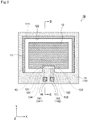
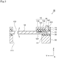
- Figs. 2 and 3 are a plan view and a cross-sectional view of the differential pressure detection element in the embodiment.
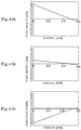
- Figs. 4(a) and 4(b) are graphs illustrating the warp amount of the differential pressure detection element in the embodiment
- Fig. 4(c) is a graph illustrating the warp amount of a differential pressure detection element in the related art.
- the differential pressure detection element 10 is an MEMS (Micro Electro Mechanical Systems) element configured to include a support substrate 11, a cantilever portion 12, a diffusion layer 13, a first insulating layer 14, a second insulating layer 15, and wiring portions 16 and 17.
- the support substrate 11 in the embodiment corresponds to an example of a support portion in the invention.
- the support substrate 11 and the cantilever portion 12 are integrally formed by processing an SOI (Silicon on Insulator) wafer 30.
- the support substrate 11 is configured as a laminate including a first silicon layer 31, a silicon oxide layer 32, and a second silicon layer 33.
- a rectangular opening 111 penetrating the support substrate 11 is formed on the support substrate 11.
- the cantilever portion 12 includes only the first silicon layer 31.
- the cantilever portion 12 is supported in a cantilever manner by the support substrate 11 at the fixed end 121 of the cantilever portion 12 so as to protrude into the opening 111 of the support substrate 11. Therefore, except for the fixed end 121 of the cantilever portion 12, a gap 122 is secured between the outer edge of the cantilever portion 12 and the inner wall surface of a through-hole 111.
- the gap 122 has a width of, for example, about 1 ⁇ m to 100 ⁇ m.
- the diffusion layer 13 includes piezoresistive portions 131 and 132 and lead portions 133 to 135.
- a pair of the piezoresistive portions 131 and 132 is electrically connected in series to the wiring portions 16 and 17 described later by the lead portions 133 to 135.
- the piezoresistive portions 131 and 132 are formed by doping the first silicon layer 31 (n-type semiconductor) with p-type impurities.
- the piezoresistive portions 131 and 132 are provided at the fixed end 121 where the stress is at maximum in the cantilever portion 12 at the time of pressure application.
- the resistance values of the piezoresistive portions 131 and 132 are changed in accordance with the elastic deformation of the cantilever portion 12.
- the wiring portions 133 to 135 of the diffusion layer 13 are also formed by doping the first silicon layer 31 with p-type impurities.
- the impurity concentration in the lead portions 133 to 135 is higher than the impurity concentration in the piezoresistive portions 131 and 132.
- the piezoresistive portions 131 and 132 of the diffusion layer 13 are composed of a p - type semiconductor
- the lead portions 133 to 135 of the diffusion layer 13 are composed of a p + type semiconductor.
- the electrical resistance values of the piezoresistive portions 131 and 132 are higher than the electrical resistance values of the lead portions 133 to 135.
- the first lead portion 133 electrically connects one end (upper end in Fig. 2 ) of the one piezoresistive portion 131 and one end (upper end in Fig. 2 ) of the other piezoresistive portion 132.
- the second lead portion 134 electrically connects the other end (lower end in Fig. 2 ) of the one piezoresistive portions 131 and the first wiring portion 16.
- the third lead portion 135 electrically connects the other end (the lower end in Fig. 2 ) of the other piezoresistive portion 132 and the second wiring portion 17.
- the diffusion layer 13 may be formed by doping the first silicon layer 31 (p-type semiconductor) with n-type impurities.
- the piezoresistive portions 131 and 132 are composed of an n - type semiconductor
- the wiring portions 133 to 135 are composed of an n + type semiconductor.
- the diffusion layer 13 is covered with the first insulating layer 14, so that electrical insulation properties of the piezoresistive portions 131 and 132, the lead portions 133 to 135, and the wiring portions 16 and 17 are secured.
- the first insulating layer 14 is configured as a layer having a linear expansion coefficient smaller than the linear expansion coefficient of silicon, and specifically, the first insulating layer is configured as a silicon oxide (SiO 2 ) layer.
- the first insulating layer 14 has a thickness w 1 of, for example, about 0.5 nm to 200 nm.
- the first insulating layer 14 is formed on the fixed end 121 of the cantilever portion 12 including the diffusion layer 13 and the support substrate 11.
- the second insulating layer 15 is laid on the first insulating layer 14.
- the second insulating layer 15 is configured as a layer having a linear expansion coefficient larger than the linear expansion coefficient of the first insulating layer 14, and specifically, the second insulating layer configured as a silicon nitride (SiN) layer.
- the second insulating layer 15 has a thickness w 2 of, for example, about 3 nm to 100 nm.
- the cantilever is greatly contracted in comparison with the insulating film. Therefore, the cantilever warps to the side opposite to the insulating film in the differential pressure detection element having a structure in the related art that has no second insulating layer. If the cantilever greatly warps in the offset state as described above, a large initial stress occurs in the piezoresistive portions formed at the base of the cantilever, so that the offset voltage (the output voltage of the differential pressure detection element in the offset state) increases. As the offset voltage increases, in some cases, the correction of the output of the differential pressure detection element or the like is adversely affected, so that the detection accuracy of the differential pressure detection element is deteriorated.
- the second insulating layer 15 is laid on the first insulating layer 14, and the linear expansion coefficient of the second insulating layer 15 is set to be larger than the linear expansion coefficient of the first insulating layer 14. Therefore, in the cooling process after the formation of the second insulating layer 15, the second insulating layer 15 is also greatly contracted in comparison with the first insulating layer 14. As a result, the warp of the cantilever portion 12 can be canceled out, so that the offset voltage of the differential pressure detection element 10 can be reduced.
- the relationship between the thickness w 1 of the first insulating layer 14 and the thickness w 2 of the second insulating layer 15 satisfies the following Mathematical Formula (3). Therefore, the warp of the cantilever portion 12 can be more appropriately canceled out by the second insulating layer 15, and the symmetry of the sensitivity of the differential pressure detection element 10 with respect to the pressure application direction can be further improved.
- Mathematical Formula (3) 0 ⁇ w 2 w 1 ⁇ 1 2
- a differential pressure detection element having a structure in the related art that has a silicon oxide layer with a thickness of 200 nm and has no silicon nitride layer
- the distal end of the cantilever portion is warped by about 6 ⁇ m in the -Z direction.
- the vertical axis represents a displacement amount along the Z axis (refer to Figs. 2 and 3 ) of the cantilever portion 12 in the offset state.
- the horizontal axis represents the distance from the distal end of the cantilever portion 12 along the -Y direction (refer to Figs. 2 and 3 ).
- the first wiring portion 16 is provided on the upper surface 112 of the support substrate 11 through the openings 141 and 151 of the first and second insulating layers 14 and 15 so as to be in contact with the end portion (lower end in Fig. 2 ) of the second lead portion 134 and is electrically connected to the second lead portion 134.
- the second wiring portion 17 is also provided on the upper surface 112 of the support substrate 11 through the openings 142 and 152 of the first and second insulating layers 14 and 15 so as to be in contact with the end portion (lower end in Fig. 2 ) of the third lead portion 135 and is electrically connected to the third lead portion 135.
- the wiring portions 16 and 17 are electrically connected to the above-described flow rate calculation unit 20 through wiring portions or the like not illustrated in particular.
- a bridge circuit may be configured by using wiring portions, lead portion, and piezoresistive portions. In this case, a small change in resistance value can be extracted as a large output.
- the above-described differential pressure detection element 10 is installed in the bypass passage 4 so that the extending direction of the cantilever portion 12 is substantially perpendicular to the extending direction of the bypass passage 4 (that is, the flowing direction of the fluid in the bypass passage 4) and the axial direction of the opening 111 of the support substrate 11 is substantially parallel to the extending direction of the bypass passage 4.
- the bypass passage 4 is bent midway, the shape of the bypass passage 4 is not particularly limited thereto.
- the bypass passage 4 may have a shape where the bypass passage is not bent midway.
- Fig. 5 is a diagram illustrating a modified example of the bypass passage 4.
- the gap 122 of the differential pressure detection element 10 is narrowed to such a degree that almost no fluid flows. Therefore, the pressure of the upstream opening 5 is applied to the upstream side of the cantilever portion 12, whereas the pressure of the downstream opening 6 is applied to the downstream side of the cantilever portion 12.
- the cantilever portion 12 of the differential pressure detection element 10 is elastically deformed in accordance with the pressure difference between the openings 5 and 6, and thus, distortion occurs in the piezoresistive portions 131 and 132.
- the flow rate calculation unit 20 detects changes in the resistance values of the piezoresistive portions 131 and 132 corresponding to the differential pressure through the wiring portions 16 and 17.
- the flow rate calculation unit 20 calculates the flow rate of the fluid on the basis of the differential pressure in the main flow passage 2 by using the fact that there is a correlation between the pressure loss of the fluid and the flow rate.
- the flow rate calculation unit 20 can be configured with, for example, a computer, an analog circuit, or the like.
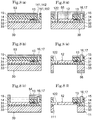
- Fig. 6 is a flowchart illustrating the method of manufacturing the differential pressure detection element in the embodiment, and Figs. 7(a) to 8(f) are cross-sectional views illustrating the steps of Fig. 6 .
- an SOI wafer 30 is prepared.
- the SOI wafer 30 is configured to include a first silicon layer 31 (active layer), a silicon oxide layer 32 (BOX (Buried Oxide) layer), and a second silicon layer 33 (handle layer).
- the three layers 31 to 33 are laminated so that the silicon oxide layer 32 is interposed between the two silicon layers 31 and 33.
- the SOI wafer 30 in the embodiment corresponds to an example of the SOI substrate in the invention.
- a method of forming the SOI wafer 30 there may be exemplified a method of bonding another silicon substrate to a silicon substrate having a silicon oxide layer formed thereon, an SIMOX (Separation by Implanted Oxygen) method, a smart cut method, or the like.
- SIMOX Separatation by Implanted Oxygen
- a diffusion layer 13 is formed in the first silicon layer 31 of the SOI wafer 30.
- a thermal oxidation process is performed on the SOI wafer 30 to form a thermal silicon oxide layer 41 in the first silicon layer 31.
- the thermal silicon oxide layer 41 constitutes a portion of the above-described first insulating layer 16.
- the thermal silicon oxide layer 41 has a function of suppressing channeling of ions during ion implantation at the time of forming the diffusion layer 13 and a function of suppressing outward diffusion of ions during annealing after the ion implantation.
- a first resist layer 51 is formed on the thermal silicon oxide layer 41.
- the first resist layer 51 has openings corresponding to the shapes of the lead portions 133 to 135 of the diffusion layer 13.
- the lead portions 133 to 135 are formed by doping the first silicon layer 31 with p-type impurities through the opening of the first resist layer 51, and after that, the first resist layer 51 is removed.
- a second resist layer 52 is formed on the SOI wafer 30.
- the second resist layer 52 has openings corresponding to the shape of the entire diffusion layer 13 including the piezoresistive portions 131 and 132.
- the first silicon layer 31 is doped with p-type impurities through the opening of the second resist layer 52 to form the piezoresistive portions 131 and 132, and after that, the second resist layer 52 is removed.
- ion implantation method As a method of doping the first silicon layer 31 of the SOI wafer 30 with impurities, there are exemplified an ion implantation method and the like. At this time, ion implantation is controlled so that the impurity concentration in the wiring portions 133 to 135 is higher than the impurity concentration in the piezoresistive portions 131 and 132.
- a first insulating layer 14 covering the diffusion layer 13 is formed on the entire surface of the SOI wafer 30.
- a silicon oxide film is further deposited on the thermal silicon oxide layer 41 by a CVD (Chemical Vapor Deposition) method to form a deposited silicon oxide layer 42.
- CVD Chemical Vapor Deposition
- an annealing process is performed on the thermal silicon oxide layer 41 and the deposited silicon oxide layer 42 that are laminated on each other to integrate the two silicon oxide layers 41 and 42, so that the first insulating layer 14 is formed.
- the temperature is increased up to about 900°C to 1200°C.
- the temperature of the annealing process corresponds to an example of the layer formation temperature of the first insulating layer in the invention.
- step S14 of Fig. 6 by depositing a silicon nitride film on the first insulating layer 14 by LPCVD (Low Pressure Chemical Vapor Deposition) method, the second insulating layer 15 is formed.
- the temperature is increased up to, for example, about 500°C to 800°C.
- the temperature of the LPCVD method corresponds to an example of the layer formation temperature of the second insulating layer in the invention.
- ⁇ 0 is a linear expansion coefficient of the material of which the cantilever portion 12 is composed
- ⁇ 1 is a linear expansion coefficient of the first insulating layer 14
- v 1 is a Poisson's ratio of the first insulating layer 14
- E 1 is a Young's modulus of the first insulating layer 14
- dT 1 is a temperature difference in the cooling process after the formation of the first insulating layer 14 (that is, a difference between the maximum temperature in the annealing process in step S13 described above and the room temperature).
- a thermal stress ⁇ 2 occurring in the second insulating layer 15 can be expressed by the following Mathematical Formula (5).
- ⁇ 2 is a linear expansion coefficient of the second insulating layer 15
- v 2 is a Poisson's ratio of the second insulating layer 15
- E 2 is a Young's modulus of the second insulating layer 15
- dT 2 is a temperature difference in the cooling process after the formation of the second insulating layer 15 (that is, a difference between the maximum temperature in the LPCVD method in step S14 described above and the room temperature).
- the above-described steps S13 and S14 are executed so as to satisfy the following Mathematical Formula (7) on the basis of the above-described Mathematical Formulas (3) to (6).
- the warp of the cantilever portion 12 can be more appropriately canceled out by the second insulating layer 15, and thus, the symmetry of the sensitivity of the differential pressure detection element 10 in the pressure application direction can be further improved.
- Mathematical Formula (7) 0 ⁇ w 2 w 1 ⁇ E 1 1 ⁇ v 2 ⁇ 1 ⁇ ⁇ 0 d T 1 E 2 1 ⁇ v 1 ⁇ 2 ⁇ ⁇ 1 d T 2 ⁇ 2
- the thickness w 1 of the first insulating layer 14 in the above-described Mathematical Formulas (6) and (7) is defined as a sum of the thickness of the thermal silicon oxide layer 41 formed in the above-described step S12 and the thickness of the deposited silicon oxide layer 42 formed in the above-described step S13.
- step S15 of Fig. 6 wiring portions 16 and 17 are formed.
- a third resist layer 53 is formed on the second insulating layer 15.
- the third resist layer 53 has openings corresponding to the shapes of the wiring portions 16 and 17.
- an etching process is performed on the first and second insulating layers 14 and 15 through the opening of the third resist layer 53. Therefore, the opening 141, 142, 151, and 152 of the first and second insulating layers 14 and 15 are formed.
- the openings 141, 142, 151, and 152 of the first and second insulating layers 14 and 15 are filled with a conductive material, and after that, the third resist layer 53 is removed.
- the wiring portions 16 and 17 are formed.
- a conductive material there may be exemplified a metal material such as copper, aluminum, and gold.
- a method of filling with the conductive material there may be exemplified sputtering, vacuum deposition, plating, and the like.
- step S16 of Fig. 6 the cantilever portion 12 is formed.
- a fourth resist layer 54 is formed on the second insulating layer 15 and the wiring portions 16 and 17.
- the fourth resist layer 54 has an opening corresponding to a region including the cantilever portion 12 excluding the fixed end 121 in the first silicon layer 31.
- a fifth resist layer 55 is formed on the first silicon layer 31, the second insulating layer 15, and the wiring portions 16 and 17.
- the fifth resist layer 55 has an opening corresponding to the shape of the above-described gap 122 between the support substrate 11 and the cantilever portion 12.
- the cantilever portion 12 is defined by the gap 122.
- the silicon oxide layer 32 of the SOI wafer 30 functions as an etching stopper.
- step S17 of Fig. 6 the support substrate 11 is formed.
- a sixth resist layer 56 is formed on the lower surface of the SOI wafer 30.
- the sixth resist layer 56 has an opening corresponding to the shape of the opening 111 of the above-described support substrate 11.
- an etching process is performed on the second silicon layer 33 from the lower side.
- the silicon oxide layer 32 of the SOI wafer 30 functions as an etching stopper.
- an etching process is performed on the silicon oxide layer 32 from the lower side to form the support substrate 11 having the opening 111.
- step S18 of Fig. 6 the individual differential pressure detection elements 10 are achieved by dicing the multiple differential pressure detection elements 10 in the form of individual pieces.
- the second insulating layer 15 is laid on the first insulating layer 14, and the linear expansion coefficient of the second insulating layer 15 is set to be larger than the linear expansion coefficient of the first insulating layer 14. Therefore, the warp of the cantilever portion 12 can be canceled out, and thus, the offset voltage of the differential pressure detection element 10 can be reduced.
- the silicon nitride layer 15 is laid on the silicon oxide layer 14, it is possible to prevent the phenomenon that the cantilever portion is deflected as time elapses due to penetration of moisture into the silicon oxide layer and expansion of the silicon oxide layer,. As a result, for example, it is possible to prevent the position of the cantilever portion 12 in the offset state from changing with time.
- step S12 of Fig. 6 in the embodiment corresponds to an example of a first step in the invention
- step S13 of Fig. 6 in the embodiment corresponds to an example of a second step in the invention
- step S14 of Fig. 6 in the embodiment corresponds to an example of a third step in the invention.
- the first insulating layer 14 is formed by annealing the two layers of the thermal silicon oxide layer 41 formed by the thermal oxidation process and the deposited silicon oxide layer 42 formed by the CVD method.
- the method of forming the first insulating layer 14 is not particularly limited thereto.
- the first insulating layer 14 may be configured with a single layer of a silicon oxide layer formed by any of a thermal oxidation method, a CVD method, a spin coating method, or the like.
Landscapes
- Physics & Mathematics (AREA)
- General Physics & Mathematics (AREA)
- Engineering & Computer Science (AREA)
- Fluid Mechanics (AREA)
- Microelectronics & Electronic Packaging (AREA)
- Mechanical Engineering (AREA)
- Computer Hardware Design (AREA)
- Manufacturing & Machinery (AREA)
- Measuring Fluid Pressure (AREA)
- Pressure Sensors (AREA)
- Measuring Volume Flow (AREA)
- Micromachines (AREA)
Applications Claiming Priority (2)
| Application Number | Priority Date | Filing Date | Title |
|---|---|---|---|
| JP2016047102A JP6073512B1 (ja) | 2016-03-10 | 2016-03-10 | 差圧検出素子、流量計測装置、及び、差圧検出素子の製造方法 |
| PCT/JP2017/003593 WO2017154424A1 (ja) | 2016-03-10 | 2017-02-01 | 差圧検出素子、流量計測装置、及び、差圧検出素子の製造方法 |
Publications (2)
| Publication Number | Publication Date |
|---|---|
| EP3428601A1 true EP3428601A1 (de) | 2019-01-16 |
| EP3428601A4 EP3428601A4 (de) | 2019-10-16 |
Family
ID=57937644
Family Applications (1)
| Application Number | Title | Priority Date | Filing Date |
|---|---|---|---|
| EP17762769.2A Withdrawn EP3428601A4 (de) | 2016-03-10 | 2017-02-01 | Differenzdruckerfassungselement, durchflussmessvorrichtung und verfahren zur herstellung des differenzdruckerfassungselements |
Country Status (4)
| Country | Link |
|---|---|
| US (1) | US10175073B2 (de) |
| EP (1) | EP3428601A4 (de) |
| JP (1) | JP6073512B1 (de) |
| WO (1) | WO2017154424A1 (de) |
Families Citing this family (4)
| Publication number | Priority date | Publication date | Assignee | Title |
|---|---|---|---|---|
| CN105241600B (zh) * | 2015-08-17 | 2017-12-29 | 中国科学院地质与地球物理研究所 | 一种mems压力计芯片及其制造工艺 |
| US10684159B2 (en) * | 2016-06-27 | 2020-06-16 | Applied Materials, Inc. | Methods, systems, and apparatus for mass flow verification based on choked flow |
| JP6652479B2 (ja) * | 2016-10-14 | 2020-02-26 | 株式会社フジクラ | 差圧検出素子及び流量計測装置 |
| US10809139B2 (en) * | 2018-02-14 | 2020-10-20 | Carefusion 303, Inc. | Integrated sensor to monitor fluid delivery |
Family Cites Families (17)
| Publication number | Priority date | Publication date | Assignee | Title |
|---|---|---|---|---|
| WO2007061047A1 (ja) * | 2005-11-25 | 2007-05-31 | Matsushita Electric Works, Ltd. | ウェハレベルパッケージ構造体およびその製造方法 |
| JP4739164B2 (ja) * | 2006-10-20 | 2011-08-03 | 三菱電機株式会社 | 車両用エンジンの吸入空気圧力測定用の半導体感歪センサ |
| CN101837943B (zh) * | 2009-10-30 | 2011-11-09 | 北京工业大学 | 定量测试力电性能与显微结构的传感器及制作方法 |
| JP5445196B2 (ja) * | 2010-02-10 | 2014-03-19 | セイコーエプソン株式会社 | 応力検出素子、触覚センサー、および把持装置 |
| WO2011119930A1 (en) * | 2010-03-26 | 2011-09-29 | Wayne State University | Resonant sensor with asymmetric gapped cantilevers |
| IT1402181B1 (it) * | 2010-09-13 | 2013-08-28 | Fond Istituto Italiano Di Tecnologia | Dispositivo microelettromeccanico elettro-attivo e relativo procedimento di rivelazione |
| JP5656191B2 (ja) * | 2011-01-07 | 2015-01-21 | 国立大学法人 東京大学 | 流速センサ |
| EP2669648A4 (de) * | 2011-01-28 | 2017-03-01 | The University of Tokyo | Differenzdrucksensor |
| JP5867821B2 (ja) * | 2012-03-08 | 2016-02-24 | セイコーインスツル株式会社 | 圧力センサ |
| JP5867820B2 (ja) * | 2012-03-08 | 2016-02-24 | セイコーインスツル株式会社 | 圧力センサ |
| JP5778619B2 (ja) * | 2012-05-02 | 2015-09-16 | セイコーインスツル株式会社 | 圧力センサ |
| JP6068168B2 (ja) * | 2013-01-31 | 2017-01-25 | 株式会社フジクラ | 差圧検出素子 |
| JP6041308B2 (ja) * | 2013-03-08 | 2016-12-07 | セイコーインスツル株式会社 | 圧力センサ |
| JP6087735B2 (ja) * | 2013-06-06 | 2017-03-01 | 株式会社フジクラ | 流量センサ及び流量検出システム |
| JP6026963B2 (ja) * | 2013-06-24 | 2016-11-16 | 株式会社フジクラ | 流量センサ及び流量検出システム |
| US10393608B2 (en) * | 2014-06-25 | 2019-08-27 | Seiko Instruments Inc. | Pressure change measuring apparatus and pressure change measuring method |
| US9661411B1 (en) * | 2015-12-01 | 2017-05-23 | Apple Inc. | Integrated MEMS microphone and vibration sensor |
-
2016
- 2016-03-10 JP JP2016047102A patent/JP6073512B1/ja not_active Expired - Fee Related
-
2017
- 2017-02-01 US US15/557,018 patent/US10175073B2/en not_active Expired - Fee Related
- 2017-02-01 EP EP17762769.2A patent/EP3428601A4/de not_active Withdrawn
- 2017-02-01 WO PCT/JP2017/003593 patent/WO2017154424A1/ja not_active Ceased
Also Published As
| Publication number | Publication date |
|---|---|
| WO2017154424A1 (ja) | 2017-09-14 |
| US10175073B2 (en) | 2019-01-08 |
| JP2017161401A (ja) | 2017-09-14 |
| JP6073512B1 (ja) | 2017-02-01 |
| US20180245955A1 (en) | 2018-08-30 |
| EP3428601A4 (de) | 2019-10-16 |
Similar Documents
| Publication | Publication Date | Title |
|---|---|---|
| US10775248B2 (en) | MEMS strain gauge sensor and manufacturing method | |
| US10175073B2 (en) | Differential pressure detection element, flow rate measurement device, and method of manufacturing differential pressure detection element | |
| JP3344138B2 (ja) | 半導体複合センサ | |
| TWI506278B (zh) | High Voltage Resistive MEMS Sensors | |
| EP3581903B1 (de) | Elektrische n-implantat-abschirmung für einen piezowiderstandssensor | |
| EP2878940B1 (de) | MEMS-Drucksensor-Feldabschirmungslayout für Oberflächenladungsimmunität in ölgefülltem Gehäuse | |
| US9557237B2 (en) | MEMS pressure sensor field shield layout for surface charge immunity in oil filled packaging | |
| US20150008544A1 (en) | Physical quantity sensor | |
| KR102278929B1 (ko) | 피에조 저항형 센서 | |
| EP3832279B1 (de) | Halbleiterbelastungssensor | |
| CN107449538A (zh) | 半导体压力传感器 | |
| US8171806B2 (en) | Force detection element | |
| CN113252216A (zh) | 一种mems压力传感器及其的制作方法 | |
| JP6652479B2 (ja) | 差圧検出素子及び流量計測装置 | |
| US7666699B2 (en) | Semiconductor strain gauge and the manufacturing method | |
| CN109932108A (zh) | 压力传感器 | |
| JP2015194443A (ja) | 差圧検出素子の製造方法 | |
| CN104111132B (zh) | 半导体器件及其制造方法 | |
| EP2597433A1 (de) | Wärmeluftstrommengensensor | |
| WO2023176082A1 (ja) | Memsセンサ | |
| WO2026086009A1 (zh) | 压力传感器芯片及其制备方法、压力传感器 | |
| JP6785689B2 (ja) | 圧力センサ | |
| JP2009069030A (ja) | 圧力検出素子 | |
| JPH04286166A (ja) | 半導体加速度センサ | |
| JP2005333093A (ja) | 半導体抵抗素子及びその製造方法並びに半導体抵抗素子を用いた半導体装置 |
Legal Events
| Date | Code | Title | Description |
|---|---|---|---|
| STAA | Information on the status of an ep patent application or granted ep patent |
Free format text: STATUS: THE INTERNATIONAL PUBLICATION HAS BEEN MADE |
|
| PUAI | Public reference made under article 153(3) epc to a published international application that has entered the european phase |
Free format text: ORIGINAL CODE: 0009012 |
|
| STAA | Information on the status of an ep patent application or granted ep patent |
Free format text: STATUS: REQUEST FOR EXAMINATION WAS MADE |
|
| 17P | Request for examination filed |
Effective date: 20170922 |
|
| AK | Designated contracting states |
Kind code of ref document: A1 Designated state(s): AL AT BE BG CH CY CZ DE DK EE ES FI FR GB GR HR HU IE IS IT LI LT LU LV MC MK MT NL NO PL PT RO RS SE SI SK SM TR |
|
| AX | Request for extension of the european patent |
Extension state: BA ME |
|
| DAV | Request for validation of the european patent (deleted) | ||
| DAX | Request for extension of the european patent (deleted) | ||
| A4 | Supplementary search report drawn up and despatched |
Effective date: 20190918 |
|
| RIC1 | Information provided on ipc code assigned before grant |
Ipc: G01L 13/06 20060101AFI20190912BHEP Ipc: B81B 3/00 20060101ALI20190912BHEP Ipc: G01F 1/34 20060101ALI20190912BHEP Ipc: B81C 1/00 20060101ALI20190912BHEP Ipc: H01L 29/84 20060101ALI20190912BHEP Ipc: G01L 9/00 20060101ALI20190912BHEP |
|
| STAA | Information on the status of an ep patent application or granted ep patent |
Free format text: STATUS: THE APPLICATION IS DEEMED TO BE WITHDRAWN |
|
| 18D | Application deemed to be withdrawn |
Effective date: 20200603 |