EP3425355B1 - Fourier transform infrared spectrophotometer - Google Patents
Fourier transform infrared spectrophotometer Download PDFInfo
- Publication number
- EP3425355B1 EP3425355B1 EP18182122.4A EP18182122A EP3425355B1 EP 3425355 B1 EP3425355 B1 EP 3425355B1 EP 18182122 A EP18182122 A EP 18182122A EP 3425355 B1 EP3425355 B1 EP 3425355B1
- Authority
- EP
- European Patent Office
- Prior art keywords
- voltage
- signal
- detector
- output voltage
- input
- Prior art date
- Legal status (The legal status is an assumption and is not a legal conclusion. Google has not performed a legal analysis and makes no representation as to the accuracy of the status listed.)
- Active
Links
Images


Classifications
-
- G—PHYSICS
- G01—MEASURING; TESTING
- G01J—MEASUREMENT OF INTENSITY, VELOCITY, SPECTRAL CONTENT, POLARISATION, PHASE OR PULSE CHARACTERISTICS OF INFRARED, VISIBLE OR ULTRAVIOLET LIGHT; COLORIMETRY; RADIATION PYROMETRY
- G01J3/00—Spectrometry; Spectrophotometry; Monochromators; Measuring colours
- G01J3/28—Investigating the spectrum
- G01J3/45—Interferometric spectrometry
-
- G—PHYSICS
- G01—MEASURING; TESTING
- G01N—INVESTIGATING OR ANALYSING MATERIALS BY DETERMINING THEIR CHEMICAL OR PHYSICAL PROPERTIES
- G01N21/00—Investigating or analysing materials by the use of optical means, i.e. using sub-millimetre waves, infrared, visible or ultraviolet light
- G01N21/17—Systems in which incident light is modified in accordance with the properties of the material investigated
- G01N21/25—Colour; Spectral properties, i.e. comparison of effect of material on the light at two or more different wavelengths or wavelength bands
- G01N21/31—Investigating relative effect of material at wavelengths characteristic of specific elements or molecules, e.g. atomic absorption spectrometry
- G01N21/35—Investigating relative effect of material at wavelengths characteristic of specific elements or molecules, e.g. atomic absorption spectrometry using infrared light
-
- G—PHYSICS
- G01—MEASURING; TESTING
- G01J—MEASUREMENT OF INTENSITY, VELOCITY, SPECTRAL CONTENT, POLARISATION, PHASE OR PULSE CHARACTERISTICS OF INFRARED, VISIBLE OR ULTRAVIOLET LIGHT; COLORIMETRY; RADIATION PYROMETRY
- G01J3/00—Spectrometry; Spectrophotometry; Monochromators; Measuring colours
- G01J3/02—Details
-
- G—PHYSICS
- G01—MEASURING; TESTING
- G01J—MEASUREMENT OF INTENSITY, VELOCITY, SPECTRAL CONTENT, POLARISATION, PHASE OR PULSE CHARACTERISTICS OF INFRARED, VISIBLE OR ULTRAVIOLET LIGHT; COLORIMETRY; RADIATION PYROMETRY
- G01J3/00—Spectrometry; Spectrophotometry; Monochromators; Measuring colours
- G01J3/28—Investigating the spectrum
- G01J3/45—Interferometric spectrometry
- G01J3/453—Interferometric spectrometry by correlation of the amplitudes
- G01J3/4535—Devices with moving mirror
-
- G—PHYSICS
- G01—MEASURING; TESTING
- G01J—MEASUREMENT OF INTENSITY, VELOCITY, SPECTRAL CONTENT, POLARISATION, PHASE OR PULSE CHARACTERISTICS OF INFRARED, VISIBLE OR ULTRAVIOLET LIGHT; COLORIMETRY; RADIATION PYROMETRY
- G01J3/00—Spectrometry; Spectrophotometry; Monochromators; Measuring colours
- G01J3/28—Investigating the spectrum
- G01J3/45—Interferometric spectrometry
- G01J3/453—Interferometric spectrometry by correlation of the amplitudes
- G01J2003/4538—Special processing
-
- G—PHYSICS
- G01—MEASURING; TESTING
- G01N—INVESTIGATING OR ANALYSING MATERIALS BY DETERMINING THEIR CHEMICAL OR PHYSICAL PROPERTIES
- G01N21/00—Investigating or analysing materials by the use of optical means, i.e. using sub-millimetre waves, infrared, visible or ultraviolet light
- G01N21/17—Systems in which incident light is modified in accordance with the properties of the material investigated
- G01N21/25—Colour; Spectral properties, i.e. comparison of effect of material on the light at two or more different wavelengths or wavelength bands
- G01N21/31—Investigating relative effect of material at wavelengths characteristic of specific elements or molecules, e.g. atomic absorption spectrometry
- G01N21/35—Investigating relative effect of material at wavelengths characteristic of specific elements or molecules, e.g. atomic absorption spectrometry using infrared light
- G01N2021/3595—Investigating relative effect of material at wavelengths characteristic of specific elements or molecules, e.g. atomic absorption spectrometry using infrared light using FTIR
Definitions
- the present invention relates to a Fourier transform infrared spectrophotometer (FTIR).
- FTIR Fourier transform infrared spectrophotometer
- an interferometer which includes a beam splitter, fixed mirror and movable mirror is used, such as a Michelson's interferometer.
- the position of the movable mirror is changed to change the optical length difference between a beam of light reflected by this movable mirror and a beam of light reflected by the fixed mirror, and thereby generate varying interfering light in which the two aforementioned beams of light interfere with each other having a phase difference which varies depending on the optical length difference.
- Infrared light having a wavelength width including an absorption wavelength of a target compound contained in a sample is introduced into the interferometer to generate interfering light.
- Fig. 2 shows the configuration of the main components of a conventionally used Fourier transform infrared spectrophotometer.
- the Fourier transform infrared spectrophotometer 100 is roughly composed of two sections: an interference section located within an airtight chamber 101 and a measurement section located outside the airtight chamber 101.
- the interference section includes a light source 102, condensng mirror 103, collimating mirror 104, beam splitter 105, fixed mirror 106, and movable mirror 107.
- the measurement section includes a parabolic mirror 112, sample chamber 113, ellipsoidal mirror 115, and detector 116.
- a sample 114 is placed within the sample chamber 113.
- Infrared light emitted from the light source 102 is cast onto the beam splitter 105 via the condensing mirror 103 and the collimating mirror 104.
- the beam splitter 105 splits the light into two beams travelling toward the fixed and movable mirrors 106 and 107, respectively.
- the infrared beams respectively reflected by the fixed and movable mirrors 106 and 107 return to the beam splitter 105 and are merged into a single beam.
- This beam exits from the window 108 of the airtight chamber 101 and travels toward the parabolic mirror 112. Being condensed by the parabolic mirror 112, the beam is cast into the sample 114 inside the sample chamber 113.
- the beam After passing through the sample 114, the beam is focused onto the detection surface of the detector 116 by the ellipsoidal mirror 115 and detected.
- Driving the movable mirror 107 back and forth (in the direction indicated by arrow M in Fig. 2 ) causes a change in the optical length difference between the infrared light reflected by the fixed mirror 106 and the infrared light reflected by the movable mirror 107.
- the two beams of infrared light interfere with each other having a phase difference which changes depending on the optical length difference.
- the interfering infrared light transmitted through the sample 114 is detected by the detector 116.
- An example of the detector 116 is a pyroelectric detector having a pyroelectric element and junction field-effect transistor.
- the pyroelectric element generates electric charges in an amount corresponding to the amount of incident infrared light and generates an electric current.
- the pyroelectric element is connected to the gate of the junction field-effect transistor, while a resistor is connected to the source of the same transistor.
- a change in voltage occurs at the gate to which the pyroelectric element is connected, causing a change in the amount of electric current flowing out of the source.
- This changes the potential difference between the two ends of the resistor connected to the source. By measuring this potential difference, a voltage value which corresponds to the amount of incident infrared light can be obtained.
- the optical length of the infrared light reflected by the movable mirror 107 is equal to that of the light reflected by the fixed mirror 106 when the movable mirror 107 is located at a specific position.
- the two reflected beams merged with each other at the beam splitter 105 are in phase at all wavelengths and strengthen each other, so that the infrared light with the highest intensity is detected.
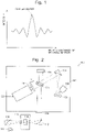
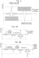
- a peak which corresponds to this state on the interferogram is called the "center burst" (see Fig. 1 ). This center burst corresponds to the highest peak which appears on the positive voltage side of the subtracted waveform indicated by the solid line in Fig. 3 .
- the beam splitter 105 consists of a pair of window members on which a thin layer of germanium (Ge) or similar material is deposited.
- Ge germanium
- the pair of window members are not uniform in thickness in the strict sense. Due to these factors, the two reflected beams of infrared light cannot be simultaneously in phase at all wavelengths. In some cases, the opposite situation occurs; i.e. the two reflected beams may have a phase difference of ⁇ at many wavelengths and weaken each other, causing the highest peak to appear in a downward-pointing form (i.e.
- the highest peak may appear on the negative voltage side). Even with the same apparatus, when a sample is placed inside, the highest peak can appear on either the positive or negative voltage side depending on the wavelength at which the strongest absorption by the sample occurs. When no sample is present, the peak pattern is always the same. Therefore, the height and direction (positive/negative) of the highest peak originating from the apparatus itself can be predicted to some extent for each individual apparatus. However, when a sample is present, it is impossible to predict which of the positive and negative voltage peaks will appear.
- the amplification factor of the amplifier is set so that the peak will certainly fall within the input range of the analogue-to-digital (A/D) converter, whichever of the two kinds of peaks appears.
- the highest peak only appears on either the positive voltage side or negative voltage side. If the highest peak appears on the positive voltage side as in the subtracted waveform indicated by the solid line in Fig. 3 , a considerable portion of the input range on the negative voltage side remains unused.
- the problem to be solved by the present invention is to provide a Fourier transform infrared spectrophotometer which can efficiently use the input range of the A/D converter regardless of whether the highest peak with a positive voltage or one with a negative voltage appears.
- a Fourier transform infrared spectrophotometer developed for solving the previously described problem includes:
- An example of the detector is a pyroelectric detector.
- the pyroelectric detector generates a voltage with a magnitude corresponding to the intensity of the interfering light and outputs a voltage obtained by subtracting a direct voltage with a predetermined magnitude (offset voltage) from the aforementioned voltage.
- a device which outputs a voltage obtained by subtracting, from a voltage with a magnitude corresponding to the intensity of the interfering light the direct-current (DC) component of the same voltage may also be used as the detector.
- a mercury cadmium telluride (MCT) detector or indium gallium arsenide (InGaAs) detector can be used, both of which are quantum detectors.
- the DC component corresponds to the component which contains no information on the frequency components that form an absorption spectrum obtained through the Fourier transform.
- the value of the voltage which is generated when the infrared light emitted from the light source is detected without interference can be used as the DC component.
- a calculated value based on the intensity of the infrared light emitted from the light source and the magnitude of the absorption of light by optical components included in the interferometer and other related sections may also be used.
- the judgment by the judging section can be made by checking whether or not the output signal from the A/D converter is a saturated signal.
- the first signal-processing operation in which an output voltage from the detector is amplified after the addition of a bias voltage
- the second signal-processing operation in which the same output voltage from the detector is amplified after the inversion of its polarity and the addition of the bias voltage
- the first signal-processing operation as shown in Fig. 4A , the voltage signal is initially shifted toward the negative side by the addition of the bias voltage.
- the voltage signal is amplified. Since the voltage signal has been shifted by the addition of the bias voltage in such a manner as to decrease the absolute value of the highest peak, the voltage signal falls within the input range of the A/D converter even after the amplification.
- the second signal-processing operation which includes polarity inversion, as shown in Fig. 4B , the highest peak becomes even higher due to the addition of the bias voltage (i.e. its absolute value increases) and is subsequently amplified by the amplifier. Consequently, the voltage signal goes beyond the input range of the A/D converter after the amplification, and a saturation signal is outputted.
- the judging section designates the first signal-processing operation as the processing method to be used in the actual measurement. Conversely, if the highest peak of the subtracted waveform is present on the negative voltage side, the voltage signal in the first signal-processing operation goes beyond the input range of the A/D converter after the amplification, while the voltage signal in the second signal-processing operation falls within the input range of the A/D converter after the amplification. Accordingly, the second signal-processing operation is designated as the processing method to be used in the actual measurement.
- the operation of amplifying the voltage signal is performed after the subtracted waveform biased toward the positive or negative voltage side is converted into a waveform which is evenly divided on both sides by being entirely shifted in a direction which decreases the height of the highest peak. Therefore, the input range of the A/D converter can be efficiently utilized on both positive and negative voltage sides.
- a Fourier transform infrared spectrophotometer includes:
- the subtracted waveform is entirely shifted by the fourth signal-processing operation when the highest peak is present on the positive voltage side, or by the third signal-processing operation when the highest peak is present on the negative voltage side, in such a manner as to decrease the height of the peak, whereby the waveform biased toward the positive or negative voltage side is converted into a waveform which is evenly divided on both sides. Therefore, the input range of the A/D converter can be efficiently utilized on both positive and negative voltage sides, as with the Fourier transform infrared spectrophotometer according to the first aspect of the present invention.
- a Fourier transform infrared spectrophotometer includes:
- the high-pass filter allows the passage of such frequency components of the output voltage from the detector that are equal to or higher than a predetermined frequency.
- High-pass filters are also known as differential circuits (for example, see Patent Literature 4).
- the predetermined frequency is set at a value near a dominant frequency in the subtracted waveform by using the high-pass filter. As a result, the subtracted waveform biased toward the positive or negative voltage side is converted by differentiation into a waveform which is almost evenly divided on both sides. Therefore, the input range of the AID converter can be efficiently utilized on both positive and negative voltage sides.
- the input range of the A/D converter can be efficiently used regardless of whether the highest peak with a positive voltage or one with a negative voltage appears.
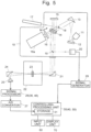
- Fig. 5 is a diagram showing the configuration which is common to the Fourier transform infrared spectrophotometers according to the first through third embodiments.
- the Fourier transform infrared spectrophotometer includes a main interferometer for obtaining an interferogram, and a control interferogram for controlling the sliding speed of the movable mirror as well as generating a timing signal used for the sampling of the signals obtained with the detector in the main interferometer.
- the main interferometer includes a light source 11, condensing mirror 12, collimating mirror 13, beam splitter 14, fixed mirror 15 and movable mirror 16. This interferometer generates interfering infrared light used for performing a spectral measurement.
- Infrared light emitted from the light source 11 is cast onto the beam splitter 14 via the condensing mirror 12 and the collimating mirror 13.
- the beam splitter 14 splits the light into two beams travelling toward the fixed and movable mirrors 15 and 16, respectively.
- the beams respectively reflected by the fixed and movable mirrors 15 and 16 once more meet at the beam splitter 14 and are thereby merged into a single beam.
- This beam is sent into an optical path leading to a parabolic mirror 21.
- the movable mirror 16 is driven back and forth (in the direction indicated by arrow M in Fig. 5 ) by a movable mirror driver 16a. Therefore, the combined beam becomes interfering light whose intensity temporally changes.
- This light is condensed by the parabolic mirror 21 and cast into a sample chamber 22. After passing through a sample 23 inside the sample chamber 22, the light is focused onto a detector 25 by an ellipsoidal mirror 24.
- the control interferometer includes a laser source 17, mirror 18, (aforementioned) beam splitter 14, (aforementioned) mirror 15 and (aforementioned) movable mirror 16.
- This interferometer generates interfering laser light for obtaining an interference fringe signal.
- the light emitted from the laser source 17 is cast onto the beam splitter 14 via the mirror 18 and becomes interfering light, as with the infrared light, which travels toward the parabolic mirror 21.
- This interfering laser light travels in the form of an extremely thin flux of light.
- This light is reflected by a mirror 19 placed in the optical path leading to the parabolic mirror 21. The reflected light enters a detector 20.
- the optical components constituting the main interferometer and the control interferometer are placed within an airtight chamber 10.
- the humidity within this chamber 10 is controlled. This is primarily aimed at protecting the beam splitter 14 and other optical elements whose substrates are made of potassium bromide (KBr), which is a deliquescent substance.
- the light-receiving signal from the detector 20, i.e. the interference fringe signal, is sent to a signal generator 29, which generates a pulsed signal used for performing the sampling of the light-receiving signal corresponding to the interfering infrared light.
- the laser-light interference fringe signal is also used for the slide control of the movable mirror 16.
- the detector 25 in the present embodiment is a pyroelectric detector having a pyroelectric element and junction field-effect transistor. This detector produces an output voltage having a positive or negative value which corresponds to the difference between the offset voltage of the junction field-effect transistor and the voltage corresponding to the amount of electric charges generated by the pyroelectric element according to the intensity of the infrared light.
- the light-receiving signal obtained in the detector 25 is processed by a signal processor 26 (36 or 46) in a characteristic manner as will be described later in the embodiments.
- the processed signal is converted into a digital signal by an analogue-to-digital (A/D) converter 27 and sent to a controlling-processing unit 30 (40 or 50).
- A/D analogue-to-digital
- a controlling-processing unit 30 40 or 50
- a Fourier transform computation is performed to create an absorption spectrum.
- the controlling-processing unit 30 may be constructed as a dedicated controlling-processing device equipped with a storage section 31. However, typically, this unit is actually a personal computer on which a dedicated controlling-processing software program is installed.
- An input unit 60 for allowing users to perform various input operations with a keyboard and pointing device (e.g. mouse), as well as a display unit 70, such as a liquid crystal display, for displaying measured results and other related information, are connected to the unit.
- Fig. 6 shows the configuration of the signal processor 26 and the controlling-processing unit 30 used in the Fourier transform infrared spectrophotometer according to the first embodiment.
- the signal processor 26 in the first embodiment includes: a polarity inverter 261 for outputting a voltage obtained by inverting the polarity of an input voltage; a bias voltage adder 262 for adding a bias voltage with a predetermined magnitude to an input voltage; and an amplifier 263 for amplifying an input voltage by a predetermined multiplying factor.
- the polarity inverter 261, bias voltage adder 262 and amplifier 263 each actually consist of electric circuits, in which the function of each component (which will be described later) is realized by an appropriate combination of various kinds of conventionally known electric circuits.
- the controlling-processing unit 30 includes a judging section 32 and a signal-processing determining section 33 as its functional blocks in addition to the storage section 31.
- those functional blocks are embodied by running a predetermined program previously installed on a computer used as the controlling-processing unit 30.
- a preliminary measurement for determining the signal-processing method to be used in a measurement of a real sample is performed in advance of the measurement.
- the preliminary measurement is performed by the controlling-processing unit 30 by operating each section of the Fourier transform infrared spectrophotometer, based on a command issued by a user through the input unit 60. It is also possible to configure the controlling-processing unit 30 to automatically perform the preliminary measurement when the Fourier transform infrared spectrometer is energized, or when a period of time equal to or longer than a predetermined length of time has passed since the previous measurement of a real sample.
- the intensity of the interfering infrared light incident on the detector 25 is sequentially measured.
- the preliminary measurement is performed two times; the first signal-processing operation is performed in the first measurement, and the second signal-processing operation is performed in the second measurement.
- the polarity inverter 261 does not invert the polarity of the output voltage received from the detector 25 but directly sends the voltage to the bias voltage adder 262 without inverting the polarity of the voltage.
- a signal-routing switch may be provided in front of the polarity inverter 261, and this switch may be used to directly send the voltage to the bias voltage adder 262, bypassing the polarity inverter 261.
- the bias voltage adder 262 adds a predetermined bias voltage to the sequentially inputted voltage and outputs the obtained voltage.
- the voltage obtained by the addition of the bias voltage is amplified by a predetermined multiplying factor in the amplifier 263 and outputted.
- the output voltage from the amplifier 263 is converted into a digital signal by the A/D converter 27 and stored in the storage section 31 in the controlling-processing unit 30.
- the polarity inverter 261 inverts the polarity of the output voltage received from the detector 25 and sends the voltage to the bias voltage adder 262.
- the bias voltage adder 262 adds a predetermined bias voltage to the sequentially inputted voltage with the inverted polarity and outputs the obtained voltage.
- the voltage obtained by the addition of the bias voltage is amplified by a predetermined multiplying factor in the amplifier 263 and outputted.
- the output voltage from the amplifier 263 is converted into a digital signal by the A/D converter 27 and stored in the storage section 31 in the controlling-processing unit 30.
- the first and second signal-processing operations differ from each other as to whether or not the inversion of the polarity of the output voltage from the detector 25 is performed.
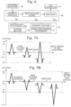
- Fig. 7 illustrates one example of a specific signal-processing operation, using a model of the subtracted waveform.
- the waveform is simplified for easier understanding of the feature of the signal-processing operation in the first embodiment.
- Subtracted waveforms obtained by actual measurements are more complex. The same also applies to the waveforms used for the explanation in the second and third embodiments.
- the subtracted waveform outputted from the detector 25 has the highest peak with an absolute voltage value of 4 V, and the largest output voltage on the opposite side to the polarity of the highest peak is 1 V. Based on this assumption, the bias voltage is set at -1.5 V, and the amplification factor is set at two.
- the input range of the A/D converter 27 is from -5 V to +5 V. It is impossible to predict whether the highest peak which appears on an interferogram ( Fig. 1 ) obtained with a Fourier transform infrared spectrophotometer will be pointed upward or downward (in other words, whether the highest peak will appear on the positive voltage side or on the negative voltage side in the subtracted waveform as shown in Fig. 3 ). However, since the magnitude of the highest peak (absolute voltage value) is almost constant, it is possible to previously estimate the range of the voltage which forms the subtracted waveform. Accordingly, based on this voltage range and the input range of the A/D converter 27, the magnitude of the bias voltage and the amplification factor can be determined beforehand.
- the range of the output voltage of the subtracted waveform is from - 1 V to +4 V.
- the subtracted waveform is processed as shown in Fig. 7A .
- the resulting output voltage of the amplifier 263 ranges from -5 V to +5 V, which falls within the input range of the AID converter 27.
- the subtracted waveform is processed as shown in Fig. 7B .
- the resulting output voltage of the amplifier 263 ranges from -11 V to -1 V, which goes beyond the input range of the A/D converter 27.
- the A/D converter 27 Upon receiving such an input voltage, the A/D converter 27 outputs a saturation signal, and this signal is stored in the storage section 31. Therefore, for each of the output voltages obtained through the first and second signal-processing operations, the judging section 32 can determine whether or not the output voltage is within the input range of the A/D converter 27, by checking whether nor not the corresponding signal stored in the storage 31 is saturated. After the determination by the judgement section 32, the signal-processing determining section 33 designates either the first or second signal-processing operation which has yielded the voltage that falls within the input range of the A/D converter 27 as the signal-processing method to be used in the actual measurement.
- the signal-processing determining section 33 designates the second signal-processing operation as the signal-processing method to be used in the actual measurement.
- the positive voltage used as the bias voltage in the previously described example may be replaced by a positive voltage having the same absolute value.
- Fig. 8 shows the configuration of the signal processor 36 and the controlling-processing unit 40 used in the Fourier transform infrared spectrophotometer according to the second embodiment.
- the signal processor 36 in the second embodiment includes: a bias voltage adder 362 for adding either a positive bias voltage or negative bias voltage to an input voltage, the two bias voltages having the same absolute value; and an amplifier 363 for amplifying an input voltage by a predetermined multiplying factor.
- the bias voltage adder 362 and amplifier 363 each actually consist of electric circuits, in which the function of each component (which will be described later) is realized by an appropriate combination of various kinds of conventionally known electric circuits.
- the controlling-processing unit 40 includes a judging section 42 and a signal-processing determining section 43 as its functional blocks in addition to the storage section 31.
- those functional blocks are embodied by running a predetermined program previously installed on a computer used as the controlling-processing unit 40.
- a preliminary measurement for determining the signal-processing method to be used in a measurement of a real sample is performed in advance of the measurement.
- the preliminary measurement is performed by the controlling-processing unit 40 by operating each section of the Fourier transform infrared spectrophotometer, based on a command issued by a user through the input unit 60. It is also possible to configure the controlling-processing unit 40 to automatically perform the preliminary measurement when the Fourier transform infrared spectrometer is energized, or when a period of time equal to or longer than a predetermined length of time has passed since the previous measurement of a real sample.
- the intensity of the interfering infrared light incident on the detector 25 is sequentially measured.
- the preliminary measurement is performed two times; the third signal-processing operation is performed in the first measurement, and the fourth signal-processing operation is performed in the second measurement.
- the bias voltage adder 362 adds a positive bias voltage to the voltage sequentially produced by the detector 25 and outputs the obtained voltage.
- the voltage obtained by the addition of the positive bias voltage is amplified by a predetermined multiplying factor in the amplifier 363 and outputted.
- the output voltage from the amplifier 363 is converted into a digital signal by the AID converter 27 and stored in the storage section 31 in the controlling-processing unit 40.
- the bias voltage adder 362 adds a negative bias voltage having the same absolute value as the aforementioned positive bias voltage to the voltage sequentially produced by the detector 25 and outputs the obtained voltage.
- the voltage obtained by the addition of the negative bias voltage is amplified by a predetermined multiplying factor in the amplifier 363 and outputted.
- the output voltage from the amplifier 363 is converted into a digital signal by the A/D converter 27 and stored in the storage section 31 in the controlling-processing unit 40.
- the third and fourth signal-processing operations differ from each other in the polarity of the bias voltage added to the output voltage of the detector 25 in the bias voltage adder 362.
- Fig. 9 illustrates one example of a specific signal-processing operation, using a model of the subtracted waveform. Similar to Fig. 7 , it is assumed that the subtracted waveform outputted from the detector 25 has the highest peak with an absolute voltage value of 4 V, and the largest output voltage on the opposite side to the polarity of the highest peak is 1 V. Based on this assumption, the bias voltage is set at ⁇ 1.5 V, and the amplification factor is set at two. The input range of the A/D converter 27 is from -5 V to +5 V. As already explained in the first embodiment, it is impossible to predict whether the highest peak will appear on the positive voltage side or on the negative voltage side in the subtracted waveform.
- the magnitude of the highest peak (absolute voltage value) is almost constant, it is possible to previously estimate the range of the voltage which forms the subtracted waveform and determine the magnitude of the bias voltage (absolute value). Based on this voltage range and the input range of the A/D converter 27, the magnitude of the bias voltage (absolute value) can be determined beforehand.
- the subtracted waveform is processed as shown in Fig. 9A .
- the resulting output voltage of the amplifier 363 ranges from +1 V to +11 V, which goes beyond the input range of the A/D converter 27.
- the subtracted waveform is processed as shown in Fig. 9B .
- the resulting output voltage from the amplifier 363 ranges from -5 V to +5 V, which falls within the input range of the A/D converter 27.
- the judging section 42 can determine whether or not the output voltage is within the input range of the A/D converter 27, by checking whether nor not the corresponding signal stored in the storage 31 is saturated.
- the signal-processing determining section 43 designates either the third or fourth signal-processing operation which has yielded the voltage that falls within the input range of the A/D converter 27 as the signal-processing method to be used in the actual measurement.
- the signal-processing determining section 43 designates the third signal-processing operation as the signal-processing method to be used in the actual measurement.
- Fig. 10 shows the configuration of the signal processor 46 and the controlling-processing unit 50 used in the Fourier transform infrared spectrophotometer according to the third embodiment.
- the signal processor 46 in the third embodiment includes: a high-pass filter (HPF) 464 for allowing the passage of only such frequency components of an input voltage signal that are equal to or higher than a predetermined frequency; and an amplifier 463 for amplifying an input voltage by a predetermined multiplying factor.
- the high-pass filter 464 and amplifier 463 each actually consist of electric circuits, in which the function of each component (which will be described later) is realized by an appropriate combination of various kinds of conventionally known electric circuits.
- the controlling-processing unit 50 has a storage section 31. However, this unit has neither the judging section nor the signal-processing determining section.
- no preliminary measurement is performed in the Fourier transform infrared spectrophotometer according to the third embodiment. Therefore, for example, after the device has been energized and necessary tasks (such as the optical path adjustment) have been performed, an actual measurement can be immediately performed. Needless to say, a preliminary measurement may be performed if it is necessary in order to determine the range of the frequency components to be allowed to pass through the high-pass filter 464, amplification factor, or input range of the A/D converter.
- Fig. 11 illustrates one example of a specific signal-processing operation, using a model of the subtracted waveform. Similar to Figs. 7 and 9 , it is assumed that the subtracted waveform outputted from the detector 25 has the highest peak with an absolute voltage value of 4 V, and the largest output voltage on the opposite side to the polarity of the highest peak is 1 V. Based on this assumption, the amplification factor is set at two. The input range of the A/D converter 27 is from -5 V to +5 V.
- the high-pass filter 464 is used to allow such frequency components of the output voltage from the detector that are equal to or higher than a predetermined frequency.
- the "predetermined" frequency may preferably be set at a value near the principal frequency in the subtracted waveform (or interferogram). This value depends on the wavelength at which a high-intensity emission is observed in the emission spectrum of the light source as well as the configuration of the optical system including the interferometer.
- the principal frequency in the subtracted waveform is determined by the speed of the movable mirror 16 and the wavelength of the infrared light.
- the wavelength of the infrared light is the wavelength of light absorbed by the target compound contained in the sample.
- a light source having a high emission intensity at that wavelength is used as the light source 11.
- the high-pass filter 464 is also known as a differential circuit.
- the subtracted waveform is differentiated by being passed through this high-pass filter 464.
- the waveform obtained by this differention is amplified by the amplifier 463 and subsequently converted into a digital signal by the A/D converter 27.
- Fig. 12 shows a simulated waveform obtained by passing a positive half-wave of a 1-kHz sinusoidal wave through a 1-kHz high-pass filter.
- the subtracted waveform biased toward the positive or negative voltage side is converted into a waveform which is (almost) evenly divided on both sides by the characteristic signal-processing operation of each embodiment. Therefore, unlike the conventional case, the input range of the A/D converter can be fully utilized without leaving a considerable portion of the input range unused on either the positive or negative voltage side on which the highest peak of the subtracted waveform does not appear. That is to say, the entire input range of the A/D converter can be efficiently used, and the bits of the input range can be maximally utilized, so that the measurement data can be acquired with a high level of resolving power.
- the conventional Fourier transform infrared spectrophotometer, the Fourier transform infrared spectrophotometers according to the first and second embodiments, and the Fourier transform infrared spectrophotometer according to the third embodiment are hereinafter compared in terms of the signal-to-noise (SN) ratio of a measurement signal obtained in each device.
- the conditions of the calculation are as follows:
- the signal has an SN ratio of one at the point of input into the signal processor in each device.
- the subtracted waveform inputted into the signal processor has the highest peak with a peak voltage (absolute value) of 4 V (i.e. +4 V or -4 V).
- the input range of the AID converter is from -5 V to +5 V.
- the amplification factor by the amplifier is set at 1.25 so that the highest peak will certainly fall within the input range of the AID converter (from -5 V to +5 V) regardless of whether the peak (with an absolute value of 4 V) appears on the positive voltage side or on the negative voltage side.
- the amplification factor of the signal in the amplifier 263 (363) is set at two.
- Vn(AD) represents characteristic noise of the A/D converter.
- This term is common to all of the Fourier transform infrared spectrophotometers of the conventional example and the first through third embodiments. Accordingly, it can be understood from the above table that the Fourier transform infrared spectrophotometers in the first and second embodiments have the highest SN ratio after the A/D conversion, followed by the third embodiment, and further by the conventional example.
- the Fourier transform infrared spectrophotometers according to the first and second embodiments can yield measurement data with a higher SN ratio than the Fourier transform infrared spectrophotometer according to the third embodiment.
- the Fourier transform infrared spectrometer according to the third embodiment has the advantage that it can be more easily constructed than the devices of the first and second embodiments, since the Fourier transform infrared spectrometers according to the first and second embodiments require the designing and addition of the circuits for the polarity conversion or the addition of bias voltage, whereas the Fourier transform infrared spectrometers according to the third embodiment utilizes the conventionally employed high-pass filter. Furthermore, the Fourier transform infrared spectrometers according to the third embodiment allows for the simplification of the measurement procedure, since it does not require preliminary measurements for determining the signal-processing method before the measurement of an actual sample.
- the previously described embodiments are mere examples and can be appropriately changed within the spirit of the present invention.
- the configuration of the Fourier transform infrared spectrophotometer shown in Fig. 5 as the common configuration to the first through third embodiments is a mere example.
- the signal-processing methods described in the first through third embodiments can be applied in various other devices which can similarly perform Fourier transform infrared spectrometry.
- one subtracted waveform is initially obtained by performing the first (or third) signal-processing operation while gradually changing the position of the movable mirror 16, and another subtracted waveform is subsequently obtained by performing the second (or fourth) signal-processing operation while once more gradually changing the position of the movable mirror 16. It is also possible to successively perform the first (third) signal-processing operation and the second (fourth) signal-processing operation at each position of the movable mirror 16 while sequentially changing the position of the movable mirror 16.
Landscapes
- Physics & Mathematics (AREA)
- Spectroscopy & Molecular Physics (AREA)
- General Physics & Mathematics (AREA)
- Health & Medical Sciences (AREA)
- Life Sciences & Earth Sciences (AREA)
- Chemical & Material Sciences (AREA)
- Analytical Chemistry (AREA)
- Biochemistry (AREA)
- General Health & Medical Sciences (AREA)
- Immunology (AREA)
- Pathology (AREA)
- Spectrometry And Color Measurement (AREA)
Applications Claiming Priority (1)
| Application Number | Priority Date | Filing Date | Title |
|---|---|---|---|
| JP2017133439A JP6885233B2 (ja) | 2017-07-07 | 2017-07-07 | フーリエ変換赤外分光光度計 |
Publications (2)
| Publication Number | Publication Date |
|---|---|
| EP3425355A1 EP3425355A1 (en) | 2019-01-09 |
| EP3425355B1 true EP3425355B1 (en) | 2023-02-22 |
Family
ID=63254486
Family Applications (1)
| Application Number | Title | Priority Date | Filing Date |
|---|---|---|---|
| EP18182122.4A Active EP3425355B1 (en) | 2017-07-07 | 2018-07-06 | Fourier transform infrared spectrophotometer |
Country Status (4)
| Country | Link |
|---|---|
| US (1) | US10670518B2 (enExample) |
| EP (1) | EP3425355B1 (enExample) |
| JP (1) | JP6885233B2 (enExample) |
| CN (1) | CN109211406B (enExample) |
Families Citing this family (6)
| Publication number | Priority date | Publication date | Assignee | Title |
|---|---|---|---|---|
| FI20195572A1 (en) * | 2019-06-27 | 2020-12-28 | Gasmet Tech Oy | Back-to-back spectrometer arrangement |
| CN111337441B (zh) * | 2020-03-12 | 2023-03-14 | 深圳市朗诚科技股份有限公司 | 一致性调节方法及相关设备 |
| US11474029B2 (en) * | 2020-08-03 | 2022-10-18 | Shimadzu Corporation | Spectrophotometer |
| JP7799983B2 (ja) * | 2021-02-17 | 2026-01-16 | 株式会社島津製作所 | フーリエ変換赤外分光光度計 |
| JP7468406B2 (ja) * | 2021-02-26 | 2024-04-16 | 株式会社島津製作所 | フーリエ変換赤外分光光度計 |
| JP2023062373A (ja) * | 2021-10-21 | 2023-05-08 | 株式会社島津製作所 | 赤外透過部材およびフーリエ変換赤外分光光度計 |
Family Cites Families (11)
| Publication number | Priority date | Publication date | Assignee | Title |
|---|---|---|---|---|
| JPS57126426A (en) | 1981-01-27 | 1982-08-06 | Nippon Oil Co Ltd | Preparation of 4-methyl-1-pentene |
| JPS6344131A (ja) * | 1986-08-12 | 1988-02-25 | Shimadzu Corp | 分光光度計 |
| US5285167A (en) * | 1992-07-22 | 1994-02-08 | On-Line Technologies, Inc. | Method and apparatus for signal compression |
| JP2606495Y2 (ja) * | 1993-08-20 | 2000-11-06 | 日本分光株式会社 | フーリエ変換分光光度計における信号処理回路 |
| JP3660472B2 (ja) * | 1997-07-08 | 2005-06-15 | 日本分光株式会社 | インターフェログラム補正方法 |
| JP4206618B2 (ja) | 2000-07-12 | 2009-01-14 | 株式会社島津製作所 | フーリエ変換赤外分光光度計 |
| FI110893B (fi) * | 2001-03-05 | 2003-04-15 | Jyrki Kauppinen | Menetelmä ja järjestelmä näytteiden ottamiseksi interferogrammista Fourier-muunnosspektrin muodostamiseksi |
| JP3695360B2 (ja) | 2001-07-04 | 2005-09-14 | 株式会社島津製作所 | フーリエ変換赤外分光光度計 |
| JP4644132B2 (ja) | 2006-01-31 | 2011-03-02 | 株式会社アドバンテスト | 測定装置、試験装置、及び測定方法 |
| JP5545065B2 (ja) | 2010-06-24 | 2014-07-09 | 株式会社島津製作所 | フーリエ変換赤外分光光度計 |
| CN102865927B (zh) * | 2012-09-07 | 2015-05-27 | 北京空间机电研究所 | 一种基于交流耦合的tdi红外探测器信号处理系统 |
-
2017
- 2017-07-07 JP JP2017133439A patent/JP6885233B2/ja active Active
-
2018
- 2018-07-06 CN CN201810738365.2A patent/CN109211406B/zh active Active
- 2018-07-06 US US16/028,531 patent/US10670518B2/en active Active
- 2018-07-06 EP EP18182122.4A patent/EP3425355B1/en active Active
Also Published As
| Publication number | Publication date |
|---|---|
| EP3425355A1 (en) | 2019-01-09 |
| US10670518B2 (en) | 2020-06-02 |
| CN109211406B (zh) | 2021-06-15 |
| JP6885233B2 (ja) | 2021-06-09 |
| JP2019015616A (ja) | 2019-01-31 |
| US20190011357A1 (en) | 2019-01-10 |
| CN109211406A (zh) | 2019-01-15 |
Similar Documents
| Publication | Publication Date | Title |
|---|---|---|
| EP3425355B1 (en) | Fourier transform infrared spectrophotometer | |
| JP7545206B2 (ja) | 広帯域パルス光源ユニット、広帯域パルス光における時間と波長との対応付け方法、及び分光測定装置 | |
| JP4978546B2 (ja) | 膜厚測定装置及び方法 | |
| US7903252B2 (en) | Noise cancellation in fourier transform spectrophotometry | |
| US4061918A (en) | Measurement of low concentration gases | |
| JP2020102641A (ja) | マルチモード設定可能スペクトロメータ | |
| EP3413021A1 (en) | Spectrum measurement method using fourier-transform-type spectrometer | |
| JP3491337B2 (ja) | 半導体厚非接触測定装置 | |
| JP4079404B2 (ja) | Ftir法による多成分ガス分析方法 | |
| US3897154A (en) | Sample-background autocancellation in fluid-sample analyzers | |
| JPWO2016147253A1 (ja) | テラヘルツ波測定装置 | |
| JP7473546B2 (ja) | 分析装置 | |
| JP2008522171A (ja) | 分光光度計 | |
| Genzel et al. | Double-beam Fourier spectroscopy with two inputs and two outputs | |
| JPH07198600A (ja) | フーリエ変換多成分連続吸光分析計 | |
| JP2020513216A (ja) | Atr分光計及びサンプルの化学組成を分析する方法 | |
| JPH05312712A (ja) | 微細粒子測定方法及び微細粒子測定装置 | |
| JP7110686B2 (ja) | 濃度測定装置 | |
| JP2818042B2 (ja) | パルス光源を用いたフーリエ変換分光法 | |
| Clavero et al. | Robust, precise, high-resolution fourier transform raman spectrometer | |
| CN120936863A (zh) | 干涉测量装置和干涉测量方法 | |
| JP2970700B2 (ja) | パルス光源を用いたフーリエ変換分光法 | |
| JPH04262239A (ja) | フーリエ変換赤外分光計を用いた定量分析方法 | |
| JP2818043B2 (ja) | パルス光源を用いたフーリエ変換分光法 | |
| Tan et al. | Performance comparison of Fabry-Perot and Mach-Zehnder interferometers for Doppler lidar based on double-edge technique |
Legal Events
| Date | Code | Title | Description |
|---|---|---|---|
| PUAI | Public reference made under article 153(3) epc to a published international application that has entered the european phase |
Free format text: ORIGINAL CODE: 0009012 |
|
| STAA | Information on the status of an ep patent application or granted ep patent |
Free format text: STATUS: THE APPLICATION HAS BEEN PUBLISHED |
|
| AK | Designated contracting states |
Kind code of ref document: A1 Designated state(s): AL AT BE BG CH CY CZ DE DK EE ES FI FR GB GR HR HU IE IS IT LI LT LU LV MC MK MT NL NO PL PT RO RS SE SI SK SM TR |
|
| AX | Request for extension of the european patent |
Extension state: BA ME |
|
| STAA | Information on the status of an ep patent application or granted ep patent |
Free format text: STATUS: REQUEST FOR EXAMINATION WAS MADE |
|
| 17P | Request for examination filed |
Effective date: 20190704 |
|
| RBV | Designated contracting states (corrected) |
Designated state(s): AL AT BE BG CH CY CZ DE DK EE ES FI FR GB GR HR HU IE IS IT LI LT LU LV MC MK MT NL NO PL PT RO RS SE SI SK SM TR |
|
| STAA | Information on the status of an ep patent application or granted ep patent |
Free format text: STATUS: EXAMINATION IS IN PROGRESS |
|
| 17Q | First examination report despatched |
Effective date: 20200604 |
|
| GRAP | Despatch of communication of intention to grant a patent |
Free format text: ORIGINAL CODE: EPIDOSNIGR1 |
|
| STAA | Information on the status of an ep patent application or granted ep patent |
Free format text: STATUS: GRANT OF PATENT IS INTENDED |
|
| INTG | Intention to grant announced |
Effective date: 20220906 |
|
| GRAS | Grant fee paid |
Free format text: ORIGINAL CODE: EPIDOSNIGR3 |
|
| GRAA | (expected) grant |
Free format text: ORIGINAL CODE: 0009210 |
|
| STAA | Information on the status of an ep patent application or granted ep patent |
Free format text: STATUS: THE PATENT HAS BEEN GRANTED |
|
| AK | Designated contracting states |
Kind code of ref document: B1 Designated state(s): AL AT BE BG CH CY CZ DE DK EE ES FI FR GB GR HR HU IE IS IT LI LT LU LV MC MK MT NL NO PL PT RO RS SE SI SK SM TR |
|
| REG | Reference to a national code |
Ref country code: GB Ref legal event code: FG4D |
|
| REG | Reference to a national code |
Ref country code: CH Ref legal event code: EP |
|
| REG | Reference to a national code |
Ref country code: DE Ref legal event code: R096 Ref document number: 602018046349 Country of ref document: DE |
|
| REG | Reference to a national code |
Ref country code: AT Ref legal event code: REF Ref document number: 1549786 Country of ref document: AT Kind code of ref document: T Effective date: 20230315 Ref country code: IE Ref legal event code: FG4D |
|
| REG | Reference to a national code |
Ref country code: LT Ref legal event code: MG9D |
|
| REG | Reference to a national code |
Ref country code: NL Ref legal event code: MP Effective date: 20230222 |
|
| REG | Reference to a national code |
Ref country code: AT Ref legal event code: MK05 Ref document number: 1549786 Country of ref document: AT Kind code of ref document: T Effective date: 20230222 |
|
| PG25 | Lapsed in a contracting state [announced via postgrant information from national office to epo] |
Ref country code: RS Free format text: LAPSE BECAUSE OF FAILURE TO SUBMIT A TRANSLATION OF THE DESCRIPTION OR TO PAY THE FEE WITHIN THE PRESCRIBED TIME-LIMIT Effective date: 20230222 Ref country code: PT Free format text: LAPSE BECAUSE OF FAILURE TO SUBMIT A TRANSLATION OF THE DESCRIPTION OR TO PAY THE FEE WITHIN THE PRESCRIBED TIME-LIMIT Effective date: 20230622 Ref country code: NO Free format text: LAPSE BECAUSE OF FAILURE TO SUBMIT A TRANSLATION OF THE DESCRIPTION OR TO PAY THE FEE WITHIN THE PRESCRIBED TIME-LIMIT Effective date: 20230522 Ref country code: NL Free format text: LAPSE BECAUSE OF FAILURE TO SUBMIT A TRANSLATION OF THE DESCRIPTION OR TO PAY THE FEE WITHIN THE PRESCRIBED TIME-LIMIT Effective date: 20230222 Ref country code: LV Free format text: LAPSE BECAUSE OF FAILURE TO SUBMIT A TRANSLATION OF THE DESCRIPTION OR TO PAY THE FEE WITHIN THE PRESCRIBED TIME-LIMIT Effective date: 20230222 Ref country code: LT Free format text: LAPSE BECAUSE OF FAILURE TO SUBMIT A TRANSLATION OF THE DESCRIPTION OR TO PAY THE FEE WITHIN THE PRESCRIBED TIME-LIMIT Effective date: 20230222 Ref country code: HR Free format text: LAPSE BECAUSE OF FAILURE TO SUBMIT A TRANSLATION OF THE DESCRIPTION OR TO PAY THE FEE WITHIN THE PRESCRIBED TIME-LIMIT Effective date: 20230222 Ref country code: ES Free format text: LAPSE BECAUSE OF FAILURE TO SUBMIT A TRANSLATION OF THE DESCRIPTION OR TO PAY THE FEE WITHIN THE PRESCRIBED TIME-LIMIT Effective date: 20230222 Ref country code: AT Free format text: LAPSE BECAUSE OF FAILURE TO SUBMIT A TRANSLATION OF THE DESCRIPTION OR TO PAY THE FEE WITHIN THE PRESCRIBED TIME-LIMIT Effective date: 20230222 |
|
| PG25 | Lapsed in a contracting state [announced via postgrant information from national office to epo] |
Ref country code: SE Free format text: LAPSE BECAUSE OF FAILURE TO SUBMIT A TRANSLATION OF THE DESCRIPTION OR TO PAY THE FEE WITHIN THE PRESCRIBED TIME-LIMIT Effective date: 20230222 Ref country code: PL Free format text: LAPSE BECAUSE OF FAILURE TO SUBMIT A TRANSLATION OF THE DESCRIPTION OR TO PAY THE FEE WITHIN THE PRESCRIBED TIME-LIMIT Effective date: 20230222 Ref country code: IS Free format text: LAPSE BECAUSE OF FAILURE TO SUBMIT A TRANSLATION OF THE DESCRIPTION OR TO PAY THE FEE WITHIN THE PRESCRIBED TIME-LIMIT Effective date: 20230622 Ref country code: GR Free format text: LAPSE BECAUSE OF FAILURE TO SUBMIT A TRANSLATION OF THE DESCRIPTION OR TO PAY THE FEE WITHIN THE PRESCRIBED TIME-LIMIT Effective date: 20230523 Ref country code: FI Free format text: LAPSE BECAUSE OF FAILURE TO SUBMIT A TRANSLATION OF THE DESCRIPTION OR TO PAY THE FEE WITHIN THE PRESCRIBED TIME-LIMIT Effective date: 20230222 |
|
| PG25 | Lapsed in a contracting state [announced via postgrant information from national office to epo] |
Ref country code: SM Free format text: LAPSE BECAUSE OF FAILURE TO SUBMIT A TRANSLATION OF THE DESCRIPTION OR TO PAY THE FEE WITHIN THE PRESCRIBED TIME-LIMIT Effective date: 20230222 Ref country code: RO Free format text: LAPSE BECAUSE OF FAILURE TO SUBMIT A TRANSLATION OF THE DESCRIPTION OR TO PAY THE FEE WITHIN THE PRESCRIBED TIME-LIMIT Effective date: 20230222 Ref country code: EE Free format text: LAPSE BECAUSE OF FAILURE TO SUBMIT A TRANSLATION OF THE DESCRIPTION OR TO PAY THE FEE WITHIN THE PRESCRIBED TIME-LIMIT Effective date: 20230222 Ref country code: DK Free format text: LAPSE BECAUSE OF FAILURE TO SUBMIT A TRANSLATION OF THE DESCRIPTION OR TO PAY THE FEE WITHIN THE PRESCRIBED TIME-LIMIT Effective date: 20230222 Ref country code: CZ Free format text: LAPSE BECAUSE OF FAILURE TO SUBMIT A TRANSLATION OF THE DESCRIPTION OR TO PAY THE FEE WITHIN THE PRESCRIBED TIME-LIMIT Effective date: 20230222 |
|
| REG | Reference to a national code |
Ref country code: DE Ref legal event code: R097 Ref document number: 602018046349 Country of ref document: DE |
|
| PG25 | Lapsed in a contracting state [announced via postgrant information from national office to epo] |
Ref country code: SK Free format text: LAPSE BECAUSE OF FAILURE TO SUBMIT A TRANSLATION OF THE DESCRIPTION OR TO PAY THE FEE WITHIN THE PRESCRIBED TIME-LIMIT Effective date: 20230222 |
|
| PLBE | No opposition filed within time limit |
Free format text: ORIGINAL CODE: 0009261 |
|
| STAA | Information on the status of an ep patent application or granted ep patent |
Free format text: STATUS: NO OPPOSITION FILED WITHIN TIME LIMIT |
|
| 26N | No opposition filed |
Effective date: 20231123 |
|
| PG25 | Lapsed in a contracting state [announced via postgrant information from national office to epo] |
Ref country code: SI Free format text: LAPSE BECAUSE OF FAILURE TO SUBMIT A TRANSLATION OF THE DESCRIPTION OR TO PAY THE FEE WITHIN THE PRESCRIBED TIME-LIMIT Effective date: 20230222 |
|
| PG25 | Lapsed in a contracting state [announced via postgrant information from national office to epo] |
Ref country code: MC Free format text: LAPSE BECAUSE OF FAILURE TO SUBMIT A TRANSLATION OF THE DESCRIPTION OR TO PAY THE FEE WITHIN THE PRESCRIBED TIME-LIMIT Effective date: 20230222 |
|
| PG25 | Lapsed in a contracting state [announced via postgrant information from national office to epo] |
Ref country code: MC Free format text: LAPSE BECAUSE OF FAILURE TO SUBMIT A TRANSLATION OF THE DESCRIPTION OR TO PAY THE FEE WITHIN THE PRESCRIBED TIME-LIMIT Effective date: 20230222 |
|
| REG | Reference to a national code |
Ref country code: CH Ref legal event code: PL |
|
| REG | Reference to a national code |
Ref country code: BE Ref legal event code: MM Effective date: 20230731 |
|
| PG25 | Lapsed in a contracting state [announced via postgrant information from national office to epo] |
Ref country code: LU Free format text: LAPSE BECAUSE OF NON-PAYMENT OF DUE FEES Effective date: 20230706 |
|
| PG25 | Lapsed in a contracting state [announced via postgrant information from national office to epo] |
Ref country code: LU Free format text: LAPSE BECAUSE OF NON-PAYMENT OF DUE FEES Effective date: 20230706 |
|
| REG | Reference to a national code |
Ref country code: IE Ref legal event code: MM4A |
|
| PG25 | Lapsed in a contracting state [announced via postgrant information from national office to epo] |
Ref country code: CH Free format text: LAPSE BECAUSE OF NON-PAYMENT OF DUE FEES Effective date: 20230731 |
|
| PG25 | Lapsed in a contracting state [announced via postgrant information from national office to epo] |
Ref country code: IT Free format text: LAPSE BECAUSE OF FAILURE TO SUBMIT A TRANSLATION OF THE DESCRIPTION OR TO PAY THE FEE WITHIN THE PRESCRIBED TIME-LIMIT Effective date: 20230222 Ref country code: FR Free format text: LAPSE BECAUSE OF NON-PAYMENT OF DUE FEES Effective date: 20230731 Ref country code: BE Free format text: LAPSE BECAUSE OF NON-PAYMENT OF DUE FEES Effective date: 20230731 |
|
| PG25 | Lapsed in a contracting state [announced via postgrant information from national office to epo] |
Ref country code: IE Free format text: LAPSE BECAUSE OF NON-PAYMENT OF DUE FEES Effective date: 20230706 |
|
| PG25 | Lapsed in a contracting state [announced via postgrant information from national office to epo] |
Ref country code: IE Free format text: LAPSE BECAUSE OF NON-PAYMENT OF DUE FEES Effective date: 20230706 |
|
| PG25 | Lapsed in a contracting state [announced via postgrant information from national office to epo] |
Ref country code: BG Free format text: LAPSE BECAUSE OF FAILURE TO SUBMIT A TRANSLATION OF THE DESCRIPTION OR TO PAY THE FEE WITHIN THE PRESCRIBED TIME-LIMIT Effective date: 20230222 |
|
| PG25 | Lapsed in a contracting state [announced via postgrant information from national office to epo] |
Ref country code: BG Free format text: LAPSE BECAUSE OF FAILURE TO SUBMIT A TRANSLATION OF THE DESCRIPTION OR TO PAY THE FEE WITHIN THE PRESCRIBED TIME-LIMIT Effective date: 20230222 |
|
| PGFP | Annual fee paid to national office [announced via postgrant information from national office to epo] |
Ref country code: GB Payment date: 20250529 Year of fee payment: 8 |
|
| PG25 | Lapsed in a contracting state [announced via postgrant information from national office to epo] |
Ref country code: CY Free format text: LAPSE BECAUSE OF FAILURE TO SUBMIT A TRANSLATION OF THE DESCRIPTION OR TO PAY THE FEE WITHIN THE PRESCRIBED TIME-LIMIT; INVALID AB INITIO Effective date: 20180706 |
|
| PG25 | Lapsed in a contracting state [announced via postgrant information from national office to epo] |
Ref country code: HU Free format text: LAPSE BECAUSE OF FAILURE TO SUBMIT A TRANSLATION OF THE DESCRIPTION OR TO PAY THE FEE WITHIN THE PRESCRIBED TIME-LIMIT; INVALID AB INITIO Effective date: 20180706 |
|
| PGFP | Annual fee paid to national office [announced via postgrant information from national office to epo] |
Ref country code: DE Payment date: 20250528 Year of fee payment: 8 |
|
| PG25 | Lapsed in a contracting state [announced via postgrant information from national office to epo] |
Ref country code: TR Free format text: LAPSE BECAUSE OF FAILURE TO SUBMIT A TRANSLATION OF THE DESCRIPTION OR TO PAY THE FEE WITHIN THE PRESCRIBED TIME-LIMIT Effective date: 20230222 |