EP3403142B1 - Metrology overlay target and method - Google Patents
Metrology overlay target and method Download PDFInfo
- Publication number
- EP3403142B1 EP3403142B1 EP17738757.8A EP17738757A EP3403142B1 EP 3403142 B1 EP3403142 B1 EP 3403142B1 EP 17738757 A EP17738757 A EP 17738757A EP 3403142 B1 EP3403142 B1 EP 3403142B1
- Authority
- EP
- European Patent Office
- Prior art keywords
- elements
- sub
- along
- asymmetric
- segmentation
- Prior art date
- Legal status (The legal status is an assumption and is not a legal conclusion. Google has not performed a legal analysis and makes no representation as to the accuracy of the status listed.)
- Active
Links
Images

Classifications
-
- G—PHYSICS
- G03—PHOTOGRAPHY; CINEMATOGRAPHY; ANALOGOUS TECHNIQUES USING WAVES OTHER THAN OPTICAL WAVES; ELECTROGRAPHY; HOLOGRAPHY
- G03F—PHOTOMECHANICAL PRODUCTION OF TEXTURED OR PATTERNED SURFACES, e.g. FOR PRINTING, FOR PROCESSING OF SEMICONDUCTOR DEVICES; MATERIALS THEREFOR; ORIGINALS THEREFOR; APPARATUS SPECIALLY ADAPTED THEREFOR
- G03F7/00—Photomechanical, e.g. photolithographic, production of textured or patterned surfaces, e.g. printing surfaces; Materials therefor, e.g. comprising photoresists; Apparatus specially adapted therefor
- G03F7/70—Microphotolithographic exposure; Apparatus therefor
- G03F7/70483—Information management; Active and passive control; Testing; Wafer monitoring, e.g. pattern monitoring
- G03F7/70605—Workpiece metrology
- G03F7/70616—Monitoring the printed patterns
- G03F7/70633—Overlay, i.e. relative alignment between patterns printed by separate exposures in different layers, or in the same layer in multiple exposures or stitching
-
- G—PHYSICS
- G03—PHOTOGRAPHY; CINEMATOGRAPHY; ANALOGOUS TECHNIQUES USING WAVES OTHER THAN OPTICAL WAVES; ELECTROGRAPHY; HOLOGRAPHY
- G03F—PHOTOMECHANICAL PRODUCTION OF TEXTURED OR PATTERNED SURFACES, e.g. FOR PRINTING, FOR PROCESSING OF SEMICONDUCTOR DEVICES; MATERIALS THEREFOR; ORIGINALS THEREFOR; APPARATUS SPECIALLY ADAPTED THEREFOR
- G03F7/00—Photomechanical, e.g. photolithographic, production of textured or patterned surfaces, e.g. printing surfaces; Materials therefor, e.g. comprising photoresists; Apparatus specially adapted therefor
- G03F7/70—Microphotolithographic exposure; Apparatus therefor
- G03F7/70483—Information management; Active and passive control; Testing; Wafer monitoring, e.g. pattern monitoring
-
- G—PHYSICS
- G03—PHOTOGRAPHY; CINEMATOGRAPHY; ANALOGOUS TECHNIQUES USING WAVES OTHER THAN OPTICAL WAVES; ELECTROGRAPHY; HOLOGRAPHY
- G03F—PHOTOMECHANICAL PRODUCTION OF TEXTURED OR PATTERNED SURFACES, e.g. FOR PRINTING, FOR PROCESSING OF SEMICONDUCTOR DEVICES; MATERIALS THEREFOR; ORIGINALS THEREFOR; APPARATUS SPECIALLY ADAPTED THEREFOR
- G03F1/00—Originals for photomechanical production of textured or patterned surfaces, e.g., masks, photo-masks, reticles; Mask blanks or pellicles therefor; Containers specially adapted therefor; Preparation thereof
- G03F1/38—Masks having auxiliary features, e.g. special coatings or marks for alignment or testing; Preparation thereof
- G03F1/44—Testing or measuring features, e.g. grid patterns, focus monitors, sawtooth scales or notched scales
-
- G—PHYSICS
- G03—PHOTOGRAPHY; CINEMATOGRAPHY; ANALOGOUS TECHNIQUES USING WAVES OTHER THAN OPTICAL WAVES; ELECTROGRAPHY; HOLOGRAPHY
- G03F—PHOTOMECHANICAL PRODUCTION OF TEXTURED OR PATTERNED SURFACES, e.g. FOR PRINTING, FOR PROCESSING OF SEMICONDUCTOR DEVICES; MATERIALS THEREFOR; ORIGINALS THEREFOR; APPARATUS SPECIALLY ADAPTED THEREFOR
- G03F7/00—Photomechanical, e.g. photolithographic, production of textured or patterned surfaces, e.g. printing surfaces; Materials therefor, e.g. comprising photoresists; Apparatus specially adapted therefor
- G03F7/20—Exposure; Apparatus therefor
-
- G—PHYSICS
- G03—PHOTOGRAPHY; CINEMATOGRAPHY; ANALOGOUS TECHNIQUES USING WAVES OTHER THAN OPTICAL WAVES; ELECTROGRAPHY; HOLOGRAPHY
- G03F—PHOTOMECHANICAL PRODUCTION OF TEXTURED OR PATTERNED SURFACES, e.g. FOR PRINTING, FOR PROCESSING OF SEMICONDUCTOR DEVICES; MATERIALS THEREFOR; ORIGINALS THEREFOR; APPARATUS SPECIALLY ADAPTED THEREFOR
- G03F7/00—Photomechanical, e.g. photolithographic, production of textured or patterned surfaces, e.g. printing surfaces; Materials therefor, e.g. comprising photoresists; Apparatus specially adapted therefor
- G03F7/70—Microphotolithographic exposure; Apparatus therefor
- G03F7/70216—Mask projection systems
- G03F7/70325—Resolution enhancement techniques not otherwise provided for, e.g. darkfield imaging, interfering beams, spatial frequency multiplication, nearfield lenses or solid immersion lenses
-
- G—PHYSICS
- G03—PHOTOGRAPHY; CINEMATOGRAPHY; ANALOGOUS TECHNIQUES USING WAVES OTHER THAN OPTICAL WAVES; ELECTROGRAPHY; HOLOGRAPHY
- G03F—PHOTOMECHANICAL PRODUCTION OF TEXTURED OR PATTERNED SURFACES, e.g. FOR PRINTING, FOR PROCESSING OF SEMICONDUCTOR DEVICES; MATERIALS THEREFOR; ORIGINALS THEREFOR; APPARATUS SPECIALLY ADAPTED THEREFOR
- G03F7/00—Photomechanical, e.g. photolithographic, production of textured or patterned surfaces, e.g. printing surfaces; Materials therefor, e.g. comprising photoresists; Apparatus specially adapted therefor
- G03F7/70—Microphotolithographic exposure; Apparatus therefor
- G03F7/70425—Imaging strategies, e.g. for increasing throughput or resolution, printing product fields larger than the image field or compensating lithography- or non-lithography errors, e.g. proximity correction, mix-and-match, stitching or double patterning
- G03F7/70433—Layout for increasing efficiency or for compensating imaging errors, e.g. layout of exposure fields for reducing focus errors; Use of mask features for increasing efficiency or for compensating imaging errors
- G03F7/70441—Optical proximity correction [OPC]
-
- G—PHYSICS
- G03—PHOTOGRAPHY; CINEMATOGRAPHY; ANALOGOUS TECHNIQUES USING WAVES OTHER THAN OPTICAL WAVES; ELECTROGRAPHY; HOLOGRAPHY
- G03F—PHOTOMECHANICAL PRODUCTION OF TEXTURED OR PATTERNED SURFACES, e.g. FOR PRINTING, FOR PROCESSING OF SEMICONDUCTOR DEVICES; MATERIALS THEREFOR; ORIGINALS THEREFOR; APPARATUS SPECIALLY ADAPTED THEREFOR
- G03F7/00—Photomechanical, e.g. photolithographic, production of textured or patterned surfaces, e.g. printing surfaces; Materials therefor, e.g. comprising photoresists; Apparatus specially adapted therefor
- G03F7/70—Microphotolithographic exposure; Apparatus therefor
- G03F7/70483—Information management; Active and passive control; Testing; Wafer monitoring, e.g. pattern monitoring
- G03F7/70491—Information management, e.g. software; Active and passive control, e.g. details of controlling exposure processes or exposure tool monitoring processes
- G03F7/70508—Data handling in all parts of the microlithographic apparatus, e.g. handling pattern data for addressable masks or data transfer to or from different components within the exposure apparatus
-
- G—PHYSICS
- G03—PHOTOGRAPHY; CINEMATOGRAPHY; ANALOGOUS TECHNIQUES USING WAVES OTHER THAN OPTICAL WAVES; ELECTROGRAPHY; HOLOGRAPHY
- G03F—PHOTOMECHANICAL PRODUCTION OF TEXTURED OR PATTERNED SURFACES, e.g. FOR PRINTING, FOR PROCESSING OF SEMICONDUCTOR DEVICES; MATERIALS THEREFOR; ORIGINALS THEREFOR; APPARATUS SPECIALLY ADAPTED THEREFOR
- G03F7/00—Photomechanical, e.g. photolithographic, production of textured or patterned surfaces, e.g. printing surfaces; Materials therefor, e.g. comprising photoresists; Apparatus specially adapted therefor
- G03F7/70—Microphotolithographic exposure; Apparatus therefor
- G03F7/70483—Information management; Active and passive control; Testing; Wafer monitoring, e.g. pattern monitoring
- G03F7/70605—Workpiece metrology
- G03F7/70681—Metrology strategies
- G03F7/70683—Mark designs
-
- G—PHYSICS
- G03—PHOTOGRAPHY; CINEMATOGRAPHY; ANALOGOUS TECHNIQUES USING WAVES OTHER THAN OPTICAL WAVES; ELECTROGRAPHY; HOLOGRAPHY
- G03F—PHOTOMECHANICAL PRODUCTION OF TEXTURED OR PATTERNED SURFACES, e.g. FOR PRINTING, FOR PROCESSING OF SEMICONDUCTOR DEVICES; MATERIALS THEREFOR; ORIGINALS THEREFOR; APPARATUS SPECIALLY ADAPTED THEREFOR
- G03F7/00—Photomechanical, e.g. photolithographic, production of textured or patterned surfaces, e.g. printing surfaces; Materials therefor, e.g. comprising photoresists; Apparatus specially adapted therefor
- G03F7/70—Microphotolithographic exposure; Apparatus therefor
- G03F7/70483—Information management; Active and passive control; Testing; Wafer monitoring, e.g. pattern monitoring
- G03F7/70605—Workpiece metrology
- G03F7/706843—Metrology apparatus
- G03F7/706845—Calibration, e.g. tool-to-tool calibration, beam alignment, spot position or focus
-
- G—PHYSICS
- G03—PHOTOGRAPHY; CINEMATOGRAPHY; ANALOGOUS TECHNIQUES USING WAVES OTHER THAN OPTICAL WAVES; ELECTROGRAPHY; HOLOGRAPHY
- G03F—PHOTOMECHANICAL PRODUCTION OF TEXTURED OR PATTERNED SURFACES, e.g. FOR PRINTING, FOR PROCESSING OF SEMICONDUCTOR DEVICES; MATERIALS THEREFOR; ORIGINALS THEREFOR; APPARATUS SPECIALLY ADAPTED THEREFOR
- G03F9/00—Registration or positioning of originals, masks, frames, photographic sheets or textured or patterned surfaces, e.g. automatically
- G03F9/70—Registration or positioning of originals, masks, frames, photographic sheets or textured or patterned surfaces, e.g. automatically for microlithography
- G03F9/7073—Alignment marks and their environment
- G03F9/7076—Mark details, e.g. phase grating mark, temporary mark
-
- G—PHYSICS
- G03—PHOTOGRAPHY; CINEMATOGRAPHY; ANALOGOUS TECHNIQUES USING WAVES OTHER THAN OPTICAL WAVES; ELECTROGRAPHY; HOLOGRAPHY
- G03F—PHOTOMECHANICAL PRODUCTION OF TEXTURED OR PATTERNED SURFACES, e.g. FOR PRINTING, FOR PROCESSING OF SEMICONDUCTOR DEVICES; MATERIALS THEREFOR; ORIGINALS THEREFOR; APPARATUS SPECIALLY ADAPTED THEREFOR
- G03F9/00—Registration or positioning of originals, masks, frames, photographic sheets or textured or patterned surfaces, e.g. automatically
- G03F9/70—Registration or positioning of originals, masks, frames, photographic sheets or textured or patterned surfaces, e.g. automatically for microlithography
- G03F9/7088—Alignment mark detection, e.g. TTR, TTL, off-axis detection, array detector, video detection
-
- G—PHYSICS
- G06—COMPUTING OR CALCULATING; COUNTING
- G06F—ELECTRIC DIGITAL DATA PROCESSING
- G06F30/00—Computer-aided design [CAD]
- G06F30/30—Circuit design
- G06F30/39—Circuit design at the physical level
Definitions
- the present invention relates to the field of imaging and scatterometry overlay metrology, and more particularly, to monitoring of various process shortcomings in target design and production.
- Hot Spot is a location that may demonstrate some lithographic-printing problem such as pinching, bridging, or line-end shortening - that result in device failure, or unacceptable shrinking of the process window - as exemplified in Figure 1B below.
- design rules are becoming increasingly complex and ultimately less useful in addressing the lithography challenges.
- design rules complexity results in the hot spots issue becoming one of the significant yield limiting factors in contemporary multi-patterning process.
- a typical mask manufacturing and hotspot management flow starts from design rule clean layout followed by OPC and Model Based Verification (MBV).
- MBV Model Based Verification
- 2D (two dimensional) design patterns offer a much wider range of combinations of critical features than 1D orientation patterns.
- the measurement of the distance between two opposite line ends (tip-to-tip) or between a line-end perpendicular to a trench (tip-to-trench) are obtained as function of the process.
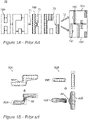
- Figure 1A schematically illustrates the splitting of 2D patterns 75A into simpler patterns 75B and further into elements 75C processed using separate masks 78A, 78B, according to the prior art.
- the multi-patterning schemes split (71) the 2D regions (polygons) into two or more polygons (termed layer decomposition) with stitches 73 and further splits (72) the structures to separated masks for processing (e.g., by double patterning, such as LELE - litho etch litho etch).
- double patterning such as LELE - litho etch litho etch
- Figure 1B schematically illustrates Hot Spots behavior in conjunction with the process window, according to the prior art.
- Illustrations 80A , 80B show schematically two non-limiting examples of hotspots, in a process corner and a process gap, respectively, having a necking hotspot 82 and a bridging hotspot 84 , respectively, as non-limiting examples of the prior art.
- US 7 557 921 discloses proxy targets for monitoring overlay, line end shortening effects and pattern placement errors.
- WO2015/19618 discloses imaging metrology targets and methods, which combine 1D elements designed to provide one-dimensional (ID) imaging metrology signals along at least two measurement directions and 20 elements designed to provide at least one two-dimensional (2D) imaging metrology overlay signal.
- US2003/223630 describes an overlay method for determining the overlay error of a device structure formed during semiconductor processing.
- One aspect of the present invention provides overlay metrology targets comprising at least two periodic structures as recited in claim 1.
- a second aspect of the present invention provides a method as recited in claim 5.
- target design examples presented herein are related to imaging technology, in a non-limiting manner. A similar approach may be used to design scatterometry targets.
- the optical resolution of the overlay (OVL) imaging tool is relatively low and requires using micron level features as resolvable elements of overlay targets.
- non-imaging or non-resolving techniques e.g., scatterometry
- segmentation/dummification e.g., using sub-elements at a smaller scale to fill in target elements of "bigger", micron scale, which usually form a periodic pattern, see Figure 3 ). The proper segmentation brings the overlay target behavior closer to device behavior.
- the orthogonal line segmentation suffers from the Line End Shortening (LES) similar to device, and in case of asymmetric LES due to lithography optics aberration or off-axis illumination this LES could impact the overlay measurement.
- the parallel line segmentation suffers from a kind of PPE (Pattern Placement Error) where the outer lines width in the segmented bar have is different from the width of inner lines.
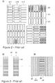
- FIG. 2 is a schematic illustration of periodic structures of an advanced imaging target 90, according to the prior art.
- imaging targets 90 e.g., AIM target - Advanced Imaging Metrology target
- the presented example of AIM target includes periodic structures 91A , 91B , 91C .
- the AIM target usually includes blocks responsible for OVL measurement for both X and Y directions.
- the example on Figure 2 has two blocks for each direction with clockwise symmetry. They are typically designed in an outer, a middle and an inner layer, respectively, which are different layers in the wafer, such as two previously produced layers and a resist layer.
- Periodic structures 91A, 91B, 91C are composed of elements 95 which may be similar or differ from each other in different periodic structures 91A, 91B, 91C according to DR (Design Role) requirements relevant to a specific layer.
- Figure 3 is a high level schematic illustration of elements 95 of periodic structures 91A, 91B, 91C in imaging target 90, according to the prior art.
- Elements 95 are typically segmented bars with sub-elements 96 forming the segmentation of elements 95, and spaces 97 being left empty (as in design 92 ) or being filled with segmented dummification designs 97A (as in design 94 ) with sub-elements 98.
- the segmentation of the bar 95 could be orthogonal 96 or parallel 98. In both prior art cases, sub-elements 96, 98 are symmetric bars.
- Embodiments of the present invention provide efficient and economical methods of converting the "big" target features and using specially designed targets to monitor hot spots like LES together with overlay (or separately therefrom) and decrease the number of required CD-SEM (critical dimension scanning electron microscopy) measurements, which are the prior art way of studying LES and hotspots.
- CD-SEM critical dimension scanning electron microscopy
- Certain embodiments comprise using OVL, tools and OVL algorithms with specially designed target to monitor hot spots and/or the process window.
- OVL OVL
- tools and OVL algorithms with specially designed target to monitor hot spots and/or the process window.
- CD-SEM-like tools for hot spots in-line detection and monitoring which have a very low throughput and a high tool Cost of Ownership (CoO)
- disclosed methods and targets provide effective hot spots monitoring which leads to yield improvement.
- combining the hot spot monitoring and OVL measurement allows to improve the wafer measurement throughput and wafer real estate.
- Metrology imaging targets are provided as a non-limiting example, as well as methods of monitoring process shortcomings.
- Targets comprise periodic structures, at least one of which comprising repeating asymmetric elements along a corresponding segmentation direction of the periodic structure.
- the asymmetry of the elements may be designed in different ways, for example as repeating asymmetric sub-elements along a direction perpendicular to the segmentation direction of the elements.
- the asymmetry of the sub-elements may be designed in different ways, according to the type of monitored process shortcomings, such as various types of hot spots, line edge shortening, process windows parameters and so forth. Results of the measurements may be used to improve the process and/or increase the accuracy of the metrology measurements.
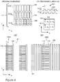
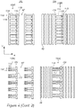
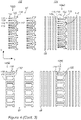
- FIG 4 is a schematic illustration of periodic structures 101 in overlay targets 100 and in parts 109 thereof as well as various exemplary, non-limiting element designs 105A-105E for elements 105 of periodic structures 101 of overlay targets 100, according to some embodiments of the invention.
- Overlay targets 100 may comprise imaging targets 100 and/or scatterometry targets 100, with multiple illustrated parts 109, which may be arranged in various layouts, e.g., in a similar configuration to imaging target 90 of Figure 2 or in other configurations. Any designs of imaging and scatterometry targets may employ periodic structures as disclosed herein, the schematic illustrations are not limiting the embodiments of the invention. Any of the illustrated periodic structures may be part of imaging or scatterometry overlay targets 100.
- Periodic structures 101A, 101B, 101C may be composed of elements 105 which may be similar or differ from each other in different periodic structures 101A, 101B, 101C.
- Periodic structures 101A, 101B, 101C may be designed in different layers and/or with respect to different process steps, for example, periodic structures 101A, 101B, 101C may be at (i) a desired process layer used for overlay measurement, (ii) an anchor same resist layer with segmentation for LES monitoring (e.g., any of 105A-105E or equivalent designs) and (iii) the anchor resist layer (without segmentation).
- any number of different periodic structures 101 may be designed in imaging and/or scatterometry overlay targets 100 (two, three, four, or more periodic structures 101 ) and the design details of elements 105 may be selected according to the purpose of measurement, e.g., LES, hot spots of different types (see above) and additional purposes described below, possible in combination with overlay measurements.
- the target segmentation namely the segmentation of elements 105, may be designed as repeatable pattern(s) of device-like structures. These structures may be way below the optical resolution of the overlay imaging tool and may be designed in a way that the segmented bar (edges or center of mass) moves as a result of LES effect (or other desired type of hot spot for monitoring) - thus indicating the existence and possible extent of LES and/or hotspots.
- Figure 4 schematically exemplifies various such patterns 105A-105E in a non-limiting manner.
- the illustrated examples are applicable both to parts 109 of the OVL target responsible for OVL measurement in the X direction (according to the illustrated directionality), as well as to parts 109 of the OVL target responsible for OVL measurement in the Y direction, which may be e.g., created by rotation the example by 90°.
- Each demonstration includes an example 102 with gaps 97 between respective elements 105A-105E and an example 104 illustrating a bar with parallel segmentation 98 between respective elements 105A-105E.
- Segmented bar 98 may be used as fill-in dummification, as an anchor bar or as any other functional part of the measurement target.
- the parallel bar segmentation was chosen for this example for visualization only, and may be designed differently, based on the required bar functionality and design rules for the specific layer.
- the bar may even be an unsegmented bar or a bar which is segmented asymmetrically.
- Elements 105 may be segmented, repeating and asymmetric along a corresponding measurement direction (denoted in Figure 4 as "Y") of structures 101A, 101B and/or 101C. Repeating asymmetric elements 105 may be internally segmented along a direction (denoted in Figure 4 as "Y") that is perpendicular to the measurement (repeating) direction. Repeating asymmetric elements 105 may comprise repeating sub-elements 110 along the perpendicular direction (Y), the sub-elements being asymmetric in the segmentation direction (X), as illustrated in exemplary designs 105A-105E.
- sub-elements 110 comprise lines which are broken at least once, as illustrated in designs 105A, 105C and 105D by gaps 112.
- Sub-elements 110 may comprise any OPC feature for designs of sub-elements 110 which reduce PPE of one side of sub-elements 110, whereas the opposite side of the sub-elements 110 may be a simple line or include a features designed to monitor the desired hot spots.
- sub-elements 110 may comprise at least two parallel line segments, as illustrated in designs 105B-105E, e.g., by unequal lines 114, 116 in 105B, unequal lines 114, 116 in 105D and lines 110 in 105C, 105E having equal lengths.
- the parallel line segments may be interconnected, as illustrated in design 105D by line segments 114, 116, and in designs 105B and 105E, via interconnecting lines 118.
- sub-elements 110 comprise vertical lines 122 along the perpendicular direction (Y), as illustrated in designs 105C, 105D and 105E.
- lines 110 and/or line segments 114, 116, 119 are interconnected to at least some of vertical lines 122, as exemplified in design 105C
- sub-elements 110 may be interconnected along the perpendicular direction (Y), as illustrated e.g., in designs 105B and 105E.
- sub-elements 110 may be spaced from each other (see spaces 117 ) along the perpendicular direction (Y), as illustrated e.g., in designs 105A, 105C and 105D.
- asymmetric elements 105 may comprise at least one line 120 which is asymmetrically positioned perpendicularly to segmentation direction (X).
- X segmentation direction
- a single vertical line 120 (extending along perpendicular direction Y) is shown, and in design 105E line 118 is positioned similarly.
- the features' dimensions (mainly CD) depend on the design rules for the specific layer and may vary between the minimum allowed by the process (e.g., 7nm for the current most advanced process) up to the maximum allowed by the process (e.g., 300nm in non-limiting examples), and take into account forbidden pitches.
- Certain embodiments comprise scatterometry overlay target having at least one period structure with elements 105 having any of the disclosed design patterns.
- Certain embodiments comprise target design files of targets 100 as well as metrology signals measured from any of targets 100 (the full target design being composed of multiple target elements 105 according to various patterns, see e.g. prior art target pattern 90 ).
- Modifications to the element designs may be made in order to measure Pattern Placement Error (PPE).
- PPE Pattern Placement Error
- Different feature shapes, sizes, pitches, and line to space ratios have different PPEs and may be designed in sub-elements 110 to provide PPE measurements.
- targets 100 may be designed to enable monitoring of any type of hot spots as well as to monitor the process window in any of the processing steps, such as etch and CMP, in addition to the lithography step.
- targets 100 may be used to improve the accuracy of overlay measurement by measuring asymmetric LES, PPE or CMP effect and subtracting from the overlay results.
- the disclosed 2D patterns offer a much wider combination of critical features with respect to the single orientation pattern.
- the measurement of the distance between two opposite line ends (tip-to-tip) or between a line-end perpendicular to a trench (tip-to-trench) may be obtained as function of the process.
- the target designs may be optimized using any lithography simulation software that propagates the target image up to the imaging device of the overlay tool, possibly simulation tools that provide complete target simulation and overlay tool setup optimization.
- the disclosed invention may utilize the standard overlay tool and algorithm without any significant impact on wafer real estate and CoO. Due to high throughput, simplicity of use and short time to results, the disclosed invention may provide a significant increase of hot spots sampling and thus better process monitoring.
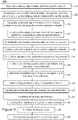
- Figure 5 is a high level flowchart illustrating a method 200, according to some embodiments of the invention.
- the method stages may be carried out with respect to targets 100 described above, which may optionally be designed method 200.
- Method 200 may be at least partially implemented by at least one computer processor (not shown), e.g., in a target design module (not shown).
- Certain embodiments comprise computer program products comprising a computer readable storage medium having computer readable program embodied therewith and configured to carry out the relevant stages of method 200.
- Certain embodiments comprise target design files of respective targets designed by embodiments of method 200.
- Certain embodiments comprise signals measured from targets 100 and/or targets designed by embodiments of method 200.
- Method 200 may include designing targets 100 by lithographic simulations and further comprise optimizing the target designs.
- method 200 comprises designing a metrology imaging target as having at least two periodic structures (stage 210 ) and composing at least one of the periodic structures from repeating asymmetric elements along a corresponding segmentation direction of the periodic structure (stage 220 ).
- method 200 comprises configuring the repeating asymmetric elements to be periodic along a direction perpendicular to the segmentation direction (stage 230 ) and possibly composing the repeating asymmetric elements from repeating asymmetric sub-elements along the perpendicular direction (stage 240 ).
- method 200 comprises configuring the sub-elements to have lines which are broken at least once (stage 242).
- Method 200 may comprise configuring the sub-elements to have at least two parallel line segments (stage 244 ), and may comprise configuring at least some of the parallel line segments to be interconnected (stage 246).
- method 200 comprises introducing vertical lines along the perpendicular direction in at least some of the sub-elements (stage 250 ), and interconnecting at least some of the lines or line segments to at least some of the vertical lines (stage 252 ).
- Method 200 may comprise interconnecting at least some of the sub-elements along the perpendicular direction (stage 260 ) and/or spacing at least some of the sub-elements from each other along the perpendicular direction (stage 270 ).
- Method 200 may comprise positioning vertical line(s) asymmetrically - asymmetrically positioning at least one line which is perpendicular to the segmentation direction (stage 280 ).
- method 200 comprises carrying out designing 210 by at least one computer processor (stage 290 ) and producing the metrology imaging target (stage 292 ) and/or deriving metrology signals from the metrology imaging target (stage 294 ).
- an embodiment is an example or implementation of the invention.
- the various appearances of "one embodiment”, “an embodiment”, “certain embodiments” or “some embodiments” do not necessarily all refer to the same embodiments.
- various features of the invention may be described in the context of a single embodiment, the features may also be provided separately or in any suitable combination.
- the invention may also be implemented in a single embodiment.
- Certain embodiments of the invention may include features from different embodiments disclosed above, and certain embodiments may incorporate elements from other embodiments disclosed above.
- the disclosure of elements of the invention in the context of a specific embodiment is not to be taken as limiting their use in the specific embodiment alone.
- the invention can be carried out or practiced in various ways and that the invention can be implemented in certain embodiments other than the ones outlined in the description above.
Landscapes
- Physics & Mathematics (AREA)
- General Physics & Mathematics (AREA)
- Engineering & Computer Science (AREA)
- Computer Hardware Design (AREA)
- Theoretical Computer Science (AREA)
- Evolutionary Computation (AREA)
- General Engineering & Computer Science (AREA)
- Geometry (AREA)
- Multimedia (AREA)
- Exposure And Positioning Against Photoresist Photosensitive Materials (AREA)
- Preparing Plates And Mask In Photomechanical Process (AREA)
- Image Analysis (AREA)
- Length Measuring Devices By Optical Means (AREA)
- Testing Or Measuring Of Semiconductors Or The Like (AREA)
Applications Claiming Priority (2)
| Application Number | Priority Date | Filing Date | Title |
|---|---|---|---|
| US201662277274P | 2016-01-11 | 2016-01-11 | |
| PCT/US2017/012490 WO2017123464A1 (en) | 2016-01-11 | 2017-01-06 | Hot spot and process window monitoring |
Publications (3)
| Publication Number | Publication Date |
|---|---|
| EP3403142A1 EP3403142A1 (en) | 2018-11-21 |
| EP3403142A4 EP3403142A4 (en) | 2019-09-04 |
| EP3403142B1 true EP3403142B1 (en) | 2022-11-09 |
Family
ID=59312167
Family Applications (1)
| Application Number | Title | Priority Date | Filing Date |
|---|---|---|---|
| EP17738757.8A Active EP3403142B1 (en) | 2016-01-11 | 2017-01-06 | Metrology overlay target and method |
Country Status (8)
| Country | Link |
|---|---|
| US (2) | US10354035B2 (enExample) |
| EP (1) | EP3403142B1 (enExample) |
| JP (2) | JP7117242B2 (enExample) |
| KR (1) | KR102424805B1 (enExample) |
| CN (2) | CN112925177B (enExample) |
| IL (2) | IL259823B (enExample) |
| TW (1) | TWI730031B (enExample) |
| WO (1) | WO2017123464A1 (enExample) |
Families Citing this family (8)
| Publication number | Priority date | Publication date | Assignee | Title |
|---|---|---|---|---|
| US10628544B2 (en) | 2017-09-25 | 2020-04-21 | International Business Machines Corporation | Optimizing integrated circuit designs based on interactions between multiple integration design rules |
| CN109581817B (zh) * | 2017-09-29 | 2021-07-06 | 联华电子股份有限公司 | 半导体装置的形成方法 |
| KR102154959B1 (ko) | 2020-04-29 | 2020-09-10 | 동아에스티 주식회사 | 지속형 glp-1 및 글루카곤 수용체 이중작용제 |
| US11862524B2 (en) | 2021-06-28 | 2024-01-02 | Kla Corporation | Overlay mark design for electron beam overlay |
| US11703767B2 (en) * | 2021-06-28 | 2023-07-18 | Kla Corporation | Overlay mark design for electron beam overlay |
| KR102871169B1 (ko) * | 2021-12-17 | 2025-10-14 | 케이엘에이 코포레이션 | 개선된 타겟 배치 정확성을 위한 오버레이 타겟 설계 |
| US20240053673A1 (en) * | 2022-08-11 | 2024-02-15 | Taiwan Semiconductor Manufacturing Company, Ltd. | Structure and method of signal enhancement for alignment patterns |
| CN116341139B (zh) * | 2023-03-23 | 2025-10-17 | 浙江大学 | 一种提高非对称柱塞泵极限转速的过渡区偏置设计方法 |
Family Cites Families (23)
| Publication number | Priority date | Publication date | Assignee | Title |
|---|---|---|---|---|
| US6128089A (en) * | 1998-07-28 | 2000-10-03 | International Business Machines Corporation | Combined segmented and nonsegmented bar-in-bar targets |
| US7068833B1 (en) * | 2000-08-30 | 2006-06-27 | Kla-Tencor Corporation | Overlay marks, methods of overlay mark design and methods of overlay measurements |
| JP5180419B2 (ja) | 2000-08-30 | 2013-04-10 | ケーエルエー−テンカー・コーポレーション | 重ね合わせマーク、重ね合わせマークの設計方法および重ね合わせ測定の方法 |
| US20030002043A1 (en) | 2001-04-10 | 2003-01-02 | Kla-Tencor Corporation | Periodic patterns and technique to control misalignment |
| US6884552B2 (en) * | 2001-11-09 | 2005-04-26 | Kla-Tencor Technologies Corporation | Focus masking structures, focus patterns and measurements thereof |
| US6772084B2 (en) * | 2002-01-31 | 2004-08-03 | Timbre Technologies, Inc. | Overlay measurements using periodic gratings |
| US7804994B2 (en) | 2002-02-15 | 2010-09-28 | Kla-Tencor Technologies Corporation | Overlay metrology and control method |
| TW200507228A (en) * | 2003-04-08 | 2005-02-16 | Aoti Operating Co Inc | Overlay metrology mark |
| US7112890B2 (en) | 2003-10-30 | 2006-09-26 | Asml Holding N.V. | Tunable alignment geometry |
| JP2006039148A (ja) * | 2004-07-26 | 2006-02-09 | Toshiba Corp | ホトマスク、それを用いたフォーカス測定方法および半導体装置の製造方法 |
| US7655388B2 (en) * | 2005-01-03 | 2010-02-02 | Chartered Semiconductor Manufacturing, Ltd. | Mask and method to pattern chromeless phase lithography contact hole |
| US7557921B1 (en) * | 2005-01-14 | 2009-07-07 | Kla-Tencor Technologies Corporation | Apparatus and methods for optically monitoring the fidelity of patterns produced by photolitographic tools |
| DE102005046973B4 (de) * | 2005-09-30 | 2014-01-30 | Globalfoundries Inc. | Struktur und Verfahren zum gleichzeitigen Bestimmen einer Überlagerungsgenauigkeit und eines Musteranordnungsfehlers |
| US20070111109A1 (en) * | 2005-11-14 | 2007-05-17 | Taiwan Semiconductor Manufacturing Company, Ltd. | Photolithography scattering bar structure and method |
| NL1036856A1 (nl) | 2008-04-24 | 2009-10-27 | Asml Netherlands Bv | Inspection method and apparatus, lithographic apparatus, lithographic processing cell and device manufacturing method. |
| EP2392970A3 (en) | 2010-02-19 | 2017-08-23 | ASML Netherlands BV | Method and apparatus for controlling a lithographic apparatus |
| US20120154773A1 (en) | 2010-12-17 | 2012-06-21 | Carl Zeiss Sms Gmbh | Method and apparatus for correcting errors on a wafer processed by a photolithographic mask |
| NL2010905A (en) * | 2012-06-22 | 2013-12-24 | Asml Netherlands Bv | Method of determining focus, inspection apparatus, patterning device, substrate and device manufacturing method. |
| JP6478974B2 (ja) * | 2013-04-10 | 2019-03-06 | ケーエルエー−テンカー コーポレイション | 標的設計及び製造における誘導自己組織化 |
| US20150043391A1 (en) | 2013-08-08 | 2015-02-12 | Sharp Laboratories Of America, Inc. | Systems and methods for reconfiguration signaling |
| US10001711B2 (en) | 2013-12-17 | 2018-06-19 | Asml Netherlands B.V. | Inspection method, lithographic apparatus, mask and substrate |
| WO2015196168A1 (en) * | 2014-06-21 | 2015-12-23 | Kla-Tencor Corporation | Compound imaging metrology targets |
| WO2016187062A1 (en) * | 2015-05-15 | 2016-11-24 | Kla-Tencor Corporation | System and method for focus determination using focus-sensitive overlay targets |
-
2017
- 2017-01-06 JP JP2018536101A patent/JP7117242B2/ja active Active
- 2017-01-06 WO PCT/US2017/012490 patent/WO2017123464A1/en not_active Ceased
- 2017-01-06 EP EP17738757.8A patent/EP3403142B1/en active Active
- 2017-01-06 US US15/509,728 patent/US10354035B2/en active Active
- 2017-01-06 KR KR1020187023048A patent/KR102424805B1/ko active Active
- 2017-01-06 CN CN202110404661.0A patent/CN112925177B/zh active Active
- 2017-01-06 CN CN201780005930.8A patent/CN108475026B/zh active Active
- 2017-01-11 TW TW106100886A patent/TWI730031B/zh active
-
2018
- 2018-06-05 IL IL259823A patent/IL259823B/en unknown
-
2019
- 2019-06-04 US US16/431,330 patent/US10755016B2/en active Active
-
2021
- 2021-08-11 IL IL285530A patent/IL285530B/en unknown
-
2022
- 2022-08-01 JP JP2022122800A patent/JP7477564B2/ja active Active
Also Published As
| Publication number | Publication date |
|---|---|
| IL285530B (en) | 2022-06-01 |
| TWI730031B (zh) | 2021-06-11 |
| JP2019502959A (ja) | 2019-01-31 |
| CN112925177A (zh) | 2021-06-08 |
| IL259823A (en) | 2018-07-31 |
| US10354035B2 (en) | 2019-07-16 |
| CN108475026B (zh) | 2021-04-23 |
| JP7117242B2 (ja) | 2022-08-12 |
| CN108475026A (zh) | 2018-08-31 |
| EP3403142A1 (en) | 2018-11-21 |
| US20180232478A1 (en) | 2018-08-16 |
| KR102424805B1 (ko) | 2022-07-22 |
| KR20180095717A (ko) | 2018-08-27 |
| TW201732660A (zh) | 2017-09-16 |
| WO2017123464A1 (en) | 2017-07-20 |
| US10755016B2 (en) | 2020-08-25 |
| JP2022153592A (ja) | 2022-10-12 |
| IL259823B (en) | 2021-09-30 |
| US20190286781A1 (en) | 2019-09-19 |
| IL285530A (en) | 2021-09-30 |
| EP3403142A4 (en) | 2019-09-04 |
| CN112925177B (zh) | 2022-09-06 |
| JP7477564B2 (ja) | 2024-05-01 |
Similar Documents
| Publication | Publication Date | Title |
|---|---|---|
| EP3403142B1 (en) | Metrology overlay target and method | |
| US9910348B2 (en) | Method of simultaneous lithography and etch correction flow | |
| KR101301876B1 (ko) | 멀티 패터닝 기술을 위한 셀 레이아웃 | |
| JP5355112B2 (ja) | パターンレイアウト作成方法 | |
| US20110202892A1 (en) | Retarget process modeling method, method of fabricating mask using the retarget process modeling method, computer readable storage medium, and imaging system | |
| Park et al. | An efficient rule-based opc approach using a drc tool for 0.18/spl mu/m asic | |
| US8443309B2 (en) | Multifeature test pattern for optical proximity correction model verification | |
| TWI575308B (zh) | 修正輔助圖案的方法 | |
| Jeong et al. | Assessing chip-level impact of double patterning lithography | |
| US8739077B1 (en) | Methods of modifying a physical design of an electrical circuit used in the manufacture of a semiconductor device | |
| US10748821B2 (en) | Method and system for measuring pattern placement error on a wafer | |
| CN109522618B (zh) | 改善基底反射导致离子注入层光刻缺陷的方法 | |
| Sarma et al. | 3D lithography modeling for ground rule development | |
| Sturtevant et al. | Towards the prediction of pattern collapse hotspots for full-chip layouts | |
| Rittman | Nanometer DFM–the tip of the ice | |
| CN118068657A (zh) | 衡量光刻图形圆整度的方法 | |
| Dave et al. | New methodology to predict pattern collapse for 14nm and beyond | |
| Zheng et al. | Assist feature printability prediction by 3-D resist profile reconstruction | |
| Jessen et al. | 32nm design rule evaluation through virtual patterning | |
| Yu et al. | Fast predictive post-opc contact/via printability metric and validation | |
| Al-Imam et al. | SEM based data extraction for model calibration |
Legal Events
| Date | Code | Title | Description |
|---|---|---|---|
| STAA | Information on the status of an ep patent application or granted ep patent |
Free format text: STATUS: THE INTERNATIONAL PUBLICATION HAS BEEN MADE |
|
| PUAI | Public reference made under article 153(3) epc to a published international application that has entered the european phase |
Free format text: ORIGINAL CODE: 0009012 |
|
| STAA | Information on the status of an ep patent application or granted ep patent |
Free format text: STATUS: REQUEST FOR EXAMINATION WAS MADE |
|
| 17P | Request for examination filed |
Effective date: 20180720 |
|
| AK | Designated contracting states |
Kind code of ref document: A1 Designated state(s): AL AT BE BG CH CY CZ DE DK EE ES FI FR GB GR HR HU IE IS IT LI LT LU LV MC MK MT NL NO PL PT RO RS SE SI SK SM TR |
|
| AX | Request for extension of the european patent |
Extension state: BA ME |
|
| DAV | Request for validation of the european patent (deleted) | ||
| DAX | Request for extension of the european patent (deleted) | ||
| A4 | Supplementary search report drawn up and despatched |
Effective date: 20190806 |
|
| RIC1 | Information provided on ipc code assigned before grant |
Ipc: G03F 1/44 20120101ALI20190731BHEP Ipc: G03F 7/20 20060101AFI20190731BHEP |
|
| GRAP | Despatch of communication of intention to grant a patent |
Free format text: ORIGINAL CODE: EPIDOSNIGR1 |
|
| STAA | Information on the status of an ep patent application or granted ep patent |
Free format text: STATUS: GRANT OF PATENT IS INTENDED |
|
| INTG | Intention to grant announced |
Effective date: 20220525 |
|
| GRAS | Grant fee paid |
Free format text: ORIGINAL CODE: EPIDOSNIGR3 |
|
| GRAA | (expected) grant |
Free format text: ORIGINAL CODE: 0009210 |
|
| STAA | Information on the status of an ep patent application or granted ep patent |
Free format text: STATUS: THE PATENT HAS BEEN GRANTED |
|
| AK | Designated contracting states |
Kind code of ref document: B1 Designated state(s): AL AT BE BG CH CY CZ DE DK EE ES FI FR GB GR HR HU IE IS IT LI LT LU LV MC MK MT NL NO PL PT RO RS SE SI SK SM TR |
|
| REG | Reference to a national code |
Ref country code: GB Ref legal event code: FG4D |
|
| REG | Reference to a national code |
Ref country code: CH Ref legal event code: EP Ref country code: AT Ref legal event code: REF Ref document number: 1530758 Country of ref document: AT Kind code of ref document: T Effective date: 20221115 |
|
| REG | Reference to a national code |
Ref country code: DE Ref legal event code: R096 Ref document number: 602017063531 Country of ref document: DE |
|
| REG | Reference to a national code |
Ref country code: NL Ref legal event code: FP Ref country code: IE Ref legal event code: FG4D |
|
| REG | Reference to a national code |
Ref country code: LT Ref legal event code: MG9D |
|
| REG | Reference to a national code |
Ref country code: AT Ref legal event code: MK05 Ref document number: 1530758 Country of ref document: AT Kind code of ref document: T Effective date: 20221109 |
|
| PG25 | Lapsed in a contracting state [announced via postgrant information from national office to epo] |
Ref country code: SE Free format text: LAPSE BECAUSE OF FAILURE TO SUBMIT A TRANSLATION OF THE DESCRIPTION OR TO PAY THE FEE WITHIN THE PRESCRIBED TIME-LIMIT Effective date: 20221109 Ref country code: PT Free format text: LAPSE BECAUSE OF FAILURE TO SUBMIT A TRANSLATION OF THE DESCRIPTION OR TO PAY THE FEE WITHIN THE PRESCRIBED TIME-LIMIT Effective date: 20230309 Ref country code: NO Free format text: LAPSE BECAUSE OF FAILURE TO SUBMIT A TRANSLATION OF THE DESCRIPTION OR TO PAY THE FEE WITHIN THE PRESCRIBED TIME-LIMIT Effective date: 20230209 Ref country code: LT Free format text: LAPSE BECAUSE OF FAILURE TO SUBMIT A TRANSLATION OF THE DESCRIPTION OR TO PAY THE FEE WITHIN THE PRESCRIBED TIME-LIMIT Effective date: 20221109 Ref country code: FI Free format text: LAPSE BECAUSE OF FAILURE TO SUBMIT A TRANSLATION OF THE DESCRIPTION OR TO PAY THE FEE WITHIN THE PRESCRIBED TIME-LIMIT Effective date: 20221109 Ref country code: ES Free format text: LAPSE BECAUSE OF FAILURE TO SUBMIT A TRANSLATION OF THE DESCRIPTION OR TO PAY THE FEE WITHIN THE PRESCRIBED TIME-LIMIT Effective date: 20221109 Ref country code: AT Free format text: LAPSE BECAUSE OF FAILURE TO SUBMIT A TRANSLATION OF THE DESCRIPTION OR TO PAY THE FEE WITHIN THE PRESCRIBED TIME-LIMIT Effective date: 20221109 |
|
| PG25 | Lapsed in a contracting state [announced via postgrant information from national office to epo] |
Ref country code: RS Free format text: LAPSE BECAUSE OF FAILURE TO SUBMIT A TRANSLATION OF THE DESCRIPTION OR TO PAY THE FEE WITHIN THE PRESCRIBED TIME-LIMIT Effective date: 20221109 Ref country code: PL Free format text: LAPSE BECAUSE OF FAILURE TO SUBMIT A TRANSLATION OF THE DESCRIPTION OR TO PAY THE FEE WITHIN THE PRESCRIBED TIME-LIMIT Effective date: 20221109 Ref country code: LV Free format text: LAPSE BECAUSE OF FAILURE TO SUBMIT A TRANSLATION OF THE DESCRIPTION OR TO PAY THE FEE WITHIN THE PRESCRIBED TIME-LIMIT Effective date: 20221109 Ref country code: IS Free format text: LAPSE BECAUSE OF FAILURE TO SUBMIT A TRANSLATION OF THE DESCRIPTION OR TO PAY THE FEE WITHIN THE PRESCRIBED TIME-LIMIT Effective date: 20230309 Ref country code: HR Free format text: LAPSE BECAUSE OF FAILURE TO SUBMIT A TRANSLATION OF THE DESCRIPTION OR TO PAY THE FEE WITHIN THE PRESCRIBED TIME-LIMIT Effective date: 20221109 Ref country code: GR Free format text: LAPSE BECAUSE OF FAILURE TO SUBMIT A TRANSLATION OF THE DESCRIPTION OR TO PAY THE FEE WITHIN THE PRESCRIBED TIME-LIMIT Effective date: 20230210 |
|
| P01 | Opt-out of the competence of the unified patent court (upc) registered |
Effective date: 20230525 |
|
| PG25 | Lapsed in a contracting state [announced via postgrant information from national office to epo] |
Ref country code: SM Free format text: LAPSE BECAUSE OF FAILURE TO SUBMIT A TRANSLATION OF THE DESCRIPTION OR TO PAY THE FEE WITHIN THE PRESCRIBED TIME-LIMIT Effective date: 20221109 Ref country code: RO Free format text: LAPSE BECAUSE OF FAILURE TO SUBMIT A TRANSLATION OF THE DESCRIPTION OR TO PAY THE FEE WITHIN THE PRESCRIBED TIME-LIMIT Effective date: 20221109 Ref country code: EE Free format text: LAPSE BECAUSE OF FAILURE TO SUBMIT A TRANSLATION OF THE DESCRIPTION OR TO PAY THE FEE WITHIN THE PRESCRIBED TIME-LIMIT Effective date: 20221109 Ref country code: DK Free format text: LAPSE BECAUSE OF FAILURE TO SUBMIT A TRANSLATION OF THE DESCRIPTION OR TO PAY THE FEE WITHIN THE PRESCRIBED TIME-LIMIT Effective date: 20221109 Ref country code: CZ Free format text: LAPSE BECAUSE OF FAILURE TO SUBMIT A TRANSLATION OF THE DESCRIPTION OR TO PAY THE FEE WITHIN THE PRESCRIBED TIME-LIMIT Effective date: 20221109 |
|
| REG | Reference to a national code |
Ref country code: DE Ref legal event code: R097 Ref document number: 602017063531 Country of ref document: DE |
|
| PG25 | Lapsed in a contracting state [announced via postgrant information from national office to epo] |
Ref country code: SK Free format text: LAPSE BECAUSE OF FAILURE TO SUBMIT A TRANSLATION OF THE DESCRIPTION OR TO PAY THE FEE WITHIN THE PRESCRIBED TIME-LIMIT Effective date: 20221109 Ref country code: AL Free format text: LAPSE BECAUSE OF FAILURE TO SUBMIT A TRANSLATION OF THE DESCRIPTION OR TO PAY THE FEE WITHIN THE PRESCRIBED TIME-LIMIT Effective date: 20221109 |
|
| REG | Reference to a national code |
Ref country code: CH Ref legal event code: PL |
|
| PLBE | No opposition filed within time limit |
Free format text: ORIGINAL CODE: 0009261 |
|
| STAA | Information on the status of an ep patent application or granted ep patent |
Free format text: STATUS: NO OPPOSITION FILED WITHIN TIME LIMIT |
|
| PG25 | Lapsed in a contracting state [announced via postgrant information from national office to epo] |
Ref country code: LU Free format text: LAPSE BECAUSE OF NON-PAYMENT OF DUE FEES Effective date: 20230106 |
|
| REG | Reference to a national code |
Ref country code: BE Ref legal event code: MM Effective date: 20230131 |
|
| 26N | No opposition filed |
Effective date: 20230810 |
|
| GBPC | Gb: european patent ceased through non-payment of renewal fee |
Effective date: 20230209 |
|
| PG25 | Lapsed in a contracting state [announced via postgrant information from national office to epo] |
Ref country code: LI Free format text: LAPSE BECAUSE OF NON-PAYMENT OF DUE FEES Effective date: 20230131 Ref country code: CH Free format text: LAPSE BECAUSE OF NON-PAYMENT OF DUE FEES Effective date: 20230131 |
|
| PG25 | Lapsed in a contracting state [announced via postgrant information from national office to epo] |
Ref country code: SI Free format text: LAPSE BECAUSE OF FAILURE TO SUBMIT A TRANSLATION OF THE DESCRIPTION OR TO PAY THE FEE WITHIN THE PRESCRIBED TIME-LIMIT Effective date: 20221109 Ref country code: FR Free format text: LAPSE BECAUSE OF NON-PAYMENT OF DUE FEES Effective date: 20230109 Ref country code: BE Free format text: LAPSE BECAUSE OF NON-PAYMENT OF DUE FEES Effective date: 20230131 |
|
| PG25 | Lapsed in a contracting state [announced via postgrant information from national office to epo] |
Ref country code: GB Free format text: LAPSE BECAUSE OF NON-PAYMENT OF DUE FEES Effective date: 20230209 |
|
| PG25 | Lapsed in a contracting state [announced via postgrant information from national office to epo] |
Ref country code: IE Free format text: LAPSE BECAUSE OF NON-PAYMENT OF DUE FEES Effective date: 20230106 Ref country code: GB Free format text: LAPSE BECAUSE OF NON-PAYMENT OF DUE FEES Effective date: 20230209 |
|
| PG25 | Lapsed in a contracting state [announced via postgrant information from national office to epo] |
Ref country code: IT Free format text: LAPSE BECAUSE OF FAILURE TO SUBMIT A TRANSLATION OF THE DESCRIPTION OR TO PAY THE FEE WITHIN THE PRESCRIBED TIME-LIMIT Effective date: 20221109 |
|
| PG25 | Lapsed in a contracting state [announced via postgrant information from national office to epo] |
Ref country code: MC Free format text: LAPSE BECAUSE OF FAILURE TO SUBMIT A TRANSLATION OF THE DESCRIPTION OR TO PAY THE FEE WITHIN THE PRESCRIBED TIME-LIMIT Effective date: 20221109 |
|
| PG25 | Lapsed in a contracting state [announced via postgrant information from national office to epo] |
Ref country code: MC Free format text: LAPSE BECAUSE OF FAILURE TO SUBMIT A TRANSLATION OF THE DESCRIPTION OR TO PAY THE FEE WITHIN THE PRESCRIBED TIME-LIMIT Effective date: 20221109 |
|
| PG25 | Lapsed in a contracting state [announced via postgrant information from national office to epo] |
Ref country code: BG Free format text: LAPSE BECAUSE OF FAILURE TO SUBMIT A TRANSLATION OF THE DESCRIPTION OR TO PAY THE FEE WITHIN THE PRESCRIBED TIME-LIMIT Effective date: 20221109 |
|
| PG25 | Lapsed in a contracting state [announced via postgrant information from national office to epo] |
Ref country code: BG Free format text: LAPSE BECAUSE OF FAILURE TO SUBMIT A TRANSLATION OF THE DESCRIPTION OR TO PAY THE FEE WITHIN THE PRESCRIBED TIME-LIMIT Effective date: 20221109 |
|
| PGFP | Annual fee paid to national office [announced via postgrant information from national office to epo] |
Ref country code: NL Payment date: 20250127 Year of fee payment: 9 |
|
| PGFP | Annual fee paid to national office [announced via postgrant information from national office to epo] |
Ref country code: DE Payment date: 20250129 Year of fee payment: 9 |
|
| PG25 | Lapsed in a contracting state [announced via postgrant information from national office to epo] |
Ref country code: CY Free format text: LAPSE BECAUSE OF FAILURE TO SUBMIT A TRANSLATION OF THE DESCRIPTION OR TO PAY THE FEE WITHIN THE PRESCRIBED TIME-LIMIT; INVALID AB INITIO Effective date: 20170106 |
|
| PG25 | Lapsed in a contracting state [announced via postgrant information from national office to epo] |
Ref country code: HU Free format text: LAPSE BECAUSE OF FAILURE TO SUBMIT A TRANSLATION OF THE DESCRIPTION OR TO PAY THE FEE WITHIN THE PRESCRIBED TIME-LIMIT; INVALID AB INITIO Effective date: 20170106 |
|
| PG25 | Lapsed in a contracting state [announced via postgrant information from national office to epo] |
Ref country code: TR Free format text: LAPSE BECAUSE OF FAILURE TO SUBMIT A TRANSLATION OF THE DESCRIPTION OR TO PAY THE FEE WITHIN THE PRESCRIBED TIME-LIMIT Effective date: 20221109 |