EP3379643B1 - Mehrschichtiges substrat und radarvorrichtung - Google Patents
Mehrschichtiges substrat und radarvorrichtung Download PDFInfo
- Publication number
- EP3379643B1 EP3379643B1 EP16866102.3A EP16866102A EP3379643B1 EP 3379643 B1 EP3379643 B1 EP 3379643B1 EP 16866102 A EP16866102 A EP 16866102A EP 3379643 B1 EP3379643 B1 EP 3379643B1
- Authority
- EP
- European Patent Office
- Prior art keywords
- ground
- vias
- multilayer substrate
- signal line
- ground layer
- Prior art date
- Legal status (The legal status is an assumption and is not a legal conclusion. Google has not performed a legal analysis and makes no representation as to the accuracy of the status listed.)
- Active
Links
Images






Classifications
-
- H—ELECTRICITY
- H01—ELECTRIC ELEMENTS
- H01P—WAVEGUIDES; RESONATORS, LINES, OR OTHER DEVICES OF THE WAVEGUIDE TYPE
- H01P3/00—Waveguides; Transmission lines of the waveguide type
- H01P3/003—Coplanar lines
- H01P3/006—Conductor backed coplanar waveguides
-
- G—PHYSICS
- G01—MEASURING; TESTING
- G01S—RADIO DIRECTION-FINDING; RADIO NAVIGATION; DETERMINING DISTANCE OR VELOCITY BY USE OF RADIO WAVES; LOCATING OR PRESENCE-DETECTING BY USE OF THE REFLECTION OR RERADIATION OF RADIO WAVES; ANALOGOUS ARRANGEMENTS USING OTHER WAVES
- G01S7/00—Details of systems according to groups G01S13/00, G01S15/00, G01S17/00
- G01S7/02—Details of systems according to groups G01S13/00, G01S15/00, G01S17/00 of systems according to group G01S13/00
- G01S7/03—Details of HF subsystems specially adapted therefor, e.g. common to transmitter and receiver
- G01S7/032—Constructional details for solid-state radar subsystems
-
- H—ELECTRICITY
- H01—ELECTRIC ELEMENTS
- H01P—WAVEGUIDES; RESONATORS, LINES, OR OTHER DEVICES OF THE WAVEGUIDE TYPE
- H01P1/00—Auxiliary devices
- H01P1/20—Frequency-selective devices, e.g. filters
- H01P1/212—Frequency-selective devices, e.g. filters suppressing or attenuating harmonic frequencies
-
- H—ELECTRICITY
- H01—ELECTRIC ELEMENTS
- H01P—WAVEGUIDES; RESONATORS, LINES, OR OTHER DEVICES OF THE WAVEGUIDE TYPE
- H01P3/00—Waveguides; Transmission lines of the waveguide type
- H01P3/003—Coplanar lines
-
- H—ELECTRICITY
- H01—ELECTRIC ELEMENTS
- H01P—WAVEGUIDES; RESONATORS, LINES, OR OTHER DEVICES OF THE WAVEGUIDE TYPE
- H01P3/00—Waveguides; Transmission lines of the waveguide type
- H01P3/02—Waveguides; Transmission lines of the waveguide type with two longitudinal conductors
- H01P3/08—Microstrips; Strip lines
-
- H—ELECTRICITY
- H01—ELECTRIC ELEMENTS
- H01P—WAVEGUIDES; RESONATORS, LINES, OR OTHER DEVICES OF THE WAVEGUIDE TYPE
- H01P3/00—Waveguides; Transmission lines of the waveguide type
- H01P3/02—Waveguides; Transmission lines of the waveguide type with two longitudinal conductors
- H01P3/08—Microstrips; Strip lines
- H01P3/081—Microstriplines
- H01P3/082—Multilayer dielectric
-
- H—ELECTRICITY
- H01—ELECTRIC ELEMENTS
- H01P—WAVEGUIDES; RESONATORS, LINES, OR OTHER DEVICES OF THE WAVEGUIDE TYPE
- H01P5/00—Coupling devices of the waveguide type
- H01P5/02—Coupling devices of the waveguide type with invariable factor of coupling
- H01P5/022—Transitions between lines of the same kind and shape, but with different dimensions
- H01P5/028—Transitions between lines of the same kind and shape, but with different dimensions between strip lines
-
- H—ELECTRICITY
- H05—ELECTRIC TECHNIQUES NOT OTHERWISE PROVIDED FOR
- H05K—PRINTED CIRCUITS; CASINGS OR CONSTRUCTIONAL DETAILS OF ELECTRIC APPARATUS; MANUFACTURE OF ASSEMBLAGES OF ELECTRICAL COMPONENTS
- H05K1/00—Printed circuits
- H05K1/02—Details
- H05K1/0213—Electrical arrangements not otherwise provided for
- H05K1/0216—Reduction of cross-talk, noise or electromagnetic interference
-
- H—ELECTRICITY
- H05—ELECTRIC TECHNIQUES NOT OTHERWISE PROVIDED FOR
- H05K—PRINTED CIRCUITS; CASINGS OR CONSTRUCTIONAL DETAILS OF ELECTRIC APPARATUS; MANUFACTURE OF ASSEMBLAGES OF ELECTRICAL COMPONENTS
- H05K1/00—Printed circuits
- H05K1/02—Details
- H05K1/11—Printed elements for providing electric connections to or between printed circuits
- H05K1/115—Via connections; Lands around holes or via connections
-
- H—ELECTRICITY
- H01—ELECTRIC ELEMENTS
- H01P—WAVEGUIDES; RESONATORS, LINES, OR OTHER DEVICES OF THE WAVEGUIDE TYPE
- H01P5/00—Coupling devices of the waveguide type
- H01P5/02—Coupling devices of the waveguide type with invariable factor of coupling
- H01P5/022—Transitions between lines of the same kind and shape, but with different dimensions
-
- H—ELECTRICITY
- H05—ELECTRIC TECHNIQUES NOT OTHERWISE PROVIDED FOR
- H05K—PRINTED CIRCUITS; CASINGS OR CONSTRUCTIONAL DETAILS OF ELECTRIC APPARATUS; MANUFACTURE OF ASSEMBLAGES OF ELECTRICAL COMPONENTS
- H05K2201/00—Indexing scheme relating to printed circuits covered by H05K1/00
- H05K2201/01—Dielectrics
- H05K2201/0183—Dielectric layers
- H05K2201/0195—Dielectric or adhesive layers comprising a plurality of layers, e.g. in a multilayer structure
Definitions
- the present disclosure relates to a multilayer substrate used for transmitting/receiving a high frequency signal, and a radar device having the multilayer substrate.
- a filter circuit or a matching circuit is formed on the multilayer substrate to suppress harmonic waves.
- Patent Literature 1 discloses that a multilayer substrate having good high frequency characteristics can be formed by exposing an inner conductive layer in a multilayer substrate and bringing an exposed portion of the inner conductive layer into contact with a casing as a system ground.
- Patent Literature 1 Japanese Unexamined Patent Application Publication No. 2005-244110
- Patent Literature 1 to expose the inner conductive layer to the outside, it is necessary to form a concave or stepped portion in the substrate, and a shape of the substrate becomes complicated, and thus it is not preferable in terms of cost.
- JP 2000100994 A is related to a high-frequency package.
- a signal line is composed of a microstrip line structure that comprises a package inner part and a package outer part, a strip line structure that is a hermetically sealed part and an embedded microstrip line structure that is a tapered part which connects them together. Therefore, the tapered part can be prevented from causing characteristic impedance mismatching. Furthermore, the embedded microstrip line structure can be comparatively easily formed, so that a high-frequency package of this constitution can be lessened in manufacturing man-hours and manufacturing costs.
- the distance between the edge of a ground plane and its connecting point connected to a conductor wire near to the edge of the ground plane can be made nearly zero so that a high-frequency package can be prevented from deteriorating in transmission characteristic of high-frequency signal due to circuitry structure of stub.
- a waveguide comprises a waveguide comprises an inner conductor arranged in a first layer, a pair of outer conductors comprising a first outer conductor and a second outer conductor, and a pair of slotted shields comprising a first slotted shield and a second slotted shield.
- the first slotted shield and the second slotted shield are arranged in a second layer with a spacing in between to form a section of a ground shield, wherein the second layer is parallel to the first layer.
- the first slotted shield is connected to the first outer conductor and the second slotted shield is connected to the second outer conductor.
- Sturdivant R. et a. "Transitions and interconnects using coplanar waveguide and other three conductor transmission lines", Bridging the spectrum: 1996 IEEE MTT-S International Microwave Symposium Digest, June 17 - 21, 1996, Moscone Convention Center, San Francisco, California, Piscataway, NJ: IEEE Publ. Order Dep., US, 17 June 1996, pages 235 - 238 vol. 1, XP032372672, DOI: 10.1109/MWSYM.1996.508501, ISBN: 978-0-7803-3246-1 is concerned with multilayer substrates allowing high density packaging of microwave components.
- multilayer boards often require the use of vertical interconnects and transitions to and from various transmission line types.
- a packaging approached tailored for airborne radar is considered along with the interconnect transitions used in the model. This includes the use of 3-wire line. Transitions to/from CBCPW, stripline, 3-wire line and microstrip are described along with modelling and test data. In addition, test data is presented on solderless interconnects using button connectors.
- Two input side ground layers and two output side ground layers may be formed, and three or more intermediate ground layers may be formed.
- a length of an intermediate region signal line portion formed in the intermediate region of the signal line may be set to be an integral multiple of the half wavelength of the harmonic wave.
- a length of an input side region signal line portion formed in the input side region of the signal line may be set on the basis of an impedance of the harmonic wave.
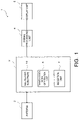
- Fig. 1 is a block diagram of a radar device 1 having a multilayer substrate 10 according to an embodiment outside the subject-matter of the claims .
- the radar device 1 according to the embodiment is mounted in, for example, a vessel as a ship and is used for detecting another ship.
- a transmission wave generated from a transmission signal generated by a transmission/reception device 3 is transmitted from an antenna 2, and a reflection wave in which a transmission wave is reflected by a target and returns is received by the antenna 2 as a reception wave.
- a signal processing unit 4 processes a received signal obtained from the reception wave and generates information (for example, a video signal of an echo image of the target) on the target, and the information is displayed on a display unit 5.
- the multilayer substrate 10 according to the embodiment ,outside the subject-matter of the claims, which disclosure is used for the transmission/reception device 3.
- the multilayer substrate 10 has an input side terminal 17 and an output side terminal 18 (refer to Fig. 2 ).
- the transmission signal generated by the transmission signal generation unit 6 is input to the input side terminal 17 and the transmission signal is output to the antenna 2 side via the output side terminal 18.
- the multilayer substrate 10 in a state in which it is connected to a reception unit 7 of the transmission/reception device 3 by the transmission/reception switching unit, a reception signal obtained from the reception wave received by the antenna 2 is input from the output side terminal 18, and the received signal is output to the reception unit 7 via the input side terminal 17.
- the reception unit 7 outputs the received signal to the signal processing unit 4 after an A/D conversion of the reception signal.
- Fig. 2 is a plan view of the multilayer substrate 10 illustrated in Fig. 1 and is a view illustrating a conductive pattern (first conductive pattern 15) of a top layer (first layer) with diagonal lines.
- Fig. 3 is a schematic view illustrating a cross-sectional shape of the multilayer substrate 10 illustrated in Fig. 2 taken along line III-III and is a view illustrating a state in which a part thereof is omitted.
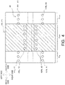
- Fig. 4 is a top view of a conductive pattern (second conductive pattern 25) of a second layer from the top and is a view illustrating a second conductive pattern 25 with diagonal lines.
- Fig. 1 is a plan view of the multilayer substrate 10 illustrated in Fig. 1 and is a view illustrating a conductive pattern (first conductive pattern 15) of a top layer (first layer) with diagonal lines.
- Fig. 3 is a schematic view illustrating a cross-sectional shape of the multilayer substrate 10 illustrated in Fig. 2 taken along line III-
- FIG. 5 is a top view of a conductive pattern (third conductive pattern 30) of a third layer from the top and is a view illustrating a third conductive pattern 30 with diagonal lines.
- Fig. 6 is a top view of a conductive pattern (fourth conductive pattern 35) of a bottom layer (fourth layer) and is a view illustrating a fourth conductive pattern 35 with diagonal lines.
- Fig. 3 to avoid making the drawing complicated, hatching of dielectric layers 11, 12 and 13 is omitted, and a longitudinal dimension of each component with respect to a transverse dimension thereof does not necessarily correspond to an actual dimension.
- an outer shape of the first conductive pattern 15 is illustrated to be superimposed with a broken line.
- a direction indicated by an arrow marked as an input side is referred to as the input side
- a direction indicated by an arrow marked as an output side is referred to as the output side
- a direction indicated by an arrow marked as a right side is referred to as the right side
- a direction indicated by the arrow marked as a left side is referred to as the left side
- a direction indicated by an arrow marked as an upper side is referred to as the upper side or upper direction
- a direction indicated by an arrow marked as a lower side is referred to as the lower side or lower direction.
- the multilayer substrate 10 of the embodiment is a so-called four-layer substrate (a substrate in which four conductive layers are formed) and is a substrate having a particular thickness formed in a rectangular shape in a plan view.
- the multilayer substrate 10 may be divided into three regions in a plan view. Specifically, referring to Figs. 2 , 4 and 6 , the multilayer substrate 10 may be divided into an input side region Z IN on the side in which a signal is input, an output side region Z OUT in which a signal is output, and an intermediate region Z MID sandwiched between the input side region Z IN and the output side region Z OUT .
- the multilayer substrate 10 has three dielectric layers 11, 12 and 13 and four conductive patterns 15, 25, 30 and 35.
- the three dielectric layers 11, 12 and 13 include a first dielectric layer 11, a second dielectric layer 12 and a third dielectric layer 13.
- the first dielectric layer 11 is a dielectric layer provided at the top side among the three dielectric layers, the first conductive pattern 15 is formed on an upper side thereof, and the second conductive pattern 25 is formed on a lower side thereof.
- the second dielectric layer 12 is a dielectric layer formed under the first dielectric layer 11 and is provided in close contact with a lower surface of the second conductive pattern 25.
- the third conductive pattern 30 is provided in close contact with a lower surface of the second dielectric layer 12.
- the third dielectric layer 13 is a dielectric layer formed under the second dielectric layer 12.
- the third conductive pattern 30 is formed on an upper side of the third dielectric layer 13, and the fourth conductive pattern 35 is formed in close contact with a lower side thereof.
- the four conductive patterns 15, 25, 30 and 35 include the first conductive pattern 15, the second conductive pattern 25, the third conductive pattern 30, and the fourth conductive pattern 35.
- the first conductive pattern 15 is formed on a front side (upper side) surface of the first dielectric layer 11. That is, the first conductive pattern 15 is provided as the top conductive pattern and is exposed on the front side (upper side) surface of the multilayer substrate 10.
- the first conductive pattern 15 includes a signal line 16 and a first ground pattern 20 (ground layer).
- the signal line 16 is a conductive pattern which linearly extends from an input side end of the multilayer substrate 10 to an output side end thereof at a center portion of the multilayer substrate 10 in a rightward and leftward direction.
- the signal line 16 includes an input side region signal line portion 16a formed in the input side region Z IN , an intermediate region signal line portion 16b formed in the intermediate region Z MID , and an output side region signal line portion 16c formed in the output side region Z OUT .
- An input side end of the signal line 16 is provided as the input side terminal 17 to which the transmission signal generated by the transmission signal generation unit 6 (refer to Fig. 1 ) is input.
- an output side end of the signal line 16 is provided as the output side terminal 18 through which a signal passing through the signal line 16 is output to the antenna 2 side.
- the first ground pattern 20 is a portion provided as a ground surface in the first conductive pattern. That is, the first ground pattern 20 is formed not to be in contact with the signal line 16.
- the first ground pattern 20 includes an input side region ground layer 21, an intermediate region ground layer 22, and an output side region ground layer 23.
- the input side region ground layer 21 is a portion formed in the input side region Z IN of the first ground pattern 20.
- the input side region ground layer 21 includes an input side region right ground layer 21R formed in a right side of the input side region Z IN , and an input side region left ground layer 21L formed in a left side of the input side region Z IN .
- Each of the input side region right ground layer 21R and the input side region left ground layer 21L is formed in a rectangular shape.
- a distance G IN in the rightward and leftward direction between the input side region right ground layer 21R and the signal line 16 and a distance G IN in the rightward and leftward direction between the input side region left ground layer 21L and the signal line 16 are appropriately set by a designer.
- the intermediate region ground layer 22 is a portion formed in the intermediate region Z MID of the first ground pattern 20.
- the intermediate region ground layer 22 includes an intermediate region right ground layer 22R formed in a right side of the intermediate region Z MID , and an intermediate region left ground layer 22L formed in a left side of the intermediate region Z MID .
- Each of the intermediate region right ground layer 22R and the intermediate region left ground layer 22L is formed in a rectangular shape.
- the intermediate region right ground layer 22R is integrally formed with the input side region right ground layer 21R, and the intermediate region left ground layer 22L is integrally formed with the input side region left ground layer 21L.
- a distance G MID in the rightward and leftward direction between the intermediate region right ground layer 22R and the signal line 16, and a distance G MID in the rightward and leftward direction between the intermediate region left ground layer 22L and the signal line 16 are set shorter than the above-described distances G IN . That is, the intermediate region right ground layer 22R and the intermediate region left ground layer 22L are respectively provided to protrude toward the signal line 16 side than the input side region right ground layer 21R and the input side region left ground layer 21L.
- the output side region ground layer 23 is a portion formed in the output side region Z OUT of the first ground pattern 20.
- the output side region ground layer 23 includes an output side region right ground layer 23R formed in a right side of the output side region Z OUT , and an output side region left ground layer 23L formed in a left side of the output side region Z OUT .
- Each of the output side region right ground layer 23R and the output side region left ground layer 23L is formed in a rectangular shape.
- the output side region right ground layer 23R is integrally formed with the intermediate region right ground layer 22R, and the output side region left ground layer 23L is integrally formed with the intermediate region left ground layer 22L.
- a distance G OUT in the rightward and leftward direction between the output side region right ground layer 23R and the signal line 16 and a distance G OUT in the rightward and leftward direction between the output side region left ground layer 23L and the signal line 16 are set to be equal to the above-described distances G IN .
- the second conductive pattern 25 is formed between the first dielectric layer 11 and the second dielectric layer 12. That is, the second conductive pattern 25 is provided as a second conductive pattern from the top and is embedded in the multilayer substrate 10.
- the second conductive pattern 25 is constituted by a second ground pattern 26 (ground layer or short distance ground layer).
- the second ground pattern 26 is uniformly formed in the intermediate region Z MID and is not formed in the input side region Z IN and the output side region Z OUT . That is, the second ground pattern 26 is provided as an intermediate ground layer.
- the third conductive pattern 30 is provided between the second dielectric layer 12 and the third dielectric layer 13. That is, the third conductive pattern 30 is provided as a third conductive pattern from the top and is embedded in the multilayer substrate 10.
- the third conductive pattern 30 is constituted by a third ground pattern 31 (ground layer).
- the third ground pattern 31 is uniformly formed in the intermediate region Z MID and is not formed in the input side region Z IN and the output side region Z OUT . That is, the third ground pattern 31 is provided as an intermediate ground layer.
- the third ground pattern 31 has the same shape as that of the second ground pattern 26.
- the fourth conductive pattern 35 is formed on a back side (lower side) surface of the third dielectric layer 13. That is, the fourth conductive pattern 35 is provided as a bottom conductive pattern and is exposed at a back side (lower side) surface of the multilayer substrate 10.
- the fourth conductive pattern 35 is constituted by a fourth ground pattern 36 (ground layer or long distance ground layer).
- the fourth ground pattern 36 is uniformly formed over an entire region on the back surface (lower surface) of the third dielectric layer 13.
- the fourth ground pattern 36 includes an input side region ground layer 37 (input side ground layer) formed in the input side region Z IN , an intermediate region ground layer 38 (intermediate ground layer) formed in the intermediate region Z MID , and an output side region ground layer 39 (output side ground layer) formed in the output side region Z OUT .
- the fourth ground pattern 36 is provided as a system ground of the radar device 1.
- a plurality of vias 40 are formed in the multilayer substrate 10.
- Each of the vias 40 vertically passes through the multilayer substrate 10 and electrically connects the ground patterns 20, 26, 31 and 36 of the conductive patterns 15, 25, 30 and 35.
- the plurality of vias 40 include a plurality of input side region vias 41, a plurality of intermediate region vias 42, and a plurality of output side region vias 43.
- the plurality of input side region vias 41 are vias formed in the input side region Z IN .
- the plurality of input side region vias 41 include a plurality of input side region right vias 41R and a plurality of input side region left vias 41L.
- the plurality of (three in the embodiment) input side region right vias 41R are formed on the right side in the input side region Z IN .
- three input side region right vias 41R are arranged in one row from the input side to the output side on the signal line 16 side in the input side region right ground layer 21R.
- the input side region right ground layer 21R of the first ground pattern 20 and the fourth ground pattern 36 are electrically connected by the plurality of input side region right vias 41R.
- the plurality of (three in the embodiment) input side region left vias 41L are formed on the left side in the input side region Z IN .
- three input side region left vias 41L are arranged in one row from the input side to the output side on the signal line 16 side in the input side region left ground layer 21L.
- the input side region left ground layer 21L of the first ground pattern 20 and the fourth ground pattern 36 are electrically connected by the plurality of input side region left vias 41L.
- the plurality of intermediate region vias 42 are vias formed in the intermediate region Z MID .
- the plurality of intermediate region vias 42 include a plurality of intermediate region right vias 42R (first vias) and a plurality of intermediate region left vias 42L (second vias).
- the plurality of (six in the embodiment) intermediate region right vias 42R are formed on the right side in the intermediate region Z MID .
- six intermediate region right vias 42R are arranged in one row from the input side to the output side on the signal line 16 side in the intermediate region right ground layer 22R.
- the intermediate region right ground layer 22R of the first ground pattern 20, the second ground pattern 26, the third ground pattern 31 and the fourth ground pattern 36 are electrically connected by the plurality of intermediate region right vias 42R.
- the plurality of (six in the embodiment) intermediate region left vias 42L are formed on the left side in the intermediate region Z MID .
- six intermediate region left vias 42L are arranged in one row from the input side to the output side on the signal line 16 side in the intermediate region left ground layer 22L.
- the intermediate region left ground layer 22L of the first ground pattern 20, the second ground pattern 26, the third ground pattern 31 and the fourth ground pattern 36 are electrically connected by the plurality of intermediate region left vias 42L.
- the plurality of output side region vias 43 are vias formed in the output side region Z OUT .
- the plurality of output side region vias 43 include a plurality of output side region right vias 43R and a plurality of output side region left vias 43L.
- the plurality of (three in the embodiment) output side region right vias 43R are formed on the right side in the output side region Z OUT .
- three output side region right vias 43R are arranged in one row from the input side to the output side on the signal line 16 side in the output side region right ground layer 23R.
- the output side region right ground layer 23R of the first ground pattern 20 and the fourth ground pattern 36 are electrically connected by the plurality of output side region right vias 43R.
- the plurality of (three in the embodiment) output side region left vias 43L are formed on the left side in the output side region Z OUT .
- three output side region right vias 43R are arranged in one row from the input side to the output side on the signal line 16 side in the output side region left ground layer 23L.
- the output side region left ground layer 23L of the first ground pattern 20 and the fourth ground pattern 36 are electrically connected by the plurality of output side region left vias 43L.
- a filter circuit or a matching circuit is formed on the multilayer substrate to obtain excellent high frequency characteristics.
- the pattern becomes complicated, and a size of the substrate increases.
- Patent Literature 1 discloses that a multilayer substrate having good high frequency characteristics can be formed by exposing an inner conductive layer in the multilayer substrate and bringing an exposed portion of the inner conductive layer into contact with a casing as a system ground.
- a shape of the substrate becomes complicated, it is not preferable in in terms of cost.
- the multilayer substrate 10 is formed so that the ground patterns of a portion (the input side region Z IN and the output side region Z OUT ) thereof in which the signal is input/output has fewer layers than the ground patterns in the intermediate region Z MID .
- the disturbance of an electric field in the portion in which the signal is input/output hardly occurs, a quasi-TEM mode is likely to be formed in that portion. As a result, a transmission characteristic of the signal is improved.
- Fig. 7 is a view illustrating a state in which a simulation graph (illustrated by a broken line in Fig. 7 ) of a transmission characteristic S 21 of a multilayer substrate according to a comparative example is superimposed on a simulation graph (illustrated by a solid line in Fig. 7 ) of a transmission characteristic S 21 of the multilayer substrate 10 according to the embodiment.
- Fig. 8 is a view illustrating a state in which a simulation graph (illustrated by a broken line in Fig. 8 ) of a reflection characteristic S 11 of the multilayer substrate according to the comparative example is superimposed on a simulation graph (illustrated by a solid line in Fig.
- the ground patterns (the second ground pattern and the third ground pattern) of the inner layers are formed over the entire region (the input side region Z IN , the intermediate region Z MID , and the output side region Z OUT ) of the substrate, and other configurations are the same as those of the multilayer substrate 10.
- each value of L1 to L5 is set as follows. Specifically, the value of L1 is set to be a half wavelength of a wavelength ⁇ r of a secondary harmonic wave (18.8 GHz). Also, the value of L2 is set to be an integral multiple of the half wavelength ( ⁇ r /2) of the secondary harmonic wave.
- an impedance of the secondary harmonic wave may be arbitrarily set without affecting an impedance of a fundamental wave (9.4 GHz). Further, a value obtained by adding L4 and L5 is set to be a quarter of the wavelength ⁇ r of the secondary harmonic wave (18.8 GHz).
- L1 is a distance between the intermediate region right via 42R and the intermediate region left via 42L. More specifically, L1 is a distance between an end of the intermediate region right via 42R on the signal line 16 side and an end of the intermediate region left via 42L on the signal line 16 side.
- the dimension of L1 is set to be the half wavelength of the wavelength ⁇ r of the secondary harmonic wave (18.8 GHz).
- the wavelength ⁇ r is a wavelength in consideration of a wavelength shortening effect due to a dielectric constant of the dielectric layer in which the signal line 16 through which the signal is transmitted is formed.
- the wavelength ⁇ r can be calculated, for example, by dividing the wavelength of the secondary harmonic wave in a vacuum by a square root of the dielectric constant of the dielectric layer.
- Fig. 9 is a view illustrating a state in which a graph (illustrated by a square in Fig. 9 ) illustrating a simulation result of the transmission characteristic of the multilayer substrate 10 according to the embodiment ,outside the subject-matter of the claims, and a graph (illustrated by a circle in Fig. 9 ) illustrating a simulation result of the transmission characteristic of the multilayer substrate 100 according to the comparative example are superimposed.
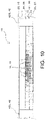
- Fig. 10 is an electric field simulation of the secondary harmonic wave in the multilayer substrate 10 according to the embodiment outside the subject-matter of the claims.
- Fig. 11 is an electric field simulation of the secondary harmonic wave in the multilayer substrate 100 according to the comparative example.
- dimensions of the multilayer substrate 100 according to the comparative example are the same as those of the multilayer substrate 10, except for the fact that the value of L1 is set to be a quarter of the wavelength ⁇ r of the secondary harmonic wave (18.8 GHz).
- the electric field simulations illustrated in Figs. 10 and 11 are electric field simulations when the multilayer substrate is seen from the input side.
- the transmission characteristic of the fundamental wave (9.4 GHz) is substantially the same in both the multilayer substrate 10 and the multilayer substrate 100 according to the comparative example.
- the transmission characteristic of the secondary harmonic wave (18.8 GHz) the multilayer substrate 10 according to the embodiment ,outside the subject-matter of the claims, has superior characteristics (it is difficult to transmit the secondary harmonic wave).
- the inventor of the present disclosure conducted an electric field simulation, and as illustrated in Fig. 11 , according to an electric field simulation result of the multilayer substrate 100 according to the comparative example, it was confirmed that the secondary harmonic wave propagates between the signal line 16 and the conductor of the second layer (the second ground pattern 26). That is, in the multilayer substrate 100 according to the comparative example, the secondary harmonic wave is transmitted to the output side through the signal line.
- the secondary harmonic wave propagates between the conductor of the second layer (the second conductive pattern 25) and the conductor of the fourth layer (the fourth conductive pattern 35), as illustrated in Fig. 10 .
- the second to fourth conductors since the output sides are in an open state, it was confirmed that it is difficult for the secondary harmonic wave to propagate to the output side, as illustrated in Fig. 9 .
- L2 is a length of a portion of the signal line 16 included in the intermediate region Z MID , that is, the intermediate region signal line portion 16b.
- the dimension of L2 is set to be an integral multiple of the half wavelength ( ⁇ r /2) of the secondary harmonic wave.
- Fig. 12 is a view illustrating a state in which the graph (illustrated by a square in Fig. 12 ) illustrating the simulation result of the transmission characteristic of the multilayer substrate 10 according to the embodiment , outside the subject-matter of the claims, and a graph (illustrated by a circle in Fig. 12 ) illustrating a simulation result of a transmission characteristic of a multilayer substrate 101 according to the comparative example are superimposed.
- Fig. 13 is an electric field simulation of the secondary harmonic wave in the multilayer substrate 10 according to the embodiment outside the subject-matter of the claims.
- Fig. 14 is an electric field simulation of the secondary harmonic wave in the multilayer substrate 101 according to the comparative example.
- dimensions of the multilayer substrate 101 according to the comparative example are the same as those of the multilayer substrate 10, except for the fact that the value of L2 is set to be a value obtained by adding a quarter of the wavelength ⁇ r of the secondary harmonic wave (18.8 GHz) to a value obtained by multiplying a half wavelength ( ⁇ r /2) of the secondary harmonic wave by an integer.
- the electric field simulations illustrated in Figs. 13 and 14 are electric field simulations when the multilayer substrate is seen from the input side.
- the transmission characteristic of the fundamental wave (9.4 GHz) is substantially the same in both the multilayer substrate 10 and the multilayer substrate 101 according to the comparative example.
- the transmission characteristic of the secondary harmonic wave (18.8 GHz) the multilayer substrate 10 according to the embodiment has superior characteristics (it is difficult to transmit the secondary harmonic wave).
- the inventor of the present disclosure conducted an electric field simulation, and as illustrated in Fig. 14 , according to an electric field simulation result of the multilayer substrate 101 according to the comparative example, it was confirmed that the secondary harmonic wave propagates between the signal line 16 and the conductor of the second layer (the second conductive pattern 25). That is, in the multilayer substrate 101 according to the comparative example, the secondary harmonic wave is transmitted to the output side through the signal line 16.
- the secondary harmonic wave propagates between the conductor of the second layer (the second conductive pattern 25) and the conductor of the fourth layer (the fourth conductive pattern 35), as illustrated in Fig. 13 .
- the second to fourth conductors since the output sides are in an open state, it was confirmed that it is difficult for the secondary harmonic wave to propagate to the output side, as illustrated in Fig. 12 .
- L3 is a length of a portion of the signal line 16 included in the input side region Z IN , that is, an input side region signal line portion 16a.
- the impedance of the secondary harmonic wave may be arbitrarily set without affecting the impedance of the fundamental wave (9.4 GHz).
- Fig. 15 is a Smith chart illustrating impedances of multilayer substrates 10 having mutually different lengths L3 and is a graph in which an end (illustrated by a circle) on the center side of the chart in each of graphs G1 to G10 illustrated in a straight line indicates the impedance in the fundamental wave and an end (illustrated by an X mark) on the outside of the chart in each of the G1 to G10 indicates the impedance in the secondary harmonic wave.
- a circle mark indicating the impedance in the fundamental wave and an X mark indicating the impedance in the secondary harmonic wave are connected by a broken straight line, but this is merely connecting the circle mark and the X mark with a straight line, and it is not intended that the impedance between the fundamental wave (9.4 GHz) and the secondary harmonic wave (18.8 GHz) is along the straight line.
- Fig. 15 it was confirmed by this simulation that the impedance of the secondary harmonic wave can be adjusted by adjusting the length of L3 without greatly affecting the impedance of the fundamental wave.
- L4 is a distance between a portion of the signal line 16 included in the intermediate region Z MID , that is, the intermediate region signal line portion 16b and the intermediate region right via 42R (or the intermediate region left via 42L) in the rightward and leftward direction.
- L5 is a distance between the second ground pattern 26 and the fourth ground pattern 36.
- a value obtained by adding L4 and L5 is set to be a quarter of the wavelength ⁇ r of the secondary harmonic wave (18.8 GHz).
- Fig. 16 is a graph illustrating the simulation result of the transmission characteristic of the multilayer substrate 10 according to the embodiment , outside the subject-matter of the claims, and is a view illustrating a state in which a graph illustrating the transmission characteristic of the multilayer substrate 10 in which a value of L4 is set to reduce the transmission characteristic of the secondary harmonic wave and a graph illustrating the transmission characteristic of the multilayer substrate 10 in which the value of L4 is set to reduce the transmission characteristic of a tertiary harmonic wave are superimposed.
- the ground layers (two layers of the input side region ground layers 21 and 37 in the embodiment) formed in the input side region Z IN , and the ground layers (two layers of the output side region ground layers 23 and 39 in the embodiment) formed in the output side region Z OUT are formed to have fewer layers than the ground layers (four layers of the intermediate region ground layer 22, the second ground pattern 26, the third ground pattern 31 and the intermediate region ground layer 38 in the embodiment) formed in the intermediate region Z MID .
- the disturbance of the electric field in the portion in which the signal is input/output hardly occurs, and thus the quasi-TEM mode is likely to be formed in that portion. As a result, the transmission characteristic of the signal is improved.
- the multilayer substrate 10 it is possible to provide a multilayer substrate having a simplified configuration and excellent high frequency characteristics.
- the multilayer substrate 10 two ground layers are formed in each of the input side region Z IN and the output side region Z OUT , and three or more (four in the embodiment) ground layers are formed in the intermediate region Z MID . Therefore, as can be understood from the simulation result illustrated in Fig. 7 , good transmission characteristics can be obtained.
- the value of L1 illustrated in Fig. 2 (the distance between the intermediate region right via 42R and the intermediate region left via 42L) is set to be equal to or more than the half wavelength of the secondary harmonic wave and less than the wavelength of the secondary harmonic wave (specifically, in the present embodiment, it is set to be the half wavelength of the secondary harmonic wave). Therefore, as can be seen from the simulation result illustrated in Fig. 9 , the secondary harmonic wave transmitted to the output side can be reduced.
- the value of L2 illustrated in Fig. 2 (the length of the intermediate region signal line portion 16b) is set to be an integral multiple of the half wavelength of the secondary harmonic wave. Therefore, as can be understood from the simulation result illustrated in Fig. 12 , the secondary harmonic wave transmitted to the output side can be reduced.
- the value of L3 (the length of the input side region signal line portion 16a) illustrated in Fig. 2 is set on the basis of the impedance of the secondary harmonic wave to be set.
- the value of L3 the length of the input side region signal line portion 16a
- the impedance of the secondary harmonic wave can be easily adjusted without affecting the impedance of the fundamental wave.
- the values of L4 and L5 are set so that the value obtained by adding L4 and L5 illustrated in Fig. 3 is a quarter of the wavelength of the secondary harmonic wave (or tertiary harmonic wave).
- the secondary harmonic wave (or tertiary harmonic wave) transmitted to the output side can be reduced.
- Fig. 17 is a plan view of a multilayer substrate 10a according to a modified example and is a view illustrating a conductive pattern (first conductive pattern) of a top layer (first layer) with diagonal lines.
- Fig. 18 is a schematic view illustrating a cross-sectional shape of the multilayer substrate 10a illustrated in Fig. 17 taken along line XVIII-XVIII and is a view illustrating a state in which a part thereof is omitted.
- the multilayer substrate 10a according to the modified example has different positions and the number of vias (intermediate region vias) formed in the intermediate region Z MID , as compared with the multilayer substrate 10 according to the above embodiment.
- the hatching of the dielectric layers 11, 12 and 13 is omitted to avoid making the drawing complicated.
- the multilayer substrate 10a In the multilayer substrate 10a according to a modified example, twenty-four intermediate region vias 42a are formed. Twelve of the twenty-four intermediate region vias 42a are formed on the right side in the intermediate region Z MID , and the remaining twelve are formed on the left side in the intermediate region Z MID .
- a plurality of (six in the modified example) intermediate region rightmost vias 44R (first vias) and a plurality of (six in the modified example) intermediate region right vias 45R (third vias) are formed as the intermediate region vias 42a on the right side of the intermediate region Z MID .
- the six intermediate region rightmost vias 44R are arranged in one row from the input side to the output side on the signal line 16 side in the intermediate region right ground layer 22R. Further, referring to Fig. 18 , the intermediate region rightmost vias 44R are provided to extend between the third ground pattern 31 (second long distance ground layer) and the fourth ground pattern 36 (first long distance ground layer) in a vertical direction. Therefore, the third ground pattern 31 and the fourth ground pattern 36 are electrically connected.
- the six intermediate region right vias 45R are arranged in one row from the input side to the output side between the signal line 16 in the intermediate region right ground layer 22R and the intermediate region rightmost vias 44R. Further, referring to Fig. 18 , the intermediate region right vias 45R are provided to extend between the first ground pattern 20 (reference ground layer) and the third ground pattern 31 in a vertical direction. Therefore, the first ground pattern 20, the second ground pattern 26 and the third ground pattern 31 are electrically connected.
- a plurality of (six in the modified example) intermediate region leftmost vias 44L (second vias) and a plurality of (six in the modified example) intermediate region left vias 45L (fourth vias) are formed as the intermediate region vias 42a on the left side of the intermediate region Z MID .
- the six intermediate region leftmost vias 44L are arranged in one row from the input side to the output side on the signal line 16 side in the intermediate region left ground layer 22L. Further, referring to Fig. 18 , the intermediate region leftmost vias 44L are provided to extend between the third ground pattern 31 and the fourth ground pattern 36 in a vertical direction. Therefore, the third ground pattern 31 and the fourth ground pattern 36 are electrically connected.
- the six intermediate region left vias 45L are arranged in one row from the input side to the output side between the signal line 16 in the intermediate region left ground layer 22L and the intermediate region leftmost vias 44L. Further, referring to Fig. 18 , the intermediate region left vias 45L are provided to extend between the first ground pattern 20 and the third ground pattern 31 in a vertical direction. Therefore, the first ground pattern 20, the second ground pattern 26 and the third ground pattern 31 are electrically connected.
- a value of L6 is set to be a half wavelength of the wavelength of the tertiary harmonic wave (28.2 GHz).
- a value of L7 is set to be a half wavelength of the wavelength of the secondary harmonic wave (18.8 GHz).
- L6 and L7 are set to be a half wavelength of the harmonic wave to be cut.
- Fig. 19 is an electric field simulation of the fundamental wave in the multilayer substrate 10a according to the modified example.
- Fig. 20 is an electric field simulation of the secondary harmonic wave in the multilayer substrate 10a according to the modified example.
- Fig. 21 is an electric field simulation of the tertiary harmonic wave in the multilayer substrate 10a according to the modified example.
- the electric field simulations illustrated in Figs. 19 to 21 are electric field simulations when the multilayer substrate 10a is seen from the input side, and in the multilayer substrate 10a schematically illustrated in each drawing, illustration of the via 40 is omitted.
- the electric field is distributed between the signal line 16 and the second ground pattern 26. That is, according to an electric field simulation result illustrated in Fig. 19 , it was confirmed that the fundamental wave is transmitted to the output side via the signal line.
- the electric field is distributed mainly between the third ground pattern 31 and the fourth ground pattern 36. That is, according to the multilayer substrate 10a, it was confirmed that it is difficult for the secondary harmonic wave to be transmitted to the output side.
- the electric field is distributed mainly between the second ground pattern 26 and the third ground pattern 31. That is, according to the multilayer substrate 10a, it was confirmed that it is difficult for the tertiary harmonic wave to be transmitted to the output side.
- the value of L6 (the distance between the intermediate region right via 45R and the intermediate region left via 45L) is set to be equal to or more than the half wavelength of the tertiary harmonic wave and less than the wavelength of the tertiary harmonic wave (specifically, in the present embodiment, it is set to be the half wavelength of the tertiary harmonic wave). Therefore, as can be understood from the electric field simulation result illustrated in Fig. 21 , it is possible to reduce the tertiary harmonic wave transmitted to the output side.
- the value of L7 (the distance between the intermediate region rightmost via 44R and the intermediate region leftmost via 44L) is set to be equal to or more than the half wavelength of the secondary harmonic wave and less than the wavelength of the secondary harmonic wave (specifically, in the present embodiment, it is set to be the half wavelength of the secondary harmonic wave). Therefore, as can be understood from the electric field simulation result illustrated in Fig. 20 , it is possible to reduce the secondary harmonic wave transmitted to the output side.
- transmission of multiple harmonic waves (the secondary harmonic wave and tertiary harmonic wave in the embodiment) desired to reduce the transmission to the output side is easily reduced by appropriately adjusting the values of L6 and L7.
- Fig. 22 is a view schematically illustrating a cross-sectional shape of the multilayer substrate 10b according to the modified example to correspond to Fig. 18 .
- the intermediate region rightmost via 44R and the intermediate region leftmost via 44L are provided to extend between the third ground pattern 31 and the fourth ground pattern 36 in the vertical direction, but the present disclosure is not limited thereto.
- the intermediate region rightmost via 46R and the intermediate region leftmost via 46L may be provided to extend between the first ground pattern 20 and the fourth ground pattern 36 in the vertical direction. Even in this case, it is possible to obtain the same effects as those of the multilayer substrate 10a illustrated in Figs. 17 and 18 .
- the hatching of the dielectric layers 11, 12 and 13 is omitted to avoid making the drawing complicated.
Landscapes
- Engineering & Computer Science (AREA)
- Physics & Mathematics (AREA)
- Microelectronics & Electronic Packaging (AREA)
- Radar, Positioning & Navigation (AREA)
- Remote Sensing (AREA)
- Electromagnetism (AREA)
- Computer Networks & Wireless Communication (AREA)
- General Physics & Mathematics (AREA)
- Production Of Multi-Layered Print Wiring Board (AREA)
- Waveguides (AREA)
- Structure Of Printed Boards (AREA)
Claims (6)
- Mehrschicht-Substrat (10, 10a, 10b), das einen eingangsseitigen Bereich, einen Zwischenbereich und einen ausgangsseitigen Bereich aufweist, und wobei das Mehrschicht-Substrat aufweist:eine Vielzahl dielektrischer Schichten (11, 12, 13);eine Vielzahl von Erdungsschichten (20, 26, 31, 36), die auf beiden Oberflächen von jeder der Vielzahl dielektrischer Schichten vorgesehen sind, und wobei die dielektrischen Schichten über die Erdungsschichten aufeinander gestapelt sind;eine Signalleitung (16), die auf einer Oberfläche einer der Vielzahl von dielektrischen Schichten (11, 12, 13) vorgesehen ist, die auf der Oberseite der Vielzahl dielektrischer Schichten (11, 12,13) vorgesehen ist, und wobei sich die Signalleitung (16) vom eingangsseitigen Bereich über den Zwischenbereich zum ausgangsseitigen Bereich erstreckt, undeine Vielzahl von Durchgangslöchern (40), die die Vielzahl von Erdungsschichten elektrisch verbinden, indem sie durch zumindest eine der Vielzahl dielektrischer Schichten (11, 12, 13) in einer Stapelrichtung der Vielzahl dielektrischer Schichten (11, 12, 13) hindurchgehen, wobeidie Vielzahl von Erdungsschichten aufweist:eine Vielzahl eingangsseitiger Erdungsschichten (21, 37), die in dem eingangsseitigen Bereich vorgesehen sind, wo ein Signal durch die Signalleitung (16) eingespeist wird,eine Vielzahl ausgangsseitiger Erdungsschichten (23, 39), die in dem ausgangsseitigen Bereich vorgesehen sind, wo ein Signal durch die Signalleitung (16) abgegeben wird, undeine Vielzahl dazwischenliegender Erdungsschichten (22, 26, 31, 38), die im Zwischenbereich vorgesehen sind, und wobei die dazwischenliegenden Erdungsschichten zwischen den eingangsseitigen Erdungsschichten (21, 37) und den ausgangsseitigen Erdungsschichten (23, 39) angeordnet sind, unddie eingangsseitigen Erdungsschichten (21, 37), die im eingangsseitigen Bereich vorgesehen sind, weniger Schichten aufweisen als die dazwischenliegende Erdungsschicht (22, 26, 31, 38), die im Zwischenbereich vorgesehen ist, unddie ausgangsseitigen Erdungsschichten (23, 39), die im ausgangsseitigen Bereich vorgesehen sind, weniger Schichten aufweisen als die dazwischenliegende Erdungsschicht (22, 26, 31, 38), die im Zwischenbereich vorgesehen ist,wobei die Vielzahl von Durchgangslöchern (40) eine Vielzahl erster Durchgangslöcher (44R, 46R), eine Vielzahl zweiter Durchgangslöcher (44L, 46L), eine Vielzahl dritter Durchgangslöcher (45R) und eine Vielzahl vierter Durchgangslöcher (45L) aufweist, die in der dazwischenliegenden Erdungsschicht vorgesehen sind,die Vielzahl erster Durchgangslöcher (44R, 46R) in einer Richtung parallel zur Signalleitung (16) auf einer Seite der Signalleitung (16) angeordnet ist,die Vielzahl zweiter Durchgangslöcher (44L, 46L) in einer Richtung parallel zur Signalleitung (16) auf einer anderen Seite der Signalleitung (16) angeordnet ist,die Vielzahl dritter Durchgangslöcher (45R) in einer Richtung parallel zur Signalleitung (16) zwischen der Vielzahl erster Durchgangslöcher (44R, 46R) und der Signalleitung (16) angeordnet ist,die Vielzahl vierter Durchgangslöcher (45L) in einer Richtung parallel zur Signalleitung (16) zwischen der Vielzahl zweiter Durchgangslöcher (44L, 46L) und der Signalleitung (16) angeordnet ist,eine Erdungsschicht (20), die in derselben Schicht wie die Signalleitung (16) angeordnet ist, unter der Vielzahl von Erdungsschichten als Referenz-Erdungsschicht vorgesehen ist,eine Erdungsschicht (36), die unter der Vielzahl von Erdungsschichten in der Stapelrichtung auf einer Seite von der Referenz-Erdungsschicht am weitesten entfernt angeordnet ist, als eine erste Langstrecken-Erdungsschicht vorgesehen ist,eine Erdungsschicht (31), die unter der Vielzahl von Erdungsschichten in der Stapelrichtung der ersten Langstrecken-Erdungsschicht am nächsten liegt, als eine zweite Langstrecken-Erdungsschicht vorgesehen ist,jedes der ersten Durchgangslöcher (44R, 46R) und jedes der zweiten Durchgangslöcher (44L, 46L) sich in der Stapelrichtung erstrecken, um die erste Langstrecken-Erdungsschicht und die zweite Langstrecken-Erdungsschicht elektrisch zu verbinden oder die Referenz-Erdungsschicht und die erste Langstrecken-Erdungsschicht elektrisch zu verbinden, und eine Strecke (L7) zwischen den ersten Durchgangslöchern (44R, 46R) und den zweiten Durchgangslöchern (44L, 46L) so festgelegt ist, dass sie größer oder gleich einer halben Wellenlänge einer sekundären Oberschwingung des über die Signalleitung (16) übertragenen und empfangenen Signals und geringer als eine Wellenlänge der sekundären Oberschwingung ist, undjedes der dritten Durchgangslöcher (45R) und jedes der vierten Durchgangslöcher (45L) sich in der Stapelrichtung erstrecken, um die Referenz-Erdungsschicht und die zweite Langstrecken-Erdungsschicht elektrisch zu verbinden, und die Strecke (L6) zwischen den dritten Durchgangslöchern (45R) und den vierten Durchgangslöchern (45L) so festgelegt ist, dass sie größer oder gleich einer halben Wellenlänge einer tertiären Oberschwingung des über die Signalleitung (16) übertragenen und empfangenen Signals und geringer als eine Wellenlänge der tertiären Oberschwingung ist.
- Mehrschicht-Substrat (10, 10a, 10b) nach Anspruch 1, wobei zwei eingangsseitige Erdungsschichten (21, 37) und zwei ausgangsseitige Erdungsschichten (23, 29) ausgebildet sind und drei oder mehr dazwischenliegende Erdungsschichten (22, 26, 31, 38) ausgebildet sind.
- Mehrschicht-Substrat (10, 10a, 10b) nach Anspruch 1, wobei eine Länge (L2) eines Abschnitts der Signalleitung (16) im Zwischenbereich, der im Zwischenbereich der Signalleitung (16) ausgebildet ist, so festgelegt ist, dass sie ein ganzzahlig Vielfaches der halben Wellenlänge der sekundären Oberschwingung ist.
- Mehrschicht-Substrat (10, 10a, 10b) nach Anspruch 3, wobei eine Länge (L3) eines Abschnitts der Signalleitung (16) im eingangsseitigen Bereich, der im eingangsseitigen Bereich der Signalleitung (16) ausgebildet ist, auf der Basis einer Impedanz der sekundären Oberschwingung festgelegt ist.
- Mehrschicht-Substrat (10, 10a, 10b) nach Anspruch 3, wobei ein Wert, der erhalten wird, indem eine Strecke (L4) von dem Abschnitt der Signalleitung (16) im Zwischenbereich, der im Zwischenbereich der Signalleitung (16) ausgebildet ist, zu den ersten Durchgangslöchern (44R, 46R) oder den zweiten Durchgangslöchern (44L, 46L) und eine Strecke (L5) von der Erdungsschicht der Vielzahl von Erdungsschichten, die der Referenz-Erdungsschicht am nächsten liegt, zur ersten Langstrecken-Erdungsschicht addiert werden, so festgelegt ist, dass er ein Viertel der Wellenlänge der sekundären Oberschwingung ist, die über die Signalleitung (16) übertragen und empfangen wird.
- Radarvorrichtung (1), aufweisend das Mehrschicht-Substrat (10, 10a, 10b) nach einem der Ansprüche 1 bis 5.
Applications Claiming Priority (2)
| Application Number | Priority Date | Filing Date | Title |
|---|---|---|---|
| JP2015227747 | 2015-11-20 | ||
| PCT/JP2016/081544 WO2017086100A1 (ja) | 2015-11-20 | 2016-10-25 | 多層基板及びレーダ装置 |
Publications (3)
| Publication Number | Publication Date |
|---|---|
| EP3379643A1 EP3379643A1 (de) | 2018-09-26 |
| EP3379643A4 EP3379643A4 (de) | 2019-07-31 |
| EP3379643B1 true EP3379643B1 (de) | 2022-10-19 |
Family
ID=58718732
Family Applications (1)
| Application Number | Title | Priority Date | Filing Date |
|---|---|---|---|
| EP16866102.3A Active EP3379643B1 (de) | 2015-11-20 | 2016-10-25 | Mehrschichtiges substrat und radarvorrichtung |
Country Status (5)
| Country | Link |
|---|---|
| US (1) | US10594012B2 (de) |
| EP (1) | EP3379643B1 (de) |
| JP (1) | JP6491353B2 (de) |
| CN (1) | CN108370078B (de) |
| WO (1) | WO2017086100A1 (de) |
Families Citing this family (4)
| Publication number | Priority date | Publication date | Assignee | Title |
|---|---|---|---|---|
| CN107390185A (zh) * | 2017-06-07 | 2017-11-24 | 南京燃犀智能科技有限公司 | 一种雷达收发组件的制造方法 |
| CN115280598B (zh) * | 2020-03-09 | 2026-04-03 | 株式会社村田制作所 | 天线模块和搭载天线模块的通信装置 |
| CN114205995A (zh) * | 2021-12-16 | 2022-03-18 | 锐捷网络股份有限公司 | 一种用于传输高速信号的pcb |
| JP7806614B2 (ja) * | 2022-05-19 | 2026-01-27 | 住友電気工業株式会社 | 光モジュール用パッケージおよび光モジュール |
Family Cites Families (12)
| Publication number | Priority date | Publication date | Assignee | Title |
|---|---|---|---|---|
| JP3810566B2 (ja) * | 1998-09-21 | 2006-08-16 | 株式会社住友金属エレクトロデバイス | 高周波用パッケージ |
| JP3241019B2 (ja) | 1999-03-15 | 2001-12-25 | 日本電気株式会社 | コプレーナ線路 |
| JP3664443B2 (ja) * | 2002-12-05 | 2005-06-29 | 松下電器産業株式会社 | 高周波回路および高周波パッケージ |
| KR20030074582A (ko) | 2003-09-03 | 2003-09-19 | 학교법인 한국정보통신학원 | 초고주파 다층회로 구조 및 제작 방법 |
| DE10350033A1 (de) * | 2003-10-27 | 2005-05-25 | Robert Bosch Gmbh | Bauelement mit Koplanarleitung |
| JP2005244110A (ja) | 2004-02-27 | 2005-09-08 | Toshiba Corp | 多層基板及び高周波回路装置 |
| JP4063841B2 (ja) | 2005-09-09 | 2008-03-19 | シャープ株式会社 | 受信装置、受信システム |
| KR100731544B1 (ko) * | 2006-04-13 | 2007-06-22 | 한국전자통신연구원 | 다층배선 코플래너 웨이브가이드 |
| CN101145547A (zh) * | 2006-09-13 | 2008-03-19 | 中国科学院微电子研究所 | 一种降低微波单片集成电路驻波比的地线布图图形 |
| CN101998763B (zh) * | 2010-09-02 | 2013-01-16 | 华为技术有限公司 | 裸芯片与印制电路板的连接结构及印制电路板、通信设备 |
| US20130154773A1 (en) | 2011-12-15 | 2013-06-20 | Infineon Technologies Ag | Waveguide |
| CN203968484U (zh) * | 2011-12-29 | 2014-11-26 | 株式会社村田制作所 | 高频信号线路及电子设备 |
-
2016
- 2016-10-25 CN CN201680067299.XA patent/CN108370078B/zh active Active
- 2016-10-25 US US15/777,212 patent/US10594012B2/en active Active
- 2016-10-25 JP JP2017551792A patent/JP6491353B2/ja active Active
- 2016-10-25 WO PCT/JP2016/081544 patent/WO2017086100A1/ja not_active Ceased
- 2016-10-25 EP EP16866102.3A patent/EP3379643B1/de active Active
Also Published As
| Publication number | Publication date |
|---|---|
| EP3379643A4 (de) | 2019-07-31 |
| JP6491353B2 (ja) | 2019-03-27 |
| US10594012B2 (en) | 2020-03-17 |
| WO2017086100A1 (ja) | 2017-05-26 |
| JPWO2017086100A1 (ja) | 2018-09-06 |
| US20180331407A1 (en) | 2018-11-15 |
| EP3379643A1 (de) | 2018-09-26 |
| CN108370078B (zh) | 2020-10-27 |
| CN108370078A (zh) | 2018-08-03 |
Similar Documents
| Publication | Publication Date | Title |
|---|---|---|
| EP2979321B1 (de) | Übergang zwischen einer siw und einer wellenleiterschnittstelle | |
| US7884682B2 (en) | Waveguide to microstrip transducer having a ridge waveguide and an impedance matching box | |
| JP4958849B2 (ja) | 差動伝送線路 | |
| CN102593565B (zh) | 电介质波导管的输入输出连接构造 | |
| CN110167261A (zh) | 毫米波有源天线单元及pcb板间互连结构 | |
| US20100182105A1 (en) | Impedance-controlled coplanar waveguide system for the three-dimensional distribution of high-bandwidth signals | |
| CN104205249B (zh) | 层叠型多芯电缆 | |
| EP3444892B1 (de) | Leistungsteiler/-kombinierer | |
| EP3379643B1 (de) | Mehrschichtiges substrat und radarvorrichtung | |
| US10811753B2 (en) | Hollow-waveguide-to-planar-waveguide transition including a coupling conductor having one or more conductors branching therefrom | |
| US12087993B2 (en) | Broadband and low cost printed circuit board based 180° hybrid couplers on a single layer board | |
| US12609432B2 (en) | Waveguide | |
| US20180183146A1 (en) | Circuits and techniques for a via-less beamformer | |
| CN114583427B (zh) | 一种高频信号传输装置、天线系统 | |
| CN218677535U (zh) | 一种无源元件的强耦合带状线结构 | |
| EP3624256B1 (de) | Richtkoppler, wellenleitervorrichtung und diplexer | |
| US12160217B2 (en) | High frequency filter | |
| US20210135329A1 (en) | Implementation of inductive posts in an siw structure and production of a generic filter | |
| US20250253510A1 (en) | Mode conversion device | |
| JP4803869B2 (ja) | 誘電体導波管線路の接続構造 | |
| JP2025140677A (ja) | ハイブリッド回路とそれを備えるバトラーマトリクス | |
| US9941562B2 (en) | Microwave-frequency filtering structures | |
| JPH11317604A (ja) | 同軸フィルタ入出力回路 |
Legal Events
| Date | Code | Title | Description |
|---|---|---|---|
| STAA | Information on the status of an ep patent application or granted ep patent |
Free format text: STATUS: THE INTERNATIONAL PUBLICATION HAS BEEN MADE |
|
| PUAI | Public reference made under article 153(3) epc to a published international application that has entered the european phase |
Free format text: ORIGINAL CODE: 0009012 |
|
| STAA | Information on the status of an ep patent application or granted ep patent |
Free format text: STATUS: REQUEST FOR EXAMINATION WAS MADE |
|
| 17P | Request for examination filed |
Effective date: 20180517 |
|
| AK | Designated contracting states |
Kind code of ref document: A1 Designated state(s): AL AT BE BG CH CY CZ DE DK EE ES FI FR GB GR HR HU IE IS IT LI LT LU LV MC MK MT NL NO PL PT RO RS SE SI SK SM TR |
|
| AX | Request for extension of the european patent |
Extension state: BA ME |
|
| DAV | Request for validation of the european patent (deleted) | ||
| DAX | Request for extension of the european patent (deleted) | ||
| A4 | Supplementary search report drawn up and despatched |
Effective date: 20190701 |
|
| RIC1 | Information provided on ipc code assigned before grant |
Ipc: H01P 3/00 20060101AFI20190625BHEP |
|
| STAA | Information on the status of an ep patent application or granted ep patent |
Free format text: STATUS: EXAMINATION IS IN PROGRESS |
|
| 17Q | First examination report despatched |
Effective date: 20201202 |
|
| RIC1 | Information provided on ipc code assigned before grant |
Ipc: H01P 5/02 20060101ALN20220304BHEP Ipc: H01P 3/00 20060101AFI20220304BHEP |
|
| RIC1 | Information provided on ipc code assigned before grant |
Ipc: H01P 5/02 20060101ALN20220316BHEP Ipc: H01P 3/00 20060101AFI20220316BHEP |
|
| RIC1 | Information provided on ipc code assigned before grant |
Ipc: H01P 5/02 20060101ALN20220329BHEP Ipc: H01P 3/00 20060101AFI20220329BHEP |
|
| GRAP | Despatch of communication of intention to grant a patent |
Free format text: ORIGINAL CODE: EPIDOSNIGR1 |
|
| RIC1 | Information provided on ipc code assigned before grant |
Ipc: H01P 5/02 20060101ALN20220407BHEP Ipc: H01P 3/00 20060101AFI20220407BHEP |
|
| STAA | Information on the status of an ep patent application or granted ep patent |
Free format text: STATUS: GRANT OF PATENT IS INTENDED |
|
| INTG | Intention to grant announced |
Effective date: 20220512 |
|
| GRAS | Grant fee paid |
Free format text: ORIGINAL CODE: EPIDOSNIGR3 |
|
| GRAA | (expected) grant |
Free format text: ORIGINAL CODE: 0009210 |
|
| STAA | Information on the status of an ep patent application or granted ep patent |
Free format text: STATUS: THE PATENT HAS BEEN GRANTED |
|
| AK | Designated contracting states |
Kind code of ref document: B1 Designated state(s): AL AT BE BG CH CY CZ DE DK EE ES FI FR GB GR HR HU IE IS IT LI LT LU LV MC MK MT NL NO PL PT RO RS SE SI SK SM TR |
|
| REG | Reference to a national code |
Ref country code: GB Ref legal event code: FG4D |
|
| REG | Reference to a national code |
Ref country code: CH Ref legal event code: EP |
|
| REG | Reference to a national code |
Ref country code: DE Ref legal event code: R096 Ref document number: 602016075802 Country of ref document: DE |
|
| REG | Reference to a national code |
Ref country code: IE Ref legal event code: FG4D |
|
| REG | Reference to a national code |
Ref country code: AT Ref legal event code: REF Ref document number: 1526140 Country of ref document: AT Kind code of ref document: T Effective date: 20221115 |
|
| REG | Reference to a national code |
Ref country code: LT Ref legal event code: MG9D |
|
| REG | Reference to a national code |
Ref country code: NL Ref legal event code: MP Effective date: 20221019 |
|
| REG | Reference to a national code |
Ref country code: AT Ref legal event code: MK05 Ref document number: 1526140 Country of ref document: AT Kind code of ref document: T Effective date: 20221019 |
|
| PG25 | Lapsed in a contracting state [announced via postgrant information from national office to epo] |
Ref country code: NL Free format text: LAPSE BECAUSE OF FAILURE TO SUBMIT A TRANSLATION OF THE DESCRIPTION OR TO PAY THE FEE WITHIN THE PRESCRIBED TIME-LIMIT Effective date: 20221019 |
|
| PG25 | Lapsed in a contracting state [announced via postgrant information from national office to epo] |
Ref country code: SE Free format text: LAPSE BECAUSE OF FAILURE TO SUBMIT A TRANSLATION OF THE DESCRIPTION OR TO PAY THE FEE WITHIN THE PRESCRIBED TIME-LIMIT Effective date: 20221019 Ref country code: PT Free format text: LAPSE BECAUSE OF FAILURE TO SUBMIT A TRANSLATION OF THE DESCRIPTION OR TO PAY THE FEE WITHIN THE PRESCRIBED TIME-LIMIT Effective date: 20230220 Ref country code: NO Free format text: LAPSE BECAUSE OF FAILURE TO SUBMIT A TRANSLATION OF THE DESCRIPTION OR TO PAY THE FEE WITHIN THE PRESCRIBED TIME-LIMIT Effective date: 20230119 Ref country code: LT Free format text: LAPSE BECAUSE OF FAILURE TO SUBMIT A TRANSLATION OF THE DESCRIPTION OR TO PAY THE FEE WITHIN THE PRESCRIBED TIME-LIMIT Effective date: 20221019 Ref country code: FI Free format text: LAPSE BECAUSE OF FAILURE TO SUBMIT A TRANSLATION OF THE DESCRIPTION OR TO PAY THE FEE WITHIN THE PRESCRIBED TIME-LIMIT Effective date: 20221019 Ref country code: ES Free format text: LAPSE BECAUSE OF FAILURE TO SUBMIT A TRANSLATION OF THE DESCRIPTION OR TO PAY THE FEE WITHIN THE PRESCRIBED TIME-LIMIT Effective date: 20221019 Ref country code: AT Free format text: LAPSE BECAUSE OF FAILURE TO SUBMIT A TRANSLATION OF THE DESCRIPTION OR TO PAY THE FEE WITHIN THE PRESCRIBED TIME-LIMIT Effective date: 20221019 |
|
| PG25 | Lapsed in a contracting state [announced via postgrant information from national office to epo] |
Ref country code: RS Free format text: LAPSE BECAUSE OF FAILURE TO SUBMIT A TRANSLATION OF THE DESCRIPTION OR TO PAY THE FEE WITHIN THE PRESCRIBED TIME-LIMIT Effective date: 20221019 Ref country code: PL Free format text: LAPSE BECAUSE OF FAILURE TO SUBMIT A TRANSLATION OF THE DESCRIPTION OR TO PAY THE FEE WITHIN THE PRESCRIBED TIME-LIMIT Effective date: 20221019 Ref country code: LV Free format text: LAPSE BECAUSE OF FAILURE TO SUBMIT A TRANSLATION OF THE DESCRIPTION OR TO PAY THE FEE WITHIN THE PRESCRIBED TIME-LIMIT Effective date: 20221019 Ref country code: IS Free format text: LAPSE BECAUSE OF FAILURE TO SUBMIT A TRANSLATION OF THE DESCRIPTION OR TO PAY THE FEE WITHIN THE PRESCRIBED TIME-LIMIT Effective date: 20230219 Ref country code: HR Free format text: LAPSE BECAUSE OF FAILURE TO SUBMIT A TRANSLATION OF THE DESCRIPTION OR TO PAY THE FEE WITHIN THE PRESCRIBED TIME-LIMIT Effective date: 20221019 Ref country code: GR Free format text: LAPSE BECAUSE OF FAILURE TO SUBMIT A TRANSLATION OF THE DESCRIPTION OR TO PAY THE FEE WITHIN THE PRESCRIBED TIME-LIMIT Effective date: 20230120 |
|
| REG | Reference to a national code |
Ref country code: CH Ref legal event code: PL |
|
| REG | Reference to a national code |
Ref country code: BE Ref legal event code: MM Effective date: 20221031 |
|
| P01 | Opt-out of the competence of the unified patent court (upc) registered |
Effective date: 20230523 |
|
| PG25 | Lapsed in a contracting state [announced via postgrant information from national office to epo] |
Ref country code: LU Free format text: LAPSE BECAUSE OF NON-PAYMENT OF DUE FEES Effective date: 20221025 |
|
| REG | Reference to a national code |
Ref country code: DE Ref legal event code: R097 Ref document number: 602016075802 Country of ref document: DE |
|
| PG25 | Lapsed in a contracting state [announced via postgrant information from national office to epo] |
Ref country code: SM Free format text: LAPSE BECAUSE OF FAILURE TO SUBMIT A TRANSLATION OF THE DESCRIPTION OR TO PAY THE FEE WITHIN THE PRESCRIBED TIME-LIMIT Effective date: 20221019 Ref country code: RO Free format text: LAPSE BECAUSE OF FAILURE TO SUBMIT A TRANSLATION OF THE DESCRIPTION OR TO PAY THE FEE WITHIN THE PRESCRIBED TIME-LIMIT Effective date: 20221019 Ref country code: MC Free format text: LAPSE BECAUSE OF FAILURE TO SUBMIT A TRANSLATION OF THE DESCRIPTION OR TO PAY THE FEE WITHIN THE PRESCRIBED TIME-LIMIT Effective date: 20221019 Ref country code: LI Free format text: LAPSE BECAUSE OF NON-PAYMENT OF DUE FEES Effective date: 20221031 Ref country code: EE Free format text: LAPSE BECAUSE OF FAILURE TO SUBMIT A TRANSLATION OF THE DESCRIPTION OR TO PAY THE FEE WITHIN THE PRESCRIBED TIME-LIMIT Effective date: 20221019 Ref country code: DK Free format text: LAPSE BECAUSE OF FAILURE TO SUBMIT A TRANSLATION OF THE DESCRIPTION OR TO PAY THE FEE WITHIN THE PRESCRIBED TIME-LIMIT Effective date: 20221019 Ref country code: CZ Free format text: LAPSE BECAUSE OF FAILURE TO SUBMIT A TRANSLATION OF THE DESCRIPTION OR TO PAY THE FEE WITHIN THE PRESCRIBED TIME-LIMIT Effective date: 20221019 Ref country code: CH Free format text: LAPSE BECAUSE OF NON-PAYMENT OF DUE FEES Effective date: 20221031 |
|
| PLBE | No opposition filed within time limit |
Free format text: ORIGINAL CODE: 0009261 |
|
| STAA | Information on the status of an ep patent application or granted ep patent |
Free format text: STATUS: NO OPPOSITION FILED WITHIN TIME LIMIT |
|
| PG25 | Lapsed in a contracting state [announced via postgrant information from national office to epo] |
Ref country code: SK Free format text: LAPSE BECAUSE OF FAILURE TO SUBMIT A TRANSLATION OF THE DESCRIPTION OR TO PAY THE FEE WITHIN THE PRESCRIBED TIME-LIMIT Effective date: 20221019 Ref country code: AL Free format text: LAPSE BECAUSE OF FAILURE TO SUBMIT A TRANSLATION OF THE DESCRIPTION OR TO PAY THE FEE WITHIN THE PRESCRIBED TIME-LIMIT Effective date: 20221019 |
|
| 26N | No opposition filed |
Effective date: 20230720 |
|
| PG25 | Lapsed in a contracting state [announced via postgrant information from national office to epo] |
Ref country code: BE Free format text: LAPSE BECAUSE OF NON-PAYMENT OF DUE FEES Effective date: 20221031 |
|
| PG25 | Lapsed in a contracting state [announced via postgrant information from national office to epo] |
Ref country code: IE Free format text: LAPSE BECAUSE OF NON-PAYMENT OF DUE FEES Effective date: 20221025 |
|
| PG25 | Lapsed in a contracting state [announced via postgrant information from national office to epo] |
Ref country code: SI Free format text: LAPSE BECAUSE OF FAILURE TO SUBMIT A TRANSLATION OF THE DESCRIPTION OR TO PAY THE FEE WITHIN THE PRESCRIBED TIME-LIMIT Effective date: 20221019 |
|
| PG25 | Lapsed in a contracting state [announced via postgrant information from national office to epo] |
Ref country code: HU Free format text: LAPSE BECAUSE OF FAILURE TO SUBMIT A TRANSLATION OF THE DESCRIPTION OR TO PAY THE FEE WITHIN THE PRESCRIBED TIME-LIMIT; INVALID AB INITIO Effective date: 20161025 |
|
| PG25 | Lapsed in a contracting state [announced via postgrant information from national office to epo] |
Ref country code: CY Free format text: LAPSE BECAUSE OF FAILURE TO SUBMIT A TRANSLATION OF THE DESCRIPTION OR TO PAY THE FEE WITHIN THE PRESCRIBED TIME-LIMIT Effective date: 20221019 |
|
| PG25 | Lapsed in a contracting state [announced via postgrant information from national office to epo] |
Ref country code: MK Free format text: LAPSE BECAUSE OF FAILURE TO SUBMIT A TRANSLATION OF THE DESCRIPTION OR TO PAY THE FEE WITHIN THE PRESCRIBED TIME-LIMIT Effective date: 20221019 Ref country code: IT Free format text: LAPSE BECAUSE OF FAILURE TO SUBMIT A TRANSLATION OF THE DESCRIPTION OR TO PAY THE FEE WITHIN THE PRESCRIBED TIME-LIMIT Effective date: 20221019 |
|
| PG25 | Lapsed in a contracting state [announced via postgrant information from national office to epo] |
Ref country code: TR Free format text: LAPSE BECAUSE OF FAILURE TO SUBMIT A TRANSLATION OF THE DESCRIPTION OR TO PAY THE FEE WITHIN THE PRESCRIBED TIME-LIMIT Effective date: 20221019 |
|
| PG25 | Lapsed in a contracting state [announced via postgrant information from national office to epo] |
Ref country code: BG Free format text: LAPSE BECAUSE OF FAILURE TO SUBMIT A TRANSLATION OF THE DESCRIPTION OR TO PAY THE FEE WITHIN THE PRESCRIBED TIME-LIMIT Effective date: 20221019 |
|
| PG25 | Lapsed in a contracting state [announced via postgrant information from national office to epo] |
Ref country code: MT Free format text: LAPSE BECAUSE OF FAILURE TO SUBMIT A TRANSLATION OF THE DESCRIPTION OR TO PAY THE FEE WITHIN THE PRESCRIBED TIME-LIMIT Effective date: 20221019 |
|
| PGFP | Annual fee paid to national office [announced via postgrant information from national office to epo] |
Ref country code: GB Payment date: 20250904 Year of fee payment: 10 |
|
| PGFP | Annual fee paid to national office [announced via postgrant information from national office to epo] |
Ref country code: FR Payment date: 20250908 Year of fee payment: 10 |
|
| PGFP | Annual fee paid to national office [announced via postgrant information from national office to epo] |
Ref country code: DE Payment date: 20250902 Year of fee payment: 10 |