EP3379540B1 - Speichervorrichtung und speicherverfahren - Google Patents
Speichervorrichtung und speicherverfahren Download PDFInfo
- Publication number
- EP3379540B1 EP3379540B1 EP18161136.9A EP18161136A EP3379540B1 EP 3379540 B1 EP3379540 B1 EP 3379540B1 EP 18161136 A EP18161136 A EP 18161136A EP 3379540 B1 EP3379540 B1 EP 3379540B1
- Authority
- EP
- European Patent Office
- Prior art keywords
- data
- status
- read
- voltage
- memory unit
- Prior art date
- Legal status (The legal status is an assumption and is not a legal conclusion. Google has not performed a legal analysis and makes no representation as to the accuracy of the status listed.)
- Active
Links
Images





Classifications
-
- G—PHYSICS
- G11—INFORMATION STORAGE
- G11C—STATIC STORES
- G11C16/00—Erasable programmable read-only memories
- G11C16/02—Erasable programmable read-only memories electrically programmable
- G11C16/04—Erasable programmable read-only memories electrically programmable using variable threshold transistors, e.g. FAMOS
- G11C16/0408—Erasable programmable read-only memories electrically programmable using variable threshold transistors, e.g. FAMOS comprising cells containing floating gate transistors
- G11C16/0441—Erasable programmable read-only memories electrically programmable using variable threshold transistors, e.g. FAMOS comprising cells containing floating gate transistors comprising cells containing multiple floating gate devices, e.g. separate read-and-write FAMOS transistors with connected floating gates
-
- G—PHYSICS
- G06—COMPUTING OR CALCULATING; COUNTING
- G06F—ELECTRIC DIGITAL DATA PROCESSING
- G06F3/00—Input arrangements for transferring data to be processed into a form capable of being handled by the computer; Output arrangements for transferring data from processing unit to output unit, e.g. interface arrangements
- G06F3/06—Digital input from, or digital output to, record carriers, e.g. RAID, emulated record carriers or networked record carriers
- G06F3/0601—Interfaces specially adapted for storage systems
- G06F3/0628—Interfaces specially adapted for storage systems making use of a particular technique
- G06F3/0629—Configuration or reconfiguration of storage systems
- G06F3/0634—Configuration or reconfiguration of storage systems by changing the state or mode of one or more devices
-
- G—PHYSICS
- G06—COMPUTING OR CALCULATING; COUNTING
- G06F—ELECTRIC DIGITAL DATA PROCESSING
- G06F3/00—Input arrangements for transferring data to be processed into a form capable of being handled by the computer; Output arrangements for transferring data from processing unit to output unit, e.g. interface arrangements
- G06F3/06—Digital input from, or digital output to, record carriers, e.g. RAID, emulated record carriers or networked record carriers
- G06F3/0601—Interfaces specially adapted for storage systems
- G06F3/0628—Interfaces specially adapted for storage systems making use of a particular technique
- G06F3/0646—Horizontal data movement in storage systems, i.e. moving data in between storage devices or systems
- G06F3/0652—Erasing, e.g. deleting, data cleaning, moving of data to a wastebasket
-
- G—PHYSICS
- G06—COMPUTING OR CALCULATING; COUNTING
- G06F—ELECTRIC DIGITAL DATA PROCESSING
- G06F3/00—Input arrangements for transferring data to be processed into a form capable of being handled by the computer; Output arrangements for transferring data from processing unit to output unit, e.g. interface arrangements
- G06F3/06—Digital input from, or digital output to, record carriers, e.g. RAID, emulated record carriers or networked record carriers
- G06F3/0601—Interfaces specially adapted for storage systems
- G06F3/0668—Interfaces specially adapted for storage systems adopting a particular infrastructure
- G06F3/0671—In-line storage system
- G06F3/0683—Plurality of storage devices
- G06F3/0688—Non-volatile semiconductor memory arrays
-
- G—PHYSICS
- G11—INFORMATION STORAGE
- G11C—STATIC STORES
- G11C16/00—Erasable programmable read-only memories
- G11C16/02—Erasable programmable read-only memories electrically programmable
- G11C16/06—Auxiliary circuits, e.g. for writing into memory
- G11C16/08—Address circuits; Decoders; Word-line control circuits
-
- G—PHYSICS
- G11—INFORMATION STORAGE
- G11C—STATIC STORES
- G11C16/00—Erasable programmable read-only memories
- G11C16/02—Erasable programmable read-only memories electrically programmable
- G11C16/06—Auxiliary circuits, e.g. for writing into memory
- G11C16/10—Programming or data input circuits
-
- G—PHYSICS
- G11—INFORMATION STORAGE
- G11C—STATIC STORES
- G11C16/00—Erasable programmable read-only memories
- G11C16/02—Erasable programmable read-only memories electrically programmable
- G11C16/06—Auxiliary circuits, e.g. for writing into memory
- G11C16/10—Programming or data input circuits
- G11C16/14—Circuits for erasing electrically, e.g. erase voltage switching circuits
-
- G—PHYSICS
- G11—INFORMATION STORAGE
- G11C—STATIC STORES
- G11C16/00—Erasable programmable read-only memories
- G11C16/02—Erasable programmable read-only memories electrically programmable
- G11C16/06—Auxiliary circuits, e.g. for writing into memory
- G11C16/26—Sensing or reading circuits; Data output circuits
-
- G—PHYSICS
- G11—INFORMATION STORAGE
- G11C—STATIC STORES
- G11C16/00—Erasable programmable read-only memories
- G11C16/02—Erasable programmable read-only memories electrically programmable
- G11C16/06—Auxiliary circuits, e.g. for writing into memory
- G11C16/26—Sensing or reading circuits; Data output circuits
- G11C16/28—Sensing or reading circuits; Data output circuits using differential sensing or reference cells, e.g. dummy cells
-
- G—PHYSICS
- G11—INFORMATION STORAGE
- G11C—STATIC STORES
- G11C16/00—Erasable programmable read-only memories
- G11C16/02—Erasable programmable read-only memories electrically programmable
- G11C16/06—Auxiliary circuits, e.g. for writing into memory
- G11C16/30—Power supply circuits
-
- G—PHYSICS
- G11—INFORMATION STORAGE
- G11C—STATIC STORES
- G11C7/00—Arrangements for writing information into, or reading information out from, a digital store
- G11C7/06—Sense amplifiers; Associated circuits, e.g. timing or triggering circuits
-
- G—PHYSICS
- G11—INFORMATION STORAGE
- G11C—STATIC STORES
- G11C7/00—Arrangements for writing information into, or reading information out from, a digital store
- G11C7/06—Sense amplifiers; Associated circuits, e.g. timing or triggering circuits
- G11C7/062—Differential amplifiers of non-latching type, e.g. comparators, long-tailed pairs
-
- G—PHYSICS
- G11—INFORMATION STORAGE
- G11C—STATIC STORES
- G11C7/00—Arrangements for writing information into, or reading information out from, a digital store
- G11C7/10—Input/output [I/O] data interface arrangements, e.g. I/O data control circuits, I/O data buffers
- G11C7/1051—Data output circuits, e.g. read-out amplifiers, data output buffers, data output registers, data output level conversion circuits
- G11C7/1063—Control signal output circuits, e.g. status or busy flags, feedback command signals
-
- G—PHYSICS
- G11—INFORMATION STORAGE
- G11C—STATIC STORES
- G11C2207/00—Indexing scheme relating to arrangements for writing information into, or reading information out from, a digital store
- G11C2207/06—Sense amplifier related aspects
- G11C2207/063—Current sense amplifiers
-
- G—PHYSICS
- G11—INFORMATION STORAGE
- G11C—STATIC STORES
- G11C7/00—Arrangements for writing information into, or reading information out from, a digital store
- G11C7/10—Input/output [I/O] data interface arrangements, e.g. I/O data control circuits, I/O data buffers
- G11C7/1006—Data managing, e.g. manipulating data before writing or reading out, data bus switches or control circuits therefor
Definitions
- the present invention relates to a storage device and a storage method and, for example, relates to a storage device that stores a status flag and a storage method.
- a complementary read flash memory is known as described in, for example, Japanese Unexamined Patent Application Publication No. 2008-117510 .
- two rewritable nonvolatile memory cells form a pair, and 1-bit information is stored in the one pair of memory cells (which can be also referred to hereinafter as a twin cell).
- the cells that constitute the twin cell can be in either a low threshold voltage state or a high threshold voltage state.
- the low threshold voltage state is a state where a threshold voltage (Vth) of a transistor that forms a cell is lower than a specified reference value.
- the high threshold voltage state is a state where a threshold voltage (Vth) of a transistor that forms a cell is equal to or higher than the specified reference value.
- a value of "0" is stored when a first memory cell of a twin cell is in the high threshold voltage state and a second memory cell of the twin cell is in the low threshold voltage state.
- a value of "1” is stored when the first memory cell is in the low threshold voltage state and the second memory cell is in the high threshold voltage state.
- both the first memory cell and the second memory cell are in the low threshold voltage state, they are in an erased state (which is also called an initialized state). In the case of the erased state, a read result from the twin cell is undefined. Specifically, a read value can be "1" or can be "0", which is not a uniquely defined value.
- US 2009/254696 A1 discloses a semiconductor IC having a nonvolatile memory including twin cells, a selector, and a sense circuit.
- a nonvolatile memory including twin cells, a selector, and a sense circuit.
- the pair of nonvolatile memory cells is set to be in a written state where one cell of the pair is set to one of low and high threshold voltages, and the other is set to the other threshold voltage.
- the memory cells both take the low threshold voltage and are made blank.
- the selector includes switching elements. During the blank-check action, switching elements of the selector are controlled to ON state.
- the first total current of the twin cells forced to flow into the first input terminal of the sense circuit commonly is compared with the reference signal on the second input terminal, whereby whether the twin cells have been written or blank can be detected at a high speed.
- the blank-check time can be shortened.
- US 2016/064095 A1 discloses a semiconductor device including a nonvolatile memory of which the memory size of a data area and the memory size of a code area can be freely changed.
- the semiconductor device includes a nonvolatile memory which can switch between a reference current reading system which performs data read by comparing a current flowing through a first memory cell as a read target and the reference current and a complementary reading system which performs data read by comparing currents flowing through a first memory cell and a second memory cell storing complementary data, as a read target.
- the threshold voltages of the memory cells of the twin cell in the erased state tend to maintain the same relationship with each other as that before erasure.
- a value of "0” is likely to be read.
- the twin cell with the value "1” is erased and then this twin cell is read, a value of "1” is likely to be read. Therefore, when the status flag is stored in the twin cell, there is a possibility that a value before erasure may be read even after erasure is done. Thus, there is a possibility that a false status flag value could be read.
- a storage device includes a data memory unit that is read by a complementary read mode and stores data, and a status memory unit that is read by a reference read mode and stores a status flag.
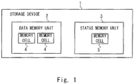
- Fig. 1 is a block diagram showing one example of a storage device 1 according to the overview of the exemplary embodiment.
- the storage device 1 includes a data memory unit (data memory circuit) 2 and a status memory unit (status memory circuit) 3.
- the data memory unit 2 includes a pair of flash memory cells 4.
- the pair of flash memory cells 4 is read by a complementary read mode.
- 1-bit data is stored in this pair of flash memory cells 4.
- the pair of flash memory cells 4 is a twin cell where one flash memory cell 4 is in the low threshold voltage state and the other flash memory cell 4 is in the high threshold voltage state to thereby store 1-bit data.
- the data memory unit 2 is read by the complementary read mode, data is read by comparing a current flowing through one flash memory cell 4 of the twin cell with a current flowing through the other flash memory cell 4 of the twin cell. A current that flows through a memory cell differs according to a threshold voltage of the memory cell.
- the storage device 1 includes one data memory unit 2 in the example shown in Fig. 1
- the storage device 1 may include a plurality of data memory units 2.
- the storage device 1 may include a plurality of pairs of twin cells.
- the status memory unit 3 includes at least one flash memory cell 5.
- the flash memory cell 5 is read by a reference read mode.
- 1-bit information is stored in the one flash memory cell 5.
- a status flag is stored in the flash memory cell 5 of the status memory unit 3.
- the status flag is a flag indicating the status of an arbitrary specified target.
- the reference read mode information is stored by changing the threshold voltage of the flash memory cell 5.
- 1-bit information is stored depending on whether the threshold voltage is equal to or higher than a reference value (i.e., in the high threshold voltage state) or lower than a reference value (i.e., in the low threshold voltage state). For example, a value of "0" is stored when the flash memory cell 5 is in the high threshold voltage state, and a value of "1" is stored when the flash memory cell 5 is in the low threshold voltage state.
- the threshold voltage is changed to a predetermined voltage after erasing is carried out. More specifically, the flash memory cell 5 is set, for example, to the low threshold voltage state by erasing.
- a read result after erasing is a uniquely determined one.
- a read result is a value of "1", for example, in the case where the flash memory cell 5 is set to the low threshold voltage state by erasing.
- the status memory unit 3 is read by the reference read mode, and the status flag is read by comparing a current flowing through the flash memory cell 5 with a reference current. Because the reference current has a constant current value, it is possible to detect the state of the threshold voltage of the flash memory cell 5 by comparing a current flowing through the flash memory cell 5 with the reference current, thereby enabling reading of data. Note that, although the storage device 1 includes one status memory unit 3 in the example shown in Fig. 1 , the storage device 1 may include a plurality of status memory units 3.
- data which is information other than the status flag
- the status flag is stored in the status memory unit 3 that is read by the reference read mode. Therefore, a read result of the status flag after erasing is a uniquely defined one. It is thereby possible in the storage device 1 to store data by the complementary read mode and uniquely define the value of the status flag after erasure.
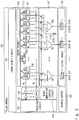
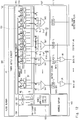
- Fig. 2 is a block diagram showing a configuration example of a flash memory 100 according to a first exemplary embodiment.
- the flash memory 100 corresponds to the storage device 1 shown in Fig. 1 .
- the flash memory 100 includes a power supply circuit 101, a write circuit 102, an address buffer 103, a predecode circuit 104, a decoder 105, a WL driver 106, a sense amplifier circuit 107, a sense amplifier control circuit 108, an output driver 109, and a memory cell array 110.
- the power supply circuit 101 is a circuit that supplies power to be used for writing, erasing and reading.
- the write circuit 102 is a circuit that supplies, to the memory cell array 110, information to be written.
- the address buffer 103 is a circuit that receives an address for access (write access, erase access, and read access) to the memory cell array 110.
- the predecode circuit 104 is a circuit that pre-decodes an address that is output from the address buffer 103.
- the decoder 105 is a circuit that generates a line selection signal for selecting a word line WL to be accessed in accordance with a line predecode signal that is output from the predecode circuit 104.
- the WL driver 106 is a circuit that drives the word line WL in accordance with the line predecode signal.
- the word line WL is a signal line for selecting one arbitrary line in the memory cell array 110.
- a bit line BL is a signal line for outputting a memory cell current of a flash memory cell that is connected with the selected word line WL.
- the sense amplifier circuit 107 is a circuit that senses the current of the bit line BL and outputs a value that is read from the memory cell array 110, and it includes sense amplifiers SA1 and SA2 and a transistor Tr.
- the transistor Tr is a switch that switches the connection state with the bit line BL that is input to the sense amplifier SA1 or SA2. Note that, although one pair of bit lines is selected from a plurality of pairs of bit lines by specifying an address and connected to the sense amplifier in an actual configuration, a bit line selection circuit is shown as a switch in a representative manner in Fig. 2 for the sake of simplifying the figure.
- the sense amplifier control circuit 108 is a control circuit that controls the operation of the sense amplifier circuit 107. Note that the sense amplifier circuit 107 and the sense amplifier control circuit 108 can also be referred to as a determination circuit.
- the output driver 109 is a circuit that latches a value that is output from the sense amplifier circuit 107 by a latch circuit L and then outputs the value as a read result to the outside of the flash memory 100.
- the memory cell array 110 includes a plurality of flash memory cells, which are rewritable nonvolatile memory cells, whose positions are specified by the word line WL and the bit line BL.
- the flash memory cells included in the memory cell array 110 are classified into flash memory cells that form a data memory unit 150 and flash memory cells that form a status memory unit 151.
- the data memory unit 150 corresponds to the data memory unit 2 in Fig. 1 .
- the data memory unit 150 is a memory cell area that includes a pair of memory cells composed of a memory cell M1a and a memory cell M1b.
- the data memory unit 150 stores 1-bit data by the two memory cells: the memory cell M1a and the memory cell M1b. For example, when storing data "0" in the data memory unit 150, the memory cell M1a is set to the high threshold voltage state, and the memory cell M1b is set to the low threshold voltage state, and when storing data "1" in the data memory unit 150, the memory cell M1a is set to the low threshold voltage state, and the memory cell M1b is set to the high threshold voltage state.
- 32 data memory units 150 are placed for each word line WL. Specifically, for each word line WL, 64 memory cells are used as memory cells for the data memory unit 150. Note that those numbers are just an example, and an arbitrary number of data memory units 150 may be placed for each word line WL as a matter of course.
- the 32 data memory units 150 store data D31 to D0, respectively. Each of the data D31 to D0 is 1-bit data.
- bit lines BL i.e., the bit line BL of the memory cell M1a and the bit line BL of the memory cell M1b, of the data memory unit 150 are connected to the sense amplifier SA1.
- the both bit lines BL are connected to the sense amplifier SA1 so as to sense a current difference between the memory cell M1a and the memory cell M1b.
- the bit line BL is connected to the input side of the sense amplifier SA1 through the transistor Tr.
- the sense amplifier SA1 is a circuit that determines the value of data stored in the data memory unit 150 by comparing a current (memory cell current) flowing through one memory cell M1a of the data memory unit 150 and a current (memory cell current) flowing through the other memory cell M1b of the data memory unit 150.
- the sense amplifier SA1 outputs the determined data value as a read result to the output driver 109.
- the data D31 to D0 are output from the output driver 109.
- the status memory unit 151 corresponds to the status memory unit 3 in Fig. 1 .
- the status memory unit 151 is a memory cell area that includes four memory cells M2a, M2b, M2c and M2d.
- the status memory unit 151 stores a status flag and is read by the reference read mode.
- status flag write control may be performed by an arbitrary control circuit. For example, control may be carried out by the write circuit 102 or by a control circuit such as a flash sequencer.
- Each of the memory cells M2a, M2b, M2c and M2d can store 1-bit information.
- the status flag having the same value is stored in each of the memory cells M2a, M2b, M2c and M2d.
- the value of the status flag which is 1-bit information, is stored in all of the memory cells M2a, M2b, M2c and M2d. Therefore, in this exemplary embodiment, substantially the same status flag is stored in each memory cell of the status memory unit 151.
- the status flag that is stored in each memory cell of the status memory unit 151 is a flag indicating a data write status of the data memory unit 150. To be more specific, it is a flag indicating whether the data memory unit 150 is in the state where data is written or in the state where data is erased for each of the 32 data memory units 150 connected to the same word line WL.
- the state where data is written is, in other words, the state where data is stored or data is valid.
- the state where data is erased is, in other words, the state where data is not written or data is invalid.
- each of the memory cells M2a, M2b, M2c and M2d is set to the low threshold voltage state, for example.
- the status flag value "0" is stored in each of the memory cells M2a, M2b, M2c and M2d.
- each of the memory cells M2a, M2b, M2c and M2d is set to the high threshold voltage state, for example.
- the status memory unit 151 is composed of four memory cells in this exemplary embodiment, this is merely an example, and the status memory unit 151 may be composed of one or more memory cells. Further, although one status memory unit 151 is placed as the status flag indicating the write status of the 32 data memory units 150 connected to the same word line WL in this exemplary embodiment, one status memory unit 151 may be placed for N (N is an integer of one or more) number of data memory units 150.
- the status flag that is stored in the status memory unit 151 is read by the reference read mode.
- the bit line BL of the status memory unit 151 is connected to the sense amplifier SA2 where the signal line IL through which the reference current Iref can flow is connected to the input side.
- the bit line BL and the signal line IL are connected to the sense amplifier SA2 so as to sense a current difference between the current of the status memory unit 151 and the reference current.
- the bit lines BL of the memory cells M2a, M2b, M2c and M2d are connected to the sense amplifier SA2 in this exemplary embodiment. Note that, to be more specific, the bit lines BL are connected to the sense amplifier SA2 through the transistor Tr.
- the sense amplifier SA2 is a circuit that determines the value of the status flag that is stored in the status memory unit 151 by comparing the sum of currents (memory cell currents) flowing through the memory cells of the status memory unit 151 with the reference current. Specifically, the sense amplifier SA2 determines the value of the status flag by comparing the sum current of the memory cell current of the memory cell M2a, the memory cell current of the memory cell M2b, the memory cell current of the memory cell M2c and the memory cell current of the memory cell M2d with the reference current.
- the signal line IL through which the reference current Iref to be compared with the memory cell current flows is connected to the input side of the sense amplifier SA2.
- the signal line IL is connected to a constant current source CCS1 that supplies the reference current Iref.
- the sense amplifier SA2 outputs the determined status flag value as a read result to the output driver 109. The status flag is thereby output from the output driver 109.
- the flash memory 100 can output the data D31 to D0 and the status flag in response to a read request from the outside.
- Fig. 3 is a view to explain the sense amplifier SA2 that performs reading by the reference read mode.
- the upper view is a schematic view illustrating the input/output relationship of the sense amplifier SA2
- the lower view is a graph illustrating the temporal transition of a voltage of a signal line that is input to the sense amplifier SA2.
- Fig. 3 illustrates the case where the status memory unit 151 includes only one memory cell for easier understanding of the effect of a difference in the number of memory cells that constitute the status memory unit 151.
- the bit line BL of the memory cell M2a and the signal line IL through which the reference current Iref can flow are connected to the input side of the sense amplifier SA2.
- the bit line BL connected to the memory cell M2a and the signal line IL are pre-charged to reach a specified voltage by control of the sense amplifier control circuit 108.
- discharge start timing t1 discharge of the bit line BL by the memory cell current flowing through the memory cell M2a and discharge of the signal line IL by the reference current Iref are carried out by control of the sense amplifier control circuit 108.
- the sense amplifier SA2 senses a voltage difference between the voltage of the bit line BL and the voltage of the signal line IL and thereby determines the value stored in the memory cell M2a.
- a voltage drop of the bit line BL during discharge depends on the current value flowing through the bit line BL (the current value of the memory cell current), and the voltage drop increases as the current increases. Further, the current value of the memory cell current depends on the threshold voltage of the memory cell. On the other hand, a voltage drop of the signal line IL during discharge depends on the current value of the reference current flowing through the signal line IL. Therefore, the sense amplifier SA2 compares the memory cell current and the reference current by comparing the voltage of the bit line BL and the voltage of the signal line IL after discharge. The sense amplifier SA2 determines the stored value based on a result of the comparison.
- a difference between the voltage of the signal line IL and the voltage of the bit line BL of the memory cell M2a needs to be equal to or more than a sensible voltage difference.
- a difference between the voltage of the signal line IL and the voltage of the bit line BL of the memory cell M2a needs to be equal to or more than a sensible voltage difference at the sense timing t2 as shown in the graph of Fig. 3 (first condition).
- a difference between the voltage of the signal line IL and the voltage of the bit line BL of the memory cell M2a needs to be equal to or more than a sensible voltage difference at the sense timing t2 as shown in the graph of Fig. 3 (second condition). Because it is required to correctly read both of the value of the memory cell M2a where the data write status is in the high threshold voltage state and the value of the memory cell M2a where it is in the low threshold voltage state, both of the first condition and the second condition need to be satisfied.
- Fig. 4 is a view to explain the sense amplifier SA1 that performs reading by the complementary read mode.
- the upper view is a schematic view illustrating the input/output relationship of the sense amplifier SA1
- the lower view is a graph illustrating the temporal transition of a voltage of a signal line that is input to the sense amplifier SA1.
- the bit line BL connected to the memory cell M1a and the bit line BL connected to the memory cell M1b are pre-charged to reach a specified voltage by control of the sense amplifier control circuit 108.
- discharge of the bit line BL by the memory cell current flowing through the memory cell M1a and discharge of the bit line BL by the memory cell current flowing through the memory cell M1b are carried out by control of the sense amplifier control circuit 108.
- the sense amplifier SA1 senses a voltage difference between the both bit lines BL and thereby determines the value stored in the data memory unit 150. In this manner, the sense amplifier SA1 compares the memory cell currents of the memory cells M1a and M1b by comparing the voltages of the both bit lines BL after discharge. The sense amplifier SA1 determines the stored value based on a result of the comparison.
- one memory cell of the memory cells M1a and M1b is in the high threshold voltage state, and the other memory cell is in the low threshold voltage state.
- a difference between the voltage of the bit line BL of the memory cell in the high threshold voltage state and the voltage of the bit line BL of the memory cell in the low threshold voltage state is equal to or more than a sensible voltage difference. Therefore, a difference between the voltage of the bit line BL when the memory cell is in the high threshold voltage state and the voltage of the bit line BL when the memory cell is in the low threshold voltage state can be smaller than that in the reference read mode.
- Fig. 5 is a view to explain the effect of variation in the amount of current in the sense amplifier SA2 that performs reading by the reference read mode.
- the upper view is a schematic view illustrating the input/output relationship of the sense amplifier SA2
- the lower view is a graph illustrating the temporal transition of the voltage of the signal line that is input to the sense amplifier SA2. Note that Fig. 5 , just like Fig. 3 , illustrates the case where the status memory unit 151 includes only one memory cell.
- Fig. 6 is a view to explain the effect of variation in the amount of current in the sense amplifier SA1 that performs reading by the complementary read mode.
- the upper view is a schematic view illustrating the input/output relationship of the sense amplifier SA1
- the lower view is a graph illustrating the temporal transition of the voltage of the signal line that is input to the sense amplifier SA1.
- Variation in memory cell current that depends on temperature conditions and voltage conditions has the same characteristics for the memory cell in the high threshold voltage state and the memory cell in the low threshold voltage state. Specifically, at the sense timing t2, when the voltage of the bit line BL of the memory cell M1a is affected by variation, the voltage of the bit line BL of the memory cell M1b is also affected in the same way.
- the complementary read mode data can be read correctly if a voltage difference between the upper limit of variation in the voltage of the bit line BL of the memory cell in the high threshold voltage state and the upper limit of variation in the voltage of the bit line BL of the memory cell in the low threshold voltage state or a voltage difference between the lower limit of variation in the voltage of the bit line BL of the memory cell in the high threshold voltage state and the lower limit of variation in the voltage of the bit line BL of the memory cell in the low threshold voltage state is equal to or more than a sensible voltage difference.
- a voltage difference between the upper limit of variation in the voltage of the bit line BL of the memory cell in the high threshold voltage state and the upper limit of variation in the voltage of the bit line BL of the memory cell in the low threshold voltage state or a voltage difference between the lower limit of variation in the voltage of the bit line BL of the memory cell in the high threshold voltage state and the lower limit of variation in the voltage of the bit line BL of the memory cell in the low threshold voltage state is equal to or more than a sensible voltage difference
- the complementary read mode it is possible in the complementary read mode to read data correctly even when a difference in threshold voltage between the memory cell that is set to the high threshold voltage state and the memory cell that is set to the low threshold voltage state decreases with an increase in the number of times of writing and the number of times of erasing or with an increase in the data retention period.
- the complementary read mode has better data retention properties than the reference read mode.
- the flash memory 100 includes the data memory unit 150 that is read by the complementary read mode and the status memory unit 151 that is read by the reference read mode. It is thereby possible in the flash memory 100 to uniquely define the value of the status flag after erasure and to store data by the complementary read mode.
- the status memory unit 151 that is read by the reference read mode can achieve equal retention properties to the complementary read mode.
- Equal retention properties to the complementary read mode can be achieved by increasing a difference between the voltage of the bit line BL of the memory cell that constitutes the status memory unit 151 and the voltage of the signal line IL at the sense timing. This can be achieved by connecting a plurality of memory cells having the same value to the bit line BL to obtains a larger memory cell current. Therefore, in the flash memory 100 according to this exemplary embodiment, the status memory unit 151 includes a plurality of flash memory cells in which the status value of the same value is stored.
- Fig. 7 is a view to explain the sense amplifier SA2 in the case of retaining a value in one memory cell M2a by the reference read mode.
- the upper view is a schematic view illustrating the input/output relationship of the sense amplifier SA2
- the lower view is a graph illustrating the temporal transition of the voltage of the signal line that is input to the sense amplifier SA2. Note that the graph takes variation in memory cell current into consideration. In the example shown in Fig. 7 , a voltage difference that is required for sensing is not achieved at the sense timing t2.
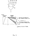
- Fig. 8 is a view to explain the sense amplifier SA2 in the case of retaining the same value in four memory cells M2a to M2d by the reference read mode.
- the upper view is a schematic view illustrating the input/output relationship of the sense amplifier SA2
- the lower view is a graph illustrating the temporal transition of the voltage of the signal line that is input to the sense amplifier SA2. Note that the graph takes variation in memory cell current into consideration.
- the current value of the reference current is set so that the voltage of the signal line IL is a voltage between the voltage of the bit line BL in the high threshold voltage state and the voltage of the bit line BL in the low threshold voltage state.
- both a difference between the lower limit of variation in the voltage of the bit line BL of the memory cells M2a to M2d in the high threshold voltage state and the voltage of the signal line IL and a difference between the upper limit of variation in the voltage of the bit line BL of the memory cells M2a to M2d in the low threshold voltage state and the voltage of the signal line IL can be equal to or more than a voltage difference that is required for sensing. It is thereby possible to read the value correctly.
- the status memory unit 151 that is read by the reference read mode includes a plurality of flash memory cells in this exemplary embodiment, it is possible to improve the retention properties compared with the case where the status memory unit 151 includes only one flash memory.
- this number is merely an example. The number may be determined on the basis of experiment, simulation or the like so as to generate a sufficient voltage difference even with the number of times of writing and the number of times of erasing or after the retention period which are the same as those of the data memory unit 150 in the complementary read mode.
- the status memory unit 151 is read as follows. First, by control of the sense amplifier control circuit 108, the bit lines BL connected respectively to the memory cells M2a to M2d and the signal line IL are pre-charged to reach a specified voltage. After that, at the specified discharge start timing t1, discharge of the bit line BL by the sum current of the currents flowing through the memory cells M2a to M2d and discharge of the signal line IL by the reference current Iref are carried out by control of the sense amplifier control circuit 108.
- the sense amplifier SA2 determines the value stored in the status memory unit 151 by comparing the voltage of the bit line BL and the voltage of the signal line IL after discharge. In other words, the sense amplifier SA2 achieves comparison between the sum current and the reference current by comparing the voltage of the bit line BL and the voltage of the signal line IL after discharge and thereby determines the value.
- the data memory unit 150 and the status memory unit 151 on the same word line WL are preferably erased at the same time. This is because, when the data memory unit 150 is in the erased state, it is guaranteed to obtain the status flag value indicating the erased state as a read result of the status memory unit 151. Further, the flash memory 100 according to this exemplary embodiment is configured so that writing of the status memory unit 151 is carried out separately from writing of the data memory unit 150 on the same word line WL as the status memory unit 151.
- the status memory unit 151 by performing writing to the status memory unit 151 after writing to the data memory unit 150, it is guaranteed that valid data is stored in the data memory unit 150 when a value indicating the state where data is written in the data memory unit 150 is obtained as a read result of the status flag value.
- the data memory unit 150 and the status memory unit 151 on the same word line WL may be erased independently of one another, or writing may be carried out simultaneously with each other. This may be selected as appropriate based on a status which the status flag is used to indicate.
- the flash memory 100 includes the status memory unit 3 that is read by the reference read mode.
- a read result of the status flag after erasing is defined uniquely.
- the status flag is a flag indicating the data write status of the data memory unit 150. Therefore, even after erasing, the flash memory 100 can accurately determine whether the data memory unit 150 is in the state where data is written or in the state where data is erased.
- the status memory unit 151 that is read by the reference read mode includes a plurality of flash memory cells where the status value of the same value is stored. It is thereby possible to improve the retention properties of the status memory unit 151 that is read by the reference read mode.
- the flash memory 100 it is possible to create a flash memory having good retention properties at low costs.
- FIG. 9 is a block diagram showing a configuration example of a flash memory 200 according to the second exemplary embodiment.
- the flash memory 200 is different from the flash memory 100 according to the first exemplary embodiment in that the output driver 109 is replaced by an output driver 111. Note that, in this exemplary embodiment, it is assumed that erasing is carried out simultaneously and also writing is carried out simultaneously in the data memory unit 150 and the status memory unit 151 on the same word line WL.
- the output driver 111 is different from the output driver 109 in that a logical sum circuit OR that carries out the logical OR between a read value from the data memory unit 150 and a read value from the status memory unit 151 is added.
- the output driver 111 can carry out the logical OR between a read value from the data memory unit 150 and a read value from the status memory unit 151 and outputs a result as a read result of the data memory unit 150.
- the logical OR between the data D31 to D0 read by the sense amplifier SA1 and the status flag is carried out.
- data E31 to E0 which is a result of the logical OR operation, is output as a read result of the data memory unit 150.
- the output drive 111 can be also referred to as an output unit (output circuit).
- the data memory unit 150 is read by the complementary read mode, a read value in the erased state is undefined.
- a read value of the status memory unit 151 where erasing is carried out together with erasing of the data memory unit 150 is "1".
- the values of data E31 to E0 that are obtained as a read result after the logical operation are all "1".
- a read value of the status memory unit 151 where writing is carried out together with writing to the data memory unit 150 is "0". Accordingly, when data is written in the data memory unit 150, the values of data E31 to E0 that are obtained as a read result after the logical operation are the same as the values of data D31 to D0.
- Algorithms or software developed for reference read flash memory often determine the status of data based on the assumption that a data read result when a memory cell is in the erased state is fixed to "1".
- the logical OR between a read value from the data memory unit 150 and a status flag is output as a read result of the data memory unit 150.
- the same result as in the flash memory where reading is done only in the reference read mode can be obtained. Therefore, according to this exemplary embodiment, it is possible to use algorithms or software developed for reference read flash memory also for the flash memory 200, which is a flash memory including the complementary read mode.
- FIG. 10 is a block diagram showing a configuration example of a micro controller 10 on which a flash memory 300 according to the third exemplary embodiment is mounted.
- the micro controller 10 can be also referred to as a storage device.
- the micro controller 10 includes a CPU (Central Processing Unit) 400, a RAM (Random Access Memory) 500, a flash memory 300, a voltage monitoring circuit 600, a flash sequencer 700, and a peripheral bus 800.
- the peripheral bus 800 is a bus to which the CPU 400, the voltage monitoring circuit 600 and the flash sequencer 700 are connected.
- the CPU 400 executes processing based on a program (software) and data stored in the flash memory 300 or the RAM 500. Note that, when reading of the flash memory 300 cannot be executed due to during writing or erasing of the flash memory 300 or the like, the CPU 400 can continue processing based on the program by copying the program from the flash memory 300 to the RAM 500 in advance.
- the RAM 500 is a volatile memory in which data or the like to be used by the CPU 400 is stored.
- the flash memory 300 is substantially the same as the flash memory 200 according to the second exemplary embodiment, and it is different in having a memory area to store the interrupt detection flag. The details of the flash memory 300 are described later.
- the voltage monitoring circuit 600 is a circuit that monitors a power supply voltage supplied to the micro controller 10.
- the voltage monitoring circuit 600 can be also referred to as a voltage detection unit (voltage detection circuit).
- the power supply voltage supplied to the micro controller 10 is a voltage of a power supply that is needed for the elements of the micro controller 10 to operate, and it includes a power supply voltage supplied to the flash memory 300, for example.
- the voltage monitoring circuit 600 detects that the power supply voltage becomes equal to or lower than a specified value. When the voltage monitoring circuit 600 detects that the power supply voltage becomes equal to or lower than a specified value, it outputs a voltage decrease detection signal to the flash sequencer 700. In the following description, this specified value is referred to as a voltage decrease detection level.
- the voltage monitoring circuit 600 includes a storage unit (e.g., register) for storing the above-described voltage decrease detection level that is used to determine whether or not to output the voltage decrease detection signal, and the voltage decrease detection level can be changed by rewriting the content of the storage unit. It is thereby possible to flexibly change a threshold for determining the output of the voltage decrease detection signal. To be specific, to make the change, the CPU 400 can rewrite the stored content of the storage unit of the voltage monitoring circuit 600 connected to the peripheral bus 800.
- the voltage monitoring circuit 600 may include a storage unit that stores a set value for determining a voltage monitoring target.
- writing and erasing of the flash memory 300 by the CPU 400 are performed through the flash sequencer 700.
- data reading from the flash memory 300 by the CPU 400 may be performed through the flash sequencer 700 or may be performed directly without through the flash sequencer 700.
- the flash sequencer 700 is a circuit that controls writing, erasing or the like of the flash memory 300.
- the flash sequencer 700 can be also referred to as a control unit (control circuit).
- the flash sequencer 700 includes an address specification register to store address data for specifying an address of the flash memory 300 where writing or erasing is to be carried out. In the address specification register, address data transmitted from the CPU 400 is stored. Further, the flash sequencer 700 includes a command specification register to store a command indicating writing, erasing or the like. In the command specification register, command data transmitted from the CPU 400 is stored.
- the CPU 400 writes command data to the flash sequencer 700 in a predetermined sequence and thereby specifies the details of control to be performed by the flash sequencer 700.
- the flash sequencer 700 performs control corresponding to a series of command data written to the command specification register on the address in the flash memory 300 which is indicated by the address data written to the address specification register.
- Commands of the flash sequencer 700 are described with reference to Fig. 11 as a specific example. As shown in Fig. 11 , a data write command and a data erase command are prepared as the commands to control the flash sequencer 700.
- the CPU 400 In the case of writing data to the flash memory 300, the CPU 400 writes address data to the address specification register through the peripheral bus 800 and thereby specifies the address in the flash memory 300 to which data is to be written. Then, the CPU 400 writes command data indicating write commands sequentially to the command specification register. To be more specific, when writing 4-byte data to the flash memory 300, the CPU 400 writes the command data H'E8, H'02, 4-byte data (2-byte data ⁇ 2) and H'D0 sequentially to the command specification register as shown in Fig. 11 . Further, when writing 16-byte data to the flash memory 300, the CPU 400 writes the command data H'E8, H'08, 16-byte data (2-byte data ⁇ 8) and H'DO sequentially to the command specification register as shown in Fig. 11 . Note that "H'" means that the following numerical value is in hexadecimal notation.
- the flash sequencer 700 writes the data written in the command specification register to the address in the flash memory 300 which is indicated by the address data written in the address specification register. Specifically, when H'02 is written in the second writing, the flash sequencer 700 writes 4-byte data written in the third to fourth writing to the 4-byte area starting from the address specified by the address data. On the other hand, when H'08 is written in the second writing, the flash sequencer 700 writes 16-byte data written in the third to tenth writing to the 16-byte area starting from the address specified by the address data.
- the CPU 400 In the case of erasing data in the flash memory 300, the CPU 400 writes address data to the address specification register through the peripheral bus 800 and thereby specifies the address of a block in the flash memory 300 from which data is to be erased. Then, the CPU 400 writes command data indicating data erase commands sequentially to the command specification register. To be more specific, the CPU 400 writes the command data H'20 and H'DO sequentially to the command specification register. In response thereto, the flash sequencer 700 erases the data of the block in the address in the flash memory 300 which is indicated by the address data written in the address specification register.
- Fig. 12 is a block diagram showing a configuration example of the flash memory 300 according to the third exemplary embodiment.
- the flash memory 300 is different from the flash memory 200 according to the second exemplary embodiment in that the memory cell array 110 includes an interrupt detection memory unit (interrupt detection memory circuit) 152.
- interrupt detection memory circuit interrupt detection memory circuit
- the configurations and operations of the data memory unit 150 and the status memory unit 151 are the same as those of the flash memory 200 according to the second exemplary embodiment.
- the configurations and operations different from those in the second exemplary embodiment are described hereinbelow.
- interrupt detection memory unit 152 is erased simultaneously with the data memory unit 150 and the status memory unit 151 on the same word line WL as an example. It is also assumed that the interrupt detection memory unit 152 can execute writing at different timing from the data memory unit 150 and the status memory unit 151 on the same word line WL.
- the flash memory cells included in the memory cell array 110 are classified into flash memory cells that form the data memory unit 150, flash memory cells that form the status memory unit 151, and flash memory cells that form the interrupt detection memory unit 152.
- the interrupt detection memory unit 152 is a memory cell area that includes four memory cells M3a, M3b, M3c and M3d. Although the interrupt detection memory unit 152 is different from the status memory unit 151 in that it stores the interrupt detection flag, it has the same configuration as the status memory unit 151. Thus, the interrupt detection memory unit 152 includes flash memory cells that are read by the reference read mode. By those flash memory cells, the interrupt detection flag indicating whether there is an interruption of writing or not is stored.
- each of the memory cells M3a, M3b, M3c and M3d can store 1-bit information.
- the interrupt detection flag having the same value is stored in each of the memory cells M3a, M3b, M3c and M3d, just like the status memory unit 151.
- the value of the interrupt detection flag, which is 1-bit information is stored in all of the memory cells M3a, M3b, M3c and M3d. Therefore, in this exemplary embodiment, the interrupt detection memory unit 152 stores substantially 1-bit information.
- the interrupt detection flag that is stored in the interrupt detection memory unit 152 is a flag indicating that writing to the data memory unit 150 has been interrupted. To be more specific, it is a flag indicating whether or not an interruption of writing occurs during writing in the 32 data memory units 150 connected to the same word line WL.
- each of the memory cells M3a, M3b, M3c and M3d is set to the low threshold voltage state, for example.
- "0" is stored as the interrupt detection flag value in each of the memory cells M3a, M3b, M3c and M3d.
- each of the memory cells M3a, M3b, M3c and M3d is set to the high threshold voltage state, for example.
- interrupt detection memory unit 152 is composed of four memory cells in this exemplary embodiment, this is merely an example, and the interrupt detection memory unit 152 may be composed of one or more memory cells. Note that, however, to obtain desired retention properties, the interrupt detection memory unit 152 is preferably composed of a plurality of memory cells, just like the status memory unit 151. Further, although one interrupt detection memory unit 152 is placed as the interrupt detection flag indicating the status of the 32 data memory units 150 connected to the same word line WL in this exemplary embodiment, one interrupt detection memory unit 152 may be placed for N (N is an integer of one or more) number of data memory units 150.
- the interrupt detection flag that is stored in the interrupt detection memory unit 152 is read by the reference read mode.
- the bit line BL of the interrupt detection memory unit 152 is connected to a sense amplifier SA3 where the signal line IL through which the reference current Iref can flow is connected to the input side.
- the bit line BL and the signal line IL are connected to the sense amplifier SA3 so as to sense a current difference between the current of the interrupt detection memory unit 152 and the reference current.
- the bit lines BL of the memory cells M3a, M3b, M3c and M3d are connected to the sense amplifier SA3 in this exemplary embodiment. Note that, to be more specific, the bit line BL is connected to the sense amplifier SA3 through the transistor Tr.
- the sense amplifier SA3 is a circuit that determines the value of the interrupt detection flag that is stored in the interrupt detection memory unit 152 by comparing the sum of currents (memory cell currents) flowing through the memory cells of the interrupt detection memory unit 152 with the reference current.
- the signal line IL through which the reference current Iref to be compared with the memory cell current flows is connected to the input side of the sense amplifier SA3.
- the signal line IL is connected to a constant current source CCS2 that supplies the reference current Iref.
- the sense amplifier SA3 outputs the determined interrupt detection flag value as a read result to the output driver 109.
- the interrupt detection flag is thereby output from the output driver 109.
- the flash memory 300 can output the data D31 to D0, the status flag and the interrupt detection flag in response to a read request from the outside.
- the case where the power supply voltage that is supplied to the micro controller 10 decreases to be lower than a specified voltage for some reasons is described hereinafter in detail.
- the data memory unit 150 and the status memory unit 151 are composed of 68 memory cells in total.
- the interrupt detection memory unit 152 is composed of 4 memory cells.
- the number of memory cells that constitute the interrupt detection memory unit 152 is smaller than the number of memory cells that constitute the data memory unit 150 and the status memory unit 151. Further, the number of memory cells that constitute the interrupt detection memory unit 152 is smaller than the number of memory cells in the data memory unit 150.
- writing is completed in a shorter time when the number of memory cells to be written is smaller. Therefore, writing of the interrupt detection flag can be completed in a shorter time than writing to the data memory unit 150 and the status memory unit 151.
- the flash sequencer 700 when it is detected by the voltage monitoring circuit 600 that the power supply voltage becomes equal to or lower than the voltage decrease detection level during writing to the data memory unit 150, the flash sequencer 700 performs control to interrupt writing to the data memory unit 150 and write the interrupt detection flag value indicating an interruption to the interrupt detection memory unit 152.
- the write processing is interrupted and writing of the interrupt detection flag is carried out. Because writing of the interrupt detection flag can be completed in a short time as described above, the writing of the interrupt detection flag can be finished normally.
- the flash sequencer 700 performs control to write the interrupt detection flag indicating an interruption to the interrupt detection memory unit 152 after interrupting writing to the data memory unit 150 in this exemplary embodiment. It is thereby possible to maximize the write current for the interrupt detection memory unit 152. In the case of performing writing to the interrupt detection memory unit 152 while continuing writing to the data memory unit 150, the write current is used in a distributed fashion for both of writing to the data memory unit 150 and writing to the interrupt detection memory unit 152. On the other hand, in this exemplary embodiment, writing to the interrupt detection memory unit 152 is carried out after interrupting writing to the data memory unit 150, and it is thereby possible to use the write current only for writing to the interrupt detection memory unit 152. It is thereby possible to further reduce the write time to the interrupt detection memory unit 152.
- the voltage monitoring circuit 600 performs detection so as to ensure a sufficient time for the writing to the interrupt detection memory unit 152 to end normally after detecting a decrease in the power supply voltage.
- a method of deciding the voltage decrease detection level that is set to the voltage monitoring circuit 600 is described hereinafter with reference to Fig. 13 .
- a power supply voltage decrease rate per unit time can be obtained by the consumed current in the micro controller 10 and the capability on the power supply side such as the capacity of a capacitor added to the power supply line or the like.
- the voltage decrease detection level can be obtained by calculating a voltage value ⁇ V that decreases during the processing time required for writing of the interrupt detection flag according to this decrease rate and adding the voltage value ⁇ V to the lower limit of the writable voltage.
- the voltage value (which is referred to as ⁇ Vds) that decreases during the processing time required for writing to the data memory unit 150 and the status memory unit 151 is greater than the value ⁇ V described above.
- ⁇ Vds is added to the lower limit of the writable voltage, it exceeds a normal operating voltage, which can make it unable to set the voltage decrease detection level.
- the voltage decrease detection level is set and write interrupt control is performed as described above in this exemplary embodiment.
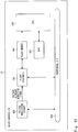
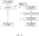
- Fig. 14 is a flowchart showing an example of the operation of the flash sequencer 700 during writing to the data memory unit 150. The operation is described by reference to Fig. 14 . It is assumed that erasing of the interrupt detection memory unit 152 has been performed prior to the operation of the flowchart shown in Fig. 14 , and " 1 " that is set during the erasing is stored as the interrupt detection flag value.
- Step 10 the flash sequencer 700 receives a write command to the data memory unit 150 and starts writing to the data memory unit 150.
- writing of the status flag of the status memory unit 151 is carried out simultaneously with writing to the data memory unit 150.
- the flash sequencer 700 continues processing until data writing is completed.
- the flash sequencer 700 starts writing of the interrupt detection flag.
- the flash sequencer 700 first interrupts writing to the data memory unit 150 in Step 11 (S11). To be specific, in this exemplary embodiment, the flash sequencer 700 interrupts writing to the data memory unit 150 and writing of the status memory unit 151. Next, in Step 12 (S12), the flash sequencer 700 performs writing of the interrupt detection flag. To be more specific, writing of the interrupt detection flag is carried out in the interrupt detection memory unit 152 corresponding to the data memory unit 150 where writing has been performed in Step 10. When writing of the interrupt detection flag is completed, "0" is stored as the interrupt detection flag value into the interrupt detection memory unit 152.
- the interrupt detection memory unit 152 that is read by the reference read mode and that stores the interrupt detection flag indicating whether an interruption of writing occurs or not is placed. It is thereby possible to determine whether there is an interruption of writing in the data memory unit 150 and the status memory unit 151. If the interrupt detection flag is read by the complementary read mode, when an interruption is detected and the interrupt detection flag is written in the past, "0" can be read even after erasing in the interrupt detection memory unit 152. This can cause a failure to determine the presence or absence of an interruption. On the other hand, because the interrupt detection memory unit 152 is read by the reference read mode in this exemplary embodiment, the value in the erased state is uniquely defined, thus preventing the above problem.
- writing is performed simultaneously and erasing is also performed simultaneously in the data memory unit 150 and the status memory unit 151 in this exemplary embodiment, writing may be performed separately, and erasing may be performed separately.
- a decrease in voltage is notified from the voltage monitoring circuit 600 included in the micro controller 10 to the flash sequencer 700, and the flash sequencer 700 controls processing after the notification is described as an example.
- this may be implemented by another configuration.
- a method for notifying a decrease in voltage may be any of the following three methods.
- Notification method 1 Detection is done by a voltage monitoring circuit inside the micro controller 10, and notification is given by an internal signal (the notification method described as the third exemplary embodiment).
- Notification method 2 Detection is done by a power supply control circuit outside the micro controller 10, and notification is given through an interrupt terminal of the micro controller 10.
- Notification method 3 Detection is done by a power supply control circuit outside the micro controller 10, and notification is given through a reset terminal of the micro controller 10.
- the voltage monitoring circuit and the power supply control circuit can be also referred to as a voltage detection unit (voltage detection circuit).
- a destination of notification about a decrease in voltage and a processing method after notification may be any of the following three methods, for example.
- Control method 1 Notification about a decrease in voltage is given to the flash sequencer 700.
- the flash sequencer 700 interrupts data writing and carries out writing of the interrupt detection flag (the control method described as the third exemplary embodiment).
- Control method 2 Notification about a decrease in voltage is given to an interrupt controller (not shown) of the micro controller 10. Interruption of data writing and writing of the interrupt detection flag are instructed to the flash sequencer 700 by software processing of the CPU 400, and writing of the interrupt detection flag is carried out.
- Control method 3 Notification about a decrease in voltage is given to a system control unit (not shown) of the micro controller 10. In the state where the elements other than the flash sequencer 700 and the flash memory 100 are reset, a signal indicating writing of the interrupt detection flag is output from the system control unit to the flash sequencer 700, and the flash sequencer 700 interrupts data writing and carries out writing of the interrupt detection flag.
- Combinations of the notification methods and the control methods described above may be the following five combinations, for example.
- an exemplary embodiment that combines the notification method 1 and the control method 1 an exemplary embodiment that combines the notification method 1 and the control method 2
- an exemplary embodiment that combines the notification method 2 and the control method 1 an exemplary embodiment that combines the notification method 2 and the control method 2
- an exemplary embodiment that combines the notification method 3 and the control method 3 may be implemented as an example of combinations.
- interrupt detection memory unit 152 is added to the flash memory 200 according to the second exemplary embodiment in the third exemplary embodiment, the interrupt detection memory unit 152 may be added to the flash memory 100 according to the first exemplary embodiment.
- the first to third embodiments can be combined as desirable by one of ordinary skill in the art.
Landscapes
- Engineering & Computer Science (AREA)
- Theoretical Computer Science (AREA)
- Microelectronics & Electronic Packaging (AREA)
- Human Computer Interaction (AREA)
- Physics & Mathematics (AREA)
- General Engineering & Computer Science (AREA)
- General Physics & Mathematics (AREA)
- Read Only Memory (AREA)
Claims (9)
- Eine Speichervorrichtung (1), die Folgendes umfasst:eine Datenspeicherschaltung (2, 150), die so konfiguriert ist, dass sie ein Paar von Flash-Speicherzellen (4) enthält, die durch einen komplementären Lesemodus gelesen werden, wobei 1-Bit-Daten in dem Paar von Flash-Speicherzellen gespeichert werden; undeine Statusspeicherschaltung (3, 151), die so konfiguriert ist, dass sie Flash-Speicherzellen (5) enthält, die durch einen Referenzlesemodus gelesen werden sollen, wobei die Speichervorrichtung (1) dadurch gekennzeichnet ist, dass ein Statusflag in den Flash-Speicherzellen gespeichert wird, wobeidie Statusspeicherschaltung (3, 151) eine Vielzahl von Flash-Speicherzellen enthält, in denen das Statusflag mit dem gleichen Wert gespeichert ist, unddie Speichervorrichtung ferner eine Bestimmungsschaltung (107, 108) umfasst, die so konfiguriert ist, dass sie einen Wert des Statusflags bestimmt, indem sie einen Summenstrom von Strömen, die durch die Vielzahl von Flash-Speicherzellen fließen, mit einem Referenzstrom vergleicht.
- Speichervorrichtung nach Anspruch 1, wobei die Bestimmungsschaltung (107, 108) eine erste Signalleitung (BL), die mit jeder der mehreren Flash-Speicherzellen verbunden ist, und eine zweite Signalleitung (IL), die mit einer Stromquelle verbunden ist, die so konfiguriert ist, dass sie den Referenzstrom liefert, vorlädt, die erste Signalleitung (BL) und die zweite Signalleitung (IL) durch den Summenstrom bzw. den Referenzstrom entlädt und den Summenstrom mit dem Referenzstrom vergleicht, indem sie eine Spannung der ersten Signalleitung (BL) mit einer Spannung der zweiten Signalleitung (IL) nach der Entladung vergleicht.
- Die Speichervorrichtung nach einem der Ansprüche 1 bis 2, weiter umfassend:
eine Ausgangsschaltung (111), die so konfiguriert ist, dass sie eine logische ODER-Verknüpfung zwischen einem Lesewert der Datenspeicherschaltung (2, 150) und einem Lesewert der Statusspeicherschaltung (3, 151) durchführt und ein Operationsergebnis als Leseergebnis der Datenspeicherschaltung ausgibt. - Die Speichervorrichtung nach einem der Ansprüche 1 bis 3, weiterhin umfassend:eine Unterbrechungserfassungs-Speicherschaltung (152), die so konfiguriert ist, dass sie eine Flash-Speicherzelle enthält, die durch den Referenzlesemodus gelesen werden soll, wobei ein Unterbrechungserfassungs-Flag anzeigt, ob eine Unterbrechung des Schreibens in der Flash-Speicherzelle gespeichert ist oder nicht;eine Spannungserfassungsschaltung (600), die konfiguriert ist, um zu erfassen, ob eine Stromversorgungsspannung gleich oder niedriger als ein spezifizierter Wert wird; undeine Steuerschaltung (700), die so konfiguriert ist, dass sie eine Steuerung zur Unterbrechung des Schreibens in die Datenspeicherschaltung durchführt und einen Wert schreibt, der eine Unterbrechung der Unterbrechungserfassungs-Speicherschaltung anzeigt, wenn die Spannungserfassungsschaltung erkennt, dass die Stromversorgungsspannung während des Schreibens in die Datenspeicherschaltung gleich oder niedriger als der angegebene Wert wird.
- Speichervorrichtung nach Anspruch 4, bei der die Steuerschaltung (700) eine Steuerung durchführt, um einen Wert zu schreiben, der eine Unterbrechung der Unterbrechungserfassungs-Speicherschaltung anzeigt, nachdem das Schreiben in die Datenspeicherschaltung unterbrochen wurde.
- Die Speichervorrichtung nach Anspruch 4 oder 5, wobei die Steuerschaltung (700) die Steuerung zum Schreiben eines Wertes durchführt, der eine Unterbrechung der Unterbrechungserkennungs-Speicherschaltung anzeigt.
die Spannungserfassungsschaltung (600) einen Speicher enthält, der so konfiguriert ist, dass er den angegebenen Wert speichert, und
der angegebene Wert geändert werden kann. - Die Speichereinrichtung nach einem der Ansprüche 1 bis 6, wobei die Datenspeicherschaltung (2, 150) und die Statusspeicherschaltung (3, 151) gleichzeitig gelöscht werden.
- Die Speichervorrichtung nach einem der Ansprüche 1 bis 7, wobei das Statusflag ein Flag ist, das einen Datenschreibstatus der Datenspeicherschaltung anzeigt.
- Ein Speicherverfahren, umfassend:Speichern von 1-Bit-Daten in einem Paar von Flash-Speicherzellen, die durch einen komplementären Lesemodus gelesen werden sollen; und wobei das Verfahren gekennzeichnet ist durchSpeichern eines Statusflags in jeder von mehreren Flash-Speicherzellen, die durch einen Referenzlesemodus gelesen werden sollen, wobeiin dem Schritt des Speicherns des Statusflags wird das Statusflag mit dem gleichen Wert in jeder der Vielzahl von Flash-Speicherzellen gespeichert, undferner mit einem Schritt zur Bestimmung eines Wertes des Statusflags durch Vergleich eines Summenstroms der durch die Mehrzahl der Flash-Speicherzellen fließenden Ströme mit einem Referenzstrom.
Applications Claiming Priority (1)
| Application Number | Priority Date | Filing Date | Title |
|---|---|---|---|
| JP2017054425A JP2018156713A (ja) | 2017-03-21 | 2017-03-21 | 記憶装置及び記憶方法 |
Publications (2)
| Publication Number | Publication Date |
|---|---|
| EP3379540A1 EP3379540A1 (de) | 2018-09-26 |
| EP3379540B1 true EP3379540B1 (de) | 2020-03-11 |
Family
ID=61626946
Family Applications (1)
| Application Number | Title | Priority Date | Filing Date |
|---|---|---|---|
| EP18161136.9A Active EP3379540B1 (de) | 2017-03-21 | 2018-03-12 | Speichervorrichtung und speicherverfahren |
Country Status (5)
| Country | Link |
|---|---|
| US (1) | US10366758B2 (de) |
| EP (1) | EP3379540B1 (de) |
| JP (1) | JP2018156713A (de) |
| KR (1) | KR102530403B1 (de) |
| CN (1) | CN108630278B (de) |
Families Citing this family (5)
| Publication number | Priority date | Publication date | Assignee | Title |
|---|---|---|---|---|
| US10255987B1 (en) * | 2017-10-11 | 2019-04-09 | Globalfoundries Inc. | Margin test for one-time programmable memory (OTPM) array with common mode current source |
| JP2019179799A (ja) * | 2018-03-30 | 2019-10-17 | ルネサスエレクトロニクス株式会社 | 半導体記憶装置 |
| CN110659150B (zh) * | 2019-10-10 | 2023-04-21 | 深圳芯邦科技股份有限公司 | 微控制单元内存的检测方法以及相关装置 |
| US20230395135A1 (en) * | 2022-06-01 | 2023-12-07 | Micron Technology, Inc. | Timing for operations in memory device storing bits in memory cell pairs |
| JPWO2024214291A1 (de) * | 2023-04-14 | 2024-10-17 |
Family Cites Families (12)
| Publication number | Priority date | Publication date | Assignee | Title |
|---|---|---|---|---|
| US5943263A (en) * | 1997-01-08 | 1999-08-24 | Micron Technology, Inc. | Apparatus and method for programming voltage protection in a non-volatile memory system |
| EP1514189A1 (de) * | 2002-06-20 | 2005-03-16 | Tokyo Electron Device Limited | Speicherbaustein, speicherverwaltungsverfahren und programm |
| JP4133166B2 (ja) | 2002-09-25 | 2008-08-13 | 株式会社ルネサステクノロジ | 不揮発性半導体記憶装置 |
| JP4941906B2 (ja) * | 2004-05-12 | 2012-05-30 | ローム株式会社 | 有機el駆動回路およびこれを用いる有機el表示装置 |
| JP2006048793A (ja) * | 2004-08-02 | 2006-02-16 | Sony Corp | メモリセルおよび半導体記憶装置 |
| JP5311784B2 (ja) | 2006-10-11 | 2013-10-09 | ルネサスエレクトロニクス株式会社 | 半導体装置 |
| KR100938092B1 (ko) * | 2008-03-10 | 2010-01-21 | 주식회사 하이닉스반도체 | 플래시 메모리 소자의 동작 방법 |
| JP2009272028A (ja) | 2008-04-07 | 2009-11-19 | Renesas Technology Corp | 半導体集積回路およびその動作方法 |
| JP6185589B2 (ja) * | 2013-08-15 | 2017-08-23 | ルネサスエレクトロニクス株式会社 | 半導体装置および半導体装置におけるデータ秘匿方法 |
| CN105474325B (zh) * | 2013-08-22 | 2019-08-02 | 瑞萨电子株式会社 | 将双单元的存储数据屏蔽而进行输出的半导体器件 |
| US9728330B2 (en) * | 2014-07-03 | 2017-08-08 | Ferfics Limited | Radio frequency switching system with improved linearity |
| JP6422273B2 (ja) | 2014-09-03 | 2018-11-14 | ルネサスエレクトロニクス株式会社 | 半導体装置 |
-
2017
- 2017-03-21 JP JP2017054425A patent/JP2018156713A/ja active Pending
-
2018
- 2018-02-20 US US15/900,516 patent/US10366758B2/en active Active
- 2018-03-12 EP EP18161136.9A patent/EP3379540B1/de active Active
- 2018-03-19 KR KR1020180031377A patent/KR102530403B1/ko active Active
- 2018-03-20 CN CN201810228747.0A patent/CN108630278B/zh active Active
Non-Patent Citations (1)
| Title |
|---|
| None * |
Also Published As
| Publication number | Publication date |
|---|---|
| US10366758B2 (en) | 2019-07-30 |
| KR20180106982A (ko) | 2018-10-01 |
| CN108630278B (zh) | 2023-11-10 |
| EP3379540A1 (de) | 2018-09-26 |
| JP2018156713A (ja) | 2018-10-04 |
| US20180277214A1 (en) | 2018-09-27 |
| KR102530403B1 (ko) | 2023-05-09 |
| CN108630278A (zh) | 2018-10-09 |
Similar Documents
| Publication | Publication Date | Title |
|---|---|---|
| EP3379540B1 (de) | Speichervorrichtung und speicherverfahren | |
| KR960012359B1 (ko) | 반도체 기억장치 | |
| US5898615A (en) | Semiconductor memory device having non-volatile memory cells connected in series | |
| US7889551B2 (en) | Page buffer of non-volatile memory device and programming method of non-volatile memory device | |
| US20100191900A1 (en) | Nonvolatile memory device and method of operating the same | |
| TWI699766B (zh) | 半導體記憶體裝置 | |
| KR20210145073A (ko) | 반도체 기억장치 및 판독 방법 | |
| US8582368B2 (en) | Non-volatile memory device and operating method of the same | |
| US8279678B2 (en) | Method of performing program verification operation using page buffer of nonvolatile memory device | |
| US7636258B2 (en) | Integrated circuits, memory controller, and memory modules | |
| KR100648277B1 (ko) | 프로그램 시간을 줄일 수 있는 플래시 메모리 장치 | |
| JPH11102592A (ja) | 不揮発性半導体記憶装置 | |
| JP4284247B2 (ja) | 不揮発性半導体記憶装置 | |
| US8275934B2 (en) | Nonvolatile memory device and cache read method using the same | |
| JPH07141320A (ja) | 電流読み出し方法及びマイクロコントローラ | |
| JP4251717B2 (ja) | 不揮発性半導体記憶装置 | |
| US7248503B2 (en) | Semiconductor nonvolatile storage device | |
| KR20140109106A (ko) | 반도체 장치 및 이의 동작 방법 | |
| KR100669349B1 (ko) | 플래시 메모리 장치 및 그것의 읽기 방법 | |
| JP6267497B2 (ja) | 半導体メモリの制御装置及び不安定メモリ領域の検出方法 | |
| JP2004039055A (ja) | 不揮発性半導体記憶装置 | |
| KR20080019115A (ko) | 플래시 메모리 장치 | |
| KR20120119331A (ko) | 메모리 및 이의 동작방법 | |
| KR20140029023A (ko) | 메모리 및 메모리 시스템 | |
| KR20240124081A (ko) | 패스 전압을 조절하는 메모리 장치 및 그 동작 방법 |
Legal Events
| Date | Code | Title | Description |
|---|---|---|---|
| PUAI | Public reference made under article 153(3) epc to a published international application that has entered the european phase |
Free format text: ORIGINAL CODE: 0009012 |
|
| STAA | Information on the status of an ep patent application or granted ep patent |
Free format text: STATUS: THE APPLICATION HAS BEEN PUBLISHED |
|
| AK | Designated contracting states |
Kind code of ref document: A1 Designated state(s): AL AT BE BG CH CY CZ DE DK EE ES FI FR GB GR HR HU IE IS IT LI LT LU LV MC MK MT NL NO PL PT RO RS SE SI SK SM TR |
|
| AX | Request for extension of the european patent |
Extension state: BA ME |
|
| STAA | Information on the status of an ep patent application or granted ep patent |
Free format text: STATUS: REQUEST FOR EXAMINATION WAS MADE |
|
| 17P | Request for examination filed |
Effective date: 20190326 |
|
| RBV | Designated contracting states (corrected) |
Designated state(s): AL AT BE BG CH CY CZ DE DK EE ES FI FR GB GR HR HU IE IS IT LI LT LU LV MC MK MT NL NO PL PT RO RS SE SI SK SM TR |
|
| RIC1 | Information provided on ipc code assigned before grant |
Ipc: G11C 7/10 20060101ALI20190723BHEP Ipc: G11C 16/04 20060101ALI20190723BHEP Ipc: G11C 16/14 20060101ALI20190723BHEP Ipc: G11C 7/06 20060101ALI20190723BHEP Ipc: G11C 16/10 20060101ALI20190723BHEP Ipc: G11C 16/26 20060101AFI20190723BHEP Ipc: G11C 16/30 20060101ALI20190723BHEP Ipc: G11C 16/28 20060101ALI20190723BHEP |
|
| GRAP | Despatch of communication of intention to grant a patent |
Free format text: ORIGINAL CODE: EPIDOSNIGR1 |
|
| STAA | Information on the status of an ep patent application or granted ep patent |
Free format text: STATUS: GRANT OF PATENT IS INTENDED |
|
| INTG | Intention to grant announced |
Effective date: 20191002 |
|
| GRAS | Grant fee paid |
Free format text: ORIGINAL CODE: EPIDOSNIGR3 |
|
| GRAA | (expected) grant |
Free format text: ORIGINAL CODE: 0009210 |
|
| STAA | Information on the status of an ep patent application or granted ep patent |
Free format text: STATUS: THE PATENT HAS BEEN GRANTED |
|
| AK | Designated contracting states |
Kind code of ref document: B1 Designated state(s): AL AT BE BG CH CY CZ DE DK EE ES FI FR GB GR HR HU IE IS IT LI LT LU LV MC MK MT NL NO PL PT RO RS SE SI SK SM TR |
|
| REG | Reference to a national code |
Ref country code: GB Ref legal event code: FG4D |
|
| REG | Reference to a national code |
Ref country code: CH Ref legal event code: EP |
|
| REG | Reference to a national code |
Ref country code: AT Ref legal event code: REF Ref document number: 1244123 Country of ref document: AT Kind code of ref document: T Effective date: 20200315 |
|
| REG | Reference to a national code |
Ref country code: DE Ref legal event code: R096 Ref document number: 602018002904 Country of ref document: DE |
|
| REG | Reference to a national code |
Ref country code: IE Ref legal event code: FG4D |
|
| PG25 | Lapsed in a contracting state [announced via postgrant information from national office to epo] |
Ref country code: FI Free format text: LAPSE BECAUSE OF FAILURE TO SUBMIT A TRANSLATION OF THE DESCRIPTION OR TO PAY THE FEE WITHIN THE PRESCRIBED TIME-LIMIT Effective date: 20200311 Ref country code: NO Free format text: LAPSE BECAUSE OF FAILURE TO SUBMIT A TRANSLATION OF THE DESCRIPTION OR TO PAY THE FEE WITHIN THE PRESCRIBED TIME-LIMIT Effective date: 20200611 Ref country code: RS Free format text: LAPSE BECAUSE OF FAILURE TO SUBMIT A TRANSLATION OF THE DESCRIPTION OR TO PAY THE FEE WITHIN THE PRESCRIBED TIME-LIMIT Effective date: 20200311 |
|
| REG | Reference to a national code |
Ref country code: NL Ref legal event code: MP Effective date: 20200311 |
|
| PG25 | Lapsed in a contracting state [announced via postgrant information from national office to epo] |
Ref country code: SE Free format text: LAPSE BECAUSE OF FAILURE TO SUBMIT A TRANSLATION OF THE DESCRIPTION OR TO PAY THE FEE WITHIN THE PRESCRIBED TIME-LIMIT Effective date: 20200311 Ref country code: LV Free format text: LAPSE BECAUSE OF FAILURE TO SUBMIT A TRANSLATION OF THE DESCRIPTION OR TO PAY THE FEE WITHIN THE PRESCRIBED TIME-LIMIT Effective date: 20200311 Ref country code: GR Free format text: LAPSE BECAUSE OF FAILURE TO SUBMIT A TRANSLATION OF THE DESCRIPTION OR TO PAY THE FEE WITHIN THE PRESCRIBED TIME-LIMIT Effective date: 20200612 Ref country code: HR Free format text: LAPSE BECAUSE OF FAILURE TO SUBMIT A TRANSLATION OF THE DESCRIPTION OR TO PAY THE FEE WITHIN THE PRESCRIBED TIME-LIMIT Effective date: 20200311 Ref country code: BG Free format text: LAPSE BECAUSE OF FAILURE TO SUBMIT A TRANSLATION OF THE DESCRIPTION OR TO PAY THE FEE WITHIN THE PRESCRIBED TIME-LIMIT Effective date: 20200611 |
|
| REG | Reference to a national code |
Ref country code: LT Ref legal event code: MG4D |
|
| PG25 | Lapsed in a contracting state [announced via postgrant information from national office to epo] |
Ref country code: NL Free format text: LAPSE BECAUSE OF FAILURE TO SUBMIT A TRANSLATION OF THE DESCRIPTION OR TO PAY THE FEE WITHIN THE PRESCRIBED TIME-LIMIT Effective date: 20200311 |
|
| PG25 | Lapsed in a contracting state [announced via postgrant information from national office to epo] |
Ref country code: EE Free format text: LAPSE BECAUSE OF FAILURE TO SUBMIT A TRANSLATION OF THE DESCRIPTION OR TO PAY THE FEE WITHIN THE PRESCRIBED TIME-LIMIT Effective date: 20200311 Ref country code: SM Free format text: LAPSE BECAUSE OF FAILURE TO SUBMIT A TRANSLATION OF THE DESCRIPTION OR TO PAY THE FEE WITHIN THE PRESCRIBED TIME-LIMIT Effective date: 20200311 Ref country code: RO Free format text: LAPSE BECAUSE OF FAILURE TO SUBMIT A TRANSLATION OF THE DESCRIPTION OR TO PAY THE FEE WITHIN THE PRESCRIBED TIME-LIMIT Effective date: 20200311 Ref country code: CZ Free format text: LAPSE BECAUSE OF FAILURE TO SUBMIT A TRANSLATION OF THE DESCRIPTION OR TO PAY THE FEE WITHIN THE PRESCRIBED TIME-LIMIT Effective date: 20200311 Ref country code: LT Free format text: LAPSE BECAUSE OF FAILURE TO SUBMIT A TRANSLATION OF THE DESCRIPTION OR TO PAY THE FEE WITHIN THE PRESCRIBED TIME-LIMIT Effective date: 20200311 Ref country code: PT Free format text: LAPSE BECAUSE OF FAILURE TO SUBMIT A TRANSLATION OF THE DESCRIPTION OR TO PAY THE FEE WITHIN THE PRESCRIBED TIME-LIMIT Effective date: 20200805 Ref country code: IS Free format text: LAPSE BECAUSE OF FAILURE TO SUBMIT A TRANSLATION OF THE DESCRIPTION OR TO PAY THE FEE WITHIN THE PRESCRIBED TIME-LIMIT Effective date: 20200711 Ref country code: SK Free format text: LAPSE BECAUSE OF FAILURE TO SUBMIT A TRANSLATION OF THE DESCRIPTION OR TO PAY THE FEE WITHIN THE PRESCRIBED TIME-LIMIT Effective date: 20200311 |
|
| REG | Reference to a national code |
Ref country code: AT Ref legal event code: MK05 Ref document number: 1244123 Country of ref document: AT Kind code of ref document: T Effective date: 20200311 |
|
| REG | Reference to a national code |
Ref country code: DE Ref legal event code: R097 Ref document number: 602018002904 Country of ref document: DE |
|
| REG | Reference to a national code |
Ref country code: BE Ref legal event code: MM Effective date: 20200331 |
|
| PG25 | Lapsed in a contracting state [announced via postgrant information from national office to epo] |
Ref country code: LU Free format text: LAPSE BECAUSE OF NON-PAYMENT OF DUE FEES Effective date: 20200312 Ref country code: MC Free format text: LAPSE BECAUSE OF FAILURE TO SUBMIT A TRANSLATION OF THE DESCRIPTION OR TO PAY THE FEE WITHIN THE PRESCRIBED TIME-LIMIT Effective date: 20200311 |
|
| PLBE | No opposition filed within time limit |
Free format text: ORIGINAL CODE: 0009261 |
|
| STAA | Information on the status of an ep patent application or granted ep patent |
Free format text: STATUS: NO OPPOSITION FILED WITHIN TIME LIMIT |
|
| PG25 | Lapsed in a contracting state [announced via postgrant information from national office to epo] |
Ref country code: ES Free format text: LAPSE BECAUSE OF FAILURE TO SUBMIT A TRANSLATION OF THE DESCRIPTION OR TO PAY THE FEE WITHIN THE PRESCRIBED TIME-LIMIT Effective date: 20200311 Ref country code: IT Free format text: LAPSE BECAUSE OF FAILURE TO SUBMIT A TRANSLATION OF THE DESCRIPTION OR TO PAY THE FEE WITHIN THE PRESCRIBED TIME-LIMIT Effective date: 20200311 Ref country code: AT Free format text: LAPSE BECAUSE OF FAILURE TO SUBMIT A TRANSLATION OF THE DESCRIPTION OR TO PAY THE FEE WITHIN THE PRESCRIBED TIME-LIMIT Effective date: 20200311 Ref country code: IE Free format text: LAPSE BECAUSE OF NON-PAYMENT OF DUE FEES Effective date: 20200312 Ref country code: DK Free format text: LAPSE BECAUSE OF FAILURE TO SUBMIT A TRANSLATION OF THE DESCRIPTION OR TO PAY THE FEE WITHIN THE PRESCRIBED TIME-LIMIT Effective date: 20200311 |
|
| 26N | No opposition filed |
Effective date: 20201214 |
|
| PG25 | Lapsed in a contracting state [announced via postgrant information from national office to epo] |
Ref country code: SI Free format text: LAPSE BECAUSE OF FAILURE TO SUBMIT A TRANSLATION OF THE DESCRIPTION OR TO PAY THE FEE WITHIN THE PRESCRIBED TIME-LIMIT Effective date: 20200311 Ref country code: BE Free format text: LAPSE BECAUSE OF NON-PAYMENT OF DUE FEES Effective date: 20200331 Ref country code: PL Free format text: LAPSE BECAUSE OF FAILURE TO SUBMIT A TRANSLATION OF THE DESCRIPTION OR TO PAY THE FEE WITHIN THE PRESCRIBED TIME-LIMIT Effective date: 20200311 |
|
| PG25 | Lapsed in a contracting state [announced via postgrant information from national office to epo] |
Ref country code: FR Free format text: LAPSE BECAUSE OF NON-PAYMENT OF DUE FEES Effective date: 20200511 |
|
| REG | Reference to a national code |
Ref country code: CH Ref legal event code: PL |
|
| PG25 | Lapsed in a contracting state [announced via postgrant information from national office to epo] |
Ref country code: CH Free format text: LAPSE BECAUSE OF NON-PAYMENT OF DUE FEES Effective date: 20210331 Ref country code: LI Free format text: LAPSE BECAUSE OF NON-PAYMENT OF DUE FEES Effective date: 20210331 |
|
| PG25 | Lapsed in a contracting state [announced via postgrant information from national office to epo] |
Ref country code: TR Free format text: LAPSE BECAUSE OF FAILURE TO SUBMIT A TRANSLATION OF THE DESCRIPTION OR TO PAY THE FEE WITHIN THE PRESCRIBED TIME-LIMIT Effective date: 20200311 Ref country code: MT Free format text: LAPSE BECAUSE OF FAILURE TO SUBMIT A TRANSLATION OF THE DESCRIPTION OR TO PAY THE FEE WITHIN THE PRESCRIBED TIME-LIMIT Effective date: 20200311 Ref country code: CY Free format text: LAPSE BECAUSE OF FAILURE TO SUBMIT A TRANSLATION OF THE DESCRIPTION OR TO PAY THE FEE WITHIN THE PRESCRIBED TIME-LIMIT Effective date: 20200311 |
|
| PG25 | Lapsed in a contracting state [announced via postgrant information from national office to epo] |
Ref country code: MK Free format text: LAPSE BECAUSE OF FAILURE TO SUBMIT A TRANSLATION OF THE DESCRIPTION OR TO PAY THE FEE WITHIN THE PRESCRIBED TIME-LIMIT Effective date: 20200311 Ref country code: AL Free format text: LAPSE BECAUSE OF FAILURE TO SUBMIT A TRANSLATION OF THE DESCRIPTION OR TO PAY THE FEE WITHIN THE PRESCRIBED TIME-LIMIT Effective date: 20200311 |
|
| GBPC | Gb: european patent ceased through non-payment of renewal fee |
Effective date: 20220312 |
|
| PG25 | Lapsed in a contracting state [announced via postgrant information from national office to epo] |
Ref country code: GB Free format text: LAPSE BECAUSE OF NON-PAYMENT OF DUE FEES Effective date: 20220312 |
|
| PGFP | Annual fee paid to national office [announced via postgrant information from national office to epo] |
Ref country code: DE Payment date: 20260320 Year of fee payment: 9 |