EP3376260B1 - Strahlungsdetektor und herstellungsverfahren für strahlungsdetektor - Google Patents
Strahlungsdetektor und herstellungsverfahren für strahlungsdetektor Download PDFInfo
- Publication number
- EP3376260B1 EP3376260B1 EP16864044.9A EP16864044A EP3376260B1 EP 3376260 B1 EP3376260 B1 EP 3376260B1 EP 16864044 A EP16864044 A EP 16864044A EP 3376260 B1 EP3376260 B1 EP 3376260B1
- Authority
- EP
- European Patent Office
- Prior art keywords
- absorption layer
- radiation
- layer
- radiation absorption
- radiation detector
- Prior art date
- Legal status (The legal status is an assumption and is not a legal conclusion. Google has not performed a legal analysis and makes no representation as to the accuracy of the status listed.)
- Active
Links
- 230000005855 radiation Effects 0.000 title claims description 198
- 238000004519 manufacturing process Methods 0.000 title claims description 17
- 239000002245 particle Substances 0.000 claims description 161
- 238000010521 absorption reaction Methods 0.000 claims description 146
- 239000004065 semiconductor Substances 0.000 claims description 95
- 229920005989 resin Polymers 0.000 claims description 45
- 239000011347 resin Substances 0.000 claims description 45
- 239000011230 binding agent Substances 0.000 claims description 38
- 239000003960 organic solvent Substances 0.000 claims description 22
- 230000005525 hole transport Effects 0.000 claims description 16
- 238000000576 coating method Methods 0.000 claims description 12
- 238000000034 method Methods 0.000 claims description 12
- 238000007650 screen-printing Methods 0.000 claims description 12
- 239000011248 coating agent Substances 0.000 claims description 11
- 239000000758 substrate Substances 0.000 claims description 11
- 239000013078 crystal Substances 0.000 claims description 7
- 238000010298 pulverizing process Methods 0.000 claims description 4
- 239000010410 layer Substances 0.000 description 166
- 239000000463 material Substances 0.000 description 31
- 238000002156 mixing Methods 0.000 description 19
- 230000007423 decrease Effects 0.000 description 16
- 239000000243 solution Substances 0.000 description 11
- -1 methylammonium lead halide Chemical class 0.000 description 10
- 229910000480 nickel oxide Inorganic materials 0.000 description 10
- 239000010409 thin film Substances 0.000 description 10
- 239000010408 film Substances 0.000 description 9
- 230000035945 sensitivity Effects 0.000 description 8
- 239000003990 capacitor Substances 0.000 description 7
- 239000011247 coating layer Substances 0.000 description 7
- 230000000694 effects Effects 0.000 description 7
- 230000006872 improvement Effects 0.000 description 7
- XOLBLPGZBRYERU-UHFFFAOYSA-N tin dioxide Chemical compound O=[Sn]=O XOLBLPGZBRYERU-UHFFFAOYSA-N 0.000 description 7
- 229910044991 metal oxide Inorganic materials 0.000 description 6
- 150000004706 metal oxides Chemical class 0.000 description 6
- 238000005507 spraying Methods 0.000 description 6
- 238000001035 drying Methods 0.000 description 5
- 229910003437 indium oxide Inorganic materials 0.000 description 5
- PJXISJQVUVHSOJ-UHFFFAOYSA-N indium(iii) oxide Chemical compound [O-2].[O-2].[O-2].[In+3].[In+3] PJXISJQVUVHSOJ-UHFFFAOYSA-N 0.000 description 5
- 239000007788 liquid Substances 0.000 description 5
- GNRSAWUEBMWBQH-UHFFFAOYSA-N oxonickel Chemical compound [Ni]=O GNRSAWUEBMWBQH-UHFFFAOYSA-N 0.000 description 5
- QPLDLSVMHZLSFG-UHFFFAOYSA-N Copper oxide Chemical compound [Cu]=O QPLDLSVMHZLSFG-UHFFFAOYSA-N 0.000 description 4
- UQSXHKLRYXJYBZ-UHFFFAOYSA-N Iron oxide Chemical compound [Fe]=O UQSXHKLRYXJYBZ-UHFFFAOYSA-N 0.000 description 4
- VYPSYNLAJGMNEJ-UHFFFAOYSA-N Silicium dioxide Chemical compound O=[Si]=O VYPSYNLAJGMNEJ-UHFFFAOYSA-N 0.000 description 4
- GWEVSGVZZGPLCZ-UHFFFAOYSA-N Titan oxide Chemical compound O=[Ti]=O GWEVSGVZZGPLCZ-UHFFFAOYSA-N 0.000 description 4
- 230000005540 biological transmission Effects 0.000 description 4
- 229910000420 cerium oxide Inorganic materials 0.000 description 4
- YBMRDBCBODYGJE-UHFFFAOYSA-N germanium dioxide Chemical compound O=[Ge]=O YBMRDBCBODYGJE-UHFFFAOYSA-N 0.000 description 4
- 229910000484 niobium oxide Inorganic materials 0.000 description 4
- BMMGVYCKOGBVEV-UHFFFAOYSA-N oxo(oxoceriooxy)cerium Chemical compound [Ce]=O.O=[Ce]=O BMMGVYCKOGBVEV-UHFFFAOYSA-N 0.000 description 4
- SIWVEOZUMHYXCS-UHFFFAOYSA-N oxo(oxoyttriooxy)yttrium Chemical compound O=[Y]O[Y]=O SIWVEOZUMHYXCS-UHFFFAOYSA-N 0.000 description 4
- RVTZCBVAJQQJTK-UHFFFAOYSA-N oxygen(2-);zirconium(4+) Chemical compound [O-2].[O-2].[Zr+4] RVTZCBVAJQQJTK-UHFFFAOYSA-N 0.000 description 4
- 229910052712 strontium Inorganic materials 0.000 description 4
- CIOAGBVUUVVLOB-UHFFFAOYSA-N strontium atom Chemical compound [Sr] CIOAGBVUUVVLOB-UHFFFAOYSA-N 0.000 description 4
- 229910001887 tin oxide Inorganic materials 0.000 description 4
- 229910001928 zirconium oxide Inorganic materials 0.000 description 4
- ZMXDDKWLCZADIW-UHFFFAOYSA-N N,N-Dimethylformamide Chemical compound CN(C)C=O ZMXDDKWLCZADIW-UHFFFAOYSA-N 0.000 description 3
- 239000004698 Polyethylene Substances 0.000 description 3
- 239000004642 Polyimide Substances 0.000 description 3
- 239000004372 Polyvinyl alcohol Substances 0.000 description 3
- RTAQQCXQSZGOHL-UHFFFAOYSA-N Titanium Chemical compound [Ti] RTAQQCXQSZGOHL-UHFFFAOYSA-N 0.000 description 3
- XLOMVQKBTHCTTD-UHFFFAOYSA-N Zinc monoxide Chemical compound [Zn]=O XLOMVQKBTHCTTD-UHFFFAOYSA-N 0.000 description 3
- NIXOWILDQLNWCW-UHFFFAOYSA-N acrylic acid group Chemical group C(C=C)(=O)O NIXOWILDQLNWCW-UHFFFAOYSA-N 0.000 description 3
- 229910052782 aluminium Inorganic materials 0.000 description 3
- XAGFODPZIPBFFR-UHFFFAOYSA-N aluminium Chemical compound [Al] XAGFODPZIPBFFR-UHFFFAOYSA-N 0.000 description 3
- 150000004820 halides Chemical class 0.000 description 3
- 238000003384 imaging method Methods 0.000 description 3
- 238000002347 injection Methods 0.000 description 3
- 239000007924 injection Substances 0.000 description 3
- 229920000515 polycarbonate Polymers 0.000 description 3
- 239000004417 polycarbonate Substances 0.000 description 3
- 229920000728 polyester Polymers 0.000 description 3
- 229920000573 polyethylene Polymers 0.000 description 3
- 229920001721 polyimide Polymers 0.000 description 3
- 239000004814 polyurethane Substances 0.000 description 3
- 229920002635 polyurethane Polymers 0.000 description 3
- 229920002451 polyvinyl alcohol Polymers 0.000 description 3
- 230000004044 response Effects 0.000 description 3
- 239000002904 solvent Substances 0.000 description 3
- 238000004528 spin coating Methods 0.000 description 3
- 230000001629 suppression Effects 0.000 description 3
- 229910052719 titanium Inorganic materials 0.000 description 3
- 239000010936 titanium Substances 0.000 description 3
- YEJRWHAVMIAJKC-UHFFFAOYSA-N 4-Butyrolactone Chemical compound O=C1CCCO1 YEJRWHAVMIAJKC-UHFFFAOYSA-N 0.000 description 2
- 239000005751 Copper oxide Substances 0.000 description 2
- SECXISVLQFMRJM-UHFFFAOYSA-N N-Methylpyrrolidone Chemical compound CN1CCCC1=O SECXISVLQFMRJM-UHFFFAOYSA-N 0.000 description 2
- XUIMIQQOPSSXEZ-UHFFFAOYSA-N Silicon Chemical compound [Si] XUIMIQQOPSSXEZ-UHFFFAOYSA-N 0.000 description 2
- UCKMPCXJQFINFW-UHFFFAOYSA-N Sulphide Chemical compound [S-2] UCKMPCXJQFINFW-UHFFFAOYSA-N 0.000 description 2
- ATJFFYVFTNAWJD-UHFFFAOYSA-N Tin Chemical compound [Sn] ATJFFYVFTNAWJD-UHFFFAOYSA-N 0.000 description 2
- HCHKCACWOHOZIP-UHFFFAOYSA-N Zinc Chemical compound [Zn] HCHKCACWOHOZIP-UHFFFAOYSA-N 0.000 description 2
- 238000000231 atomic layer deposition Methods 0.000 description 2
- 230000015572 biosynthetic process Effects 0.000 description 2
- 238000009835 boiling Methods 0.000 description 2
- 229910000428 cobalt oxide Inorganic materials 0.000 description 2
- UBEWDCMIDFGDOO-UHFFFAOYSA-N cobalt(II,III) oxide Inorganic materials [O-2].[O-2].[O-2].[O-2].[Co+2].[Co+3].[Co+3] UBEWDCMIDFGDOO-UHFFFAOYSA-N 0.000 description 2
- IVMYJDGYRUAWML-UHFFFAOYSA-N cobalt(ii) oxide Chemical compound [Co]=O IVMYJDGYRUAWML-UHFFFAOYSA-N 0.000 description 2
- 229910052681 coesite Inorganic materials 0.000 description 2
- 239000000084 colloidal system Substances 0.000 description 2
- 229910000431 copper oxide Inorganic materials 0.000 description 2
- BERDEBHAJNAUOM-UHFFFAOYSA-N copper(I) oxide Inorganic materials [Cu]O[Cu] BERDEBHAJNAUOM-UHFFFAOYSA-N 0.000 description 2
- 229910052906 cristobalite Inorganic materials 0.000 description 2
- KRFJLUBVMFXRPN-UHFFFAOYSA-N cuprous oxide Chemical compound [O-2].[Cu+].[Cu+] KRFJLUBVMFXRPN-UHFFFAOYSA-N 0.000 description 2
- 230000008034 disappearance Effects 0.000 description 2
- GNTDGMZSJNCJKK-UHFFFAOYSA-N divanadium pentaoxide Chemical compound O=[V](=O)O[V](=O)=O GNTDGMZSJNCJKK-UHFFFAOYSA-N 0.000 description 2
- 238000011049 filling Methods 0.000 description 2
- 239000011810 insulating material Substances 0.000 description 2
- JEIPFZHSYJVQDO-UHFFFAOYSA-N iron(III) oxide Inorganic materials O=[Fe]O[Fe]=O JEIPFZHSYJVQDO-UHFFFAOYSA-N 0.000 description 2
- MRELNEQAGSRDBK-UHFFFAOYSA-N lanthanum(3+);oxygen(2-) Chemical compound [O-2].[O-2].[O-2].[La+3].[La+3] MRELNEQAGSRDBK-UHFFFAOYSA-N 0.000 description 2
- 238000005259 measurement Methods 0.000 description 2
- 239000012046 mixed solvent Substances 0.000 description 2
- 239000004570 mortar (masonry) Substances 0.000 description 2
- 229910052758 niobium Inorganic materials 0.000 description 2
- 239000010955 niobium Substances 0.000 description 2
- GUCVJGMIXFAOAE-UHFFFAOYSA-N niobium atom Chemical compound [Nb] GUCVJGMIXFAOAE-UHFFFAOYSA-N 0.000 description 2
- URLJKFSTXLNXLG-UHFFFAOYSA-N niobium(5+);oxygen(2-) Chemical compound [O-2].[O-2].[O-2].[O-2].[O-2].[Nb+5].[Nb+5] URLJKFSTXLNXLG-UHFFFAOYSA-N 0.000 description 2
- BPUBBGLMJRNUCC-UHFFFAOYSA-N oxygen(2-);tantalum(5+) Chemical compound [O-2].[O-2].[O-2].[O-2].[O-2].[Ta+5].[Ta+5] BPUBBGLMJRNUCC-UHFFFAOYSA-N 0.000 description 2
- BASFCYQUMIYNBI-UHFFFAOYSA-N platinum Chemical compound [Pt] BASFCYQUMIYNBI-UHFFFAOYSA-N 0.000 description 2
- 229910052710 silicon Inorganic materials 0.000 description 2
- 239000010703 silicon Substances 0.000 description 2
- 239000000377 silicon dioxide Substances 0.000 description 2
- 238000005118 spray pyrolysis Methods 0.000 description 2
- 238000004544 sputter deposition Methods 0.000 description 2
- 229910052682 stishovite Inorganic materials 0.000 description 2
- 229910052718 tin Inorganic materials 0.000 description 2
- 239000011135 tin Substances 0.000 description 2
- OGIDPMRJRNCKJF-UHFFFAOYSA-N titanium oxide Inorganic materials [Ti]=O OGIDPMRJRNCKJF-UHFFFAOYSA-N 0.000 description 2
- 229910052905 tridymite Inorganic materials 0.000 description 2
- ZNOKGRXACCSDPY-UHFFFAOYSA-N tungsten trioxide Chemical compound O=[W](=O)=O ZNOKGRXACCSDPY-UHFFFAOYSA-N 0.000 description 2
- 238000007740 vapor deposition Methods 0.000 description 2
- 229910052725 zinc Inorganic materials 0.000 description 2
- 239000011701 zinc Substances 0.000 description 2
- 229910004613 CdTe Inorganic materials 0.000 description 1
- BQCADISMDOOEFD-UHFFFAOYSA-N Silver Chemical compound [Ag] BQCADISMDOOEFD-UHFFFAOYSA-N 0.000 description 1
- 230000009471 action Effects 0.000 description 1
- 150000001298 alcohols Chemical class 0.000 description 1
- 238000006243 chemical reaction Methods 0.000 description 1
- 229920001940 conductive polymer Polymers 0.000 description 1
- 239000004020 conductor Substances 0.000 description 1
- PDZKZMQQDCHTNF-UHFFFAOYSA-M copper(1+);thiocyanate Chemical compound [Cu+].[S-]C#N PDZKZMQQDCHTNF-UHFFFAOYSA-M 0.000 description 1
- LSXDOTMGLUJQCM-UHFFFAOYSA-M copper(i) iodide Chemical compound I[Cu] LSXDOTMGLUJQCM-UHFFFAOYSA-M 0.000 description 1
- BQVVSSAWECGTRN-UHFFFAOYSA-L copper;dithiocyanate Chemical compound [Cu+2].[S-]C#N.[S-]C#N BQVVSSAWECGTRN-UHFFFAOYSA-L 0.000 description 1
- 230000001066 destructive effect Effects 0.000 description 1
- 238000001514 detection method Methods 0.000 description 1
- 238000010586 diagram Methods 0.000 description 1
- 238000009826 distribution Methods 0.000 description 1
- 150000002170 ethers Chemical class 0.000 description 1
- LYCAIKOWRPUZTN-UHFFFAOYSA-N ethylene glycol Natural products OCCO LYCAIKOWRPUZTN-UHFFFAOYSA-N 0.000 description 1
- 230000005669 field effect Effects 0.000 description 1
- 239000011521 glass Substances 0.000 description 1
- 150000002334 glycols Chemical class 0.000 description 1
- PCHJSUWPFVWCPO-UHFFFAOYSA-N gold Chemical compound [Au] PCHJSUWPFVWCPO-UHFFFAOYSA-N 0.000 description 1
- 229910052737 gold Inorganic materials 0.000 description 1
- 239000010931 gold Substances 0.000 description 1
- 238000007731 hot pressing Methods 0.000 description 1
- WGCNASOHLSPBMP-UHFFFAOYSA-N hydroxyacetaldehyde Natural products OCC=O WGCNASOHLSPBMP-UHFFFAOYSA-N 0.000 description 1
- 238000007689 inspection Methods 0.000 description 1
- 239000012212 insulator Substances 0.000 description 1
- 150000002576 ketones Chemical class 0.000 description 1
- 239000002346 layers by function Substances 0.000 description 1
- 239000011159 matrix material Substances 0.000 description 1
- 229910052751 metal Inorganic materials 0.000 description 1
- 239000002184 metal Substances 0.000 description 1
- 239000011859 microparticle Substances 0.000 description 1
- 239000011259 mixed solution Substances 0.000 description 1
- JKQOBWVOAYFWKG-UHFFFAOYSA-N molybdenum trioxide Chemical compound O=[Mo](=O)=O JKQOBWVOAYFWKG-UHFFFAOYSA-N 0.000 description 1
- 239000002105 nanoparticle Substances 0.000 description 1
- 229910052697 platinum Inorganic materials 0.000 description 1
- 239000002243 precursor Substances 0.000 description 1
- 239000011164 primary particle Substances 0.000 description 1
- 230000006798 recombination Effects 0.000 description 1
- 238000005215 recombination Methods 0.000 description 1
- 229910052709 silver Inorganic materials 0.000 description 1
- 239000004332 silver Substances 0.000 description 1
- 230000032258 transport Effects 0.000 description 1
- YVTHLONGBIQYBO-UHFFFAOYSA-N zinc indium(3+) oxygen(2-) Chemical compound [O--].[Zn++].[In+3] YVTHLONGBIQYBO-UHFFFAOYSA-N 0.000 description 1
Images


Classifications
-
- H—ELECTRICITY
- H10—SEMICONDUCTOR DEVICES; ELECTRIC SOLID-STATE DEVICES NOT OTHERWISE PROVIDED FOR
- H10K—ORGANIC ELECTRIC SOLID-STATE DEVICES
- H10K39/00—Integrated devices, or assemblies of multiple devices, comprising at least one organic radiation-sensitive element covered by group H10K30/00
- H10K39/30—Devices controlled by radiation
- H10K39/32—Organic image sensors
-
- G—PHYSICS
- G01—MEASURING; TESTING
- G01T—MEASUREMENT OF NUCLEAR OR X-RADIATION
- G01T1/00—Measuring X-radiation, gamma radiation, corpuscular radiation, or cosmic radiation
- G01T1/16—Measuring radiation intensity
- G01T1/24—Measuring radiation intensity with semiconductor detectors
- G01T1/241—Electrode arrangements, e.g. continuous or parallel strips or the like
-
- G—PHYSICS
- G01—MEASURING; TESTING
- G01T—MEASUREMENT OF NUCLEAR OR X-RADIATION
- G01T1/00—Measuring X-radiation, gamma radiation, corpuscular radiation, or cosmic radiation
- G01T1/16—Measuring radiation intensity
- G01T1/24—Measuring radiation intensity with semiconductor detectors
-
- H—ELECTRICITY
- H01—ELECTRIC ELEMENTS
- H01G—CAPACITORS; CAPACITORS, RECTIFIERS, DETECTORS, SWITCHING DEVICES, LIGHT-SENSITIVE OR TEMPERATURE-SENSITIVE DEVICES OF THE ELECTROLYTIC TYPE
- H01G9/00—Electrolytic capacitors, rectifiers, detectors, switching devices, light-sensitive or temperature-sensitive devices; Processes of their manufacture
- H01G9/0029—Processes of manufacture
- H01G9/0036—Formation of the solid electrolyte layer
-
- H—ELECTRICITY
- H01—ELECTRIC ELEMENTS
- H01G—CAPACITORS; CAPACITORS, RECTIFIERS, DETECTORS, SWITCHING DEVICES, LIGHT-SENSITIVE OR TEMPERATURE-SENSITIVE DEVICES OF THE ELECTROLYTIC TYPE
- H01G9/00—Electrolytic capacitors, rectifiers, detectors, switching devices, light-sensitive or temperature-sensitive devices; Processes of their manufacture
- H01G9/20—Light-sensitive devices
- H01G9/2004—Light-sensitive devices characterised by the electrolyte, e.g. comprising an organic electrolyte
- H01G9/2009—Solid electrolytes
-
- H—ELECTRICITY
- H01—ELECTRIC ELEMENTS
- H01G—CAPACITORS; CAPACITORS, RECTIFIERS, DETECTORS, SWITCHING DEVICES, LIGHT-SENSITIVE OR TEMPERATURE-SENSITIVE DEVICES OF THE ELECTROLYTIC TYPE
- H01G9/00—Electrolytic capacitors, rectifiers, detectors, switching devices, light-sensitive or temperature-sensitive devices; Processes of their manufacture
- H01G9/20—Light-sensitive devices
- H01G9/2004—Light-sensitive devices characterised by the electrolyte, e.g. comprising an organic electrolyte
- H01G9/2018—Light-sensitive devices characterised by the electrolyte, e.g. comprising an organic electrolyte characterised by the ionic charge transport species, e.g. redox shuttles
-
- H—ELECTRICITY
- H01—ELECTRIC ELEMENTS
- H01L—SEMICONDUCTOR DEVICES NOT COVERED BY CLASS H10
- H01L27/00—Devices consisting of a plurality of semiconductor or other solid-state components formed in or on a common substrate
- H01L27/14—Devices consisting of a plurality of semiconductor or other solid-state components formed in or on a common substrate including semiconductor components sensitive to infrared radiation, light, electromagnetic radiation of shorter wavelength or corpuscular radiation and specially adapted either for the conversion of the energy of such radiation into electrical energy or for the control of electrical energy by such radiation
- H01L27/144—Devices controlled by radiation
- H01L27/146—Imager structures
-
- H—ELECTRICITY
- H10—SEMICONDUCTOR DEVICES; ELECTRIC SOLID-STATE DEVICES NOT OTHERWISE PROVIDED FOR
- H10K—ORGANIC ELECTRIC SOLID-STATE DEVICES
- H10K30/00—Organic devices sensitive to infrared radiation, light, electromagnetic radiation of shorter wavelength or corpuscular radiation
- H10K30/30—Organic devices sensitive to infrared radiation, light, electromagnetic radiation of shorter wavelength or corpuscular radiation comprising bulk heterojunctions, e.g. interpenetrating networks of donor and acceptor material domains
- H10K30/35—Organic devices sensitive to infrared radiation, light, electromagnetic radiation of shorter wavelength or corpuscular radiation comprising bulk heterojunctions, e.g. interpenetrating networks of donor and acceptor material domains comprising inorganic nanostructures, e.g. CdSe nanoparticles
-
- H—ELECTRICITY
- H10—SEMICONDUCTOR DEVICES; ELECTRIC SOLID-STATE DEVICES NOT OTHERWISE PROVIDED FOR
- H10K—ORGANIC ELECTRIC SOLID-STATE DEVICES
- H10K39/00—Integrated devices, or assemblies of multiple devices, comprising at least one organic radiation-sensitive element covered by group H10K30/00
- H10K39/30—Devices controlled by radiation
- H10K39/36—Devices specially adapted for detecting X-ray radiation
-
- H—ELECTRICITY
- H10—SEMICONDUCTOR DEVICES; ELECTRIC SOLID-STATE DEVICES NOT OTHERWISE PROVIDED FOR
- H10K—ORGANIC ELECTRIC SOLID-STATE DEVICES
- H10K71/00—Manufacture or treatment specially adapted for the organic devices covered by this subclass
- H10K71/10—Deposition of organic active material
- H10K71/12—Deposition of organic active material using liquid deposition, e.g. spin coating
- H10K71/13—Deposition of organic active material using liquid deposition, e.g. spin coating using printing techniques, e.g. ink-jet printing or screen printing
-
- H—ELECTRICITY
- H10—SEMICONDUCTOR DEVICES; ELECTRIC SOLID-STATE DEVICES NOT OTHERWISE PROVIDED FOR
- H10K—ORGANIC ELECTRIC SOLID-STATE DEVICES
- H10K71/00—Manufacture or treatment specially adapted for the organic devices covered by this subclass
- H10K71/20—Changing the shape of the active layer in the devices, e.g. patterning
-
- H—ELECTRICITY
- H10—SEMICONDUCTOR DEVICES; ELECTRIC SOLID-STATE DEVICES NOT OTHERWISE PROVIDED FOR
- H10K—ORGANIC ELECTRIC SOLID-STATE DEVICES
- H10K85/00—Organic materials used in the body or electrodes of devices covered by this subclass
- H10K85/50—Organic perovskites; Hybrid organic-inorganic perovskites [HOIP], e.g. CH3NH3PbI3
-
- Y—GENERAL TAGGING OF NEW TECHNOLOGICAL DEVELOPMENTS; GENERAL TAGGING OF CROSS-SECTIONAL TECHNOLOGIES SPANNING OVER SEVERAL SECTIONS OF THE IPC; TECHNICAL SUBJECTS COVERED BY FORMER USPC CROSS-REFERENCE ART COLLECTIONS [XRACs] AND DIGESTS
- Y02—TECHNOLOGIES OR APPLICATIONS FOR MITIGATION OR ADAPTATION AGAINST CLIMATE CHANGE
- Y02E—REDUCTION OF GREENHOUSE GAS [GHG] EMISSIONS, RELATED TO ENERGY GENERATION, TRANSMISSION OR DISTRIBUTION
- Y02E10/00—Energy generation through renewable energy sources
- Y02E10/50—Photovoltaic [PV] energy
- Y02E10/542—Dye sensitized solar cells
-
- Y—GENERAL TAGGING OF NEW TECHNOLOGICAL DEVELOPMENTS; GENERAL TAGGING OF CROSS-SECTIONAL TECHNOLOGIES SPANNING OVER SEVERAL SECTIONS OF THE IPC; TECHNICAL SUBJECTS COVERED BY FORMER USPC CROSS-REFERENCE ART COLLECTIONS [XRACs] AND DIGESTS
- Y02—TECHNOLOGIES OR APPLICATIONS FOR MITIGATION OR ADAPTATION AGAINST CLIMATE CHANGE
- Y02E—REDUCTION OF GREENHOUSE GAS [GHG] EMISSIONS, RELATED TO ENERGY GENERATION, TRANSMISSION OR DISTRIBUTION
- Y02E10/00—Energy generation through renewable energy sources
- Y02E10/50—Photovoltaic [PV] energy
- Y02E10/549—Organic PV cells
-
- Y—GENERAL TAGGING OF NEW TECHNOLOGICAL DEVELOPMENTS; GENERAL TAGGING OF CROSS-SECTIONAL TECHNOLOGIES SPANNING OVER SEVERAL SECTIONS OF THE IPC; TECHNICAL SUBJECTS COVERED BY FORMER USPC CROSS-REFERENCE ART COLLECTIONS [XRACs] AND DIGESTS
- Y02—TECHNOLOGIES OR APPLICATIONS FOR MITIGATION OR ADAPTATION AGAINST CLIMATE CHANGE
- Y02P—CLIMATE CHANGE MITIGATION TECHNOLOGIES IN THE PRODUCTION OR PROCESSING OF GOODS
- Y02P70/00—Climate change mitigation technologies in the production process for final industrial or consumer products
- Y02P70/50—Manufacturing or production processes characterised by the final manufactured product
Definitions
- a thickness of the radiation absorption layer as described above is, for example, preferably 100 ⁇ m or more from the viewpoint of improvement of radiation absorption efficiency.
- a spray coating of a perovskite material only a film of about several tens of nm can be formed in one step. Therefore, the radiation detector described in Non Patent Literature 1 is not realistic from the viewpoint of mass producibility.
- the radiation absorption layer may further include inorganic semiconductor particles other than the perovskite structure particles. Accordingly, it is possible to increase mobility of charge (electrons and holes) generated in the radiation absorption layer due to absorption of radiation and to obtain sufficient sensitivity and response characteristics.
- a method for manufacturing a radiation detector includes a first step of preparing a coating solution containing perovskite structure particles, a binder resin, and an organic solvent; a second step of forming a radiation absorption layer on one side with respect to a substrate including a charge collection electrode through screen printing using the coating solution after the first step, the radiation absorption layer containing the perovskite structure particles and the binder resin; and a third step of forming a voltage application electrode on the one side with respect to the radiation absorption layer after the second step, a bias voltage being applied to the voltage application electrode such that a potential difference is generated between the voltage application electrode and the charge collection electrode.
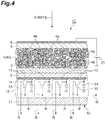
- the radiation absorption layer 4 is disposed on one side with respect to the panel 10 to cover all the pixels P of the panel 10 when viewed in a incidence direction of X-rays.
- the radiation absorption layer 4 contains perovskite structure particles 4p and a binder resin 4r.
- the voltage application electrode 6 is disposed on one side with respect to the radiation absorption layer 4 to cover all the pixels P of the panel 10 when viewed in the incidence direction of the X-rays.
- the voltage application electrode 6 is formed of a metal such as aluminum, gold, silver, platinum, or titanium, a conductive metal oxide such as tin-doped indium oxide (ITO), fluorine-added tin oxide (FTO), tin oxide (SnO 2 ), indium zinc oxide (IZO), or zinc oxide (ZnO), or an organic conductive material containing a conductive polymer or the like.
- a bias voltage is applied to the voltage application electrode 6 by a bias voltage supply power supply 21 so that a negative potential difference is generated between the voltage application electrode 6 and the charge collection electrode 13 of each pixel P.
- CH 3 NH 2 I and PbX 2 are mixed in an organic solvent in a molar ratio of 1:1 to prepare methylammonium lead halide (here, CH 3 NH 3 PbX 3 ) that is the perovskite structure particle 4p.
- methylammonium lead halide here, CH 3 NH 3 PbX 3
- the solution is distilled to obtain a perovskite structure crystal block formed of the methylammonium lead halide.
- the perovskite structure crystal block is pulverized to obtain the perovskite structure particle 4p.
- the perovskite structure particles 4p and the inorganic semiconductor particles 4s are added to the solution in which the binder resin 4r has been dissolved, and are completely dissolved to adjust the coating liquid containing the perovskite structure particles 4p, the inorganic semiconductor particles 4s, the binder resin 4r, and the organic solvent.
- the conductivity type of the inorganic semiconductor particle 4s and the conductivity type of the dense layer 2 and the porous layer 3 are the same n type.
- the electrons generated in the radiation absorption layer 4 due to the absorption of the X-rays can be more smoothly moved to the charge collection electrode 13.
- the bias voltage may be applied to the voltage application electrode 6 so that a positive potential difference is generated between the voltage application electrode 6 and the charge collection electrode 13.
- the dense layer 2 and the porous layer 3 to be formed of a p-type semiconductor material (for example, copper oxide (Cu 2 O, CuO), nickel oxide (NiO), or cobalt oxide (CoO, Co 3 O 4 ).
Landscapes
- Engineering & Computer Science (AREA)
- Power Engineering (AREA)
- Physics & Mathematics (AREA)
- Chemical & Material Sciences (AREA)
- Microelectronics & Electronic Packaging (AREA)
- General Physics & Mathematics (AREA)
- Electromagnetism (AREA)
- Electrochemistry (AREA)
- Chemical Kinetics & Catalysis (AREA)
- Computer Hardware Design (AREA)
- Condensed Matter Physics & Semiconductors (AREA)
- Molecular Biology (AREA)
- Spectroscopy & Molecular Physics (AREA)
- Health & Medical Sciences (AREA)
- High Energy & Nuclear Physics (AREA)
- Life Sciences & Earth Sciences (AREA)
- Manufacturing & Machinery (AREA)
- Crystallography & Structural Chemistry (AREA)
- Inorganic Chemistry (AREA)
- Nanotechnology (AREA)
- Materials Engineering (AREA)
- Measurement Of Radiation (AREA)
- Solid State Image Pick-Up Elements (AREA)
Claims (8)
- Strahlungsdetektor (1A, 1B, 1C), umfassend:ein Substrat (11), das eine Ladungssammelelektrode (13) beinhaltet;eine Strahlungsabsorptionsschicht (4), die an einer Seite in Bezug auf das Substrat (11) angeordnet ist; undeine Spannungsanwendungselektrode (6), die an der einen Seite in Bezug auf die Strahlungsabsorptionsschicht (4) angeordnet ist, wobei eine Vorspannung auf die Spannungsanwendungselektrode angewendet ist, sodass ein Potentialunterschied zwischen der Spannungsanwendungselektrode (6) und der Ladungssammelelektrode (13) erzeugt ist,gekennzeichnet durch die Strahlungsabsorptionsschicht (4), die Perovskitstrukturpartikel (4p) und ein Bindemittelharz (4r) beinhaltet.
- Strahlungsdetektor (1B, 1C) nach Anspruch 1, wobei die Strahlungsabsorptionsschicht (4) weiter andere anorganische Halbleiterpartikel (4s) als die Perovskitstrukturpartikel (4p) beinhaltet.
- Strahlungsdetektor (1B, 1C) nach Anspruch 2, wobei ein Durchschnittspartikeldurchmesser der Perovskitstrukturpartikel (4p) größer als ein Durchschnittspartikeldurchmesser der anorganischen Halbleiterpartikel (4s) ist.
- Strahlungsdetektor (1B, 1C) nach Anspruch 2 oder 3, weiter umfassend eine Halbleiterladungssammelschicht (3), die zwischen dem Substrat (11) und der Strahlungsabsorptionsschicht (4) angeordnet ist.
- Strahlungsdetektor (1B, 1C) nach Anspruch 4, wobei ein Leitfähigkeitstyp der anorganischen Halbleiterpartikel (4s) und ein Leitfähigkeitstyp der Halbleiterladungssammelschicht (3) derselbe sind.
- Strahlungsdetektor (1A, 1B, 1C) nach einem der Ansprüche 1 bis 5, weiter umfassend eine Lochtransportschicht (5), die zwischen der Strahlungsabsorptionsschicht (4) und der Spannungsanwendungselektrode (6) angeordnet ist.
- Verfahren zur Herstellung eines Strahlungsdetektors (1A, 1B, 1C), wobei das Verfahren umfasst:einen ersten Schritt zum Vorbereiten einer Beschichtungslösung, die Perovskitstrukturpartikel (4p), ein Bindemittelharz (4r) und ein organisches Lösemittel enthält;einen zweiten Schritt zum Bilden einer Strahlungsabsorptionsschicht (4) an einer Seite in Bezug auf ein Substrat (11), beinhaltend eine Ladungssammelelektrode (13), durch Siebdruck unter Verwendung der Beschichtungslösung nach dem ersten Schritt, wobei die Strahlungsabsorptionsschicht (4) die Perovskitstrukturpartikel (4p) und das Bindemittelharz (4r) enthält; undeinen dritten Schritt zum Bilden einer Spannungsanwendungselektrode (6) an der einen Seite in Bezug auf die Strahlungsabsorptionsschicht (4) nach dem zweiten Schritt,wobei eine Vorspannung auf die Spannungsanwendungselektrode (6) angewendet wird, sodass ein Potentialunterschied zwischen der Spannungsanwendungselektrode (6) und der Ladungssammelelektrode (13) erzeugt ist.
- Verfahren nach Anspruch 7, weiter umfassend einen Schritt zum Pulverisieren eines Perovskitstrukturkristallblocks, um die Perovskitstrukturpartikel (4p) vor dem ersten Schritt zu erhalten.
Applications Claiming Priority (2)
| Application Number | Priority Date | Filing Date | Title |
|---|---|---|---|
| JP2015219211A JP6535271B2 (ja) | 2015-11-09 | 2015-11-09 | 放射線検出器、及び放射線検出器の製造方法 |
| PCT/JP2016/082051 WO2017082081A1 (ja) | 2015-11-09 | 2016-10-28 | 放射線検出器、及び放射線検出器の製造方法 |
Publications (3)
| Publication Number | Publication Date |
|---|---|
| EP3376260A1 EP3376260A1 (de) | 2018-09-19 |
| EP3376260A4 EP3376260A4 (de) | 2019-07-17 |
| EP3376260B1 true EP3376260B1 (de) | 2020-06-03 |
Family
ID=58696117
Family Applications (1)
| Application Number | Title | Priority Date | Filing Date |
|---|---|---|---|
| EP16864044.9A Active EP3376260B1 (de) | 2015-11-09 | 2016-10-28 | Strahlungsdetektor und herstellungsverfahren für strahlungsdetektor |
Country Status (6)
| Country | Link |
|---|---|
| US (1) | US10816681B2 (de) |
| EP (1) | EP3376260B1 (de) |
| JP (1) | JP6535271B2 (de) |
| KR (1) | KR102480425B1 (de) |
| CN (1) | CN108351428B (de) |
| WO (1) | WO2017082081A1 (de) |
Families Citing this family (15)
| Publication number | Priority date | Publication date | Assignee | Title |
|---|---|---|---|---|
| CN109285846B (zh) * | 2017-07-20 | 2023-10-13 | 松下知识产权经营株式会社 | 光传感器及使用它的光检测装置 |
| EP3474339A1 (de) | 2017-10-20 | 2019-04-24 | Siemens Healthcare GmbH | Röntgenbildsensor mit haftvermittler-zwischenschicht und weichgesinterter perovskit-aktivschicht |
| CN108318907B (zh) * | 2018-02-01 | 2019-10-01 | 北京京东方光电科技有限公司 | X射线探测面板及其制造方法和x射线探测装置 |
| JP7264402B2 (ja) | 2018-06-26 | 2023-04-25 | 国立大学法人京都大学 | 放射線検出器、及び放射線検出器の製造方法 |
| CN109206449B (zh) * | 2018-08-01 | 2020-05-15 | 南京航空航天大学 | 一种有机-无机钙钛矿晶体材料及其制备方法与应用 |
| EP3863059A1 (de) * | 2020-02-04 | 2021-08-11 | Siemens Healthcare GmbH | Perowskit-basierte detektoren mit erhöhter adhäsion |
| EP3863054A1 (de) | 2020-02-04 | 2021-08-11 | Siemens Healthcare GmbH | Multiple spektrale detektoren mittels strukturierter perowskite |
| CN111286252A (zh) * | 2020-03-09 | 2020-06-16 | 长沙而道新能源科技有限公司 | 一种抗辐射防腐涂料及其制备方法 |
| EP3916819A1 (de) * | 2020-05-29 | 2021-12-01 | Nederlandse Organisatie voor toegepast- natuurwetenschappelijk Onderzoek TNO | Perowskitschicht |
| JP2023127003A (ja) * | 2020-08-06 | 2023-09-13 | パナソニックIpマネジメント株式会社 | 電離放射線変換デバイスおよび電離放射線の検出方法 |
| KR102474979B1 (ko) * | 2021-01-12 | 2022-12-06 | 주식회사 파프리카랩 | 피부 부착형 방사선 측정 장치를 이용한 방사선 피폭 모니터링 시스템 |
| CN113035900B (zh) * | 2021-02-26 | 2023-02-10 | 深圳先进技术研究院 | 一种直接型电磁辐射探测器及制备方法 |
| EP4068363B1 (de) | 2021-03-30 | 2023-06-07 | Siemens Healthcare GmbH | Strahlungsdetektor mit gestossenen absorberkacheln ohne tote bereiche |
| CN113970779A (zh) * | 2021-10-12 | 2022-01-25 | 华北电力大学 | 一种钙钛矿填充微孔面板形成的微结构闪烁屏及制备方法 |
| EP4180845A1 (de) | 2021-11-11 | 2023-05-17 | Siemens Healthcare GmbH | Strahlungsdetektor mit lasergeschnittenen absorberplatten |
Family Cites Families (14)
| Publication number | Priority date | Publication date | Assignee | Title |
|---|---|---|---|---|
| JP3669860B2 (ja) * | 1999-03-10 | 2005-07-13 | Tdk株式会社 | 積層薄膜 |
| JP3779604B2 (ja) * | 2001-01-15 | 2006-05-31 | 独立行政法人科学技術振興機構 | 放射線検出装置 |
| JP3714918B2 (ja) * | 2001-07-31 | 2005-11-09 | 独立行政法人科学技術振興機構 | 放射線検出装置 |
| JP4269859B2 (ja) * | 2003-09-10 | 2009-05-27 | 株式会社島津製作所 | 放射線検出器 |
| US9834858B2 (en) * | 2004-11-08 | 2017-12-05 | Tohoku Techno Arch Co., Ltd. | Pr-containing scintillator single crystal, method of manufacturing the same, radiation detector, and inspection apparatus |
| JP5233119B2 (ja) * | 2004-12-21 | 2013-07-10 | 日立金属株式会社 | 蛍光材料およびその製造方法、蛍光材料を用いた放射線検出器、並びにx線ct装置 |
| KR101064856B1 (ko) * | 2006-02-23 | 2011-09-14 | 가부시키가이샤 시마즈세이사쿠쇼 | 방사선 검출기 |
| JP2008039548A (ja) * | 2006-08-04 | 2008-02-21 | Ohyo Koken Kogyo Co Ltd | シンチレーション検出器 |
| JP5521412B2 (ja) * | 2008-07-31 | 2014-06-11 | 日立金属株式会社 | 蛍光材料およびそれを用いたシンチレータ並びに放射線検出器 |
| JP2011054638A (ja) * | 2009-08-31 | 2011-03-17 | Fujifilm Corp | 光導電層の製造方法 |
| JP6066608B2 (ja) | 2011-07-27 | 2017-01-25 | キヤノン株式会社 | 相分離構造を有するシンチレータおよびそれを用いた放射線検出器 |
| US9812660B2 (en) * | 2013-12-19 | 2017-11-07 | Nutech Ventures | Method for single crystal growth of photovoltaic perovskite material and devices |
| DE102015225145A1 (de) * | 2015-12-14 | 2017-06-14 | Siemens Healthcare Gmbh | Perowskitpartikel für die Herstellung von Röntgendetektoren mittels Abscheidung aus der Trockenphase |
| DE102016205818A1 (de) * | 2016-04-07 | 2017-10-12 | Siemens Healthcare Gmbh | Vorrichtung und Verfahren zum Detektieren von Röntgenstrahlung |
-
2015
- 2015-11-09 JP JP2015219211A patent/JP6535271B2/ja active Active
-
2016
- 2016-10-28 KR KR1020187014557A patent/KR102480425B1/ko active IP Right Grant
- 2016-10-28 EP EP16864044.9A patent/EP3376260B1/de active Active
- 2016-10-28 CN CN201680065192.1A patent/CN108351428B/zh active Active
- 2016-10-28 WO PCT/JP2016/082051 patent/WO2017082081A1/ja active Application Filing
- 2016-10-28 US US15/773,618 patent/US10816681B2/en active Active
Non-Patent Citations (1)
| Title |
|---|
| None * |
Also Published As
| Publication number | Publication date |
|---|---|
| EP3376260A1 (de) | 2018-09-19 |
| JP6535271B2 (ja) | 2019-06-26 |
| CN108351428A (zh) | 2018-07-31 |
| EP3376260A4 (de) | 2019-07-17 |
| US10816681B2 (en) | 2020-10-27 |
| US20200257006A1 (en) | 2020-08-13 |
| KR102480425B1 (ko) | 2022-12-23 |
| JP2017090186A (ja) | 2017-05-25 |
| CN108351428B (zh) | 2021-08-17 |
| WO2017082081A1 (ja) | 2017-05-18 |
| KR20180081742A (ko) | 2018-07-17 |
Similar Documents
| Publication | Publication Date | Title |
|---|---|---|
| EP3376260B1 (de) | Strahlungsdetektor und herstellungsverfahren für strahlungsdetektor | |
| Basiricò et al. | Detection of X‐rays by solution‐processed cesium‐containing mixed triple cation perovskite thin films | |
| KR101819757B1 (ko) | 평판 x-선 영상기에서의 포토다이오드 및 기타 센서 구조물, 및 박막 전자 회로에 기초하여 평판 x-선 영상기에서의 포토다이오드 및 기타 센서 구조물의 토폴로지적 균일성을 향상시키는 방법 | |
| US7902512B1 (en) | Coplanar high fill factor pixel architecture | |
| US8791419B2 (en) | High charge capacity pixel architecture, photoelectric conversion apparatus, radiation image pickup system and methods for same | |
| JP4547760B2 (ja) | 放射線検出器および放射線撮像装置 | |
| US7122803B2 (en) | Amorphous selenium flat panel x-ray imager for tomosynthesis and static imaging | |
| CA2669678C (en) | Photodetector/imaging device with avalanche gain | |
| US7233005B2 (en) | Amorphous selenium flat panel x-ray imager for tomosynthesis and static imaging | |
| US8735839B2 (en) | Pastes for photoelectric conversion layers of X-ray detectors, X-ray detectors and methods of manufacturing the same | |
| US8252617B2 (en) | Continuous large area imaging and display arrays using readout arrays fabricated in silicon-on-glass substrates | |
| CN109585477B (zh) | 平板探测器结构及其制备方法 | |
| WO2015186657A1 (ja) | 半導体装置およびその製造方法 | |
| US7632539B2 (en) | Method for manufacturing photoconductive layers that constitute radiation imaging panels | |
| US8232531B2 (en) | Corrosion barrier layer for photoconductive X-ray imagers | |
| JP2019506733A (ja) | 上部透明電極を有する光電子アレイデバイス | |
| US9348037B2 (en) | X-ray pixels including double photoconductors and X-ray detectors including the X-ray pixels | |
| WO2016130978A1 (en) | Radiation detector | |
| CN112928137B (zh) | 有机光电平板探测器 | |
| CN115084176A (zh) | 直接型多能平板探测器及其制备方法 | |
| Shrestha et al. | A perspective on the device physics of lead halide perovskite semiconducting detector for gamma and x-ray sensing | |
| KR101829992B1 (ko) | 페로브스카이트 화합물을 포함하는 포토컨덕터를 구비한 엑스선 검출기 | |
| JPWO2013065212A1 (ja) | 放射線検出器 | |
| CN112736201A (zh) | 间接型平板探测器及其制备方法 |
Legal Events
| Date | Code | Title | Description |
|---|---|---|---|
| STAA | Information on the status of an ep patent application or granted ep patent |
Free format text: STATUS: THE INTERNATIONAL PUBLICATION HAS BEEN MADE |
|
| PUAI | Public reference made under article 153(3) epc to a published international application that has entered the european phase |
Free format text: ORIGINAL CODE: 0009012 |
|
| STAA | Information on the status of an ep patent application or granted ep patent |
Free format text: STATUS: REQUEST FOR EXAMINATION WAS MADE |
|
| 17P | Request for examination filed |
Effective date: 20180509 |
|
| AK | Designated contracting states |
Kind code of ref document: A1 Designated state(s): AL AT BE BG CH CY CZ DE DK EE ES FI FR GB GR HR HU IE IS IT LI LT LU LV MC MK MT NL NO PL PT RO RS SE SI SK SM TR |
|
| AX | Request for extension of the european patent |
Extension state: BA ME |
|
| DAV | Request for validation of the european patent (deleted) | ||
| DAX | Request for extension of the european patent (deleted) | ||
| A4 | Supplementary search report drawn up and despatched |
Effective date: 20190618 |
|
| RIC1 | Information provided on ipc code assigned before grant |
Ipc: H01L 27/30 20060101ALI20190612BHEP Ipc: H01L 27/144 20060101AFI20190612BHEP Ipc: H01L 27/146 20060101ALI20190612BHEP Ipc: H01L 51/42 20060101ALI20190612BHEP |
|
| REG | Reference to a national code |
Ref country code: DE Ref legal event code: R079 Ref document number: 602016037702 Country of ref document: DE Free format text: PREVIOUS MAIN CLASS: G01T0001240000 Ipc: H01L0027300000 |
|
| GRAP | Despatch of communication of intention to grant a patent |
Free format text: ORIGINAL CODE: EPIDOSNIGR1 |
|
| STAA | Information on the status of an ep patent application or granted ep patent |
Free format text: STATUS: GRANT OF PATENT IS INTENDED |
|
| RIC1 | Information provided on ipc code assigned before grant |
Ipc: H01L 27/30 20060101AFI20191118BHEP Ipc: H01L 51/42 20060101ALI20191118BHEP |
|
| INTG | Intention to grant announced |
Effective date: 20191204 |
|
| RIN1 | Information on inventor provided before grant (corrected) |
Inventor name: IZAWA, TOSHIYUKI Inventor name: YAMAMOTO, KOEI Inventor name: ABE, KEIJI |
|
| GRAS | Grant fee paid |
Free format text: ORIGINAL CODE: EPIDOSNIGR3 |
|
| GRAJ | Information related to disapproval of communication of intention to grant by the applicant or resumption of examination proceedings by the epo deleted |
Free format text: ORIGINAL CODE: EPIDOSDIGR1 |
|
| GRAL | Information related to payment of fee for publishing/printing deleted |
Free format text: ORIGINAL CODE: EPIDOSDIGR3 |
|
| STAA | Information on the status of an ep patent application or granted ep patent |
Free format text: STATUS: REQUEST FOR EXAMINATION WAS MADE |
|
| INTC | Intention to grant announced (deleted) | ||
| GRAJ | Information related to disapproval of communication of intention to grant by the applicant or resumption of examination proceedings by the epo deleted |
Free format text: ORIGINAL CODE: EPIDOSDIGR1 |
|
| GRAP | Despatch of communication of intention to grant a patent |
Free format text: ORIGINAL CODE: EPIDOSNIGR1 |
|
| GRAJ | Information related to disapproval of communication of intention to grant by the applicant or resumption of examination proceedings by the epo deleted |
Free format text: ORIGINAL CODE: EPIDOSDIGR1 |
|
| GRAR | Information related to intention to grant a patent recorded |
Free format text: ORIGINAL CODE: EPIDOSNIGR71 |
|
| STAA | Information on the status of an ep patent application or granted ep patent |
Free format text: STATUS: GRANT OF PATENT IS INTENDED |
|
| GRAA | (expected) grant |
Free format text: ORIGINAL CODE: 0009210 |
|
| STAA | Information on the status of an ep patent application or granted ep patent |
Free format text: STATUS: THE PATENT HAS BEEN GRANTED |
|
| INTG | Intention to grant announced |
Effective date: 20200422 |
|
| AK | Designated contracting states |
Kind code of ref document: B1 Designated state(s): AL AT BE BG CH CY CZ DE DK EE ES FI FR GB GR HR HU IE IS IT LI LT LU LV MC MK MT NL NO PL PT RO RS SE SI SK SM TR |
|
| REG | Reference to a national code |
Ref country code: GB Ref legal event code: FG4D |
|
| REG | Reference to a national code |
Ref country code: CH Ref legal event code: EP Ref country code: AT Ref legal event code: REF Ref document number: 1277919 Country of ref document: AT Kind code of ref document: T Effective date: 20200615 |
|
| REG | Reference to a national code |
Ref country code: DE Ref legal event code: R096 Ref document number: 602016037702 Country of ref document: DE |
|
| REG | Reference to a national code |
Ref country code: FI Ref legal event code: FGE |
|
| REG | Reference to a national code |
Ref country code: LT Ref legal event code: MG4D |
|
| PG25 | Lapsed in a contracting state [announced via postgrant information from national office to epo] |
Ref country code: SE Free format text: LAPSE BECAUSE OF FAILURE TO SUBMIT A TRANSLATION OF THE DESCRIPTION OR TO PAY THE FEE WITHIN THE PRESCRIBED TIME-LIMIT Effective date: 20200603 Ref country code: NO Free format text: LAPSE BECAUSE OF FAILURE TO SUBMIT A TRANSLATION OF THE DESCRIPTION OR TO PAY THE FEE WITHIN THE PRESCRIBED TIME-LIMIT Effective date: 20200903 Ref country code: LT Free format text: LAPSE BECAUSE OF FAILURE TO SUBMIT A TRANSLATION OF THE DESCRIPTION OR TO PAY THE FEE WITHIN THE PRESCRIBED TIME-LIMIT Effective date: 20200603 Ref country code: GR Free format text: LAPSE BECAUSE OF FAILURE TO SUBMIT A TRANSLATION OF THE DESCRIPTION OR TO PAY THE FEE WITHIN THE PRESCRIBED TIME-LIMIT Effective date: 20200904 |
|
| REG | Reference to a national code |
Ref country code: NL Ref legal event code: MP Effective date: 20200603 |
|
| PG25 | Lapsed in a contracting state [announced via postgrant information from national office to epo] |
Ref country code: BG Free format text: LAPSE BECAUSE OF FAILURE TO SUBMIT A TRANSLATION OF THE DESCRIPTION OR TO PAY THE FEE WITHIN THE PRESCRIBED TIME-LIMIT Effective date: 20200903 Ref country code: RS Free format text: LAPSE BECAUSE OF FAILURE TO SUBMIT A TRANSLATION OF THE DESCRIPTION OR TO PAY THE FEE WITHIN THE PRESCRIBED TIME-LIMIT Effective date: 20200603 Ref country code: LV Free format text: LAPSE BECAUSE OF FAILURE TO SUBMIT A TRANSLATION OF THE DESCRIPTION OR TO PAY THE FEE WITHIN THE PRESCRIBED TIME-LIMIT Effective date: 20200603 Ref country code: HR Free format text: LAPSE BECAUSE OF FAILURE TO SUBMIT A TRANSLATION OF THE DESCRIPTION OR TO PAY THE FEE WITHIN THE PRESCRIBED TIME-LIMIT Effective date: 20200603 |
|
| REG | Reference to a national code |
Ref country code: AT Ref legal event code: MK05 Ref document number: 1277919 Country of ref document: AT Kind code of ref document: T Effective date: 20200603 |
|
| PG25 | Lapsed in a contracting state [announced via postgrant information from national office to epo] |
Ref country code: AL Free format text: LAPSE BECAUSE OF FAILURE TO SUBMIT A TRANSLATION OF THE DESCRIPTION OR TO PAY THE FEE WITHIN THE PRESCRIBED TIME-LIMIT Effective date: 20200603 Ref country code: NL Free format text: LAPSE BECAUSE OF FAILURE TO SUBMIT A TRANSLATION OF THE DESCRIPTION OR TO PAY THE FEE WITHIN THE PRESCRIBED TIME-LIMIT Effective date: 20200603 |
|
| PG25 | Lapsed in a contracting state [announced via postgrant information from national office to epo] |
Ref country code: EE Free format text: LAPSE BECAUSE OF FAILURE TO SUBMIT A TRANSLATION OF THE DESCRIPTION OR TO PAY THE FEE WITHIN THE PRESCRIBED TIME-LIMIT Effective date: 20200603 Ref country code: SM Free format text: LAPSE BECAUSE OF FAILURE TO SUBMIT A TRANSLATION OF THE DESCRIPTION OR TO PAY THE FEE WITHIN THE PRESCRIBED TIME-LIMIT Effective date: 20200603 Ref country code: AT Free format text: LAPSE BECAUSE OF FAILURE TO SUBMIT A TRANSLATION OF THE DESCRIPTION OR TO PAY THE FEE WITHIN THE PRESCRIBED TIME-LIMIT Effective date: 20200603 Ref country code: IT Free format text: LAPSE BECAUSE OF FAILURE TO SUBMIT A TRANSLATION OF THE DESCRIPTION OR TO PAY THE FEE WITHIN THE PRESCRIBED TIME-LIMIT Effective date: 20200603 Ref country code: PT Free format text: LAPSE BECAUSE OF FAILURE TO SUBMIT A TRANSLATION OF THE DESCRIPTION OR TO PAY THE FEE WITHIN THE PRESCRIBED TIME-LIMIT Effective date: 20201006 Ref country code: RO Free format text: LAPSE BECAUSE OF FAILURE TO SUBMIT A TRANSLATION OF THE DESCRIPTION OR TO PAY THE FEE WITHIN THE PRESCRIBED TIME-LIMIT Effective date: 20200603 Ref country code: CZ Free format text: LAPSE BECAUSE OF FAILURE TO SUBMIT A TRANSLATION OF THE DESCRIPTION OR TO PAY THE FEE WITHIN THE PRESCRIBED TIME-LIMIT Effective date: 20200603 Ref country code: ES Free format text: LAPSE BECAUSE OF FAILURE TO SUBMIT A TRANSLATION OF THE DESCRIPTION OR TO PAY THE FEE WITHIN THE PRESCRIBED TIME-LIMIT Effective date: 20200603 |
|
| PG25 | Lapsed in a contracting state [announced via postgrant information from national office to epo] |
Ref country code: PL Free format text: LAPSE BECAUSE OF FAILURE TO SUBMIT A TRANSLATION OF THE DESCRIPTION OR TO PAY THE FEE WITHIN THE PRESCRIBED TIME-LIMIT Effective date: 20200603 Ref country code: SK Free format text: LAPSE BECAUSE OF FAILURE TO SUBMIT A TRANSLATION OF THE DESCRIPTION OR TO PAY THE FEE WITHIN THE PRESCRIBED TIME-LIMIT Effective date: 20200603 Ref country code: IS Free format text: LAPSE BECAUSE OF FAILURE TO SUBMIT A TRANSLATION OF THE DESCRIPTION OR TO PAY THE FEE WITHIN THE PRESCRIBED TIME-LIMIT Effective date: 20201003 |
|
| REG | Reference to a national code |
Ref country code: DE Ref legal event code: R097 Ref document number: 602016037702 Country of ref document: DE |
|
| PLBE | No opposition filed within time limit |
Free format text: ORIGINAL CODE: 0009261 |
|
| STAA | Information on the status of an ep patent application or granted ep patent |
Free format text: STATUS: NO OPPOSITION FILED WITHIN TIME LIMIT |
|
| PG25 | Lapsed in a contracting state [announced via postgrant information from national office to epo] |
Ref country code: DK Free format text: LAPSE BECAUSE OF FAILURE TO SUBMIT A TRANSLATION OF THE DESCRIPTION OR TO PAY THE FEE WITHIN THE PRESCRIBED TIME-LIMIT Effective date: 20200603 |
|
| 26N | No opposition filed |
Effective date: 20210304 |
|
| PG25 | Lapsed in a contracting state [announced via postgrant information from national office to epo] |
Ref country code: SI Free format text: LAPSE BECAUSE OF FAILURE TO SUBMIT A TRANSLATION OF THE DESCRIPTION OR TO PAY THE FEE WITHIN THE PRESCRIBED TIME-LIMIT Effective date: 20200603 |
|
| REG | Reference to a national code |
Ref country code: CH Ref legal event code: PL |
|
| PG25 | Lapsed in a contracting state [announced via postgrant information from national office to epo] |
Ref country code: LU Free format text: LAPSE BECAUSE OF NON-PAYMENT OF DUE FEES Effective date: 20201028 Ref country code: MC Free format text: LAPSE BECAUSE OF FAILURE TO SUBMIT A TRANSLATION OF THE DESCRIPTION OR TO PAY THE FEE WITHIN THE PRESCRIBED TIME-LIMIT Effective date: 20200603 |
|
| REG | Reference to a national code |
Ref country code: BE Ref legal event code: MM Effective date: 20201031 |
|
| PG25 | Lapsed in a contracting state [announced via postgrant information from national office to epo] |
Ref country code: CH Free format text: LAPSE BECAUSE OF NON-PAYMENT OF DUE FEES Effective date: 20201031 Ref country code: BE Free format text: LAPSE BECAUSE OF NON-PAYMENT OF DUE FEES Effective date: 20201031 Ref country code: LI Free format text: LAPSE BECAUSE OF NON-PAYMENT OF DUE FEES Effective date: 20201031 |
|
| PG25 | Lapsed in a contracting state [announced via postgrant information from national office to epo] |
Ref country code: IE Free format text: LAPSE BECAUSE OF NON-PAYMENT OF DUE FEES Effective date: 20201028 |
|
| PG25 | Lapsed in a contracting state [announced via postgrant information from national office to epo] |
Ref country code: TR Free format text: LAPSE BECAUSE OF FAILURE TO SUBMIT A TRANSLATION OF THE DESCRIPTION OR TO PAY THE FEE WITHIN THE PRESCRIBED TIME-LIMIT Effective date: 20200603 Ref country code: MT Free format text: LAPSE BECAUSE OF FAILURE TO SUBMIT A TRANSLATION OF THE DESCRIPTION OR TO PAY THE FEE WITHIN THE PRESCRIBED TIME-LIMIT Effective date: 20200603 Ref country code: CY Free format text: LAPSE BECAUSE OF FAILURE TO SUBMIT A TRANSLATION OF THE DESCRIPTION OR TO PAY THE FEE WITHIN THE PRESCRIBED TIME-LIMIT Effective date: 20200603 |
|
| PG25 | Lapsed in a contracting state [announced via postgrant information from national office to epo] |
Ref country code: MK Free format text: LAPSE BECAUSE OF FAILURE TO SUBMIT A TRANSLATION OF THE DESCRIPTION OR TO PAY THE FEE WITHIN THE PRESCRIBED TIME-LIMIT Effective date: 20200603 |
|
| REG | Reference to a national code |
Ref country code: DE Ref legal event code: R079 Ref document number: 602016037702 Country of ref document: DE Free format text: PREVIOUS MAIN CLASS: H01L0027300000 Ipc: H10K0039000000 |
|
| P01 | Opt-out of the competence of the unified patent court (upc) registered |
Effective date: 20230509 |
|
| PGFP | Annual fee paid to national office [announced via postgrant information from national office to epo] |
Ref country code: GB Payment date: 20230907 Year of fee payment: 8 |
|
| PGFP | Annual fee paid to national office [announced via postgrant information from national office to epo] |
Ref country code: FR Payment date: 20230911 Year of fee payment: 8 |
|
| PGFP | Annual fee paid to national office [announced via postgrant information from national office to epo] |
Ref country code: FI Payment date: 20231011 Year of fee payment: 8 Ref country code: DE Payment date: 20230906 Year of fee payment: 8 |