EP3376260B1 - Radiation detector and manufacturing method for radiation detector - Google Patents
Radiation detector and manufacturing method for radiation detector Download PDFInfo
- Publication number
- EP3376260B1 EP3376260B1 EP16864044.9A EP16864044A EP3376260B1 EP 3376260 B1 EP3376260 B1 EP 3376260B1 EP 16864044 A EP16864044 A EP 16864044A EP 3376260 B1 EP3376260 B1 EP 3376260B1
- Authority
- EP
- European Patent Office
- Prior art keywords
- absorption layer
- radiation
- layer
- radiation absorption
- radiation detector
- Prior art date
- Legal status (The legal status is an assumption and is not a legal conclusion. Google has not performed a legal analysis and makes no representation as to the accuracy of the status listed.)
- Active
Links
- 230000005855 radiation Effects 0.000 title claims description 198
- 238000004519 manufacturing process Methods 0.000 title claims description 17
- 239000002245 particle Substances 0.000 claims description 161
- 238000010521 absorption reaction Methods 0.000 claims description 146
- 239000004065 semiconductor Substances 0.000 claims description 95
- 229920005989 resin Polymers 0.000 claims description 45
- 239000011347 resin Substances 0.000 claims description 45
- 239000011230 binding agent Substances 0.000 claims description 38
- 239000003960 organic solvent Substances 0.000 claims description 22
- 230000005525 hole transport Effects 0.000 claims description 16
- 238000000576 coating method Methods 0.000 claims description 12
- 238000000034 method Methods 0.000 claims description 12
- 238000007650 screen-printing Methods 0.000 claims description 12
- 239000011248 coating agent Substances 0.000 claims description 11
- 239000000758 substrate Substances 0.000 claims description 11
- 239000013078 crystal Substances 0.000 claims description 7
- 238000010298 pulverizing process Methods 0.000 claims description 4
- 239000010410 layer Substances 0.000 description 166
- 239000000463 material Substances 0.000 description 31
- 238000002156 mixing Methods 0.000 description 19
- 230000007423 decrease Effects 0.000 description 16
- 239000000243 solution Substances 0.000 description 11
- -1 methylammonium lead halide Chemical class 0.000 description 10
- 229910000480 nickel oxide Inorganic materials 0.000 description 10
- 239000010409 thin film Substances 0.000 description 10
- 239000010408 film Substances 0.000 description 9
- 230000035945 sensitivity Effects 0.000 description 8
- 239000003990 capacitor Substances 0.000 description 7
- 239000011247 coating layer Substances 0.000 description 7
- 230000000694 effects Effects 0.000 description 7
- 230000006872 improvement Effects 0.000 description 7
- XOLBLPGZBRYERU-UHFFFAOYSA-N tin dioxide Chemical compound O=[Sn]=O XOLBLPGZBRYERU-UHFFFAOYSA-N 0.000 description 7
- 229910044991 metal oxide Inorganic materials 0.000 description 6
- 150000004706 metal oxides Chemical class 0.000 description 6
- 238000005507 spraying Methods 0.000 description 6
- 238000001035 drying Methods 0.000 description 5
- 229910003437 indium oxide Inorganic materials 0.000 description 5
- PJXISJQVUVHSOJ-UHFFFAOYSA-N indium(iii) oxide Chemical compound [O-2].[O-2].[O-2].[In+3].[In+3] PJXISJQVUVHSOJ-UHFFFAOYSA-N 0.000 description 5
- 239000007788 liquid Substances 0.000 description 5
- GNRSAWUEBMWBQH-UHFFFAOYSA-N oxonickel Chemical compound [Ni]=O GNRSAWUEBMWBQH-UHFFFAOYSA-N 0.000 description 5
- QPLDLSVMHZLSFG-UHFFFAOYSA-N Copper oxide Chemical compound [Cu]=O QPLDLSVMHZLSFG-UHFFFAOYSA-N 0.000 description 4
- UQSXHKLRYXJYBZ-UHFFFAOYSA-N Iron oxide Chemical compound [Fe]=O UQSXHKLRYXJYBZ-UHFFFAOYSA-N 0.000 description 4
- VYPSYNLAJGMNEJ-UHFFFAOYSA-N Silicium dioxide Chemical compound O=[Si]=O VYPSYNLAJGMNEJ-UHFFFAOYSA-N 0.000 description 4
- GWEVSGVZZGPLCZ-UHFFFAOYSA-N Titan oxide Chemical compound O=[Ti]=O GWEVSGVZZGPLCZ-UHFFFAOYSA-N 0.000 description 4
- 230000005540 biological transmission Effects 0.000 description 4
- 229910000420 cerium oxide Inorganic materials 0.000 description 4
- YBMRDBCBODYGJE-UHFFFAOYSA-N germanium dioxide Chemical compound O=[Ge]=O YBMRDBCBODYGJE-UHFFFAOYSA-N 0.000 description 4
- 229910000484 niobium oxide Inorganic materials 0.000 description 4
- BMMGVYCKOGBVEV-UHFFFAOYSA-N oxo(oxoceriooxy)cerium Chemical compound [Ce]=O.O=[Ce]=O BMMGVYCKOGBVEV-UHFFFAOYSA-N 0.000 description 4
- SIWVEOZUMHYXCS-UHFFFAOYSA-N oxo(oxoyttriooxy)yttrium Chemical compound O=[Y]O[Y]=O SIWVEOZUMHYXCS-UHFFFAOYSA-N 0.000 description 4
- RVTZCBVAJQQJTK-UHFFFAOYSA-N oxygen(2-);zirconium(4+) Chemical compound [O-2].[O-2].[Zr+4] RVTZCBVAJQQJTK-UHFFFAOYSA-N 0.000 description 4
- 229910052712 strontium Inorganic materials 0.000 description 4
- CIOAGBVUUVVLOB-UHFFFAOYSA-N strontium atom Chemical compound [Sr] CIOAGBVUUVVLOB-UHFFFAOYSA-N 0.000 description 4
- 229910001887 tin oxide Inorganic materials 0.000 description 4
- 229910001928 zirconium oxide Inorganic materials 0.000 description 4
- ZMXDDKWLCZADIW-UHFFFAOYSA-N N,N-Dimethylformamide Chemical compound CN(C)C=O ZMXDDKWLCZADIW-UHFFFAOYSA-N 0.000 description 3
- 239000004698 Polyethylene Substances 0.000 description 3
- 239000004642 Polyimide Substances 0.000 description 3
- 239000004372 Polyvinyl alcohol Substances 0.000 description 3
- RTAQQCXQSZGOHL-UHFFFAOYSA-N Titanium Chemical compound [Ti] RTAQQCXQSZGOHL-UHFFFAOYSA-N 0.000 description 3
- XLOMVQKBTHCTTD-UHFFFAOYSA-N Zinc monoxide Chemical compound [Zn]=O XLOMVQKBTHCTTD-UHFFFAOYSA-N 0.000 description 3
- NIXOWILDQLNWCW-UHFFFAOYSA-N acrylic acid group Chemical group C(C=C)(=O)O NIXOWILDQLNWCW-UHFFFAOYSA-N 0.000 description 3
- 229910052782 aluminium Inorganic materials 0.000 description 3
- XAGFODPZIPBFFR-UHFFFAOYSA-N aluminium Chemical compound [Al] XAGFODPZIPBFFR-UHFFFAOYSA-N 0.000 description 3
- 150000004820 halides Chemical class 0.000 description 3
- 238000003384 imaging method Methods 0.000 description 3
- 238000002347 injection Methods 0.000 description 3
- 239000007924 injection Substances 0.000 description 3
- 229920000515 polycarbonate Polymers 0.000 description 3
- 239000004417 polycarbonate Substances 0.000 description 3
- 229920000728 polyester Polymers 0.000 description 3
- 229920000573 polyethylene Polymers 0.000 description 3
- 229920001721 polyimide Polymers 0.000 description 3
- 239000004814 polyurethane Substances 0.000 description 3
- 229920002635 polyurethane Polymers 0.000 description 3
- 229920002451 polyvinyl alcohol Polymers 0.000 description 3
- 230000004044 response Effects 0.000 description 3
- 239000002904 solvent Substances 0.000 description 3
- 238000004528 spin coating Methods 0.000 description 3
- 230000001629 suppression Effects 0.000 description 3
- 229910052719 titanium Inorganic materials 0.000 description 3
- 239000010936 titanium Substances 0.000 description 3
- YEJRWHAVMIAJKC-UHFFFAOYSA-N 4-Butyrolactone Chemical compound O=C1CCCO1 YEJRWHAVMIAJKC-UHFFFAOYSA-N 0.000 description 2
- 239000005751 Copper oxide Substances 0.000 description 2
- SECXISVLQFMRJM-UHFFFAOYSA-N N-Methylpyrrolidone Chemical compound CN1CCCC1=O SECXISVLQFMRJM-UHFFFAOYSA-N 0.000 description 2
- XUIMIQQOPSSXEZ-UHFFFAOYSA-N Silicon Chemical compound [Si] XUIMIQQOPSSXEZ-UHFFFAOYSA-N 0.000 description 2
- UCKMPCXJQFINFW-UHFFFAOYSA-N Sulphide Chemical compound [S-2] UCKMPCXJQFINFW-UHFFFAOYSA-N 0.000 description 2
- ATJFFYVFTNAWJD-UHFFFAOYSA-N Tin Chemical compound [Sn] ATJFFYVFTNAWJD-UHFFFAOYSA-N 0.000 description 2
- HCHKCACWOHOZIP-UHFFFAOYSA-N Zinc Chemical compound [Zn] HCHKCACWOHOZIP-UHFFFAOYSA-N 0.000 description 2
- 238000000231 atomic layer deposition Methods 0.000 description 2
- 230000015572 biosynthetic process Effects 0.000 description 2
- 238000009835 boiling Methods 0.000 description 2
- 229910000428 cobalt oxide Inorganic materials 0.000 description 2
- UBEWDCMIDFGDOO-UHFFFAOYSA-N cobalt(II,III) oxide Inorganic materials [O-2].[O-2].[O-2].[O-2].[Co+2].[Co+3].[Co+3] UBEWDCMIDFGDOO-UHFFFAOYSA-N 0.000 description 2
- IVMYJDGYRUAWML-UHFFFAOYSA-N cobalt(ii) oxide Chemical compound [Co]=O IVMYJDGYRUAWML-UHFFFAOYSA-N 0.000 description 2
- 229910052681 coesite Inorganic materials 0.000 description 2
- 239000000084 colloidal system Substances 0.000 description 2
- 229910000431 copper oxide Inorganic materials 0.000 description 2
- BERDEBHAJNAUOM-UHFFFAOYSA-N copper(I) oxide Inorganic materials [Cu]O[Cu] BERDEBHAJNAUOM-UHFFFAOYSA-N 0.000 description 2
- 229910052906 cristobalite Inorganic materials 0.000 description 2
- KRFJLUBVMFXRPN-UHFFFAOYSA-N cuprous oxide Chemical compound [O-2].[Cu+].[Cu+] KRFJLUBVMFXRPN-UHFFFAOYSA-N 0.000 description 2
- 230000008034 disappearance Effects 0.000 description 2
- GNTDGMZSJNCJKK-UHFFFAOYSA-N divanadium pentaoxide Chemical compound O=[V](=O)O[V](=O)=O GNTDGMZSJNCJKK-UHFFFAOYSA-N 0.000 description 2
- 238000011049 filling Methods 0.000 description 2
- 239000011810 insulating material Substances 0.000 description 2
- JEIPFZHSYJVQDO-UHFFFAOYSA-N iron(III) oxide Inorganic materials O=[Fe]O[Fe]=O JEIPFZHSYJVQDO-UHFFFAOYSA-N 0.000 description 2
- MRELNEQAGSRDBK-UHFFFAOYSA-N lanthanum(3+);oxygen(2-) Chemical compound [O-2].[O-2].[O-2].[La+3].[La+3] MRELNEQAGSRDBK-UHFFFAOYSA-N 0.000 description 2
- 238000005259 measurement Methods 0.000 description 2
- 239000012046 mixed solvent Substances 0.000 description 2
- 239000004570 mortar (masonry) Substances 0.000 description 2
- 229910052758 niobium Inorganic materials 0.000 description 2
- 239000010955 niobium Substances 0.000 description 2
- GUCVJGMIXFAOAE-UHFFFAOYSA-N niobium atom Chemical compound [Nb] GUCVJGMIXFAOAE-UHFFFAOYSA-N 0.000 description 2
- URLJKFSTXLNXLG-UHFFFAOYSA-N niobium(5+);oxygen(2-) Chemical compound [O-2].[O-2].[O-2].[O-2].[O-2].[Nb+5].[Nb+5] URLJKFSTXLNXLG-UHFFFAOYSA-N 0.000 description 2
- BPUBBGLMJRNUCC-UHFFFAOYSA-N oxygen(2-);tantalum(5+) Chemical compound [O-2].[O-2].[O-2].[O-2].[O-2].[Ta+5].[Ta+5] BPUBBGLMJRNUCC-UHFFFAOYSA-N 0.000 description 2
- BASFCYQUMIYNBI-UHFFFAOYSA-N platinum Chemical compound [Pt] BASFCYQUMIYNBI-UHFFFAOYSA-N 0.000 description 2
- 229910052710 silicon Inorganic materials 0.000 description 2
- 239000010703 silicon Substances 0.000 description 2
- 239000000377 silicon dioxide Substances 0.000 description 2
- 238000005118 spray pyrolysis Methods 0.000 description 2
- 238000004544 sputter deposition Methods 0.000 description 2
- 229910052682 stishovite Inorganic materials 0.000 description 2
- 229910052718 tin Inorganic materials 0.000 description 2
- 239000011135 tin Substances 0.000 description 2
- OGIDPMRJRNCKJF-UHFFFAOYSA-N titanium oxide Inorganic materials [Ti]=O OGIDPMRJRNCKJF-UHFFFAOYSA-N 0.000 description 2
- 229910052905 tridymite Inorganic materials 0.000 description 2
- ZNOKGRXACCSDPY-UHFFFAOYSA-N tungsten trioxide Chemical compound O=[W](=O)=O ZNOKGRXACCSDPY-UHFFFAOYSA-N 0.000 description 2
- 238000007740 vapor deposition Methods 0.000 description 2
- 229910052725 zinc Inorganic materials 0.000 description 2
- 239000011701 zinc Substances 0.000 description 2
- 229910004613 CdTe Inorganic materials 0.000 description 1
- BQCADISMDOOEFD-UHFFFAOYSA-N Silver Chemical compound [Ag] BQCADISMDOOEFD-UHFFFAOYSA-N 0.000 description 1
- 230000009471 action Effects 0.000 description 1
- 150000001298 alcohols Chemical class 0.000 description 1
- 238000006243 chemical reaction Methods 0.000 description 1
- 229920001940 conductive polymer Polymers 0.000 description 1
- 239000004020 conductor Substances 0.000 description 1
- PDZKZMQQDCHTNF-UHFFFAOYSA-M copper(1+);thiocyanate Chemical compound [Cu+].[S-]C#N PDZKZMQQDCHTNF-UHFFFAOYSA-M 0.000 description 1
- LSXDOTMGLUJQCM-UHFFFAOYSA-M copper(i) iodide Chemical compound I[Cu] LSXDOTMGLUJQCM-UHFFFAOYSA-M 0.000 description 1
- BQVVSSAWECGTRN-UHFFFAOYSA-L copper;dithiocyanate Chemical compound [Cu+2].[S-]C#N.[S-]C#N BQVVSSAWECGTRN-UHFFFAOYSA-L 0.000 description 1
- 230000001066 destructive effect Effects 0.000 description 1
- 238000001514 detection method Methods 0.000 description 1
- 238000010586 diagram Methods 0.000 description 1
- 238000009826 distribution Methods 0.000 description 1
- 150000002170 ethers Chemical class 0.000 description 1
- LYCAIKOWRPUZTN-UHFFFAOYSA-N ethylene glycol Natural products OCCO LYCAIKOWRPUZTN-UHFFFAOYSA-N 0.000 description 1
- 230000005669 field effect Effects 0.000 description 1
- 239000011521 glass Substances 0.000 description 1
- 150000002334 glycols Chemical class 0.000 description 1
- PCHJSUWPFVWCPO-UHFFFAOYSA-N gold Chemical compound [Au] PCHJSUWPFVWCPO-UHFFFAOYSA-N 0.000 description 1
- 229910052737 gold Inorganic materials 0.000 description 1
- 239000010931 gold Substances 0.000 description 1
- 238000007731 hot pressing Methods 0.000 description 1
- WGCNASOHLSPBMP-UHFFFAOYSA-N hydroxyacetaldehyde Natural products OCC=O WGCNASOHLSPBMP-UHFFFAOYSA-N 0.000 description 1
- 238000007689 inspection Methods 0.000 description 1
- 239000012212 insulator Substances 0.000 description 1
- 150000002576 ketones Chemical class 0.000 description 1
- 239000002346 layers by function Substances 0.000 description 1
- 239000011159 matrix material Substances 0.000 description 1
- 229910052751 metal Inorganic materials 0.000 description 1
- 239000002184 metal Substances 0.000 description 1
- 239000011859 microparticle Substances 0.000 description 1
- 239000011259 mixed solution Substances 0.000 description 1
- JKQOBWVOAYFWKG-UHFFFAOYSA-N molybdenum trioxide Chemical compound O=[Mo](=O)=O JKQOBWVOAYFWKG-UHFFFAOYSA-N 0.000 description 1
- 239000002105 nanoparticle Substances 0.000 description 1
- 229910052697 platinum Inorganic materials 0.000 description 1
- 239000002243 precursor Substances 0.000 description 1
- 239000011164 primary particle Substances 0.000 description 1
- 230000006798 recombination Effects 0.000 description 1
- 238000005215 recombination Methods 0.000 description 1
- 229910052709 silver Inorganic materials 0.000 description 1
- 239000004332 silver Substances 0.000 description 1
- 230000032258 transport Effects 0.000 description 1
- YVTHLONGBIQYBO-UHFFFAOYSA-N zinc indium(3+) oxygen(2-) Chemical compound [O--].[Zn++].[In+3] YVTHLONGBIQYBO-UHFFFAOYSA-N 0.000 description 1
Images


Classifications
-
- H—ELECTRICITY
- H10—SEMICONDUCTOR DEVICES; ELECTRIC SOLID-STATE DEVICES NOT OTHERWISE PROVIDED FOR
- H10K—ORGANIC ELECTRIC SOLID-STATE DEVICES
- H10K39/00—Integrated devices, or assemblies of multiple devices, comprising at least one organic radiation-sensitive element covered by group H10K30/00
- H10K39/30—Devices controlled by radiation
- H10K39/32—Organic image sensors
-
- G—PHYSICS
- G01—MEASURING; TESTING
- G01T—MEASUREMENT OF NUCLEAR OR X-RADIATION
- G01T1/00—Measuring X-radiation, gamma radiation, corpuscular radiation, or cosmic radiation
- G01T1/16—Measuring radiation intensity
- G01T1/24—Measuring radiation intensity with semiconductor detectors
- G01T1/241—Electrode arrangements, e.g. continuous or parallel strips or the like
-
- G—PHYSICS
- G01—MEASURING; TESTING
- G01T—MEASUREMENT OF NUCLEAR OR X-RADIATION
- G01T1/00—Measuring X-radiation, gamma radiation, corpuscular radiation, or cosmic radiation
- G01T1/16—Measuring radiation intensity
- G01T1/24—Measuring radiation intensity with semiconductor detectors
-
- H—ELECTRICITY
- H01—ELECTRIC ELEMENTS
- H01G—CAPACITORS; CAPACITORS, RECTIFIERS, DETECTORS, SWITCHING DEVICES OR LIGHT-SENSITIVE DEVICES, OF THE ELECTROLYTIC TYPE
- H01G9/00—Electrolytic capacitors, rectifiers, detectors, switching devices, light-sensitive or temperature-sensitive devices; Processes of their manufacture
- H01G9/0029—Processes of manufacture
- H01G9/0036—Formation of the solid electrolyte layer
-
- H—ELECTRICITY
- H01—ELECTRIC ELEMENTS
- H01G—CAPACITORS; CAPACITORS, RECTIFIERS, DETECTORS, SWITCHING DEVICES OR LIGHT-SENSITIVE DEVICES, OF THE ELECTROLYTIC TYPE
- H01G9/00—Electrolytic capacitors, rectifiers, detectors, switching devices, light-sensitive or temperature-sensitive devices; Processes of their manufacture
- H01G9/20—Light-sensitive devices
- H01G9/2004—Light-sensitive devices characterised by the electrolyte, e.g. comprising an organic electrolyte
- H01G9/2009—Solid electrolytes
-
- H—ELECTRICITY
- H01—ELECTRIC ELEMENTS
- H01G—CAPACITORS; CAPACITORS, RECTIFIERS, DETECTORS, SWITCHING DEVICES OR LIGHT-SENSITIVE DEVICES, OF THE ELECTROLYTIC TYPE
- H01G9/00—Electrolytic capacitors, rectifiers, detectors, switching devices, light-sensitive or temperature-sensitive devices; Processes of their manufacture
- H01G9/20—Light-sensitive devices
- H01G9/2004—Light-sensitive devices characterised by the electrolyte, e.g. comprising an organic electrolyte
- H01G9/2018—Light-sensitive devices characterised by the electrolyte, e.g. comprising an organic electrolyte characterised by the ionic charge transport species, e.g. redox shuttles
-
- H—ELECTRICITY
- H01—ELECTRIC ELEMENTS
- H01L—SEMICONDUCTOR DEVICES NOT COVERED BY CLASS H10
- H01L27/00—Devices consisting of a plurality of semiconductor or other solid-state components formed in or on a common substrate
- H01L27/14—Devices consisting of a plurality of semiconductor or other solid-state components formed in or on a common substrate including semiconductor components sensitive to infrared radiation, light, electromagnetic radiation of shorter wavelength or corpuscular radiation and specially adapted either for the conversion of the energy of such radiation into electrical energy or for the control of electrical energy by such radiation
- H01L27/144—Devices controlled by radiation
- H01L27/146—Imager structures
-
- H—ELECTRICITY
- H10—SEMICONDUCTOR DEVICES; ELECTRIC SOLID-STATE DEVICES NOT OTHERWISE PROVIDED FOR
- H10K—ORGANIC ELECTRIC SOLID-STATE DEVICES
- H10K30/00—Organic devices sensitive to infrared radiation, light, electromagnetic radiation of shorter wavelength or corpuscular radiation
- H10K30/30—Organic devices sensitive to infrared radiation, light, electromagnetic radiation of shorter wavelength or corpuscular radiation comprising bulk heterojunctions, e.g. interpenetrating networks of donor and acceptor material domains
- H10K30/35—Organic devices sensitive to infrared radiation, light, electromagnetic radiation of shorter wavelength or corpuscular radiation comprising bulk heterojunctions, e.g. interpenetrating networks of donor and acceptor material domains comprising inorganic nanostructures, e.g. CdSe nanoparticles
-
- H—ELECTRICITY
- H10—SEMICONDUCTOR DEVICES; ELECTRIC SOLID-STATE DEVICES NOT OTHERWISE PROVIDED FOR
- H10K—ORGANIC ELECTRIC SOLID-STATE DEVICES
- H10K39/00—Integrated devices, or assemblies of multiple devices, comprising at least one organic radiation-sensitive element covered by group H10K30/00
- H10K39/30—Devices controlled by radiation
- H10K39/36—Devices specially adapted for detecting X-ray radiation
-
- H—ELECTRICITY
- H10—SEMICONDUCTOR DEVICES; ELECTRIC SOLID-STATE DEVICES NOT OTHERWISE PROVIDED FOR
- H10K—ORGANIC ELECTRIC SOLID-STATE DEVICES
- H10K71/00—Manufacture or treatment specially adapted for the organic devices covered by this subclass
- H10K71/10—Deposition of organic active material
- H10K71/12—Deposition of organic active material using liquid deposition, e.g. spin coating
- H10K71/13—Deposition of organic active material using liquid deposition, e.g. spin coating using printing techniques, e.g. ink-jet printing or screen printing
-
- H—ELECTRICITY
- H10—SEMICONDUCTOR DEVICES; ELECTRIC SOLID-STATE DEVICES NOT OTHERWISE PROVIDED FOR
- H10K—ORGANIC ELECTRIC SOLID-STATE DEVICES
- H10K71/00—Manufacture or treatment specially adapted for the organic devices covered by this subclass
- H10K71/20—Changing the shape of the active layer in the devices, e.g. patterning
-
- H—ELECTRICITY
- H10—SEMICONDUCTOR DEVICES; ELECTRIC SOLID-STATE DEVICES NOT OTHERWISE PROVIDED FOR
- H10K—ORGANIC ELECTRIC SOLID-STATE DEVICES
- H10K85/00—Organic materials used in the body or electrodes of devices covered by this subclass
- H10K85/50—Organic perovskites; Hybrid organic-inorganic perovskites [HOIP], e.g. CH3NH3PbI3
-
- Y—GENERAL TAGGING OF NEW TECHNOLOGICAL DEVELOPMENTS; GENERAL TAGGING OF CROSS-SECTIONAL TECHNOLOGIES SPANNING OVER SEVERAL SECTIONS OF THE IPC; TECHNICAL SUBJECTS COVERED BY FORMER USPC CROSS-REFERENCE ART COLLECTIONS [XRACs] AND DIGESTS
- Y02—TECHNOLOGIES OR APPLICATIONS FOR MITIGATION OR ADAPTATION AGAINST CLIMATE CHANGE
- Y02E—REDUCTION OF GREENHOUSE GAS [GHG] EMISSIONS, RELATED TO ENERGY GENERATION, TRANSMISSION OR DISTRIBUTION
- Y02E10/00—Energy generation through renewable energy sources
- Y02E10/50—Photovoltaic [PV] energy
- Y02E10/542—Dye sensitized solar cells
-
- Y—GENERAL TAGGING OF NEW TECHNOLOGICAL DEVELOPMENTS; GENERAL TAGGING OF CROSS-SECTIONAL TECHNOLOGIES SPANNING OVER SEVERAL SECTIONS OF THE IPC; TECHNICAL SUBJECTS COVERED BY FORMER USPC CROSS-REFERENCE ART COLLECTIONS [XRACs] AND DIGESTS
- Y02—TECHNOLOGIES OR APPLICATIONS FOR MITIGATION OR ADAPTATION AGAINST CLIMATE CHANGE
- Y02E—REDUCTION OF GREENHOUSE GAS [GHG] EMISSIONS, RELATED TO ENERGY GENERATION, TRANSMISSION OR DISTRIBUTION
- Y02E10/00—Energy generation through renewable energy sources
- Y02E10/50—Photovoltaic [PV] energy
- Y02E10/549—Organic PV cells
-
- Y—GENERAL TAGGING OF NEW TECHNOLOGICAL DEVELOPMENTS; GENERAL TAGGING OF CROSS-SECTIONAL TECHNOLOGIES SPANNING OVER SEVERAL SECTIONS OF THE IPC; TECHNICAL SUBJECTS COVERED BY FORMER USPC CROSS-REFERENCE ART COLLECTIONS [XRACs] AND DIGESTS
- Y02—TECHNOLOGIES OR APPLICATIONS FOR MITIGATION OR ADAPTATION AGAINST CLIMATE CHANGE
- Y02P—CLIMATE CHANGE MITIGATION TECHNOLOGIES IN THE PRODUCTION OR PROCESSING OF GOODS
- Y02P70/00—Climate change mitigation technologies in the production process for final industrial or consumer products
- Y02P70/50—Manufacturing or production processes characterised by the final manufactured product
Definitions
- a thickness of the radiation absorption layer as described above is, for example, preferably 100 ⁇ m or more from the viewpoint of improvement of radiation absorption efficiency.
- a spray coating of a perovskite material only a film of about several tens of nm can be formed in one step. Therefore, the radiation detector described in Non Patent Literature 1 is not realistic from the viewpoint of mass producibility.
- the radiation absorption layer may further include inorganic semiconductor particles other than the perovskite structure particles. Accordingly, it is possible to increase mobility of charge (electrons and holes) generated in the radiation absorption layer due to absorption of radiation and to obtain sufficient sensitivity and response characteristics.
- a method for manufacturing a radiation detector includes a first step of preparing a coating solution containing perovskite structure particles, a binder resin, and an organic solvent; a second step of forming a radiation absorption layer on one side with respect to a substrate including a charge collection electrode through screen printing using the coating solution after the first step, the radiation absorption layer containing the perovskite structure particles and the binder resin; and a third step of forming a voltage application electrode on the one side with respect to the radiation absorption layer after the second step, a bias voltage being applied to the voltage application electrode such that a potential difference is generated between the voltage application electrode and the charge collection electrode.
- the radiation absorption layer 4 is disposed on one side with respect to the panel 10 to cover all the pixels P of the panel 10 when viewed in a incidence direction of X-rays.
- the radiation absorption layer 4 contains perovskite structure particles 4p and a binder resin 4r.
- the voltage application electrode 6 is disposed on one side with respect to the radiation absorption layer 4 to cover all the pixels P of the panel 10 when viewed in the incidence direction of the X-rays.
- the voltage application electrode 6 is formed of a metal such as aluminum, gold, silver, platinum, or titanium, a conductive metal oxide such as tin-doped indium oxide (ITO), fluorine-added tin oxide (FTO), tin oxide (SnO 2 ), indium zinc oxide (IZO), or zinc oxide (ZnO), or an organic conductive material containing a conductive polymer or the like.
- a bias voltage is applied to the voltage application electrode 6 by a bias voltage supply power supply 21 so that a negative potential difference is generated between the voltage application electrode 6 and the charge collection electrode 13 of each pixel P.
- CH 3 NH 2 I and PbX 2 are mixed in an organic solvent in a molar ratio of 1:1 to prepare methylammonium lead halide (here, CH 3 NH 3 PbX 3 ) that is the perovskite structure particle 4p.
- methylammonium lead halide here, CH 3 NH 3 PbX 3
- the solution is distilled to obtain a perovskite structure crystal block formed of the methylammonium lead halide.
- the perovskite structure crystal block is pulverized to obtain the perovskite structure particle 4p.
- the perovskite structure particles 4p and the inorganic semiconductor particles 4s are added to the solution in which the binder resin 4r has been dissolved, and are completely dissolved to adjust the coating liquid containing the perovskite structure particles 4p, the inorganic semiconductor particles 4s, the binder resin 4r, and the organic solvent.
- the conductivity type of the inorganic semiconductor particle 4s and the conductivity type of the dense layer 2 and the porous layer 3 are the same n type.
- the electrons generated in the radiation absorption layer 4 due to the absorption of the X-rays can be more smoothly moved to the charge collection electrode 13.
- the bias voltage may be applied to the voltage application electrode 6 so that a positive potential difference is generated between the voltage application electrode 6 and the charge collection electrode 13.
- the dense layer 2 and the porous layer 3 to be formed of a p-type semiconductor material (for example, copper oxide (Cu 2 O, CuO), nickel oxide (NiO), or cobalt oxide (CoO, Co 3 O 4 ).
Description
- The present disclosure relates to a radiation detector and a method of manufacturing a radiation detector.
- Perovskite materials have been suggested as materials applicable to a radiation absorption layer of a radiation detector. Since perovskite materials are inexpensive as compared with CsI, a-Se, CdTe, or the like, perovskite materials are expected to have superiority in fields in which large-area radiation detectors are required (for example, the medical field or the non-destructive inspection field).
Non Patent Literature 1 describes a direct conversion type radiation detector including a radiation absorption layer formed using a spray coating of a perovskite material. - [Non Patent Literature 1] "Detection of X-ray photons by solution-processed lead halide perovskites," NATURE PHOTONICS, UK, Nature Publishing Group, May 25, 2015, Vol. 9, p.444-449
- A thickness of the radiation absorption layer as described above is, for example, preferably 100 µm or more from the viewpoint of improvement of radiation absorption efficiency. However, in a spray coating of a perovskite material, only a film of about several tens of nm can be formed in one step. Therefore, the radiation detector described in
Non Patent Literature 1 is not realistic from the viewpoint of mass producibility. - Therefore, an object of the present disclosure is to provide a radiation detector that is excellent in mass producibility and a method of manufacturing the radiation detector.
- A radiation detector according to an aspect of the present disclosure includes a substrate including a charge collection electrode; a radiation absorption layer disposed on one side with respect to the substrate and including perovskite structure particles and a binder resin; and a voltage application electrode disposed on the one side with respect to the radiation absorption layer, a bias voltage being applied to the voltage application electrode so that a potential difference is generated between the voltage application electrode and the charge collection electrode.
- In this radiation detector, since the radiation absorption layer contains the perovskite structure particles and the binder resin, it is possible to easily thicken the radiation absorption layer, for example, using a particle in binder (PIB) method. Therefore, this radiation detector is excellent in mass producibility.
- In the radiation detector according to the aspect of the present disclosure, the radiation absorption layer may further include inorganic semiconductor particles other than the perovskite structure particles. Accordingly, it is possible to increase mobility of charge (electrons and holes) generated in the radiation absorption layer due to absorption of radiation and to obtain sufficient sensitivity and response characteristics.
- In the radiation detector according to the aspect of the present disclosure, an average particle diameter of the perovskite structure particles may be larger than an average particle diameter of the inorganic semiconductor particles. Accordingly, it is possible to improve radiation absorption efficiency and sensitivity.
- The radiation detector according to the aspect of the present disclosure may further include a semiconductor charge collection layer disposed between the substrate and the radiation absorption layer. Accordingly, charge (electrons or holes) generated in the radiation absorption layer due to absorption of radiation can be smoothly moved to the charge collection electrode.
- In the radiation detector according to the aspect of the present disclosure, a conductivity type of the inorganic semiconductor particles and a conductivity type of the semiconductor charge collection layer may be the same. Accordingly, charge (electrons or holes) generated in the radiation absorption layer due to absorption of radiation can be moved to the charge collection electrode more smoothly.
- The radiation detector according to the aspect of the present disclosure may further include a hole transport layer disposed between the radiation absorption layer and the voltage application electrode. Accordingly, when a bias voltage is applied to the voltage application electrode so that a negative potential difference is generated with respect to the charge collection electrode, holes generated in the radiation absorption layer due to absorption of radiation can be smoothly moved to the voltage application electrode.
- A method for manufacturing a radiation detector according to an embodiment of the present disclosure includes a first step of preparing a coating solution containing perovskite structure particles, a binder resin, and an organic solvent; a second step of forming a radiation absorption layer on one side with respect to a substrate including a charge collection electrode through screen printing using the coating solution after the first step, the radiation absorption layer containing the perovskite structure particles and the binder resin; and a third step of forming a voltage application electrode on the one side with respect to the radiation absorption layer after the second step, a bias voltage being applied to the voltage application electrode such that a potential difference is generated between the voltage application electrode and the charge collection electrode.
- In this method of manufacturing a radiation detector, since screen printing is used for formation of the radiation absorption layer, it is possible to easily thicken the radiation absorption layer. Therefore, the method of manufacturing the radiation detector is excellent in mass producibility of the radiation detector.
- The method of manufacturing a radiation detector according to the embodiment of the present disclosure may further include a step of pulverizing a perovskite structure crystal block to obtain the perovskite structure particles before the first step. Accordingly, since the perovskite structure particles of which the particle diameter is reduced in a random state can be obtained, a filling rate of the perovskite structure particles in the radiation absorption layer increases. Thus, it is possible to obtain the radiation absorption layer excellent in radiation absorption efficiency and sensitivity.
- According to the present disclosure, it is possible to provide a radiation detector excellent in mass producibility and a method for manufacturing the radiation detector.
-
-
FIG. 1 is a partial cross-sectional view of a radiation detector according to a first embodiment of the present disclosure. -
FIG. 2 is a configuration diagram of the radiation detector ofFIG. 1 . -
FIG. 3 is a partial cross-sectional view of a radiation detector according to a second embodiment of the present disclosure. -
FIG. 4 is a partial cross-sectional view of a radiation detector according to a third embodiment of the present disclosure. - Hereinafter, embodiments of the present disclosure will be described in detail with reference to the drawings. In respective figures, the same or corresponding parts are denoted by the same reference numerals, and duplicate description will be omitted.
- As illustrated in
FIG. 1 , aradiation detector 1A includes a panel (substrate) 10, a dense layer (semiconductor charge collection layer) 2, a porous layer (semiconductor charge collection layer) 3, aradiation absorption layer 4, ahole transport layer 5, and avoltage application electrode 6. In theradiation detector 1A, thedense layer 2, theporous layer 3, theradiation absorption layer 4, thehole transport layer 5 and thevoltage application electrode 6 are laminated in this order on a surface on one side of apanel 10. Theradiation detector 1A is, for example, a solid-state imaging device that detects X-rays as radiation to form an X-ray transmission image. - The
panel 10 includes asupport substrate 11 formed of an insulating material such as glass, and afunctional layer 12 in which a plurality of pixels P are provided. Each pixel P includes acharge collection electrode 13, acapacitor 14, and athin film transistor 15. One electrode of thecapacitor 14 is electrically connected to thecharge collection electrode 13. The other electrode of thecapacitor 14 is grounded. One current terminal of thethin film transistor 15 is electrically connected to a wiring which electrically connects the one electrode of thecapacitor 14 to thecharge collection electrode 13. The other current terminal of thethin film transistor 15 is electrically connected to a reading wiring R. A control terminal of thethin film transistor 15 is electrically connected to a row selection wiring Q. - The
thin film transistor 15 is formed of a field effect transistor (FET) or a bipolar transistor. When thethin film transistor 15 is configured of an FET, the control terminal corresponds to a gate, and the current terminal corresponds to a source or a drain. When thethin film transistor 15 is a bipolar transistor, the control terminal corresponds to a base, and the current terminal corresponds to a collector or an emitter. - As illustrated in
FIG. 2 , in thepanel 10, a plurality of pixels P are arranged in a matrix form. A pixel Pm,n is a pixel that is located in an m-th row and an n-th column. m is an integer equal to or greater than 1 and equal to or smaller than M (an integer equal to or greater than 2), and n is an integer equal to or greater than 1 and equal to or smaller than N (an integer equal to or greater than 2). The control terminal of thethin film transistor 15 included in each of the N pixels Pm,n arranged in the m-th row is electrically connected to one row selection wiring Qm arranged in the m-th row. The other current terminal of thethin film transistor 15 included in each of the M pixels Pm,n arranged in the n-th column is electrically connected to one reading wiring Rn arranged in the n-th column. - As illustrated in
FIG. 1 , theradiation absorption layer 4 is disposed on one side with respect to thepanel 10 to cover all the pixels P of thepanel 10 when viewed in a incidence direction of X-rays. Theradiation absorption layer 4 containsperovskite structure particles 4p and abinder resin 4r. Theperovskite structure particles 4p are formed of a methylammonium lead halide such as CH3NH3PbClxBryI(3-x-y) (0 < x+y < 3), CH3NH3PbClxI(3-x) (0 < x <3), CH3NH3PbCl3, CH3NH3PbBr3, or CH3NH3PbI3. Thebinder resin 4r is, for example, an acrylic organic resin, polyimide, polyvinyl alcohol, polyethylene, polyester, polycarbonate, or a polyurethane organic resin. When the incident X-rays are absorbed by theradiation absorption layer 4, charge (electrons and holes) are generated according to the amount of absorption. - A thickness of the
radiation absorption layer 4 is preferably 1 µm to 2 mm. However, from the viewpoint of improvement of absorption efficiency of X-rays, the thickness of theradiation absorption layer 4 is preferably 100 µm or more. On the other hand, from the viewpoint of suppression of disappearance of the charge generated by the absorption of X-rays (that is, disappearance due to recombination of electrons and holes) and improvement of collection efficiency of the charge, the thickness of theradiation absorption layer 4 is preferably 1 mm or less. A ratio CB/CA of a film density CB of theradiation absorption layer 4 to a density CA of theperovskite structure particle 4p is preferably 0.1 to 1. From the viewpoint of improvement of mobility of the charge generated due to the absorption of the X-rays and absorption efficiency of the X-rays, the ratio is more preferably 0.5 or more. CA and CB mean a density or a film density that is measured under conditions of a temperature of 25°C and an atmospheric pressure of 1 atm. - The
dense layer 2 is disposed between thepanel 10 and theradiation absorption layer 4 to cover all the pixels P of thepanel 10 when viewed in the incidence direction of the X-rays. Thedense layer 2 is formed of an n-type semiconductor material. As the n-type semiconductor material, an n-type metal oxide semiconductor (for example, a metal oxide such as titanium oxide (TiO2), tin oxide (SnO2), zinc oxide (ZnO), iron oxide (Fe2O3), tungsten oxide (WO3), zirconium oxide (ZrO5), strontium (SrO), indium oxide (In2O3), cerium oxide (CeO2), yttrium oxide (Y2O3), lanthanum oxide (La2O3), vanadium oxide (V2O5), niobium oxide (Nb2O3), tantalum oxide (Ta2O5), and nickel oxide (NiO)) is preferable. Thedense layer 2 receives the electrons and causes the electrons to be collected on the side of thecharge collection electrode 13 while preventing injection of the holes among the charge generated in theradiation absorption layer 4 due to the absorption of the X-rays. The thickness of thedense layer 2 is, for example, 1 nm to 1 µm. - The
porous layer 3 is disposed between thedense layer 2 and theradiation absorption layer 4 to cover all the pixels P of thepanel 10 when viewed in the incidence direction of X-rays. Theporous layer 3 is formed of an n-type semiconductor material. As the n-type semiconductor material, an n-type metal oxide semiconductor (for example, a metal oxide such as titanium oxide (TiO2), tin oxide (SnO2), zinc oxide (ZnO), iron oxide (Fe2O3), tungsten oxide (WO3), zirconium oxide (ZrO5), strontium (SrO), indium oxide (In2O3), cerium oxide (CeO2), yttrium oxide (Y2O3), lanthanum oxide (La2O3), vanadium oxide (V2O5), niobium oxide (Nb2O3), tantalum oxide (Ta2O5), and nickel oxide (NiO)) is preferable. Theporous layer 3 receives the electrons and causes the electrons to be collected on the side of thecharge collection electrode 13 while preventing injection of the holes among the charge generated in theradiation absorption layer 4 due to the absorption of the X-rays. Further, theporous layer 3 increases a surface area of theradiation absorption layer 4 that comes in contact with theporous layer 3, thereby improving absorption efficiency of the X-rays in theradiation absorption layer 4. A thickness of theporous layer 3 is, for example, 0.1 nm to 10 µm. - The
voltage application electrode 6 is disposed on one side with respect to theradiation absorption layer 4 to cover all the pixels P of thepanel 10 when viewed in the incidence direction of the X-rays. Thevoltage application electrode 6 is formed of a metal such as aluminum, gold, silver, platinum, or titanium, a conductive metal oxide such as tin-doped indium oxide (ITO), fluorine-added tin oxide (FTO), tin oxide (SnO2), indium zinc oxide (IZO), or zinc oxide (ZnO), or an organic conductive material containing a conductive polymer or the like. A bias voltage is applied to thevoltage application electrode 6 by a bias voltagesupply power supply 21 so that a negative potential difference is generated between thevoltage application electrode 6 and thecharge collection electrode 13 of each pixel P. - The
hole transport layer 5 is disposed between theradiation absorption layer 4 and thevoltage application electrode 6 to cover all the pixels P of thepanel 10 when viewed in the incidence direction of X-rays. Thehole transport layer 5 is formed of a p-type semiconductor material. As the p-type semiconductor material, for example, copper iodide (CuI), copper thiocyanate (CuSCN), molybdenum oxide (MoO3), nickel oxide (NiO), or the like is suitable. One of these may be used alone, or two or more of these may be used in combination. Thehole transport layer 5 receives the holes and transports the holes to thevoltage application electrode 6 while preventing the injection of the electrons among the charge generated in theradiation absorption layer 4 due to the absorption of X-rays. A thickness of thehole transport layer 5 is, for example, 10 nm to 10 µm. - The
radiation detector 1A configured as described above is used as follows. As illustrated inFIG. 2 , thevoltage application electrode 6 of theradiation detector 1A is electrically connected to the bias voltagesupply power supply 21. The row selection wiring Qm of theradiation detector 1A is electrically connected to agate driver 22, and the reading wiring Rn of theradiation detector 1A is electrically connected to amultiplexer 24 via a charge-voltage converter group 23. Further, themultiplexer 24 is electrically connected to animage processing unit 25, and theimage processing unit 25 is electrically connected to animage display unit 26. Note that thegate driver 22, the charge-voltage converter group 23, themultiplexer 24, and the like may be formed in thepanel 10 as a configuration of theradiation detector 1A. - In this state, as illustrated in
FIG. 1 , when the X-rays with which an imaging target has been irradiated are incident on theradiation absorption layer 4 and the X-rays are absorbed in theradiation absorption layer 4, charge (electrons and holes) is generated according to the amount of absorption of the X-rays in theradiation absorption layer 4. In this case, a bias voltage is applied to thevoltage application electrode 6 by the bias voltagesupply power supply 21 so that a negative potential difference is generated between thevoltage application electrode 6 and thecharge collection electrode 13 of each pixel P. Therefore, among charge generated in theradiation absorption layer 4 due to the absorption of the X-rays, the electrons are collected in thecharge collection electrode 13 of each pixel P via theporous layer 3 and thedense layer 2 due to an action of the bias voltage, and accumulated in thecapacitor 14 of each pixel P. On the other hand, among the charge generated in theradiation absorption layer 4 due to the absorption of the X-rays, the holes are transported to thevoltage application electrode 6 via thehole transport layer 5. - As illustrated in
FIGS. 1 and2 , a control signal is transmitted from thegate driver 22 via the row selection wiring Qm of the m-th row, and thethin film transistor 15 of each pixel Pm,n of the m-th row is turned ON. Thegate driver 22 sequentially performs the transmission of this control signal for all the row selection wirings Qm. Accordingly, the charge accumulated in thecapacitor 14 of each pixel Pm,n in the m-th row is input to the charge-voltage converter group 23 via the corresponding readout wiring Rn, and a voltage signal according to the amount of charge is input to themultiplexer 24. Themultiplexer 24 sequentially outputs the voltage signal according to the amount of charge accumulated in thecapacitor 14 of each pixel Pm,n to theimage processing unit 25. Theimage processing unit 25 forms an X-ray transmission image of the imaging target on the basis of the voltage signal input from themultiplexer 24, and causes theimage display unit 26 to display the X-ray transmission image. - As described above, in the
radiation detector 1A, since theradiation absorption layer 4 contains theperovskite structure particles 4p and thebinder resin 4r, theradiation absorption layer 4 can easily be thickened using, for example, a PIB method such as screen printing. For example, the screen printing is capable of forming theradiation absorption layer 4 having a predetermined thickness in a shorter time than spray coating. Therefore, theradiation detector 1A is excellent in mass producibility. - Further, in the
radiation detector 1A, since theradiation absorption layer 4 contains theperovskite structure particles 4p and thebinder resin 4r, thebinder resin 4r functions as an insulator and a dark current can be reduced. - Further, in the
radiation detector 1A, thedense layer 2 and theporous layer 3 formed of the n-type semiconductor material are disposed between thepanel 10 and theradiation absorption layer 4. Accordingly, in a state in which the bias voltage is applied to thevoltage application electrode 6 so that the negative potential difference is generated with respect to thecharge collection electrode 13, the electrons generated in theradiation absorption layer 4 due to the absorption of the X-rays can be smoothly moved to thecharge collection electrode 13. - Further, in the
radiation detector 1A, thehole transport layer 5 formed of the p-type semiconductor material is disposed between theradiation absorption layer 4 and thevoltage application electrode 6. Accordingly, in a state in which the bias voltage is applied to thevoltage application electrode 6 to generate the negative potential difference with respect to thecharge collection electrode 13, the holes generated in theradiation absorption layer 4 due to the absorption of the X-rays can be smoothly moved to thevoltage application electrode 6. - Next, a method of manufacturing the
radiation detector 1A will be described. First, thedense layer 2 is formed on thepanel 10 using an atomic layer deposition (ALD) method, a spray pyrolysis depositions (SPD) method, or the like. Subsequently, nanoparticles or microparticles of a metal oxide semiconductor, or a precursor thereof are dispersed in a solvent and adjusted to prepare a viscous colloid or paste. Thedense layer 2 is coated with the formed colloid or paste, and the coated layer is heated and sintered to form theporous layer 3 on thedense layer 2. - Subsequently, CH3NH2I and PbX2 are mixed in an organic solvent in a molar ratio of 1:1 to prepare a methylammonium lead halide (here, CH3NH3PbX3 (X indicates I, Br, or Cl; the same applies hereinafter) that is the
perovskite structure particle 4p. The organic solvent may be an organic solvent capable of dissolving CH3NH2I, PbX2, and the methylammonium lead halide, may be formed of one kind of solvent, or may be formed of two or more kinds of mixed solvents. Examples of the organic solvent include γ-butyrolactone, N-methyl-2-pyrrolidone, and N,N-dimethylformamide. - When PbX2 has completely reacted in a solution, the
binder resin 4r is added and completely dissolved to prepare a coating solution containing theperovskite structure particles 4p, thebinder resin 4r, and the organic solvent (a first step). Thebinder resin 4r may be a material that is soluble in the above-described organic solvent, may be formed of one type of resin, or may be formed of two or more kinds of mixed resins. Examples of thebinder resin 4r include an acrylic organic resin, polyimide, polyvinyl alcohol, polyethylene, polyester, polycarbonate, and a polyurethane organic resin. The amount of addition of thebinder resin 4r can be appropriately adjusted in the range of, for example, 5 to 90 wt% on the basis of the total amount of the solution according to the thickness of theradiation absorption layer 4 to be obtained. However, as the amount of addition of thebinder resin 4r increases, the charge collection efficiency decreases. Therefore, the amount of addition of thebinder resin 4r is preferably 50 wt% or less. On the other hand, when the amount of addition of thebinder resin 4r decreases, viscosity of the mixed solution lowers and it becomes difficult to form a predetermined shape. Therefore, the amount of addition of thebinder resin 4r is preferably 10 wt% or more. - Subsequently, the
radiation absorption layer 4 is formed on theporous layer 3 using screen printing using a coating liquid containing theperovskite structure particles 4p, thebinder resin 4r, and the organic solvent (that is, theradiation absorption layer 4 is formed on one side with respect to the panel 10) (a second step). More specifically, a coating layer is formed on theporous layer 3 by coating theporous layer 3 with a coating liquid using screen printing, and the coating layer is dried to volatilize the organic solvent, thereby removing the organic solvent from the coating layer to obtain theradiation absorption layer 4 formed on theporous layer 3. - For formation of the coating layer, a coating method which is not required to be performed in a vacuum environment, such as spray coating, screen printing, or spin coating can be used, but the screen printing is particularly suitable since a paste layer having a thickness of 100 µm or more can be formed in a short time. Drying of the coating layer is preferably performed under an environment from a room temperature to about 150°C. However, when the drying of the coating layer is performed in an environment of a temperature equal to or higher than a boiling point of the organic solvent, there is concern that bubbles may remain in the
radiation absorption layer 4. Therefore, it is particularly preferable for the drying of the coating layer to be performed in an environment of a temperature lower than the boiling point of the organic solvent. It is also effective to perform hot pressing on the coated layer after the drying in order to improve a ratio of a film density of theradiation absorption layer 4 to a density of the methylammonium lead halide. - The
hole transport layer 5 is formed on theradiation absorption layer 4. Thehole transport layer 5 can be formed using spray coating, screen printing, spin coating, or the like, similar to theradiation absorption layer 4. Alternatively, thehole transport layer 5 can be formed using a vapor deposition method, a sputtering method, or the like. - The
voltage application electrode 6 is formed on thehole transport layer 5. That is, thevoltage application electrode 6 to which the bias voltage is applied to generate a potential difference between thevoltage application electrode 6 and thecharge collection electrode 13 is formed on the one side with respect to the radiation absorption layer 4 (a third step). Thevoltage application electrode 6 can be formed using spray coating, screen printing, spin coating, or the like. Alternatively, thevoltage application electrode 6 can be formed using a vapor deposition method, a sputtering method, or the like. - As described above, in the method of manufacturing the
radiation detector 1A, since the screen printing is used to form theradiation absorption layer 4, theradiation absorption layer 4 can be easily thickened. Therefore, the method of manufacturing theradiation detector 1A is excellent in mass productivity of theradiation detector 1A. - As illustrated in
FIG. 3 , a radiation detector IB is different from theradiation detector 1A in the configuration of theradiation absorption layer 4. In theradiation detector 1B, theradiation absorption layer 4 further containsinorganic semiconductor particles 4s other than theperovskite structure particles 4p, in addition to theperovskite structure particles 4p and thebinder resin 4r. Theinorganic semiconductor particles 4s are formed of an n-type semiconductor material. That is, a conductivity type of theinorganic semiconductor particle 4s is the same as the conductivity type of thedense layer 2 and theporous layer 3. As the n-type semiconductor material, an oxide such as titanium, silicon, zinc, niobium, tin, or aluminum, a sulfide thereof, a halide thereof, or the like is suitable. Theinorganic semiconductor particles 4s increase the mobility of the charge generated in theradiation absorption layer 4 due to the absorption of the X-rays. - In the
radiation absorption layer 4 containing theperovskite structure particles 4p, electrons have higher mobility than holes. Therefore, it is preferable for an n-type semiconductor material to be selected as the material of theinorganic semiconductor particles 4s. Theinorganic semiconductor particles 4s formed of TiO2, SiO2, GeO2, or the like are particularly preferable from the viewpoint of increase of the mobility of the electrons. Theinorganic semiconductor particles 4s also function as nuclei for crystal growth of the perovskite material. - The method of manufacturing the radiation detector IB is the same as the method of manufacturing the
radiation detector 1A described above except that thebinder resin 4r and theinorganic semiconductor particles 4s are added to the solution in which PbX2 has completely reacted, and are completely dissolved to prepare the coating liquid containing theperovskite structure particles 4p, theinorganic semiconductor particles 4s, thebinder resin 4r, and the organic solvent. - In the
radiation absorption layer 4, an average particle diameter of theperovskite structure particles 4p is larger than an average particle diameter of theinorganic semiconductor particles 4s. The average particle diameter of theinorganic semiconductor particles 4s is preferably 1 nm to 200 µm. However, when the average particle diameter of theinorganic semiconductor particles 4s is 10 nm or less, cohesion of theinorganic semiconductor particles 4s may occur and the dispersibility of theinorganic semiconductor particles 4s in theradiation absorption layer 4 may deteriorate. Therefore, the average particle diameter of theinorganic semiconductor particles 4s is more preferably 50 nm or more. Further, from the viewpoint of suppression of occurrence of crosstalk between the adjacentcharge collection electrodes 13, the average particle diameter of theinorganic semiconductor particles 4s is preferably 50% or less of a pixel pitch of the panel 10 (a distance between centers of the adjacent charge collection electrodes 13). A pulverizing method using a ball mill or a mortar, a sifting method, or the like can be appropriately used to obtain theinorganic semiconductor particles 4s having a desired average particle diameter. The average particle diameter means a particle diameter of primary particles. In the embodiment, the average particle diameter is a particle diameter in a case in which measurement is performed with a laser diffraction particle diameter distribution measurement device SALD-2300 manufactured by Shimadzu Corporation. - The mixing amount of the
inorganic semiconductor particles 4s is preferably 70 wt% or less with respect to the mixing amount of theperovskite structure particles 4p. When the mixing amount of theinorganic semiconductor particles 4s increases, there is concern that a resistance value of theradiation absorption layer 4 may decrease and a dark current may increase, or a film density of theradiation absorption layer 4 may decrease and the absorption efficiency of the X-rays may decrease. Therefore, the mixing amount of theinorganic semiconductor particles 4s is more preferably 30 wt% or less with respect to the mixing amount of theperovskite structure particles 4p. On the other hand, when the mixing amount of theinorganic semiconductor particles 4s decreases, there is concern that an effect of the charge as a transporting material in theradiation absorption layer 4 may be deteriorated. Therefore, the mixing amount of theinorganic semiconductor particles 4s is more preferably 10 wt% or more with respect to the mixing amount of theperovskite structure particles 4p. - A ratio CB/CA of a film density CB of the
radiation absorption layer 4 to a density CA of theperovskite structure particle 4p is preferably 0.2 to 0.98. From the viewpoint of improvement of a mobility of the charge generated due to the absorption of the X-rays and absorption efficiency of the X-rays, the ratio is more preferably 0.5 or more. However, when the mixing amount of theinorganic semiconductor particles 4s decreases, there is concern that an effect of the charge as a transporting material in theradiation absorption layer 4 may be degraded. Therefore, the ratio CB/CA is more preferably 0.95 or less. - According to the radiation detector IB described above, the same advantageous effects as those of the
radiation detector 1A described above are achieved. - Further, in the
radiation detector 1B, theradiation absorption layer 4 further containsinorganic semiconductor particles 4s, in addition to theperovskite structure particles 4p and thebinder resin 4r. Accordingly, it is possible to increase the mobility of charge (electrons and holes) generated due to the absorption of the X-rays, and to obtain sufficient sensitivity and response characteristics. - It is necessary to thicken the
radiation absorption layer 4 in order to improve the absorption efficiency of the X-rays, but a distance to thecharge collection electrode 13 increases, and there is concern that charge collection efficiency may decrease. Theradiation absorption layer 4 containing theinorganic semiconductor particles 4s is particularly important in solving such a problem. - Further, in the
radiation detector 1B, the average particle diameter of theperovskite structure particles 4p is larger than the average particle diameter of theinorganic semiconductor particles 4s. Accordingly, it is possible to improve X-ray absorption efficiency and sensitivity. - Further, in the
radiation detector 1B, the conductivity type of theinorganic semiconductor particle 4s and the conductivity type of thedense layer 2 and theporous layer 3 are the same n type. Thus, the electrons generated in theradiation absorption layer 4 due to the absorption of the X-rays can be more smoothly moved to thecharge collection electrode 13. - As illustrated in
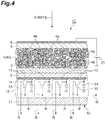
FIG. 4 , aradiation detector 1C is different from theradiation detector 1A in the configuration of theradiation absorption layer 4. In theradiation detector 1C, theradiation absorption layer 4 further containsinorganic semiconductor particles 4s, in addition to theperovskite structure particles 4p and thebinder resin 4r. Theinorganic semiconductor particles 4s are formed of an n-type semiconductor material. That is, a conductivity type of theinorganic semiconductor particle 4s is the same as the conductivity type of thedense layer 2 and theporous layer 3. As the n-type semiconductor material, an oxide such as titanium, silicon, zinc, niobium, tin, or aluminum, a sulfide thereof, a halide thereof, or the like is suitable. Theinorganic semiconductor particles 4s increase the mobility of the charge generated in theradiation absorption layer 4 due to the absorption of the X-rays. - Note that in the
radiation absorption layer 4 containing theperovskite structure particles 4p, electrons have higher mobility than holes. Therefore, it is preferable for an n-type semiconductor material to be selected as the material of theinorganic semiconductor particles 4s. Theinorganic semiconductor particles 4s formed of TiO2, SiO2, GeO2, or the like are particularly preferable from the viewpoint of increase of the mobility of the electrons. Theinorganic semiconductor particles 4s also function as nuclei for crystal growth of the perovskite material. - The method of manufacturing the
radiation detector 1C is the same as the method of manufacturing theradiation detector 1A described above except that theperovskite structure particles 4p and theinorganic semiconductor particles 4s are added to the solution in which thebinder resin 4r has been dissolved, and are completely dissolved to adjust the coating liquid containing theperovskite structure particles 4p, theinorganic semiconductor particles 4s, thebinder resin 4r, and the organic solvent. - That is, CH3NH2I and PbX2 are mixed in an organic solvent in a molar ratio of 1:1 to prepare methylammonium lead halide (here, CH3NH3PbX3) that is the
perovskite structure particle 4p. WhenPb X2 has completely reacted in the solution, the solution is distilled to obtain a perovskite structure crystal block formed of the methylammonium lead halide. The perovskite structure crystal block is pulverized to obtain theperovskite structure particle 4p. - Subsequently, the
binder resin 4r and the organic solvent are mixed and thebinder resin 4r is completely dissolved in the organic solvent. The organic solvent may be any organic solvent capable of dissolving thebinder resin 4r, may be formed of one type of solvent, or may be formed of two or more kinds of mixed solvents. Examples of thebinder resin 4r may include an acrylic organic resin, polyimide, polyvinyl alcohol, polyethylene, polyester, polycarbonate, or a polyurethane organic resin. Further, examples of the organic solvent include aromatics, ketones, alcohols, glycols, glycol ethers, and ethers. - Subsequently, the
perovskite structure particles 4p and theinorganic semiconductor particles 4s are added to the solution in which thebinder resin 4r has been dissolved, and are completely dissolved to adjust the coating liquid containing theperovskite structure particles 4p, theinorganic semiconductor particles 4s, thebinder resin 4r, and the organic solvent. - In the
radiation absorption layer 4, an average particle diameter of theperovskite structure particles 4p is larger than an average particle diameter of theinorganic semiconductor particles 4s. The average particle diameter of theinorganic semiconductor particles 4s is preferably 1 nm to 200 µm. However, when the average particle diameter of theinorganic semiconductor particles 4s is 10 nm or less, cohesion of theinorganic semiconductor particles 4s may occur and the dispersibility of theinorganic semiconductor particles 4s in theradiation absorption layer 4 may deteriorate. Therefore, the average particle diameter of theinorganic semiconductor particles 4s is more preferably 50 nm or more. Further, from the viewpoint of suppression of occurrence of crosstalk between the adjacentcharge collection electrodes 13, the average particle diameter of theinorganic semiconductor particles 4s is preferably 50% or less of a pixel pitch of the panel 10 (a distance between centers of the adjacent charge collection electrodes 13). A pulverizing method using a ball mill or a mortar, a sifting method, or the like can be appropriately used to obtain theinorganic semiconductor particles 4s having a desired average particle diameter. - When the average particle diameter of the
inorganic semiconductor particles 4s is larger than the average particle diameter of theperovskite structure particles 4p, a bulk density at the time of mixing decreases, which causes a decrease in the film density after drying. In order for theinorganic semiconductor particles 4s to fill gaps between theperovskite structure particles 4p and contribute to improvement of the bulk density, it is necessary for the average particle diameter of theinorganic semiconductor particles 4s to be smaller than the average particle diameter of theperovskite structure particles 4p. The average particle diameter of theinorganic semiconductor particles 4s is preferably 1/50 to 1/2 of the average particle diameter of theperovskite structure particles 4p. - The mixing amount of the
inorganic semiconductor particles 4s is preferably 70 wt% or less with respect to the mixing amount of theperovskite structure particles 4p. When the mixing amount of theinorganic semiconductor particles 4s increases, there is concern that a resistance value of theradiation absorption layer 4 may decrease and a dark current may increase, or a film density of theradiation absorption layer 4 may decrease and the absorption efficiency of the X-rays may decrease. Therefore, the mixing amount of theinorganic semiconductor particles 4s is more preferably 30 wt% or less with respect to the mixing amount of theperovskite structure particles 4p. On the other hand, when the mixing amount of theinorganic semiconductor particles 4s decreases, there is concern that an effect of the charge as a transporting material in theradiation absorption layer 4 may be degraded. Therefore, the mixing amount of theinorganic semiconductor particles 4s is more preferably 10 wt% or more with respect to the mixing amount of theperovskite structure particles 4p. - A ratio CB/CA of a film density CB of the
radiation absorption layer 4 to a density CA of theperovskite structure particle 4p is preferably 20 to 98%. From the viewpoint of improvement of a mobility of the charge generated due to the absorption of the X-rays and absorption efficiency of the X-rays, the ratio is more preferably 50% or more. However, when the mixing amount of theinorganic semiconductor particles 4s decreases, there is concern that an effect of the charge as a transporting material in theradiation absorption layer 4 may be degraded. Therefore, the ratio CB/CA is more preferably 95% or less. - According to the
radiation detector 1C described above, the same advantageous effects as those of theradiation detector 1A described above are achieved. - Further, in the
radiation detector 1C, theradiation absorption layer 4 further containsinorganic semiconductor particles 4s, in addition to theperovskite structure particles 4p and thebinder resin 4r. Accordingly, it is possible to increase the mobility of charge (electrons and holes) generated due to the absorption of the X-rays, and to obtain sufficient sensitivity and response characteristics. - It is necessary to thicken the
radiation absorption layer 4 in order to improve the absorption efficiency of the X-rays, but a distance to thecharge collection electrode 13 increases, and there is concern that charge collection efficiency may decrease. Theradiation absorption layer 4 containing theinorganic semiconductor particles 4s is particularly important in solving such a problem. - Further, in the
radiation detector 1C, the average particle diameter of theperovskite structure particles 4p is larger than the average particle diameter of theinorganic semiconductor particles 4s. Accordingly, it is possible to improve X-ray absorption efficiency and sensitivity. - Further, in the
radiation detector 1C, the conductivity type of theinorganic semiconductor particle 4s and the conductivity type of thedense layer 2 and theporous layer 3 are the same n type. Thus, the electrons generated in theradiation absorption layer 4 due to the absorption of the X-rays can be more smoothly moved to thecharge collection electrode 13. - Further, in the method of manufacturing the
radiation detector 1C, the perovskite structure crystal block is pulverized to obtain theperovskite structure particle 4p. Accordingly, since theperovskite structure particles 4p of which the particle diameter is reduced in a random state can be obtained, a filling rate of theperovskite structure particles 4p in theradiation absorption layer 4 increases. Thus, it is possible to obtain theradiation absorption layer 4 excellent in X-ray absorption efficiency and sensitivity. - The first embodiment, the second embodiment and the third embodiment of the present disclosure have been described above, but the present disclosure is not limited to each of the above-described embodiments. For example, each of the
radiation detectors radiation detectors dense layer 2. Each of theradiation detectors porous layer 3. Each of theradiation detectors hole transport layer 5. In each of theradiation detector porous layer 3 may be formed of an insulating material, such as AL2O3. - Further, the bias voltage may be applied to the
voltage application electrode 6 so that a positive potential difference is generated between thevoltage application electrode 6 and thecharge collection electrode 13. In this case, in theradiation detector 1A, it is preferable for thedense layer 2 and theporous layer 3 to be formed of a p-type semiconductor material (for example, copper oxide (Cu2O, CuO), nickel oxide (NiO), or cobalt oxide (CoO, Co3O4). In each of the radiation detectors IB and 1C, it is preferable for theinorganic semiconductor particles 4s among thedense layer 2, theporous layer 3, and theradiation absorption layer 4 to be formed of a p-type semiconductor material (for example, copper oxide (Cu2O, CuO), nickel oxide (NiO), or cobalt oxide (CoO, Co3O4). In each of theradiation detector charge collection electrode 13 collects the holes generated in theradiation absorption layer 4 due to the absorption of the X-rays. - 1A, 1B, 1C...radiation detector, 2...dense layer (semiconductor charge collection layer), 3...porous layer (semiconductor charge collection layer), 4...radiation absorption layer, 4p...perovskite structure particle, 4r...binder resin, 4s...inorganic semiconductor particle, 5...hole transport layer, 6...voltage application electrode, 10...panel (substrate), 13...charge collection electrode.
Claims (8)
- Aradiation detector (1A, 1B, 1C) comprising:a substrate (11) including a charge collection electrode (13);a radiation absorption layer (4) disposed on one side with respect to the substrate (11); anda voltage application electrode (6) disposed on the one side with respect to the radiation absorption layer (4), a bias voltage being applied to the voltage application electrode so that a potential difference is generated between the voltage application electrode (6) and the charge collection electrode (13),characterized by the radiation absorption layer (4) including perovskite structure particles (4p) and a binder resin (4r).
- The radiation detector (1B, 1C) according to claim 1, wherein the radiation absorption layer (4) further includes inorganic semiconductor particles (4s) other than the perovskite structure particles (4p).
- The radiation detector (1B, 1C) according to claim 2, wherein an average particle diameter of the perovskite structure particles (4p) is larger than an average particle diameter of the inorganic semiconductor particles (4s).
- The radiation detector (1B, 1C) according to claim 2 or 3, further comprising a semiconductor charge collection layer (3) disposed between the substrate (11) and the radiation absorption layer (4).
- The radiation detector (1B, 1C) according to claim 4, wherein a conductivity type of the inorganic semiconductor particles (4s) and a conductivity type of the semiconductor charge collection layer (3) are the same.
- The radiation detector (1A, 1B, 1C) according to any one of claims 1 to 5, further comprising a hole transport layer (5) disposed between the radiation absorption layer (4) and the voltage application electrode (6).
- A method of manufacturing a radiation detector (1A, 1B, 1C), the method comprising:a first step of preparing a coating solution containing perovskite structure particles (4p), a binder resin (4r), and an organic solvent;a second step of forming a radiation absorption layer (4) on one side with respect to a substrate (11) including a charge collection electrode (13) through screen printing using the coating solution after the first step, the radiation absorption layer (4) containing the perovskite structure particles (4p) and the binder resin (4r); anda third step of forming a voltage application electrode (6) on the one side with respect to the radiation absorption layer (4) after the second step, a bias voltage being applied to the voltage application electrode (6) such that a potential difference is generated between the voltage application electrode (6) and the charge collection electrode (13) .
- The method according to claim 7, further comprising a step of pulverizing a perovskite structure crystal block to obtain the perovskite structure particles (4p) before the first step.
Applications Claiming Priority (2)
| Application Number | Priority Date | Filing Date | Title |
|---|---|---|---|
| JP2015219211A JP6535271B2 (en) | 2015-11-09 | 2015-11-09 | Radiation detector and method of manufacturing radiation detector |
| PCT/JP2016/082051 WO2017082081A1 (en) | 2015-11-09 | 2016-10-28 | Radiation detector and manufacturing method for radiation detector |
Publications (3)
| Publication Number | Publication Date |
|---|---|
| EP3376260A1 EP3376260A1 (en) | 2018-09-19 |
| EP3376260A4 EP3376260A4 (en) | 2019-07-17 |
| EP3376260B1 true EP3376260B1 (en) | 2020-06-03 |
Family
ID=58696117
Family Applications (1)
| Application Number | Title | Priority Date | Filing Date |
|---|---|---|---|
| EP16864044.9A Active EP3376260B1 (en) | 2015-11-09 | 2016-10-28 | Radiation detector and manufacturing method for radiation detector |
Country Status (6)
| Country | Link |
|---|---|
| US (1) | US10816681B2 (en) |
| EP (1) | EP3376260B1 (en) |
| JP (1) | JP6535271B2 (en) |
| KR (1) | KR102480425B1 (en) |
| CN (1) | CN108351428B (en) |
| WO (1) | WO2017082081A1 (en) |
Families Citing this family (15)
| Publication number | Priority date | Publication date | Assignee | Title |
|---|---|---|---|---|
| CN109285846B (en) * | 2017-07-20 | 2023-10-13 | 松下知识产权经营株式会社 | Photosensor and photodetector using the same |
| EP3474339A1 (en) | 2017-10-20 | 2019-04-24 | Siemens Healthcare GmbH | X-ray image sensor with adhesion promotive interlayer and soft-sintered perovskite active layer |
| CN108318907B (en) * | 2018-02-01 | 2019-10-01 | 北京京东方光电科技有限公司 | X-ray detection panel and its manufacturing method and X-ray detection device |
| CN112313543A (en) | 2018-06-26 | 2021-02-02 | 国立大学法人京都大学 | Radiation detector and method for manufacturing radiation detector |
| CN109206449B (en) * | 2018-08-01 | 2020-05-15 | 南京航空航天大学 | Organic-inorganic perovskite crystal material and preparation method and application thereof |
| EP3863054A1 (en) | 2020-02-04 | 2021-08-11 | Siemens Healthcare GmbH | Multiple spectral detectors using structured perovskite |
| EP3863059A1 (en) | 2020-02-04 | 2021-08-11 | Siemens Healthcare GmbH | Perovskite detectors with enhanced adhesion |
| CN111286252A (en) * | 2020-03-09 | 2020-06-16 | 长沙而道新能源科技有限公司 | Radiation-resistant anticorrosive paint and preparation method thereof |
| EP3916819A1 (en) * | 2020-05-29 | 2021-12-01 | Nederlandse Organisatie voor toegepast- natuurwetenschappelijk Onderzoek TNO | Perovskite layer |
| JP2023127003A (en) * | 2020-08-06 | 2023-09-13 | パナソニックIpマネジメント株式会社 | Ionizing radiation conversion device and ionizing radiation detection method |
| KR102474979B1 (en) * | 2021-01-12 | 2022-12-06 | 주식회사 파프리카랩 | System for monitoring radiation exposure using appararus of skin attachment type for measuring radiation |
| CN113035900B (en) * | 2021-02-26 | 2023-02-10 | 深圳先进技术研究院 | Direct electromagnetic radiation detector and preparation method thereof |
| EP4068363B1 (en) | 2021-03-30 | 2023-06-07 | Siemens Healthcare GmbH | Radiation detector with butted absorber tiles without dead areas |
| CN113970779A (en) * | 2021-10-12 | 2022-01-25 | 华北电力大学 | Microstructure scintillation screen formed by perovskite filled microporous panel and preparation method |
| EP4180845A1 (en) | 2021-11-11 | 2023-05-17 | Siemens Healthcare GmbH | Radiation detector with laser cut absorber tiles |
Family Cites Families (14)
| Publication number | Priority date | Publication date | Assignee | Title |
|---|---|---|---|---|
| JP3669860B2 (en) * | 1999-03-10 | 2005-07-13 | Tdk株式会社 | Laminated thin film |
| JP3779604B2 (en) | 2001-01-15 | 2006-05-31 | 独立行政法人科学技術振興機構 | Radiation detector |
| JP3714918B2 (en) | 2001-07-31 | 2005-11-09 | 独立行政法人科学技術振興機構 | Radiation detector |
| JP4269859B2 (en) * | 2003-09-10 | 2009-05-27 | 株式会社島津製作所 | Radiation detector |
| CN102888652B (en) * | 2004-11-08 | 2016-09-21 | 东北泰克诺亚奇股份有限公司 | Single crystal for scintillator containing Pr and manufacture method and radiation detector and check device |
| WO2006068130A1 (en) * | 2004-12-21 | 2006-06-29 | Hitachi Metals, Ltd. | Fluorescent material and method for preparation thereof, radiation detector using fluorescent material, and x-ray ct device |
| WO2007096967A1 (en) * | 2006-02-23 | 2007-08-30 | Shimadzu Corporation | Radiation detector |
| JP2008039548A (en) * | 2006-08-04 | 2008-02-21 | Ohyo Koken Kogyo Co Ltd | Scintillation detector |
| JP5521412B2 (en) * | 2008-07-31 | 2014-06-11 | 日立金属株式会社 | Fluorescent material, scintillator and radiation detector using the same |
| JP2011054638A (en) * | 2009-08-31 | 2011-03-17 | Fujifilm Corp | Method of manufacturing photoconductive layer |
| JP6066608B2 (en) | 2011-07-27 | 2017-01-25 | キヤノン株式会社 | Scintillator having phase separation structure and radiation detector using the same |
| US9812660B2 (en) * | 2013-12-19 | 2017-11-07 | Nutech Ventures | Method for single crystal growth of photovoltaic perovskite material and devices |
| DE102015225145A1 (en) * | 2015-12-14 | 2017-06-14 | Siemens Healthcare Gmbh | Perovskite particles for the preparation of X-ray detectors by means of dry-phase deposition |
| DE102016205818A1 (en) * | 2016-04-07 | 2017-10-12 | Siemens Healthcare Gmbh | Apparatus and method for detecting X-radiation |
-
2015
- 2015-11-09 JP JP2015219211A patent/JP6535271B2/en active Active
-
2016
- 2016-10-28 CN CN201680065192.1A patent/CN108351428B/en active Active
- 2016-10-28 EP EP16864044.9A patent/EP3376260B1/en active Active
- 2016-10-28 WO PCT/JP2016/082051 patent/WO2017082081A1/en active Application Filing
- 2016-10-28 US US15/773,618 patent/US10816681B2/en active Active
- 2016-10-28 KR KR1020187014557A patent/KR102480425B1/en active IP Right Grant
Non-Patent Citations (1)
| Title |
|---|
| None * |
Also Published As
| Publication number | Publication date |
|---|---|
| EP3376260A4 (en) | 2019-07-17 |
| JP2017090186A (en) | 2017-05-25 |
| CN108351428B (en) | 2021-08-17 |
| US10816681B2 (en) | 2020-10-27 |
| EP3376260A1 (en) | 2018-09-19 |
| WO2017082081A1 (en) | 2017-05-18 |
| KR102480425B1 (en) | 2022-12-23 |
| CN108351428A (en) | 2018-07-31 |
| US20200257006A1 (en) | 2020-08-13 |
| KR20180081742A (en) | 2018-07-17 |
| JP6535271B2 (en) | 2019-06-26 |
Similar Documents
| Publication | Publication Date | Title |
|---|---|---|
| EP3376260B1 (en) | Radiation detector and manufacturing method for radiation detector | |
| KR101819757B1 (en) | Photodiode and other sensor structures in flat-panel x-ray imagers and method for improving topological uniformity of the photodiode and other sensor structures in flat-panel x-ray imagers based on thin-film electronics | |
| US7902512B1 (en) | Coplanar high fill factor pixel architecture | |
| US8791419B2 (en) | High charge capacity pixel architecture, photoelectric conversion apparatus, radiation image pickup system and methods for same | |
| JP4547760B2 (en) | Radiation detector and radiation imaging apparatus | |
| US7122803B2 (en) | Amorphous selenium flat panel x-ray imager for tomosynthesis and static imaging | |
| CA2669678C (en) | Photodetector/imaging device with avalanche gain | |
| US7233005B2 (en) | Amorphous selenium flat panel x-ray imager for tomosynthesis and static imaging | |
| US8735839B2 (en) | Pastes for photoelectric conversion layers of X-ray detectors, X-ray detectors and methods of manufacturing the same | |
| US8129810B2 (en) | Continuous large area imaging and display arrays using readout arrays fabricated in silicon-on-glass substrates | |
| CN109585477B (en) | Flat panel detector structure and preparation method thereof | |
| WO2015186657A1 (en) | Semiconductor device and method for manufacturing same | |
| US20180329080A1 (en) | Detector element for detecting incident x-ray radiation | |
| US7632539B2 (en) | Method for manufacturing photoconductive layers that constitute radiation imaging panels | |
| US8232531B2 (en) | Corrosion barrier layer for photoconductive X-ray imagers | |
| JP2019506733A (en) | Optoelectronic array device with upper transparent electrode | |
| US9348037B2 (en) | X-ray pixels including double photoconductors and X-ray detectors including the X-ray pixels | |
| WO2016130978A1 (en) | Radiation detector | |
| CN112928137B (en) | Organic photoelectric flat panel detector | |
| Shrestha et al. | A perspective on the device physics of lead halide perovskite semiconducting detector for gamma and x-ray sensing | |
| WO2013065212A1 (en) | Radiation detector | |
| KR101829992B1 (en) | X-ray detector having photoconductor comprising perovskite compound | |
| CN112736201A (en) | Indirect flat panel detector and preparation method thereof |
Legal Events
| Date | Code | Title | Description |
|---|---|---|---|
| STAA | Information on the status of an ep patent application or granted ep patent |
Free format text: STATUS: THE INTERNATIONAL PUBLICATION HAS BEEN MADE |
|
| PUAI | Public reference made under article 153(3) epc to a published international application that has entered the european phase |
Free format text: ORIGINAL CODE: 0009012 |
|
| STAA | Information on the status of an ep patent application or granted ep patent |
Free format text: STATUS: REQUEST FOR EXAMINATION WAS MADE |
|
| 17P | Request for examination filed |
Effective date: 20180509 |
|
| AK | Designated contracting states |
Kind code of ref document: A1 Designated state(s): AL AT BE BG CH CY CZ DE DK EE ES FI FR GB GR HR HU IE IS IT LI LT LU LV MC MK MT NL NO PL PT RO RS SE SI SK SM TR |
|
| AX | Request for extension of the european patent |
Extension state: BA ME |
|
| DAV | Request for validation of the european patent (deleted) | ||
| DAX | Request for extension of the european patent (deleted) | ||
| A4 | Supplementary search report drawn up and despatched |
Effective date: 20190618 |
|
| RIC1 | Information provided on ipc code assigned before grant |
Ipc: H01L 27/30 20060101ALI20190612BHEP Ipc: H01L 27/144 20060101AFI20190612BHEP Ipc: H01L 27/146 20060101ALI20190612BHEP Ipc: H01L 51/42 20060101ALI20190612BHEP |
|
| REG | Reference to a national code |
Ref country code: DE Ref legal event code: R079 Ref document number: 602016037702 Country of ref document: DE Free format text: PREVIOUS MAIN CLASS: G01T0001240000 Ipc: H01L0027300000 |
|
| GRAP | Despatch of communication of intention to grant a patent |
Free format text: ORIGINAL CODE: EPIDOSNIGR1 |
|
| STAA | Information on the status of an ep patent application or granted ep patent |
Free format text: STATUS: GRANT OF PATENT IS INTENDED |
|
| RIC1 | Information provided on ipc code assigned before grant |
Ipc: H01L 27/30 20060101AFI20191118BHEP Ipc: H01L 51/42 20060101ALI20191118BHEP |
|
| INTG | Intention to grant announced |
Effective date: 20191204 |
|
| RIN1 | Information on inventor provided before grant (corrected) |
Inventor name: IZAWA, TOSHIYUKI Inventor name: YAMAMOTO, KOEI Inventor name: ABE, KEIJI |
|
| GRAS | Grant fee paid |
Free format text: ORIGINAL CODE: EPIDOSNIGR3 |
|
| GRAJ | Information related to disapproval of communication of intention to grant by the applicant or resumption of examination proceedings by the epo deleted |
Free format text: ORIGINAL CODE: EPIDOSDIGR1 |
|
| GRAL | Information related to payment of fee for publishing/printing deleted |
Free format text: ORIGINAL CODE: EPIDOSDIGR3 |
|
| STAA | Information on the status of an ep patent application or granted ep patent |
Free format text: STATUS: REQUEST FOR EXAMINATION WAS MADE |
|
| INTC | Intention to grant announced (deleted) | ||
| GRAJ | Information related to disapproval of communication of intention to grant by the applicant or resumption of examination proceedings by the epo deleted |
Free format text: ORIGINAL CODE: EPIDOSDIGR1 |
|
| GRAP | Despatch of communication of intention to grant a patent |
Free format text: ORIGINAL CODE: EPIDOSNIGR1 |
|
| GRAJ | Information related to disapproval of communication of intention to grant by the applicant or resumption of examination proceedings by the epo deleted |
Free format text: ORIGINAL CODE: EPIDOSDIGR1 |
|
| GRAR | Information related to intention to grant a patent recorded |
Free format text: ORIGINAL CODE: EPIDOSNIGR71 |
|
| STAA | Information on the status of an ep patent application or granted ep patent |
Free format text: STATUS: GRANT OF PATENT IS INTENDED |
|
| GRAA | (expected) grant |
Free format text: ORIGINAL CODE: 0009210 |
|
| STAA | Information on the status of an ep patent application or granted ep patent |
Free format text: STATUS: THE PATENT HAS BEEN GRANTED |
|
| INTG | Intention to grant announced |
Effective date: 20200422 |
|
| AK | Designated contracting states |
Kind code of ref document: B1 Designated state(s): AL AT BE BG CH CY CZ DE DK EE ES FI FR GB GR HR HU IE IS IT LI LT LU LV MC MK MT NL NO PL PT RO RS SE SI SK SM TR |
|
| REG | Reference to a national code |
Ref country code: GB Ref legal event code: FG4D |
|
| REG | Reference to a national code |
Ref country code: CH Ref legal event code: EP Ref country code: AT Ref legal event code: REF Ref document number: 1277919 Country of ref document: AT Kind code of ref document: T Effective date: 20200615 |
|
| REG | Reference to a national code |
Ref country code: DE Ref legal event code: R096 Ref document number: 602016037702 Country of ref document: DE |
|
| REG | Reference to a national code |
Ref country code: FI Ref legal event code: FGE |
|
| REG | Reference to a national code |
Ref country code: LT Ref legal event code: MG4D |
|
| PG25 | Lapsed in a contracting state [announced via postgrant information from national office to epo] |
Ref country code: SE Free format text: LAPSE BECAUSE OF FAILURE TO SUBMIT A TRANSLATION OF THE DESCRIPTION OR TO PAY THE FEE WITHIN THE PRESCRIBED TIME-LIMIT Effective date: 20200603 Ref country code: NO Free format text: LAPSE BECAUSE OF FAILURE TO SUBMIT A TRANSLATION OF THE DESCRIPTION OR TO PAY THE FEE WITHIN THE PRESCRIBED TIME-LIMIT Effective date: 20200903 Ref country code: LT Free format text: LAPSE BECAUSE OF FAILURE TO SUBMIT A TRANSLATION OF THE DESCRIPTION OR TO PAY THE FEE WITHIN THE PRESCRIBED TIME-LIMIT Effective date: 20200603 Ref country code: GR Free format text: LAPSE BECAUSE OF FAILURE TO SUBMIT A TRANSLATION OF THE DESCRIPTION OR TO PAY THE FEE WITHIN THE PRESCRIBED TIME-LIMIT Effective date: 20200904 |
|
| REG | Reference to a national code |
Ref country code: NL Ref legal event code: MP Effective date: 20200603 |
|
| PG25 | Lapsed in a contracting state [announced via postgrant information from national office to epo] |
Ref country code: BG Free format text: LAPSE BECAUSE OF FAILURE TO SUBMIT A TRANSLATION OF THE DESCRIPTION OR TO PAY THE FEE WITHIN THE PRESCRIBED TIME-LIMIT Effective date: 20200903 Ref country code: RS Free format text: LAPSE BECAUSE OF FAILURE TO SUBMIT A TRANSLATION OF THE DESCRIPTION OR TO PAY THE FEE WITHIN THE PRESCRIBED TIME-LIMIT Effective date: 20200603 Ref country code: LV Free format text: LAPSE BECAUSE OF FAILURE TO SUBMIT A TRANSLATION OF THE DESCRIPTION OR TO PAY THE FEE WITHIN THE PRESCRIBED TIME-LIMIT Effective date: 20200603 Ref country code: HR Free format text: LAPSE BECAUSE OF FAILURE TO SUBMIT A TRANSLATION OF THE DESCRIPTION OR TO PAY THE FEE WITHIN THE PRESCRIBED TIME-LIMIT Effective date: 20200603 |
|
| REG | Reference to a national code |
Ref country code: AT Ref legal event code: MK05 Ref document number: 1277919 Country of ref document: AT Kind code of ref document: T Effective date: 20200603 |
|
| PG25 | Lapsed in a contracting state [announced via postgrant information from national office to epo] |
Ref country code: AL Free format text: LAPSE BECAUSE OF FAILURE TO SUBMIT A TRANSLATION OF THE DESCRIPTION OR TO PAY THE FEE WITHIN THE PRESCRIBED TIME-LIMIT Effective date: 20200603 Ref country code: NL Free format text: LAPSE BECAUSE OF FAILURE TO SUBMIT A TRANSLATION OF THE DESCRIPTION OR TO PAY THE FEE WITHIN THE PRESCRIBED TIME-LIMIT Effective date: 20200603 |
|
| PG25 | Lapsed in a contracting state [announced via postgrant information from national office to epo] |
Ref country code: EE Free format text: LAPSE BECAUSE OF FAILURE TO SUBMIT A TRANSLATION OF THE DESCRIPTION OR TO PAY THE FEE WITHIN THE PRESCRIBED TIME-LIMIT Effective date: 20200603 Ref country code: SM Free format text: LAPSE BECAUSE OF FAILURE TO SUBMIT A TRANSLATION OF THE DESCRIPTION OR TO PAY THE FEE WITHIN THE PRESCRIBED TIME-LIMIT Effective date: 20200603 Ref country code: AT Free format text: LAPSE BECAUSE OF FAILURE TO SUBMIT A TRANSLATION OF THE DESCRIPTION OR TO PAY THE FEE WITHIN THE PRESCRIBED TIME-LIMIT Effective date: 20200603 Ref country code: IT Free format text: LAPSE BECAUSE OF FAILURE TO SUBMIT A TRANSLATION OF THE DESCRIPTION OR TO PAY THE FEE WITHIN THE PRESCRIBED TIME-LIMIT Effective date: 20200603 Ref country code: PT Free format text: LAPSE BECAUSE OF FAILURE TO SUBMIT A TRANSLATION OF THE DESCRIPTION OR TO PAY THE FEE WITHIN THE PRESCRIBED TIME-LIMIT Effective date: 20201006 Ref country code: RO Free format text: LAPSE BECAUSE OF FAILURE TO SUBMIT A TRANSLATION OF THE DESCRIPTION OR TO PAY THE FEE WITHIN THE PRESCRIBED TIME-LIMIT Effective date: 20200603 Ref country code: CZ Free format text: LAPSE BECAUSE OF FAILURE TO SUBMIT A TRANSLATION OF THE DESCRIPTION OR TO PAY THE FEE WITHIN THE PRESCRIBED TIME-LIMIT Effective date: 20200603 Ref country code: ES Free format text: LAPSE BECAUSE OF FAILURE TO SUBMIT A TRANSLATION OF THE DESCRIPTION OR TO PAY THE FEE WITHIN THE PRESCRIBED TIME-LIMIT Effective date: 20200603 |
|
| PG25 | Lapsed in a contracting state [announced via postgrant information from national office to epo] |
Ref country code: PL Free format text: LAPSE BECAUSE OF FAILURE TO SUBMIT A TRANSLATION OF THE DESCRIPTION OR TO PAY THE FEE WITHIN THE PRESCRIBED TIME-LIMIT Effective date: 20200603 Ref country code: SK Free format text: LAPSE BECAUSE OF FAILURE TO SUBMIT A TRANSLATION OF THE DESCRIPTION OR TO PAY THE FEE WITHIN THE PRESCRIBED TIME-LIMIT Effective date: 20200603 Ref country code: IS Free format text: LAPSE BECAUSE OF FAILURE TO SUBMIT A TRANSLATION OF THE DESCRIPTION OR TO PAY THE FEE WITHIN THE PRESCRIBED TIME-LIMIT Effective date: 20201003 |
|
| REG | Reference to a national code |
Ref country code: DE Ref legal event code: R097 Ref document number: 602016037702 Country of ref document: DE |
|
| PLBE | No opposition filed within time limit |
Free format text: ORIGINAL CODE: 0009261 |
|
| STAA | Information on the status of an ep patent application or granted ep patent |
Free format text: STATUS: NO OPPOSITION FILED WITHIN TIME LIMIT |
|
| PG25 | Lapsed in a contracting state [announced via postgrant information from national office to epo] |
Ref country code: DK Free format text: LAPSE BECAUSE OF FAILURE TO SUBMIT A TRANSLATION OF THE DESCRIPTION OR TO PAY THE FEE WITHIN THE PRESCRIBED TIME-LIMIT Effective date: 20200603 |
|
| 26N | No opposition filed |
Effective date: 20210304 |
|
| PG25 | Lapsed in a contracting state [announced via postgrant information from national office to epo] |
Ref country code: SI Free format text: LAPSE BECAUSE OF FAILURE TO SUBMIT A TRANSLATION OF THE DESCRIPTION OR TO PAY THE FEE WITHIN THE PRESCRIBED TIME-LIMIT Effective date: 20200603 |
|
| REG | Reference to a national code |
Ref country code: CH Ref legal event code: PL |
|
| PG25 | Lapsed in a contracting state [announced via postgrant information from national office to epo] |
Ref country code: LU Free format text: LAPSE BECAUSE OF NON-PAYMENT OF DUE FEES Effective date: 20201028 Ref country code: MC Free format text: LAPSE BECAUSE OF FAILURE TO SUBMIT A TRANSLATION OF THE DESCRIPTION OR TO PAY THE FEE WITHIN THE PRESCRIBED TIME-LIMIT Effective date: 20200603 |
|
| REG | Reference to a national code |
Ref country code: BE Ref legal event code: MM Effective date: 20201031 |
|
| PG25 | Lapsed in a contracting state [announced via postgrant information from national office to epo] |
Ref country code: CH Free format text: LAPSE BECAUSE OF NON-PAYMENT OF DUE FEES Effective date: 20201031 Ref country code: BE Free format text: LAPSE BECAUSE OF NON-PAYMENT OF DUE FEES Effective date: 20201031 Ref country code: LI Free format text: LAPSE BECAUSE OF NON-PAYMENT OF DUE FEES Effective date: 20201031 |
|
| PG25 | Lapsed in a contracting state [announced via postgrant information from national office to epo] |
Ref country code: IE Free format text: LAPSE BECAUSE OF NON-PAYMENT OF DUE FEES Effective date: 20201028 |
|
| PG25 | Lapsed in a contracting state [announced via postgrant information from national office to epo] |
Ref country code: TR Free format text: LAPSE BECAUSE OF FAILURE TO SUBMIT A TRANSLATION OF THE DESCRIPTION OR TO PAY THE FEE WITHIN THE PRESCRIBED TIME-LIMIT Effective date: 20200603 Ref country code: MT Free format text: LAPSE BECAUSE OF FAILURE TO SUBMIT A TRANSLATION OF THE DESCRIPTION OR TO PAY THE FEE WITHIN THE PRESCRIBED TIME-LIMIT Effective date: 20200603 Ref country code: CY Free format text: LAPSE BECAUSE OF FAILURE TO SUBMIT A TRANSLATION OF THE DESCRIPTION OR TO PAY THE FEE WITHIN THE PRESCRIBED TIME-LIMIT Effective date: 20200603 |
|
| PG25 | Lapsed in a contracting state [announced via postgrant information from national office to epo] |
Ref country code: MK Free format text: LAPSE BECAUSE OF FAILURE TO SUBMIT A TRANSLATION OF THE DESCRIPTION OR TO PAY THE FEE WITHIN THE PRESCRIBED TIME-LIMIT Effective date: 20200603 |
|
| REG | Reference to a national code |
Ref country code: DE Ref legal event code: R079 Ref document number: 602016037702 Country of ref document: DE Free format text: PREVIOUS MAIN CLASS: H01L0027300000 Ipc: H10K0039000000 |
|
| P01 | Opt-out of the competence of the unified patent court (upc) registered |
Effective date: 20230509 |
|
| PGFP | Annual fee paid to national office [announced via postgrant information from national office to epo] |
Ref country code: GB Payment date: 20230907 Year of fee payment: 8 |
|
| PGFP | Annual fee paid to national office [announced via postgrant information from national office to epo] |
Ref country code: FR Payment date: 20230911 Year of fee payment: 8 |
|
| PGFP | Annual fee paid to national office [announced via postgrant information from national office to epo] |
Ref country code: FI Payment date: 20231011 Year of fee payment: 8 Ref country code: DE Payment date: 20230906 Year of fee payment: 8 |