EP3344972B1 - Optische systeme und verfahren zur charakterisierung von high-k-dielektrika - Google Patents
Optische systeme und verfahren zur charakterisierung von high-k-dielektrika Download PDFInfo
- Publication number
- EP3344972B1 EP3344972B1 EP16843152.6A EP16843152A EP3344972B1 EP 3344972 B1 EP3344972 B1 EP 3344972B1 EP 16843152 A EP16843152 A EP 16843152A EP 3344972 B1 EP3344972 B1 EP 3344972B1
- Authority
- EP
- European Patent Office
- Prior art keywords
- region
- time constant
- dielectric layer
- semiconductor
- spectrum
- Prior art date
- Legal status (The legal status is an assumption and is not a legal conclusion. Google has not performed a legal analysis and makes no representation as to the accuracy of the status listed.)
- Active
Links
Images


Classifications
-
- G—PHYSICS
- G01—MEASURING; TESTING
- G01N—INVESTIGATING OR ANALYSING MATERIALS BY DETERMINING THEIR CHEMICAL OR PHYSICAL PROPERTIES
- G01N21/00—Investigating or analysing materials by the use of optical means, i.e. using sub-millimetre waves, infrared, visible or ultraviolet light
- G01N21/62—Systems in which the material investigated is excited whereby it emits light or causes a change in wavelength of the incident light
- G01N21/63—Systems in which the material investigated is excited whereby it emits light or causes a change in wavelength of the incident light optically excited
- G01N21/636—Systems in which the material investigated is excited whereby it emits light or causes a change in wavelength of the incident light optically excited using an arrangement of pump beam and probe beam; using the measurement of optical non-linear properties
-
- G—PHYSICS
- G01—MEASURING; TESTING
- G01N—INVESTIGATING OR ANALYSING MATERIALS BY DETERMINING THEIR CHEMICAL OR PHYSICAL PROPERTIES
- G01N21/00—Investigating or analysing materials by the use of optical means, i.e. using sub-millimetre waves, infrared, visible or ultraviolet light
- G01N21/17—Systems in which incident light is modified in accordance with the properties of the material investigated
- G01N21/25—Colour; Spectral properties, i.e. comparison of effect of material on the light at two or more different wavelengths or wavelength bands
- G01N21/256—Arrangements using two alternating lights and one detector
-
- G—PHYSICS
- G01—MEASURING; TESTING
- G01N—INVESTIGATING OR ANALYSING MATERIALS BY DETERMINING THEIR CHEMICAL OR PHYSICAL PROPERTIES
- G01N21/00—Investigating or analysing materials by the use of optical means, i.e. using sub-millimetre waves, infrared, visible or ultraviolet light
- G01N21/17—Systems in which incident light is modified in accordance with the properties of the material investigated
- G01N21/25—Colour; Spectral properties, i.e. comparison of effect of material on the light at two or more different wavelengths or wavelength bands
- G01N21/27—Colour; Spectral properties, i.e. comparison of effect of material on the light at two or more different wavelengths or wavelength bands using photo-electric detection ; circuits for computing concentration
- G01N21/272—Colour; Spectral properties, i.e. comparison of effect of material on the light at two or more different wavelengths or wavelength bands using photo-electric detection ; circuits for computing concentration for following a reaction, e.g. for determining photometrically a reaction rate (photometric cinetic analysis)
-
- G—PHYSICS
- G01—MEASURING; TESTING
- G01N—INVESTIGATING OR ANALYSING MATERIALS BY DETERMINING THEIR CHEMICAL OR PHYSICAL PROPERTIES
- G01N21/00—Investigating or analysing materials by the use of optical means, i.e. using sub-millimetre waves, infrared, visible or ultraviolet light
- G01N21/62—Systems in which the material investigated is excited whereby it emits light or causes a change in wavelength of the incident light
- G01N21/63—Systems in which the material investigated is excited whereby it emits light or causes a change in wavelength of the incident light optically excited
- G01N21/64—Fluorescence; Phosphorescence
- G01N21/6489—Photoluminescence of semiconductors
-
- G—PHYSICS
- G01—MEASURING; TESTING
- G01N—INVESTIGATING OR ANALYSING MATERIALS BY DETERMINING THEIR CHEMICAL OR PHYSICAL PROPERTIES
- G01N21/00—Investigating or analysing materials by the use of optical means, i.e. using sub-millimetre waves, infrared, visible or ultraviolet light
- G01N21/84—Systems specially adapted for particular applications
- G01N21/88—Investigating the presence of flaws or contamination
- G01N21/8851—Scan or image signal processing specially adapted therefor, e.g. for scan signal adjustment, for detecting different kinds of defects, for compensating for structures, markings, edges
-
- G—PHYSICS
- G01—MEASURING; TESTING
- G01N—INVESTIGATING OR ANALYSING MATERIALS BY DETERMINING THEIR CHEMICAL OR PHYSICAL PROPERTIES
- G01N21/00—Investigating or analysing materials by the use of optical means, i.e. using sub-millimetre waves, infrared, visible or ultraviolet light
- G01N21/84—Systems specially adapted for particular applications
- G01N21/88—Investigating the presence of flaws or contamination
- G01N21/95—Investigating the presence of flaws or contamination characterised by the material or shape of the object to be examined
- G01N21/9501—Semiconductor wafers
- G01N21/9505—Wafer internal defects, e.g. microcracks
-
- G—PHYSICS
- G01—MEASURING; TESTING
- G01R—MEASURING ELECTRIC VARIABLES; MEASURING MAGNETIC VARIABLES
- G01R29/00—Arrangements for measuring or indicating electric quantities not covered by groups G01R19/00 - G01R27/00
- G01R29/24—Arrangements for measuring quantities of charge
-
- G—PHYSICS
- G01—MEASURING; TESTING
- G01R—MEASURING ELECTRIC VARIABLES; MEASURING MAGNETIC VARIABLES
- G01R31/00—Arrangements for testing electric properties; Arrangements for locating electric faults; Arrangements for electrical testing characterised by what is being tested not provided for elsewhere
- G01R31/26—Testing of individual semiconductor devices
- G01R31/2648—Characterising semiconductor materials
-
- G—PHYSICS
- G01—MEASURING; TESTING
- G01R—MEASURING ELECTRIC VARIABLES; MEASURING MAGNETIC VARIABLES
- G01R31/00—Arrangements for testing electric properties; Arrangements for locating electric faults; Arrangements for electrical testing characterised by what is being tested not provided for elsewhere
- G01R31/28—Testing of electronic circuits, e.g. by signal tracer
- G01R31/302—Contactless testing
-
- H—ELECTRICITY
- H10—SEMICONDUCTOR DEVICES; ELECTRIC SOLID-STATE DEVICES NOT OTHERWISE PROVIDED FOR
- H10D—INORGANIC ELECTRIC SEMICONDUCTOR DEVICES
- H10D64/00—Electrodes of devices having potential barriers
- H10D64/118—Electrodes comprising insulating layers having particular dielectric or electrostatic properties, e.g. having static charges
-
- H10P74/203—
-
- G—PHYSICS
- G01—MEASURING; TESTING
- G01N—INVESTIGATING OR ANALYSING MATERIALS BY DETERMINING THEIR CHEMICAL OR PHYSICAL PROPERTIES
- G01N21/00—Investigating or analysing materials by the use of optical means, i.e. using sub-millimetre waves, infrared, visible or ultraviolet light
- G01N21/17—Systems in which incident light is modified in accordance with the properties of the material investigated
- G01N21/25—Colour; Spectral properties, i.e. comparison of effect of material on the light at two or more different wavelengths or wavelength bands
- G01N2021/258—Surface plasmon spectroscopy, e.g. micro- or nanoparticles in suspension
-
- G—PHYSICS
- G01—MEASURING; TESTING
- G01N—INVESTIGATING OR ANALYSING MATERIALS BY DETERMINING THEIR CHEMICAL OR PHYSICAL PROPERTIES
- G01N21/00—Investigating or analysing materials by the use of optical means, i.e. using sub-millimetre waves, infrared, visible or ultraviolet light
- G01N21/84—Systems specially adapted for particular applications
- G01N21/88—Investigating the presence of flaws or contamination
- G01N21/95—Investigating the presence of flaws or contamination characterised by the material or shape of the object to be examined
- G01N21/9501—Semiconductor wafers
-
- G—PHYSICS
- G01—MEASURING; TESTING
- G01R—MEASURING ELECTRIC VARIABLES; MEASURING MAGNETIC VARIABLES
- G01R31/00—Arrangements for testing electric properties; Arrangements for locating electric faults; Arrangements for electrical testing characterised by what is being tested not provided for elsewhere
- G01R31/26—Testing of individual semiconductor devices
- G01R31/265—Contactless testing
- G01R31/2656—Contactless testing using non-ionising electromagnetic radiation, e.g. optical radiation
-
- H—ELECTRICITY
- H10—SEMICONDUCTOR DEVICES; ELECTRIC SOLID-STATE DEVICES NOT OTHERWISE PROVIDED FOR
- H10D—INORGANIC ELECTRIC SEMICONDUCTOR DEVICES
- H10D64/00—Electrodes of devices having potential barriers
- H10D64/20—Electrodes characterised by their shapes, relative sizes or dispositions
- H10D64/27—Electrodes not carrying the current to be rectified, amplified, oscillated or switched, e.g. gates
- H10D64/311—Gate electrodes for field-effect devices
- H10D64/411—Gate electrodes for field-effect devices for FETs
- H10D64/511—Gate electrodes for field-effect devices for FETs for IGFETs
- H10D64/514—Gate electrodes for field-effect devices for FETs for IGFETs characterised by the insulating layers
-
- H—ELECTRICITY
- H10—SEMICONDUCTOR DEVICES; ELECTRIC SOLID-STATE DEVICES NOT OTHERWISE PROVIDED FOR
- H10D—INORGANIC ELECTRIC SEMICONDUCTOR DEVICES
- H10D64/00—Electrodes of devices having potential barriers
- H10D64/60—Electrodes characterised by their materials
- H10D64/66—Electrodes having a conductor capacitively coupled to a semiconductor by an insulator, e.g. MIS electrodes
- H10D64/68—Electrodes having a conductor capacitively coupled to a semiconductor by an insulator, e.g. MIS electrodes characterised by the insulator, e.g. by the gate insulator
- H10D64/681—Electrodes having a conductor capacitively coupled to a semiconductor by an insulator, e.g. MIS electrodes characterised by the insulator, e.g. by the gate insulator having a compositional variation, e.g. multilayered
- H10D64/685—Electrodes having a conductor capacitively coupled to a semiconductor by an insulator, e.g. MIS electrodes characterised by the insulator, e.g. by the gate insulator having a compositional variation, e.g. multilayered being perpendicular to the channel plane
-
- H—ELECTRICITY
- H10—SEMICONDUCTOR DEVICES; ELECTRIC SOLID-STATE DEVICES NOT OTHERWISE PROVIDED FOR
- H10D—INORGANIC ELECTRIC SEMICONDUCTOR DEVICES
- H10D64/00—Electrodes of devices having potential barriers
- H10D64/60—Electrodes characterised by their materials
- H10D64/66—Electrodes having a conductor capacitively coupled to a semiconductor by an insulator, e.g. MIS electrodes
- H10D64/68—Electrodes having a conductor capacitively coupled to a semiconductor by an insulator, e.g. MIS electrodes characterised by the insulator, e.g. by the gate insulator
- H10D64/691—Electrodes having a conductor capacitively coupled to a semiconductor by an insulator, e.g. MIS electrodes characterised by the insulator, e.g. by the gate insulator comprising metallic compounds, e.g. metal oxides or metal silicates
Definitions
- the disclosed technology generally relates to characterization of semiconductor structures, and more particularly to optical characterization of high-k dielectrics.
- CMOS complementary metal-oxide-semiconductor
- MOS metal-oxide-semiconductor
- One such element is the gate dielectric of the MOS transistor, where continued scaling of the physical thickness of thermally grown SiO 2 -based gate dielectrics has recently led to unacceptable current leakage.
- high-k dielectrics high-permittivity dielectrics to succeed the SiO 2 -based gate dielectrics in the MOS transistors.
- Higher dielectric constants of the high-k dielectrics provide higher gate capacitances for a given thickness of the gate dielectric.
- the gate dielectric can have a higher physical thickness, thereby enabling reduced leakage currents.
- Many high-k dielectrics have been investigated as candidates to succeed the SiO 2 -based gate dielectrics including, e.g., Al 2 O 3 -based and HfO 2 -based high-k dielectrics, both of which have been relatively popular owing to the larger permittivity as well their thermodynamic stability in contact with silicon.
- XPS X-ray photo electron spectroscopy
- SIMS secondary ion mass spectrometry
- FTIR Fourier transform infrared spectroscopy
- optical absorption/emission spectroscopies can be used characterize some structural defects, many of them yield chemical or optical information about the structural defects, which may or may not correspond to electrically active defects that give rise to the undesirable device or reliability concerns.
- many techniques are destructive, time consuming and/or difficult to implement in-line as part of a manufacturing process flow.
- characterization techniques for quantifying electrically active defects in high-k dielectrics that are fast, non-destructive and easy to implement in-line as part of a manufacturing process flow.
- PRICE J ET AL "Charge trapping defects in Si/SiO2/Hf(1-x) SixO2 film stacks characterized by spectroscopic second-harmonic generation", JOURNAL OF VACUUM SCIENCE AND TECHNOLOGY: PART B, AVS / AIP, MELVILLE, NEW YORK, NY, US, vol. 29, no. 4, doi:10.1116/1.3591433, ISSN 1071-1023, (2011 ), pages 4D101 - 4D101, relates to Hf-based dielectric films susceptible to formation of charge trapping, performance limiting point defects.
- a method of characterizing a semiconductor structure according to claim 1 includes inter alia providing a semiconductor structure comprising a semiconductor and a high-k dielectric layer formed over the semiconductor, wherein the high-k dielectric layer has electron traps formed therein.
- Various embodiments describe herein are aimed at addressing the need for a characterization technique for quantifying electrically active structural defects, or traps, in high-k dielectrics that are advantageously fast, non-destructive and easy to implement in-line as part of a manufacturing process flow for fabricating semiconductor devices.
- the embodiments exploit nonlinear optical effects in solids caused by lasers.
- nonlinear optical effects may arise in solids as a beam of light propagates therethrough, as the electromagnetic radiation interacts with electric dipoles formed by nuclei and associated electrons of the atoms in the solids.
- the electromagnetic radiation interacts with the dipoles and causes them to oscillate, which results in the dipoles themselves acting as sources of electromagnetic radiation.
- the dipoles emit radiation of the same frequency as the incident radiation.
- the relationship between irradiance and amplitude of vibration becomes nonlinear, resulting in the generation of harmonics of the frequency of the radiation emitted by the oscillating dipoles. That is, frequency doubling or second harmonic generation (SHG), and even higher order frequency effects occur as the incident irradiation is relatively increased.
- Eq. [1] ⁇ is the linear susceptibility and ⁇ 2 , ⁇ 3 , ...are the nonlinear optical coefficients.
- E E 0 sin ⁇ t such as produced by an electromagnetic wave
- the term 2 ⁇ corresponds to an electromagnetic wave having twice the frequency of the incident wave.
- the magnitude of the term in 2 ⁇ starts to become significant when the electric field becomes relatively large, as can be achieved with lasers.
- SHG can be observed in solids that do not possess a center symmetry.
- an applied electric field produces polarization of the same magnitude but of opposite sign according to whether the electric field is positive or negative and as a result, little or no net polarization occurs.
- some semiconductors e.g., silicon, which has a center symmetry, do not exhibit SHG.
- electric fields across interfaces between semiconductors and dielectrics can exhibit SHG.
- FIG. 1 illustrates a method 100 of characterizing structural defects in high-k dielectrics based on second harmonic generation, according to embodiments.
- the method 100 is described in conjunction with FIG. 2A , which illustrates a schematic arrangement of a system 200a configured to implement the method 100, according to various embodiments. For clarity, a detailed description of various optical components of according to embodiments is provided in reference to FIG. 2A .
- the method 100 includes providing 104 a semiconductor structure comprising a semiconductor substrate and a high-k dielectric layer formed over the substrate, wherein the dielectric layer has charge carrier traps formed therein.
- the method 100 additionally includes at least partially transmitting 108 incident light having an incident energy through the high-k dielectric layer and at least partially absorbing the incident light in the semiconductor substrate.
- the incident energy is sufficient to cause electrons to be transported from the semiconductor substrate to the electron traps such that some of the electrons are temporarily trapped by the electron traps.
- the incident energy is sufficient to cause second harmonic generation (SHG) by the electron traps filled with temporarily trapped electrons.
- the method 100 additionally includes measuring 112 a second harmonic spectrum resulting from the second harmonic generation, the second harmonic spectrum having a first region and a second region, wherein the first region increases at a faster rate in intensity compared to the second region.
- the method 100 further includes determining 116 from the second harmonic spectrum a first time constant from the first region or both of the first time constant from the first region and a second time constant from the second region, and determining 120 a trap density in the high-k dielectric layer based on the first time constant or both of the first time constant and the second time constant.
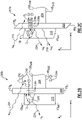
- FIG. 2A schematically illustrates a system 200a for characterizing structural defects in high-k dielectrics based on SHG, according to embodiments.
- the system 200a includes a semiconductor structure 202 comprising a semiconductor substrate 204 and a high-k dielectric layer 212 formed over the substrate 204, where the high-k dielectric layer 212 has electrically active structural defects, or traps 248 formed therein to be characterized.
- the semiconductor substrate 204 on which the high-k dielectric layer 212 can be implemented in a variety of ways, including, but not limited to, an n-doped or a p-doped semiconductor substrate, which can be formed of an elemental Group IV material (e.g., Si, Ge, C or Sn) or an alloy formed of Group IV materials (e.g., SiGe, SiGeC, SiC, SiSn, SiSnC, GeSn, etc.); Group III-V compound semiconductor materials (e.g., GaAs, GaN, InAs, etc.) or an alloy formed of Group III-V materials; Group II-VI semiconductor materials (CdSe, CdS, ZnSe, etc.) or an alloy formed of Group II-VI materials.
- an elemental Group IV material e.g., Si, Ge, C or Sn
- Group III-V compound semiconductor materials e.g., GaAs, GaN, InAs, etc.
- Group II-VI semiconductor materials CdS
- the substrate 204 can be implemented as a semiconductor on insulator, such as silicon on insulator (SOI) substrate.
- SOI substrate typically includes a silicon-insulator-silicon structure in which the various structures described above are isolated from a support substrate using an insulator layer such as a buried SiO 2 layer.
- insulator layer such as a buried SiO 2 layer.
- various structures described herein can be at least partially formed in an epitaxial layer formed at or near a surface region.
- the illustrated semiconductor structure 202 may be an intermediate device structures having certain regions formed therein, such that, subsequent to implementation of the method 100 ( FIG. 1 ) as part of an in-line characterization process, the semiconductor structure 202 can be further processed to form a functional MOS transistor.
- the semiconductor structure 202 may have doped regions such as heavily doped regions that when further processed, can serve as source and/or drain regions of a functional MOS transistor or other devices.
- the semiconductor structure 202 may further have isolation regions, e.g., shallow trench isolation regions.
- the illustrated semiconductor structure 202 may be a monitor structure having the high-k dielectric layer 212 formed thereon for the purposes of characterizing the structural defects formed therein for the purpose of, e.g., monitoring the health of a manufacturing tool or a line.
- the illustrated semiconductor structure 202 is illustrated as being a planar structure, embodiments are not so limited.
- the structure 202 may include a semiconductor substrate 204 having isolation regions formed therein and a fin-shaped semiconductor structure protruding vertically above the isolation regions, which can be further processed to form fin-shaped field effect transistors (FinFETs).
- FinFETs fin-shaped field effect transistors
- the high-k dielectric layer 212 may wrap around the fin-shaped semiconductor structure.
- a high-k dielectric refers to a dielectric material having a dielectric constant greater than that of SiO 2 .
- the high-k dielectric layer 212 may be a k-value greater than about 4, greater than about 8 or greater than about 15.
- the high-k dielectric layer 212 can be formed of Si 3 N 4 , Ta 2 O 5 , SrTiO 3 , ZrO 2 , HfO 2 , Al 2 O 3 , La 2 O 3 , Y 2 O 3 , HfSiO 4 and LaAlO 3 , including non-stoichiometric versions of the above and various mixtures thereof, as well combinations or stacks or nanolaminates thereof, to name a few.
- an interfacial layer 208 is formed between the substrate 204 and the high-k dielectric layer 212.
- the interfacial layer 212 can be formed of, e.g., SiOx or HfSiOx.
- the interfacial layer 208 can be formed unintentionally under some circumstances from oxygen precursors that diffuse to the high-k dielectric/substrate interface during the growth of the high-k dielectric layer 212 and/or bulk diffusion of excess oxygen atoms present in the high-k dielectric layer 212 during or after growth of the high-k dielectric layer 212.
- the interfacial layer 208 may be an intentionally grown SiO 2 layer to suppress the spontaneous growth of an interfacial oxide, and/or to provide better control of the properties of the interfacial layer and to provide a more stable surface for nucleation of the HfO 2 .
- the interfacial layer 208 may be omitted.
- the high-k dielectric layer 212 has structural defects, or traps 248 formed therein that are to be characterized using the methods and systems described herein.
- the defects 248 can be point defects, e.g., missing or extra atoms of the high-k layer 212.
- the traps 248 can include oxygen vacancies, which correspond to missing oxygen atoms, or interstitial oxygen atoms, which correspond to extra oxygen atoms.
- the traps 248 comprise vacancies, the traps 248 can be charged or neutral.
- oxygen vacancies in HfO 2 may exist in one of five charge states, namely +2, +1, 0, -1, and -2.
- the system 200a includes a light source 216, which can be a first light source comprising a laser, a lamp and/or light-emitting diode(s), among other light sources configured to direct incident light 220 having an incident energy hv 1 to the semiconductor structure 202 and at least partially propagate or transmit through the high-k dielectric layer 212 and further through the interfacial layer 208 when present.
- the light source 216 is further configured such that the incident light 220 is at least partially absorbed by the semiconductor substrate 204 to impart energy to the substrate 204 to cause elastic or inelastic processes therein.
- the light source 216 is configured to emit a monochromatic incident light 220 such that the partially transmitted incident light 220 having the incident energy is sufficient to cause charge carriers (e.g., electrons) to be at least transported from the semiconductor substrate to the traps 248 having a capture cross section ⁇ such that some of the charge carriers are temporarily trapped by the traps 248.
- charge carriers e.g., electrons
- the light source 216 operates in a wavelength range that is suitable for electron traps filled with temporarily trapped electrons to cause generation of light having an energy different from an incident energy resulting from nonlinear optical effects.
- the light source 216 may operate in a range between about 700 nm to about 2000 nm with a peak power between about 10 kW and 1 GW, according to embodiments.
- the light source 216 provides an intensity or a power density that is suitable for electron traps filled with temporarily trapped electrons to cause generation of light having an energy different from an incident energy resulting from nonlinear optical effects.
- the light source 216 may be configured to deliver an average power between about 10 mW and 10 about W or between about 100 mW and about 1 W, for instance about 300 mW.
- the incident light 220 having the incident energy is sufficient to cause SHG by the traps filled with charge carriers.
- harmonic generation can be observed in solids that do not possess a center symmetry.
- I ⁇ and I 2 ⁇ are the fundamental and second harmonic generation signal intensities, respectively, and ⁇ 2 and ⁇ 3 are the second-order and third-order susceptibilities, and E(t) is the electric field across the interface.
- SHG occurs, thereby generating SHG light 228 having double the frequency of the incident light 220.
- the system 200a further includes a detector 232 configured to measure a second harmonic spectrum resulting from the SHG light 228 having twice the energy of the incident light 220, and may also be configured to further measure or filter out reflected light 224 having the same energy as the incident light 220, according to embodiments.
- the detector 232 may be a photomultiplier tube, a CCD camera, an avalanche detector, a photodiode detector, a streak camera and a silicon detector, among other types of detectors.
- the light source 216 is shown as a sole light source, which can serves as a pump as well as a probe for generating as well as measuring the SHG light 228, embodiments are not so limited.
- a separate second light source (not shown), which can be a laser or a lamp, may be provided.
- the light source 216 may serve as one of a pump or a probe, while the second light source may serve as the other of the pump or the probe.
- the second light source when present, may operate in a wavelength range between about 80 nm and about 800 nm delivering an average power between about 10 mW and 10 W, according to embodiments.
- the system 200a may include various other optical elements.
- the system 200a may include: a photon counter; a reflective or refractive filter for selectively passing the SHG signal; a prism to differentiate the weaker SHG signal from the many-orders-of-magnitude-stronger reflected primary beam; a diffraction grating or a Pellicle beam splitter; an optical bundle for focusing and collimating/collimation optics; a filter wheel, zoom lens and/or polarizers.
- the system 200a further includes electronics or a time constant determining unit 246 configured to determine from the second harmonic spectrum one or both of a first time constant ( ⁇ 1 ) in the first region of the second harmonic spectrum that can be associated at least with a trapping rate of electrons by the traps 248, and a second time constant ( ⁇ 2 ) in the second region of the second harmonic spectrum that can be associated at least with a detrapping rate of electrons from the traps 248.
- a first time constant ( ⁇ 1 ) in the first region of the second harmonic spectrum that can be associated at least with a trapping rate of electrons by the traps 248, and a second time constant ( ⁇ 2 ) in the second region of the second harmonic spectrum that can be associated at least with a detrapping rate of electrons from the traps 248.
- the system 200a further includes electronics or a trap density determining unit 250 configured to determine a density of charge carrier traps in the high-k dielectric layer 212 based on the first time constant or both of the first time constant and the second time constant.
- the time constant determining unit 246 and the trap density determining unit 250 may be part of an electronic device 260, which may be a computing device, e.g., a field programmable gate array (e.g., FPGA), specially adapted for implementing the methods disclosed herein, as described more in detail infra.
- the electronic device 260 can be a computing device, a computer, a tablet, a microcontroller or a FPGA.
- the electronic device 260 includes a processor or processing electronics that may be configured to execute one or more software modules.
- the processor may be configured to execute one or more software applications, including a web browser, a telephone application, an email program, or any other software application.
- the electronic device 246 can implement the methods discussed herein by executing instructions included in a machine-readable non-transitory storage medium, such as a RAM, ROM, EEPROM, etc.
- the electronic device 246 can include a display device and/or a graphic user interface to interact with a user.
- the electronic device 246 can communicate with one or more devices over a network interface.
- the network interface can include transmitters, receivers and/or transceivers that can communicate over wired or wireless connections.
- FIG. 2B illustrates a schematic energy band diagram 200b of the semiconductor structure of the system 200a illustrated in FIG. 2A .
- the illustrated energy band diagram 200b corresponds to initial stages of measuring the SHG spectrum, e.g., the first region of the SHG spectrum.
- the high-k layer 212 has formed therein structural defects or traps 248 (represented as a distribution curve), which may be point defects as described above.
- the traps 248 may have a distribution of energy levels about a peak and/or a centroid having an energy level E T .
- the traps 248 may be distributed throughout the thickness of the high-k layer 212, while in other embodiments, the defects may be locally concentrated, e.g., near a high-k/semiconductor interface when the interlayer 208 is not present, or a high-k/interlayer interface when the interlayer 208 is present.
- the structural defects 248 are configured to trap electrons transported from the semiconductor substrate 204, according to some embodiments.
- the incident light having an energy hv 1 is partially absorbed in the semiconductor substrate 204 having a conduction band edge (CB SUB ) and a valence band edge (VB SUB ).
- CB SUB conduction band edge
- VB SUB valence band edge
- the semiconductor substrate 204 is undoped, relatively lightly doped (e.g., less than about 1 ⁇ 10 14 /cm 3 ) or p-doped, a relatively small concentration of electrons may be present in the conduction band.
- the energy hv 1 of the incident light 220 may be chosen such that hv 1 is greater than the band gap of the semiconductor substrate 204 by at least 0.1 eV or by at least 0.3 eV, such that electrons 240 (and/or holes 244) can be generated in the semiconductor substrate 204, to be transferred into the high-k dielectric layer to be trapped by the traps 248.
- the energy hv 1 of the incident light 220 is greater than the band gap of silicon at 1.12 eV (1110 nm) such that a sufficient amount of electrons 240 are populated in the conduction band.
- the incident light may be 1.2 eV or greater.
- the energy hv 1 of the incident light 220 need not be greater than the band gap of the semiconductor substrate 204. Instead, because the conduction band of the semiconductor 204 is already substantially populated with electrons 240, the energy hv 1 of the incident light 220 may impart additional energy to the electrons populated in the conduction band to be transferred into the high-k dielectric layer to be trapped by the traps 248.
- the electrons 240 may be transported through the thickness of the interlayer 208 when present, and/or at least partially through the thickness of the high-k dielectric layer 212, to be trapped by the structural defects or traps 248, as indicated by the arrows 238a.
- the electrons 240 may be transferred tunneling, e.g., directly tunneling or trap-assisted tunneling, from the conduction band of the substrate 204 into an energy level within the distribution of energy of traps 248.
- Direct tunneling of electrons is a quantum mechanical phenomenon, whose probability depends on the physical barrier thickness and height to be tunneled through by the electron, among other factors. Thus, the probability of tunneling is relatively higher when the potential barrier thickness and/or height are smaller.
- an initial state in the substrate 204) is at a higher potential than a final state (high-k dielectric layer 212).
- thermal relaxation may occur prior to tunneling, as indicated by the arrow 242.
- transfer mechanisms e.g., Poole-Frenkel conduction, Fowler-Norheim tunneling or thermionic emission, among other mechanisms.
- the physical thickness of the high-k dielectric 212 or the combined physical thicknesses of the high-k dielectric 212 and the interlayer 208 is about 5 nm or less, about 4 nm or less or about 3 nm or less, such that the electrons 220 can traverse a portion of the high-k dielectric layer 212 (and the interlayer 208 when present) to reach structural defects 248 within the bulk of the high-k dielectric layer 212.
- an effective oxide thickness (EOT) of the high-k dielectric layer 212 or the combination of high-k dielectric layer 212 and the interfacial layer 208 is between about 0.5 nm and about 3 nm, between about 0.5 nm and about 2.0 nm or between about 0.5 nm and 1.0 nm.
- the distribution of the defect energy of the traps 248 has a sufficient overlap with the conduction band edge (CB).
- CB conduction band edge
- a difference between the peak or the centroid energy E T of the defect energy distribution of traps 248 is about 2 eV or less, about 1 eV or less or about 0.5 eV or less.
- the E T is between a conduction band of the high-k dielectric layer 212 and a conduction band of the semiconductor substrate 204
- the exiting light 224 primarily comprise photons having the same energy hv 1 as the incident light 224.
- FIG. 2C illustrates a schematic energy band diagram 200c of the semiconductor structure of the system 200a illustrated in FIG. 2A .
- the illustrated energy band diagram 200c corresponds to later stages of measuring the SHG spectrum, e.g., the second region of the SHG spectrum.
- FIG. 2C illustrates a schematic energy band diagram 200c of the system 200a illustrated in FIG. 2A .
- the illustrated energy band diagram 200c corresponds to later stages compared to the energy band diagram 200b of FIG. 2B , during which the electrons trapped in the structural defects or traps 248 start to become detrapped.
- significant detrapping may begin, e.g., when a significant amount of electrons becomes trapped by the traps 248 such that an electric field builds up, thereby favoring back-tunneling of electrons 240 from the traps 248 to the conduction band of the silicon substrate 204, according to embodiments, as indicated by the arrows.
- the exiting light includes the SHG light 228 having twice the energy of the incident light 220, as well as the reflected light 224 having the same energy as the incident light 220.
- an SHG signal is weak compared to the reflected beam that produces it, it may be desirable to improve the signal-to-noise ratio of SHG counts.
- One method of reducing noise that may be employed is to actively cool the detector. The cooling can decrease the number of false-positive photon detections that are generated randomly because of thermal noise. This can be done using cryogenic fluids such as liquid nitrogen or helium or solid state cooling through use of a Peltier device.
- the method 100 includes, after measuring 112 a second harmonic spectrum, determining 116 from the second harmonic generation (SHG) spectrum a first time constant, which may be associated with a trapping rate of electrons by the traps 248 ( FIGS. 2A-2C ) and optionally in addition a second time constant, which may be associated with a detrapping rate of electrons from the traps 248.
- a first time constant which may be associated with a trapping rate of electrons by the traps 248 ( FIGS. 2A-2C ) and optionally in addition a second time constant, which may be associated with a detrapping rate of electrons from the traps 248.
- FIG. 3 illustrates a schematic SHG spectrum 400 for determining time constants and concentration of traps, according to embodiments.
- the spectrum 404 includes a relatively fast time-varying first region 404a at relatively short times of irradiation and a relatively slow time-varying second region 404b at relatively long times of irradiation.
- the first region 404a can correspond to the portion of the SHG spectrum 404 in which the SHG signal is dominated by increasing concentration of traps 248 having electrons trapped therein, as described above with respect to FIGS. 2A and 2B , thereby resulting in a relatively rapid increase (characterized by a first time constant ⁇ 1 ) in the SHG signal intensity.
- the effect of decreasing concentration of traps 248 by detrapping, as described above with respect to FIG. 2C is relatively small.
- the second region 404b can correspond to the portion of the SHG spectrum 404 in which the SHG signal is no longer dominated by increasing concentration of traps being filled by electrons as described above with respect to FIGS. 2A and 2B .
- the effect of decreasing concentration of structural defects having electrons trapped therein by detrapping, as described above with respect to FIGS. 2A and 2C is relatively large, thereby resulting in a relatively slow increase (characterized by a second time constant ⁇ 2 ) in the SHG spectrum.
- the first and second regions 404a and 404b of the SHG spectrum 404 can have the SHG signals that are proportional to the density of structural defects having electrons trapped therein, and can follow logarithmic time dependences.
- the logarithmic time dependences can be a function of the distance of filled traps 248 from the high-k dielectric/substrate interface or when the interlayer is present, the high-k dielectric/interlayer interface. That is, the trapping and detrapping rates increases with increasing tunneling distance, as described supra with respect to FIGS. 2B and 2C , due to decreasing transport probability with increasing tunneling distance.
- I 1 (t) and I 2 (t) correspond to SHG intensities in the first and second regions 404a and 404b of the SHG spectrum 404, respectively, and ⁇ 1 and ⁇ 2 are first and second time constants corresponding to the respective regions.
- the ⁇ 1 and ⁇ 2 can be obtained by, e.g., approximating the two regions 404a and 404b as approximately being independent SHG signals 408 and 412, respectively, as illustrated in FIG. 3 .
- ⁇ t is the capture cross section
- v th is the thermal velocity of electrons
- n c (x,t) is the density of electrons transported from, e.g., tunneled from, the silicon substrate into the high-k dielectric.
- the values of ⁇ t and v th can be obtained from independent theoretical or experimental determinations.
- nc(x,t) depends on tunneling probabilities, e.g., direct tunneling probabilities, of electrons from the substrate to the structural defects distributed within the high-k dielectric layer.
- nc(x,t) depends on several factors, including the energy and intensity of the incident light.
- the intensity and the energy of the incident light are sufficiently high such that substantially all of the traps in the high-k dielectric layer capture an electron, a substantially saturated SHG spectrum can be obtained.
- the energy of the incident light is sufficient for most of the electrons being transferred from the substrate to the traps have energies higher than most of the traps, and when the intensity of the incident light is sufficiently high such that the traps are rapidly filled, substantially all of the defects can have electrons captured therein before substantial detrapping occurs. Under such circumstance, a saturated SHG spectrum (not shown) can be obtained.
- a saturated SHG spectrum can have a relatively fast time-varying first portion at relatively short times of irradiation followed by a relatively time-independent constant second portion. That is, a saturated SHG spectrum can have a shape that is qualitatively similar to the deconvoluted SHG signal curve 408 of FIG. 3 .
- N t is the total concentration of traps, including filled and unfilled traps in the high-k dielectric layer.
- the N t can be obtained from ⁇ 1 alone, based on a quantitative correlation of completely filled N t to SHG intensity.
- the time constants can range between 0.1 femtosecond and 1 femtosecond, 1 femtosecond and 10 femtoseconds, 10 femtoseconds and 100 femtoseconds, 100 femtoseconds and 1 picosecond, between 1 picosecond and 10 picoseconds, between 10 picoseconds and 100 picoseconds, between 100 picoseconds and 1 nanosecond, between 1 nanosecond and 10 nanoseconds, between 10 nanosecond and 100 nanoseconds, between 100 nanoseconds and 1 microsecond, between 1 nanoseconds and 100 microseconds, between 100 microseconds and 1 millisecond, between 1 microsecond and 100 milliseconds, between 100 microsecond and 1 second, between 1 second and 10 seconds, or between 10 second and 100 seconds or larger or smaller.
- time delays ( ⁇ ) for example between the probe and pump (or pump and probe) can be, for example, between 0.1 femtosecond and 1 femtosecond, 1 femtosecond and 10 femtoseconds, 10 femtoseconds and 100 femtoseconds, 100 femtoseconds and 1 picosecond, between 1 picosecond and 10 picoseconds, between 10 picoseconds and 100 picoseconds, between 100 picoseconds and 1 nanosecond, between 1 nanosecond and 10 nanoseconds, between 10 nanosecond and 100 nanoseconds, between 100 nanoseconds and 1 microsecond, between 1 nanoseconds and 100 microseconds, between 100 microseconds and 1 millisecond, between 1 microsecond and 100 milliseconds, between 100 microsecond and 1 second, between 1 second and 10 seconds, between 10 second and 100 seconds. Values outside these ranges are also possible.
- the method 100 further includes, after determining ⁇ 1 and ⁇ 2 as described above, determining 120 a trap density in the high-k dielectric layer based on the one or both of the first time constant and the second time constant.
- nt(x,t) is the filled trap concentration profile in the high-k dielectric layer and N t is the total concentration of traps.
- one of the n t (x,t) and the N t can be determined by solving, e.g., numerically using a finite difference method, when the other of the nt(x,t) and the N t is used as inputs. For example, using nt(x,t) as an input, the differential Eq.
- [8] can be solved, e.g., numerically using a finite difference method, to obtain the total concentration of traps N t , according to embodiments.
- different profiles of nt(x,t) across the thickness of the high-k dielectric can be used as input, e.g., a constant profile, a normal profile and a delta function profile (e.g., at the high-k/SiO 2 interface), to name a few.
- the differential Eq. [8] can be solved, e.g., numerically using a finite difference method, to obtain nt(x,t), according to embodiments.
- the differential Eq. [8] can be solved to obtain time and spatial evolution of the filled trap concentration nt(x,t).
- SHG spectra are illustrated, as example implementations.
- the illustrated SHG spectra were measured from physical samples fabricated using atomic layer deposition.
- an HfO 2 film was grown by atomic layer deposition (ALD) on ⁇ 100> oriented Si substrate having a resistivity of about 1-5 Ohm-cm.
- ALD atomic layer deposition
- Each of the SHG spectra illustrated in FIGS. 5-7 were obtained using an incident light having photon energy of 1.5895 eV, which corresponds to the SHG photon energy of 3.179 eV, at an average laser power of 300 mW.
- the incident photon was directed to a surface of the HfO 2 film at about 45 degrees relative to the normal direction.
- FIG. 4 shows a graph 500 of an experimental second harmonic SHG spectrum 504 and a model fit 508 obtained using the method described supra, including numerically solving Eq. [8], according to embodiments.
- the experimental second harmonic SHG spectrum 504 was measured from Sample No. 7 in TABLE 1 above.
- each of the experimental SHG spectrum 504 and the model fit 508 shows a relatively fast time-varying first region at relatively short times (up to about 5 sec.) of irradiation, from which ⁇ 1 is obtained, followed by a relatively slow time-varying second region at relatively long times (beyond about 5 sec.) of irradiation, from which ⁇ 2 is obtained.
- the ⁇ 1 and ⁇ 2 values obtained were 2.6 sec. and 17 sec., respectively.
- the experimental SHG spectrum 504 and the model fit 508 are in excellent agreement.
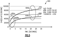
- FIG. 5 shows a graph 600 plotting experimental second harmonic SHG spectra 608 and 604 corresponding to Samples 7 and 9 having different H 2 O exposure times as described in TABLE 1 above.
- the experimental SHG spectra 608 and 604 show relatively fast time-varying first regions 608a and 604b, respectively, at relatively short times (up to about 5 sec.) of irradiation, followed by relatively slow time-varying second regions 608b and 604b, respectively, at relatively long times (beyond about 5 sec.) of irradiation.
- a comparison of the SHG spectra of the two samples suggests that longer duration of H 2 O pulses between Hf precursors results in higher efficiency of filling of the traps.
- FIG. 6 shows a graph 700 of experimental second harmonic SHG spectra 712, 608 and 704 corresponding to Samples 6, 7 and 9, respectively, having different nominal thicknesses as described in TABLE 1 above.
- the experimental SHG spectra 712, 608 and 704 show relatively fast time-varying first regions 712a, 608a and 704a, respectively, at relatively short times (up to about 5 sec.) of irradiation, followed by relatively slow time-varying second regions 712b, 608b and 704b, respectively, at relatively long times (beyond about 5 sec.) of irradiation.
- a comparison of the SHG spectra of the intensities and the time constants of the three samples shows that increasing thickness results an increasing ⁇ 1 and decreasing intensity in the fast time-varying first regions 712a, 608a and 704a.
- FIG. 7 shows a graph 800 correlating measured thicknesses for Samples 6-9 described in TABLE 1 and ⁇ 1 values obtained according to the methods described supra.
- Data points 816, 808, 812 and 804 correspond to Samples 6, 7, 8 and 9, respectively.
- the correlation suggests that increasing the thickness of the high-k layer may lead to an increased average time for electrons to transfer from the silicon substrate into the high-k dielectric layer, thus leading to higher ⁇ 1 values.
- the structural defects may not be concentrated at HfO 2 /SiO 2 or HfO 2 /Si interfaces, but instead distributed throughout the thicknesses of the HfO 2 films, thereby leading to lower probability of electron injection from the silicon substrate into structural defects in the HfO 2 films.
- DSP Digital Signal Processor
- ASIC Application Specific Integrated Circuit
- FPGA Field Programmable Gate Array
- a general purpose processor may be a microprocessor, but in the alternative, the processor may be any conventional processor, controller, microcontroller, or state machine.
- the processor can be part of a computer system that also has a user interface port that communicates with a user interface, and which receives commands entered by a user, has at least one memory (e.g., hard drive or other comparable storage, and random access memory) that stores electronic information including a program that operates under control of the processor and with communication via the user interface port, and a video output that produces its output via any kind of video output format, e.g., VGA, DVI, HDMI, DisplayPort, or any other form.
- a user interface port that communicates with a user interface, and which receives commands entered by a user
- has at least one memory e.g., hard drive or other comparable storage, and random access memory
- stores electronic information including a program that operates under control of the processor and with communication via the user interface port, and a video output that produces its output via any kind of video output format, e.g., VGA, DVI, HDMI, DisplayPort, or any other form.
- a processor may also be implemented as a combination of computing devices, e.g., a combination of a DSP and a microprocessor, a plurality of microprocessors, one or more microprocessors in conjunction with a DSP core, or any other such configuration. These devices may also be used to select values for devices as described herein.
- a software module may reside in Random Access Memory (RAM), flash memory, Read Only Memory (ROM), Electrically Programmable ROM (EPROM), Electrically Erasable Programmable ROM (EEPROM), registers, hard disk, a removable disk, a CD-ROM, or any other form of storage medium known in the art.
- An exemplary storage medium is coupled to the processor such that the processor can read information from, and write information to, the storage medium.
- the storage medium may be integral to the processor.
- the processor and the storage medium may reside in an ASIC.
- the ASIC may reside in a user terminal.
- the processor and the storage medium may reside as discrete components in a user terminal.
- the functions described may be implemented in hardware, software, firmware, or any combination thereof. If implemented in software, the functions may be stored on, transmitted over or resulting analysis/calculation data output as one or more instructions, code or other information on a computer-readable medium.
- Computer-readable media includes both computer storage media and communication media including any medium that facilitates transfer of a computer program from one place to another.
- a storage media may be any available media that can be accessed by a computer.
- such computer-readable media can comprise RAM, ROM, EEPROM, CD-ROM or other optical disk storage, magnetic disk storage or other magnetic storage devices, or any other medium that can be used to carry or store desired program code in the form of instructions or data structures and that can be accessed by a computer.
- the memory storage can also be rotating magnetic hard disk drives, optical disk drives, or flash memory based storage drives or other such solid state, magnetic, or optical storage devices.
- any connection is properly termed a computer-readable medium.
- the software is transmitted from a website, server, or other remote source using a coaxial cable, fiber optic cable, twisted pair, digital subscriber line (DSL), or wireless technologies such as infrared, radio, and microwave
- the coaxial cable, fiber optic cable, twisted pair, DSL, or wireless technologies such as infrared, radio, and microwave are included in the definition of medium.
- Disk and disc includes compact disc (CD), laser disc, optical disc, digital versatile disc (DVD), floppy disk and Blu-ray disc where disks usually reproduce data magnetically, while discs reproduce data optically with lasers. Combinations of the above should also be included within the scope of computer-readable media.
- Operations as described herein can be carried out on or over a website.
- the website can be operated on a server computer, or operated locally, e.g., by being downloaded to the client computer, or operated via a server farm.
- the website can be accessed over a mobile phone or a PDA, or on any other client.
- the website can use HTML code in any form, e.g., MHTML, or XML, and via any form such as cascading style sheets (“CSS”) or other.
- the computers described herein may be any kind of computer, either general purpose, or some specific purpose computer such as a workstation.
- the programs may be written in C, or Java, Brew or any other programming language.
- the programs may be resident on a storage medium, e.g., magnetic or optical, e.g. the computer hard drive, a removable disk or media such as a memory stick or SD media, or other removable medium.
- the programs may also be run over a network, for example, with a server or other machine sending signals to the local machine, which allows the local machine to carry out the operations described herein.
Landscapes
- Physics & Mathematics (AREA)
- General Physics & Mathematics (AREA)
- Health & Medical Sciences (AREA)
- Chemical & Material Sciences (AREA)
- Life Sciences & Earth Sciences (AREA)
- Analytical Chemistry (AREA)
- Biochemistry (AREA)
- General Health & Medical Sciences (AREA)
- Immunology (AREA)
- Pathology (AREA)
- Engineering & Computer Science (AREA)
- Nuclear Medicine, Radiotherapy & Molecular Imaging (AREA)
- Spectroscopy & Molecular Physics (AREA)
- Nonlinear Science (AREA)
- Optics & Photonics (AREA)
- Computer Vision & Pattern Recognition (AREA)
- Signal Processing (AREA)
- General Engineering & Computer Science (AREA)
- Chemical Kinetics & Catalysis (AREA)
- Mathematical Physics (AREA)
- Theoretical Computer Science (AREA)
- Testing Or Measuring Of Semiconductors Or The Like (AREA)
- Manufacturing & Machinery (AREA)
- Computer Hardware Design (AREA)
- Microelectronics & Electronic Packaging (AREA)
- Power Engineering (AREA)
Claims (15)
- Verfahren (100) zum Charakterisieren einer Halbleiterstruktur, das Verfahren umfassend:Bereitstellen (104) einer Halbleiterstruktur (202), umfassend einen Halbleiter und eine über dem Halbleiter gebildete dielektrische Schicht (212) mit hohem k-Wert, wobei in der dielektrischen Schicht mit hohem k-Wert Elektronenfallen (248) gebildet sind;zumindest teilweises Übertragen (108) eines einfallenden Lichts, das eine einfallende Energie aufweist, durch die dielektrische Schicht mit hohem k-Wert und zumindest teilweises Absorbieren des einfallenden Lichts in dem Halbleiter,wobei die einfallende Energie ausreichend ist, um zu bewirken, dass Elektronen von dem Halbleiter zu den Elektronenfallen (248) transportiert werden, sodass einige der Elektronen vorübergehend von den Elektronenfallen eingefangen werden, undwobei die einfallende Energie ausreichend ist, damit die mit vorübergehend gefangenen Elektronen gefüllten Elektronenfallen (248) eine Erzeugung von Licht bewirken, das eine Energie aufweist, die sich von der einfallenden Energie unterscheidet, die aus nichtlinearen optischen Effekten resultiert;Erlangen eines nichtlinearen Spektrums, das aus dem Licht resultiert, das eine Energie aufweist, die sich von der einfallenden Energie unterscheidet, wobei das Spektrum eine Messung der Intensität über die Zeit ist, wobei das nichtlineare Spektrum einen ersten Bereich (404a, 604a, 608a, 704a, 712a) und einen zweiten Bereich (404b, 604b, 608b, 704b, 712b), der auf den ersten Bereich folgt, aufweist, wobei eine Intensität in dem ersten Bereich mit einer schnelleren Rate im Vergleich zu dem zweiten Bereich zunimmt;Bestimmen (116) einer ersten Zeitkonstante aus dem ersten Bereich und optional einer zweiten Zeitkonstante aus dem zweiten Bereich aus dem Spektrum; dadurch gekennzeichnet, dass das Verfahren ferner Folgendes umfasstBestimmen (120) einer Elektronenfallendichte in der dielektrischen Schicht basierend auf der ersten Zeitkonstante oder sowohl der ersten Zeitkonstante als auch der zweiten Zeitkonstante.
- Verfahren nach Anspruch 1, wobei ein Bereitstellen der Halbleiterstruktur (202) ein Bereitstellen einer dielektrischen Schicht mit hohem k-Wert auf Hf-Basis auf einem Siliziumsubstrat umfasst.
- Verfahren nach Anspruch 2, wobei ein Bereitstellen der Halbleiterstruktur (202) ferner ein Bereitstellen einer Siliziumdioxidschicht umfasst, die zwischen dem Siliziumsubstrat und der dielektrischen Schicht mit hohem k-Wert auf Hf-Basis eingefügt ist.
- Verfahren nach Anspruch 3, wobei die kombinierte physische Stärke der Siliziumdioxidschicht und der dielektrischen Schicht mit hohem k-Wert auf Hf-Basis weniger als 4 nm ist, sodass die Elektronen durch Tunneln vom Siliziumsubstrat zu den Elektronenfallen innerhalb einer Zeitdauer der Messung des nichtlinearen optischen Spektrums von dem Siliziumsubstrat zu den Sauerstofflücken transportiert werden können.
- Verfahren nach Anspruch 1, wobei die Elektronenfallen (248) Sauerstofflücken umfassen, oder wobei die Elektronenfallen ein mittleres Fallenenergieniveau aufweisen, das zwischen einem Leitungsband der dielektrischen Schicht mit hohem k-Wert (212) und einem Leitungsband des Halbleitersubstrats ist.
- Verfahren nach Anspruch 1, wobei die erste Zeitkonstante in dem ersten Bereich zumindest mit einer Einfangrate von Elektronen durch die Elektronenfallen (248) assoziiert ist, und wobei die zweite Zeitkonstante in dem zweiten Bereich zumindest mit einer Freilassrate von Elektronen aus den Elektronenfallen assoziiert ist.
- Verfahren nach Anspruch 1, umfassend ein Bestimmen sowohl der ersten Zeitkonstante aus dem ersten Bereich als auch der zweiten Zeitkonstante aus dem zweiten Bereich aus dem nichtlinearen optischen Spektrum und Bestimmen der Fallendichte in der dielektrischen Schicht mit hohem k-Wert (212) basierend sowohl auf der ersten Zeitkonstante als auch der zweiten Zeitkonstante.
- Verfahren nach Anspruch 7, wobei ein Bestimmen der Fallendichte ein numerisches Lösen einer partiellen Differentialgleichung umfasst, die eine Änderungsrate der gefüllten Fallen mit den Inversen der ersten Zeitkonstante und der zweiten Zeitkonstante in Beziehung setzt.
- Verfahren nach Anspruch 8, wobei die partielle Differentialgleichung wie folgt ausgedrückt wird:

- Verfahren nach einem der Ansprüche 1-9, wobei die einfallende Energie ausreichend ist, damit die mit vorübergehend eingefangenen Elektronen gefüllten Elektronenfallen eine SHG-Erzeugung zweiter Oberschwingung bewirken, und wobei ein Messen des nichtlinearen optischen Spektrums ein Messen eines Spektrums der zweiten Oberschwingung umfasst, die den dem ersten Bereich und den zweiten Bereich aufweist.
- System (200a) zum Charakterisieren einer Halbleiterstruktur (202), das System umfassend:eine Lichtquelle (216), die konfiguriert ist, um ein einfallendes Licht (220) zu emittieren, das Einfallsenergie aufweist, die zumindest teilweise durch eine auf einem Halbleiter ausgebildete dielektrische Schicht mit hohem k-Wert (212) übertragen und zumindest teilweise von dem Halbleiter absorbiert wird, wobei die dielektrische Schicht mit hohem k-Wert (212) darin gebildete Elektronenfallen (248) aufweist,wobei die einfallende Energie ausreichend ist, um zu bewirken, dass Elektronen von dem Halbleiter zu den Elektronenfallen (248) transportiert werden, sodass einige der Elektronen vorübergehend von den Elektronenfallen eingefangen werden, undwobei die einfallende Energie ausreichend ist, damit die mit vorübergehend gefangenen Elektronen gefüllten Elektronenfallen (248) eine Erzeugung von Licht bewirken, das eine Energie aufweist, die sich von der einfallenden Energie unterscheidet, die aus nichtlinearen optischen Effekten resultiert;einen Detektor (232), der konfiguriert ist, um ein nichtlineares Spektrum zu messen, das aus dem Licht resultiert, das eine Energie aufweist, die sich von der einfallenden Energie unterscheidet, wobei das Spektrum eine Messung der Intensität über die Zeit ist, wobei das nichtlineare Spektrum einen ersten Bereich (404a, 604a, 608a, 704a, 712a) und einen zweiten Bereich (404b, 604b, 608b, 704b, 712b), der auf den ersten Bereich folgt, aufweist, wobei die Intensität in dem ersten Bereich mit einer schnelleren Rate im Vergleich zu dem zweiten Bereich zunimmt; undElektronik (260), umfassend eine Zeitkonstanten-Bestimmungseinheit (246), die konfiguriert ist, um aus dem Spektrum eine erste Zeitkonstante aus dem ersten Bereich und optional eine zweite Zeitkonstante aus dem zweiten Bereich zu bestimmen (116), dadurch gekennzeichnet, dass die Elektronik (260) ferner eine Fallendichte-Bestimmungseinheit (250) umfasst, die konfiguriert ist, um eine Elektronenfallendichte in der dielektrischen Schicht basierend auf der ersten Zeitkonstante oder sowohl der ersten Zeitkonstante als auch der zweiten Zeitkonstante zu bestimmen(120).
- System nach Anspruch 11, wobei die dielektrische Schicht mit hohem k-Wert eine Schicht mit hohem k-Wert auf Hf-Basis ist und der Halbleiter aus Silizium gebildet ist, oder wobei die Elektronenfallen (248) Sauerstofflücken umfassen, oder wobei die Elektronenfallen ein mittleres Fallenenergieniveau aufweisen, das zwischen einem Leitungsband der Schicht mit hohem k-Wert und einem Leitungsband des Halbleiters ist.
- System nach Anspruch 11, wobei die Lichtquelle konfiguriert ist, um das einfallende Licht zumindest teilweise durch eine Siliziumdioxidschicht weiter zu übertragen, die zwischen der dielektrischen Schicht mit hohem k-Wert (212) und dem Halbleiter eingefügt ist.
- System nach Anspruch 13, wobei die kombinierte physische Stärke der Siliziumdioxidschicht und der Schicht mit hohem k-Wert auf Hf-Basis weniger als 4 nm ist, sodass die Elektronen durch direktes Tunneln von dem Halbleiter zu den Elektronenfallen (248) innerhalb einer Zeitspanne der Messung des nichtlinearen optischen Spektrums von dem Halbleiter zu den Sauerstofflücken transportiert werden können.
- System nach einem der Ansprüche 11-14, wobei die einfallende Energie ausreichend ist, damit die mit vorübergehend eingefangenen Elektronen gefüllten Elektronenfallen eine SHG-Erzeugung zweiter Oberschwingung bewirken, und wobei ein Messen des nichtlinearen optischen Spektrums ein Messen eines Spektrums der zweiten Oberschwingung umfasst, die den dem ersten Bereich und den zweiten Bereich aufweist.
Applications Claiming Priority (3)
| Application Number | Priority Date | Filing Date | Title |
|---|---|---|---|
| US201562213753P | 2015-09-03 | 2015-09-03 | |
| US201562237146P | 2015-10-05 | 2015-10-05 | |
| PCT/US2016/050286 WO2017041049A1 (en) | 2015-09-03 | 2016-09-02 | Optical systems and methods of characterizing high-k dielectrics |
Publications (3)
| Publication Number | Publication Date |
|---|---|
| EP3344972A1 EP3344972A1 (de) | 2018-07-11 |
| EP3344972A4 EP3344972A4 (de) | 2019-03-27 |
| EP3344972B1 true EP3344972B1 (de) | 2022-12-14 |
Family
ID=58188669
Family Applications (1)
| Application Number | Title | Priority Date | Filing Date |
|---|---|---|---|
| EP16843152.6A Active EP3344972B1 (de) | 2015-09-03 | 2016-09-02 | Optische systeme und verfahren zur charakterisierung von high-k-dielektrika |
Country Status (5)
| Country | Link |
|---|---|
| US (2) | US10989664B2 (de) |
| EP (1) | EP3344972B1 (de) |
| KR (1) | KR102533125B1 (de) |
| CN (2) | CN108369186B (de) |
| WO (1) | WO2017041049A1 (de) |
Families Citing this family (15)
| Publication number | Priority date | Publication date | Assignee | Title |
|---|---|---|---|---|
| WO2015161136A1 (en) | 2014-04-17 | 2015-10-22 | Femtometrix, Inc. | Wafer metrology technologies |
| US10551325B2 (en) | 2014-11-12 | 2020-02-04 | Femtometrix, Inc. | Systems for parsing material properties from within SHG signals |
| CN108369186B (zh) | 2015-09-03 | 2022-05-27 | 加州理工学院 | 表征高k介质的光学系统以及方法 |
| US10163493B2 (en) * | 2017-05-08 | 2018-12-25 | International Business Machines Corporation | SRAM margin recovery during burn-in |
| KR20210021292A (ko) | 2018-04-27 | 2021-02-25 | 펨토매트릭스, 인코포레이티드. | 반도체 장치들의 특성들을 판단하는 시스템들 및 방법들 |
| WO2019222260A1 (en) | 2018-05-15 | 2019-11-21 | Femtometrix, Inc. | Second harmonic generation (shg) optical inspection system designs |
| US10901054B1 (en) * | 2018-05-25 | 2021-01-26 | Hrl Laboratories, Llc | Integrated optical waveguide and electronic addressing of quantum defect centers |
| JP2020035980A (ja) * | 2018-08-31 | 2020-03-05 | 株式会社サイオクス | エピタキシャル基板 |
| CN111326433B (zh) * | 2018-12-17 | 2024-01-19 | 紫创(南京)科技有限公司 | 半导体检测装置及检测方法 |
| EP3913356B1 (de) * | 2020-05-18 | 2025-01-22 | Imec VZW | Verfahren zur messung der fallendichte in einem 2-dimensionalen halbleitermaterial |
| CN111855704B (zh) * | 2020-07-28 | 2024-01-12 | 哈尔滨工业大学 | 双极晶体管电离损伤敏感部位的检测方法 |
| US12094787B2 (en) * | 2021-08-03 | 2024-09-17 | Applied Materials, Inc. | Characterizing defects in semiconductor layers |
| KR102708172B1 (ko) * | 2022-04-06 | 2024-09-20 | 동국대학교 산학협력단 | 반도체 소자의 분석 방법 및 이를 위한 분석 장치 |
| CN119768662A (zh) * | 2022-06-15 | 2025-04-04 | 菲拓梅里克斯公司 | 使用非线性光学器件的尺寸计量 |
| US20240176206A1 (en) * | 2022-11-29 | 2024-05-30 | Kla Corporation | Interface-based thin film metrology using second harmonic generation |
Family Cites Families (86)
| Publication number | Priority date | Publication date | Assignee | Title |
|---|---|---|---|---|
| CH538687A (de) | 1971-11-23 | 1973-06-30 | Bbc Brown Boveri & Cie | Verfahren und Einrichtung zur Untersuchung der Störstellenkonzentration von Halbleitern |
| JPS55138438A (en) | 1979-04-16 | 1980-10-29 | Olympus Optical Co | Automatic exposing device for endoscope |
| US4286215A (en) | 1979-05-18 | 1981-08-25 | Bell Telephone Laboratories, Incorporated | Method and apparatus for the contactless monitoring carrier lifetime in semiconductor materials |
| US4812756A (en) | 1987-08-26 | 1989-03-14 | International Business Machines Corporation | Contactless technique for semicondutor wafer testing |
| DE68925810T2 (de) | 1989-01-13 | 1996-09-26 | Ibm | Verfahren und Vorrichtung zur Erzeugung von blaugrüner Lichtstrahlung |
| JPH0816607B2 (ja) | 1990-10-30 | 1996-02-21 | インターナショナル・ビジネス・マシーンズ・コーポレイション | 薄膜処理制御方法 |
| US5557409A (en) | 1994-10-13 | 1996-09-17 | Advanced Micro Devices Inc. | Characterization of an external silicon interface using optical second harmonic generation |
| FR2726369B1 (fr) | 1994-11-02 | 1996-12-20 | Alcatel Cable | Procede de mesure du declin de potentiel et de la mobilite electronique d'un materiau |
| US6321601B1 (en) | 1996-08-06 | 2001-11-27 | Brown University Research Foundation | Optical method for the characterization of laterally-patterned samples in integrated circuits |
| US5814820A (en) | 1996-02-09 | 1998-09-29 | The Board Of Trustees Of The University Of Illinois | Pump probe cross correlation fluorescence frequency domain microscope and microscopy |
| US6483580B1 (en) | 1998-03-06 | 2002-11-19 | Kla-Tencor Technologies Corporation | Spectroscopic scatterometer system |
| US6856159B1 (en) | 1999-03-18 | 2005-02-15 | Vanderbilt University | Contactless optical probe for use in semiconductor processing metrology |
| WO2000055885A1 (en) | 1999-03-18 | 2000-09-21 | Vanderbilt University | Contactless optical probe for use in semiconductor processing metrology |
| US7158284B2 (en) | 1999-03-18 | 2007-01-02 | Vanderbilt University | Apparatus and methods of using second harmonic generation as a non-invasive optical probe for interface properties in layered structures |
| US6512385B1 (en) | 1999-07-26 | 2003-01-28 | Paul Pfaff | Method for testing a device under test including the interference of two beams |
| US6147799A (en) | 1999-10-08 | 2000-11-14 | Agilent Technologies Inc. | Physically compact variable optical delay element having wide adjustment range |
| US6356377B1 (en) | 1999-11-10 | 2002-03-12 | Agere Systems Guardian Corp. | Mems variable optical delay lines |
| US6587258B1 (en) * | 2000-03-24 | 2003-07-01 | Southwest Sciences Incorporated | Electro-optic electric field probe |
| JP2002091512A (ja) | 2000-09-12 | 2002-03-29 | Meidensha Corp | シーケンサのプログラミング支援装置 |
| US6900894B2 (en) * | 2000-11-16 | 2005-05-31 | Process Diagnostics, Inc. | Apparatus and method for measuring dose and energy of ion implantation by employing reflective optics |
| US6791099B2 (en) | 2001-02-14 | 2004-09-14 | Applied Materials, Inc. | Laser scanning wafer inspection using nonlinear optical phenomena |
| US6650800B2 (en) | 2001-03-19 | 2003-11-18 | General Instrument Corporation | Time slot tunable all-optical packet data demultiplexer |
| JP2004535595A (ja) | 2001-04-12 | 2004-11-25 | オムニガイド コミュニケーションズ インコーポレイテッド | 高屈折率コントラストの光導波路および用途 |
| US20030148391A1 (en) | 2002-01-24 | 2003-08-07 | Salafsky Joshua S. | Method using a nonlinear optical technique for detection of interactions involving a conformational change |
| US6795175B2 (en) | 2002-05-21 | 2004-09-21 | The Boeing Company | System and method for imaging contamination on a surface |
| US6788405B2 (en) | 2002-06-12 | 2004-09-07 | The Boeing Company | Nonlinear optical system for sensing the presence of contamination on a semiconductor wafer |
| US7304305B2 (en) | 2002-06-19 | 2007-12-04 | The Boeing Company | Difference-frequency surface spectroscopy |
| US6882414B2 (en) | 2002-06-19 | 2005-04-19 | The Boeing Company | Broadband infrared spectral surface spectroscopy |
| US6781686B2 (en) | 2002-06-19 | 2004-08-24 | The Boeing Company | Femtosecond optical surface imaging |
| US6819844B2 (en) | 2002-06-20 | 2004-11-16 | The Boeing Company | Fiber-optic based surface spectroscopy |
| AU2002321147A1 (en) | 2002-06-28 | 2004-01-19 | Pirelli & C. S.P.A. | Four-wave-mixing based optical wavelength converter device |
| US7248062B1 (en) | 2002-11-04 | 2007-07-24 | Kla-Tencor Technologies Corp. | Contactless charge measurement of product wafers and control of corona generation and deposition |
| JP3918054B2 (ja) | 2003-01-23 | 2007-05-23 | 独立行政法人物質・材料研究機構 | 物質の光応答を測定する方法およびその装置 |
| KR101159070B1 (ko) * | 2003-03-11 | 2012-06-25 | 삼성전자주식회사 | 고유전율 산화막 형성방법, 이 방법으로 형성된 유전막이구비된 커패시터 및 그 제조방법 |
| JP2004311580A (ja) | 2003-04-03 | 2004-11-04 | Toshiba Corp | 半導体評価装置及び半導体評価方法 |
| JP2005035235A (ja) | 2003-07-18 | 2005-02-10 | Noritsu Koki Co Ltd | 画像露光装置 |
| US20050058165A1 (en) | 2003-09-12 | 2005-03-17 | Lightwave Electronics Corporation | Laser having <100>-oriented crystal gain medium |
| GB2424069B (en) | 2003-11-25 | 2007-11-14 | Univ Leland Stanford Junior | Method for determining the optical nonlinearity profile of a material |
| US7362496B2 (en) | 2004-04-20 | 2008-04-22 | The Boeing Company | Fiber gain medium and method of coupling pump energy into the same |
| KR100688521B1 (ko) * | 2005-01-18 | 2007-03-02 | 삼성전자주식회사 | 고유전율 절연막을 포함하는 반도체 소자 및 그 제조 방법 |
| US7202691B2 (en) | 2005-05-31 | 2007-04-10 | Semiconductor Diagnostics, Inc. | Non-contact method for acquiring charge-voltage data on miniature test areas of semiconductor product wafers |
| US7602009B2 (en) * | 2005-06-16 | 2009-10-13 | Micron Technology, Inc. | Erasable non-volatile memory device using hole trapping in high-K dielectrics |
| US7580138B2 (en) | 2005-07-12 | 2009-08-25 | Sematech, Inc. | Methods and systems for characterizing semiconductor materials |
| US7433056B1 (en) | 2005-07-15 | 2008-10-07 | Kla-Tencor Technologies Corporation | Scatterometry metrology using inelastic scattering |
| US7893703B2 (en) | 2005-08-19 | 2011-02-22 | Kla-Tencor Technologies Corp. | Systems and methods for controlling deposition of a charge on a wafer for measurement of one or more electrical properties of the wafer |
| WO2007049259A1 (en) | 2005-10-24 | 2007-05-03 | Optical Metrology Patents Limited | An optical measurement apparatus and method |
| US7718969B2 (en) | 2005-12-27 | 2010-05-18 | Rensselaer Polytechnic Institute | Methods and systems for generating amplified terahertz radiation for analyzing remotely-located objects |
| KR100683384B1 (ko) * | 2005-12-30 | 2007-02-15 | 동부일렉트로닉스 주식회사 | 반도체 소자의 계면 전하포획 밀도 측정 방법 |
| JP4996856B2 (ja) | 2006-01-23 | 2012-08-08 | 株式会社日立ハイテクノロジーズ | 欠陥検査装置およびその方法 |
| US7595204B2 (en) * | 2006-03-07 | 2009-09-29 | Sematech, Inc. | Methods and systems for determining trapped charge density in films |
| US7894126B2 (en) | 2006-04-21 | 2011-02-22 | Eth Zurich | Broadband Terahertz radiation generation and detection system and method |
| US7537804B2 (en) * | 2006-04-28 | 2009-05-26 | Micron Technology, Inc. | ALD methods in which two or more different precursors are utilized with one or more reactants to form materials over substrates |
| US7659979B2 (en) | 2006-10-17 | 2010-02-09 | Kla-Tencor Corporation | Optical inspection apparatus and method |
| US7684047B2 (en) | 2006-10-27 | 2010-03-23 | Lockheed Martin Corporation | Apparatus and method for two wave mixing (TWM) based ultrasonic laser testing |
| KR101146589B1 (ko) * | 2006-11-30 | 2012-05-16 | 삼성전자주식회사 | 전하 트랩형 반도체 메모리 소자 |
| JP5109123B2 (ja) | 2007-03-08 | 2012-12-26 | 国立大学法人東京工業大学 | 電界分布又はキャリア分布を高次高調波の強度に基づいて検出する検出装置及びその検出方法 |
| US7830527B2 (en) | 2007-04-13 | 2010-11-09 | The United States Of America As Represented By The Administrator Of The National Aeronautics And Space Administration | Multiple frequency optical mixer and demultiplexer and apparatus for remote sensing |
| US8525287B2 (en) * | 2007-04-18 | 2013-09-03 | Invisage Technologies, Inc. | Materials, systems and methods for optoelectronic devices |
| US7982944B2 (en) | 2007-05-04 | 2011-07-19 | Max-Planck-Gesellschaft Zur Forderung Der Wissenschaften E.V. | Method and apparatus for optical frequency comb generation using a monolithic micro-resonator |
| US9285338B2 (en) * | 2007-07-19 | 2016-03-15 | University of Pittsburgh—of the Commonwealth System of Higher Education | Separation of particles using multiplexed dielectrophoresis |
| US20100208757A1 (en) | 2007-07-31 | 2010-08-19 | Ye Hu | Method of ferroelectronic domain inversion and its applications |
| US7781739B1 (en) * | 2008-03-12 | 2010-08-24 | Physical Optics Corporation | Quantum-imaging system and mode of operation and method of fabrication thereof |
| EP2211343A1 (de) | 2009-01-27 | 2010-07-28 | Thomson Licensing | Optisches Aufzeichnungsmedium für hohe Datendichte |
| JP2010190722A (ja) | 2009-02-18 | 2010-09-02 | Hitachi High-Technologies Corp | 欠陥検査方法及び欠陥検査装置 |
| US20100272134A1 (en) | 2009-04-22 | 2010-10-28 | Blanding Douglass L | Rapid Alignment Methods For Optical Packages |
| BR112012024411A2 (pt) | 2010-03-31 | 2016-05-31 | Kaneka Corp | estrutura, chip para sensor de ressonância de plásmon de superfície localizada, sensor de ressonância de plásmon de superfície localizada e métodos de fabricação |
| US8573785B2 (en) | 2010-11-23 | 2013-11-05 | Corning Incorporated | Wavelength-switched optical systems |
| CN102353882B (zh) * | 2011-06-09 | 2014-02-19 | 北京大学 | 一种半导体器件的栅介质层陷阱密度和位置的测试方法 |
| US8755044B2 (en) | 2011-08-15 | 2014-06-17 | Kla-Tencor Corporation | Large particle detection for multi-spot surface scanning inspection systems |
| US9652729B2 (en) | 2011-10-27 | 2017-05-16 | International Business Machines Corporation | Metrology management |
| CN102522386B (zh) * | 2011-12-02 | 2014-06-11 | 北京大学 | 栅氧化层界面陷阱密度测试结构及测试方法 |
| US20150287842A1 (en) * | 2011-12-16 | 2015-10-08 | Dow Global Technologies Llc | Photovoltaic system including light trapping filtered optical module |
| US9194908B2 (en) | 2012-03-28 | 2015-11-24 | Infinitum Solutions, Inc. | Metrology for contactless measurement of electrical resistance change in magnetoresistive samples |
| WO2015187221A2 (en) * | 2014-03-06 | 2015-12-10 | California Institute Of Technology | Systems and methods for implementing electrically tunable metasurfaces |
| WO2015161136A1 (en) | 2014-04-17 | 2015-10-22 | Femtometrix, Inc. | Wafer metrology technologies |
| WO2016007950A1 (en) | 2014-07-11 | 2016-01-14 | Vanderbilt Universtiy | Apparatus and methods for probing a material as a function of depth using depth-dependent second harmonic generation |
| US10551325B2 (en) | 2014-11-12 | 2020-02-04 | Femtometrix, Inc. | Systems for parsing material properties from within SHG signals |
| US9851589B2 (en) * | 2015-08-10 | 2017-12-26 | Samsung Electronics Co., Ltd. | Meta-structure and tunable optical device including the same |
| CN108369186B (zh) | 2015-09-03 | 2022-05-27 | 加州理工学院 | 表征高k介质的光学系统以及方法 |
| JP6604629B2 (ja) | 2016-02-15 | 2019-11-13 | 株式会社Screenホールディングス | 検査装置及び検査方法 |
| US10274807B2 (en) * | 2016-12-08 | 2019-04-30 | Northwestern University | Optical quantification of interfacial charge states |
| US10274310B2 (en) | 2016-12-22 | 2019-04-30 | The Boeing Company | Surface sensing systems and methods for imaging a scanned surface of a sample via sum-frequency vibrational spectroscopy |
| KR20210021292A (ko) | 2018-04-27 | 2021-02-25 | 펨토매트릭스, 인코포레이티드. | 반도체 장치들의 특성들을 판단하는 시스템들 및 방법들 |
| EP3785022A4 (de) | 2018-04-27 | 2022-02-23 | SK Hynix Inc. | Feldverzerrte nichtlineare optische metrologie mit einer koronaentladungsquelle |
| WO2019222260A1 (en) | 2018-05-15 | 2019-11-21 | Femtometrix, Inc. | Second harmonic generation (shg) optical inspection system designs |
| US10976358B2 (en) * | 2018-11-07 | 2021-04-13 | The Boeing Company | Surface charging systems and method for charging a non-planar surface |
-
2016
- 2016-09-02 CN CN201680064010.9A patent/CN108369186B/zh active Active
- 2016-09-02 EP EP16843152.6A patent/EP3344972B1/de active Active
- 2016-09-02 KR KR1020187009474A patent/KR102533125B1/ko active Active
- 2016-09-02 WO PCT/US2016/050286 patent/WO2017041049A1/en not_active Ceased
- 2016-09-02 US US15/256,442 patent/US10989664B2/en active Active
- 2016-09-02 CN CN202210501568.6A patent/CN115096826A/zh active Pending
-
2021
- 2021-01-12 US US17/147,371 patent/US11808706B2/en active Active
Also Published As
| Publication number | Publication date |
|---|---|
| WO2017041049A1 (en) | 2017-03-09 |
| US20170067830A1 (en) | 2017-03-09 |
| CN108369186A (zh) | 2018-08-03 |
| KR102533125B1 (ko) | 2023-05-15 |
| EP3344972A4 (de) | 2019-03-27 |
| CN108369186B (zh) | 2022-05-27 |
| CN115096826A (zh) | 2022-09-23 |
| EP3344972A1 (de) | 2018-07-11 |
| US10989664B2 (en) | 2021-04-27 |
| US20220003678A1 (en) | 2022-01-06 |
| KR20180067528A (ko) | 2018-06-20 |
| US11808706B2 (en) | 2023-11-07 |
Similar Documents
| Publication | Publication Date | Title |
|---|---|---|
| US11808706B2 (en) | Optical systems and methods of characterizing high-k dielectrics | |
| US11821911B2 (en) | Pump and probe type second harmonic generation metrology | |
| Gielis et al. | Optical second-harmonic generation in thin film systems | |
| Konishi et al. | Low-temperature mobility-lifetime product in synthetic diamond | |
| Němec et al. | Ultrafast far-infrared dynamics probed by terahertz pulses: A frequency-domain approach. II. Applications | |
| Damianos et al. | Field-effect passivation of Si by ALD-Al2O3: second harmonic generation monitoring and simulation | |
| Vardi et al. | Femto-second electron transit time characterization in GaN/AlGaN quantum cascade detector at 1.5 micron | |
| Jun et al. | Charge trapping in irradiated SOI wafers measured by second harmonic generation | |
| TWI795596B (zh) | 特徵化高介電係數電介質之方法及其光學系統 | |
| Pavlov et al. | Dynamics of nonequilibrium electrons on neutral center states of interstitial magnesium donors in silicon | |
| Groell et al. | Combined iodine-and sulfur-based treatments for an effective passivation of GeSn surface | |
| Héroux et al. | Photoexcited carrier dynamics in InAs, GaAs, and InSb probed by terahertz excitation spectroscopy | |
| Gaubas et al. | Pulsed photo-ionization spectroscopy of traps in as-grown and neutron irradiated ammonothermally synthesized GaN | |
| Dumas et al. | Decoupling the dark count rate contributions in Ge-on-Si single photon avalanche diodes | |
| Neethling et al. | Femtosecond laser diagnostics of the built-in electric field across the p+-Si/SiO2 interface and its ultrafast shielding | |
| Aagaard et al. | Luminescence properties of GeSn laser materials: Influence of buffered substrates | |
| Ionica et al. | second harmonic generation: A powerful non-destructive characterization technique for dielectric-on-semiconductor interfaces | |
| Stockbridge et al. | Photoassisted ionization spectroscopy of few implanted bismuth orbitals in a silicon-on-insulator device | |
| Feldman et al. | Transient mobility in silicon as seen by a combination of free-carrier absorption and resonance-coupled photoconductive decay | |
| Tarekegne | Nonlinear dynamics of semiconductors in strong THz electric fields | |
| Crothers | Charge-carrier transport and recombination dynamics in metal halide perovskites | |
| Heywood | Ultrafast acoustoelectric effects in semiconductor devices | |
| Lei | Nonlinear optical characterization of advanced electronic materials | |
| He | Optical Second Harmonic Generation Measurements for Characterization of Amorphous Silicon Interfaces | |
| Harrison | Photoluminescence and raman characterization of PLEE and MBE grown semiconductor epilayers |
Legal Events
| Date | Code | Title | Description |
|---|---|---|---|
| STAA | Information on the status of an ep patent application or granted ep patent |
Free format text: STATUS: THE INTERNATIONAL PUBLICATION HAS BEEN MADE |
|
| PUAI | Public reference made under article 153(3) epc to a published international application that has entered the european phase |
Free format text: ORIGINAL CODE: 0009012 |
|
| STAA | Information on the status of an ep patent application or granted ep patent |
Free format text: STATUS: REQUEST FOR EXAMINATION WAS MADE |
|
| 17P | Request for examination filed |
Effective date: 20180328 |
|
| AK | Designated contracting states |
Kind code of ref document: A1 Designated state(s): AL AT BE BG CH CY CZ DE DK EE ES FI FR GB GR HR HU IE IS IT LI LT LU LV MC MK MT NL NO PL PT RO RS SE SI SK SM TR |
|
| AX | Request for extension of the european patent |
Extension state: BA ME |
|
| DAV | Request for validation of the european patent (deleted) | ||
| DAX | Request for extension of the european patent (deleted) | ||
| A4 | Supplementary search report drawn up and despatched |
Effective date: 20190226 |
|
| RIC1 | Information provided on ipc code assigned before grant |
Ipc: G01N 21/95 20060101ALN20190220BHEP Ipc: G01N 21/25 20060101ALI20190220BHEP Ipc: G01N 21/27 20060101AFI20190220BHEP Ipc: H01L 29/423 20060101ALN20190220BHEP Ipc: G01R 29/24 20060101ALI20190220BHEP Ipc: H01L 29/51 20060101ALN20190220BHEP Ipc: H01L 21/66 20060101ALI20190220BHEP Ipc: G01R 31/302 20060101ALI20190220BHEP Ipc: H01L 29/40 20060101ALI20190220BHEP Ipc: G01N 21/63 20060101ALI20190220BHEP |
|
| REG | Reference to a national code |
Ref country code: DE Ref legal event code: R079 Ref document number: 602016076927 Country of ref document: DE Free format text: PREVIOUS MAIN CLASS: G01N0021270000 Ipc: G01N0021630000 |
|
| RIC1 | Information provided on ipc code assigned before grant |
Ipc: G01R 31/265 20060101ALN20220504BHEP Ipc: G01N 21/95 20060101ALN20220504BHEP Ipc: H01L 21/66 20060101ALI20220504BHEP Ipc: G01R 31/26 20140101ALI20220504BHEP Ipc: H01L 29/40 20060101ALI20220504BHEP Ipc: G01N 21/27 20060101ALI20220504BHEP Ipc: G01N 21/63 20060101AFI20220504BHEP |
|
| RIC1 | Information provided on ipc code assigned before grant |
Ipc: G01R 31/265 20060101ALN20220509BHEP Ipc: G01N 21/95 20060101ALN20220509BHEP Ipc: H01L 21/66 20060101ALI20220509BHEP Ipc: G01R 31/26 20140101ALI20220509BHEP Ipc: H01L 29/40 20060101ALI20220509BHEP Ipc: G01N 21/27 20060101ALI20220509BHEP Ipc: G01N 21/63 20060101AFI20220509BHEP |
|
| GRAP | Despatch of communication of intention to grant a patent |
Free format text: ORIGINAL CODE: EPIDOSNIGR1 |
|
| STAA | Information on the status of an ep patent application or granted ep patent |
Free format text: STATUS: GRANT OF PATENT IS INTENDED |
|
| INTG | Intention to grant announced |
Effective date: 20220621 |
|
| GRAS | Grant fee paid |
Free format text: ORIGINAL CODE: EPIDOSNIGR3 |
|
| GRAA | (expected) grant |
Free format text: ORIGINAL CODE: 0009210 |
|
| STAA | Information on the status of an ep patent application or granted ep patent |
Free format text: STATUS: THE PATENT HAS BEEN GRANTED |
|
| AK | Designated contracting states |
Kind code of ref document: B1 Designated state(s): AL AT BE BG CH CY CZ DE DK EE ES FI FR GB GR HR HU IE IS IT LI LT LU LV MC MK MT NL NO PL PT RO RS SE SI SK SM TR |
|
| REG | Reference to a national code |
Ref country code: GB Ref legal event code: FG4D |
|
| REG | Reference to a national code |
Ref country code: CH Ref legal event code: EP |
|
| REG | Reference to a national code |
Ref country code: DE Ref legal event code: R096 Ref document number: 602016076927 Country of ref document: DE |
|
| REG | Reference to a national code |
Ref country code: IE Ref legal event code: FG4D |
|
| REG | Reference to a national code |
Ref country code: AT Ref legal event code: REF Ref document number: 1537967 Country of ref document: AT Kind code of ref document: T Effective date: 20230115 |
|
| REG | Reference to a national code |
Ref country code: LT Ref legal event code: MG9D |
|
| REG | Reference to a national code |
Ref country code: NL Ref legal event code: MP Effective date: 20221214 |
|
| PG25 | Lapsed in a contracting state [announced via postgrant information from national office to epo] |
Ref country code: SE Free format text: LAPSE BECAUSE OF FAILURE TO SUBMIT A TRANSLATION OF THE DESCRIPTION OR TO PAY THE FEE WITHIN THE PRESCRIBED TIME-LIMIT Effective date: 20221214 Ref country code: NO Free format text: LAPSE BECAUSE OF FAILURE TO SUBMIT A TRANSLATION OF THE DESCRIPTION OR TO PAY THE FEE WITHIN THE PRESCRIBED TIME-LIMIT Effective date: 20230314 Ref country code: LT Free format text: LAPSE BECAUSE OF FAILURE TO SUBMIT A TRANSLATION OF THE DESCRIPTION OR TO PAY THE FEE WITHIN THE PRESCRIBED TIME-LIMIT Effective date: 20221214 Ref country code: FI Free format text: LAPSE BECAUSE OF FAILURE TO SUBMIT A TRANSLATION OF THE DESCRIPTION OR TO PAY THE FEE WITHIN THE PRESCRIBED TIME-LIMIT Effective date: 20221214 |
|
| REG | Reference to a national code |
Ref country code: AT Ref legal event code: MK05 Ref document number: 1537967 Country of ref document: AT Kind code of ref document: T Effective date: 20221214 |
|
| PG25 | Lapsed in a contracting state [announced via postgrant information from national office to epo] |
Ref country code: RS Free format text: LAPSE BECAUSE OF FAILURE TO SUBMIT A TRANSLATION OF THE DESCRIPTION OR TO PAY THE FEE WITHIN THE PRESCRIBED TIME-LIMIT Effective date: 20221214 Ref country code: LV Free format text: LAPSE BECAUSE OF FAILURE TO SUBMIT A TRANSLATION OF THE DESCRIPTION OR TO PAY THE FEE WITHIN THE PRESCRIBED TIME-LIMIT Effective date: 20221214 Ref country code: HR Free format text: LAPSE BECAUSE OF FAILURE TO SUBMIT A TRANSLATION OF THE DESCRIPTION OR TO PAY THE FEE WITHIN THE PRESCRIBED TIME-LIMIT Effective date: 20221214 Ref country code: GR Free format text: LAPSE BECAUSE OF FAILURE TO SUBMIT A TRANSLATION OF THE DESCRIPTION OR TO PAY THE FEE WITHIN THE PRESCRIBED TIME-LIMIT Effective date: 20230315 |
|
| PG25 | Lapsed in a contracting state [announced via postgrant information from national office to epo] |
Ref country code: NL Free format text: LAPSE BECAUSE OF FAILURE TO SUBMIT A TRANSLATION OF THE DESCRIPTION OR TO PAY THE FEE WITHIN THE PRESCRIBED TIME-LIMIT Effective date: 20221214 |
|
| PG25 | Lapsed in a contracting state [announced via postgrant information from national office to epo] |
Ref country code: SM Free format text: LAPSE BECAUSE OF FAILURE TO SUBMIT A TRANSLATION OF THE DESCRIPTION OR TO PAY THE FEE WITHIN THE PRESCRIBED TIME-LIMIT Effective date: 20221214 Ref country code: RO Free format text: LAPSE BECAUSE OF FAILURE TO SUBMIT A TRANSLATION OF THE DESCRIPTION OR TO PAY THE FEE WITHIN THE PRESCRIBED TIME-LIMIT Effective date: 20221214 Ref country code: PT Free format text: LAPSE BECAUSE OF FAILURE TO SUBMIT A TRANSLATION OF THE DESCRIPTION OR TO PAY THE FEE WITHIN THE PRESCRIBED TIME-LIMIT Effective date: 20230414 Ref country code: ES Free format text: LAPSE BECAUSE OF FAILURE TO SUBMIT A TRANSLATION OF THE DESCRIPTION OR TO PAY THE FEE WITHIN THE PRESCRIBED TIME-LIMIT Effective date: 20221214 Ref country code: EE Free format text: LAPSE BECAUSE OF FAILURE TO SUBMIT A TRANSLATION OF THE DESCRIPTION OR TO PAY THE FEE WITHIN THE PRESCRIBED TIME-LIMIT Effective date: 20221214 Ref country code: CZ Free format text: LAPSE BECAUSE OF FAILURE TO SUBMIT A TRANSLATION OF THE DESCRIPTION OR TO PAY THE FEE WITHIN THE PRESCRIBED TIME-LIMIT Effective date: 20221214 Ref country code: AT Free format text: LAPSE BECAUSE OF FAILURE TO SUBMIT A TRANSLATION OF THE DESCRIPTION OR TO PAY THE FEE WITHIN THE PRESCRIBED TIME-LIMIT Effective date: 20221214 |
|
| PG25 | Lapsed in a contracting state [announced via postgrant information from national office to epo] |
Ref country code: SK Free format text: LAPSE BECAUSE OF FAILURE TO SUBMIT A TRANSLATION OF THE DESCRIPTION OR TO PAY THE FEE WITHIN THE PRESCRIBED TIME-LIMIT Effective date: 20221214 Ref country code: PL Free format text: LAPSE BECAUSE OF FAILURE TO SUBMIT A TRANSLATION OF THE DESCRIPTION OR TO PAY THE FEE WITHIN THE PRESCRIBED TIME-LIMIT Effective date: 20221214 Ref country code: IS Free format text: LAPSE BECAUSE OF FAILURE TO SUBMIT A TRANSLATION OF THE DESCRIPTION OR TO PAY THE FEE WITHIN THE PRESCRIBED TIME-LIMIT Effective date: 20230414 Ref country code: AL Free format text: LAPSE BECAUSE OF FAILURE TO SUBMIT A TRANSLATION OF THE DESCRIPTION OR TO PAY THE FEE WITHIN THE PRESCRIBED TIME-LIMIT Effective date: 20221214 |
|
| REG | Reference to a national code |
Ref country code: DE Ref legal event code: R097 Ref document number: 602016076927 Country of ref document: DE |
|
| PLBE | No opposition filed within time limit |
Free format text: ORIGINAL CODE: 0009261 |
|
| STAA | Information on the status of an ep patent application or granted ep patent |
Free format text: STATUS: NO OPPOSITION FILED WITHIN TIME LIMIT |
|
| PG25 | Lapsed in a contracting state [announced via postgrant information from national office to epo] |
Ref country code: DK Free format text: LAPSE BECAUSE OF FAILURE TO SUBMIT A TRANSLATION OF THE DESCRIPTION OR TO PAY THE FEE WITHIN THE PRESCRIBED TIME-LIMIT Effective date: 20221214 |
|
| 26N | No opposition filed |
Effective date: 20230915 |
|
| PG25 | Lapsed in a contracting state [announced via postgrant information from national office to epo] |
Ref country code: SI Free format text: LAPSE BECAUSE OF FAILURE TO SUBMIT A TRANSLATION OF THE DESCRIPTION OR TO PAY THE FEE WITHIN THE PRESCRIBED TIME-LIMIT Effective date: 20221214 |
|
| REG | Reference to a national code |
Ref country code: CH Ref legal event code: PL |
|
| PG25 | Lapsed in a contracting state [announced via postgrant information from national office to epo] |
Ref country code: LU Free format text: LAPSE BECAUSE OF NON-PAYMENT OF DUE FEES Effective date: 20230902 |
|
| REG | Reference to a national code |
Ref country code: BE Ref legal event code: MM Effective date: 20230930 |
|
| GBPC | Gb: european patent ceased through non-payment of renewal fee |
Effective date: 20230902 |
|
| PG25 | Lapsed in a contracting state [announced via postgrant information from national office to epo] |
Ref country code: LU Free format text: LAPSE BECAUSE OF NON-PAYMENT OF DUE FEES Effective date: 20230902 Ref country code: IT Free format text: LAPSE BECAUSE OF FAILURE TO SUBMIT A TRANSLATION OF THE DESCRIPTION OR TO PAY THE FEE WITHIN THE PRESCRIBED TIME-LIMIT Effective date: 20221214 Ref country code: MC Free format text: LAPSE BECAUSE OF FAILURE TO SUBMIT A TRANSLATION OF THE DESCRIPTION OR TO PAY THE FEE WITHIN THE PRESCRIBED TIME-LIMIT Effective date: 20221214 |
|
| REG | Reference to a national code |
Ref country code: IE Ref legal event code: MM4A |
|
| PG25 | Lapsed in a contracting state [announced via postgrant information from national office to epo] |
Ref country code: IE Free format text: LAPSE BECAUSE OF NON-PAYMENT OF DUE FEES Effective date: 20230902 |
|
| PG25 | Lapsed in a contracting state [announced via postgrant information from national office to epo] |
Ref country code: GB Free format text: LAPSE BECAUSE OF NON-PAYMENT OF DUE FEES Effective date: 20230902 |
|
| PG25 | Lapsed in a contracting state [announced via postgrant information from national office to epo] |
Ref country code: CH Free format text: LAPSE BECAUSE OF NON-PAYMENT OF DUE FEES Effective date: 20230930 |
|
| PG25 | Lapsed in a contracting state [announced via postgrant information from national office to epo] |
Ref country code: IE Free format text: LAPSE BECAUSE OF NON-PAYMENT OF DUE FEES Effective date: 20230902 Ref country code: GB Free format text: LAPSE BECAUSE OF NON-PAYMENT OF DUE FEES Effective date: 20230902 Ref country code: CH Free format text: LAPSE BECAUSE OF NON-PAYMENT OF DUE FEES Effective date: 20230930 |
|
| PG25 | Lapsed in a contracting state [announced via postgrant information from national office to epo] |
Ref country code: BE Free format text: LAPSE BECAUSE OF NON-PAYMENT OF DUE FEES Effective date: 20230930 |
|
| PG25 | Lapsed in a contracting state [announced via postgrant information from national office to epo] |
Ref country code: BG Free format text: LAPSE BECAUSE OF FAILURE TO SUBMIT A TRANSLATION OF THE DESCRIPTION OR TO PAY THE FEE WITHIN THE PRESCRIBED TIME-LIMIT Effective date: 20221214 |
|
| PG25 | Lapsed in a contracting state [announced via postgrant information from national office to epo] |
Ref country code: BG Free format text: LAPSE BECAUSE OF FAILURE TO SUBMIT A TRANSLATION OF THE DESCRIPTION OR TO PAY THE FEE WITHIN THE PRESCRIBED TIME-LIMIT Effective date: 20221214 |
|
| PG25 | Lapsed in a contracting state [announced via postgrant information from national office to epo] |
Ref country code: CY Free format text: LAPSE BECAUSE OF FAILURE TO SUBMIT A TRANSLATION OF THE DESCRIPTION OR TO PAY THE FEE WITHIN THE PRESCRIBED TIME-LIMIT; INVALID AB INITIO Effective date: 20160902 |
|
| PG25 | Lapsed in a contracting state [announced via postgrant information from national office to epo] |
Ref country code: HU Free format text: LAPSE BECAUSE OF FAILURE TO SUBMIT A TRANSLATION OF THE DESCRIPTION OR TO PAY THE FEE WITHIN THE PRESCRIBED TIME-LIMIT; INVALID AB INITIO Effective date: 20160902 |
|
| PGFP | Annual fee paid to national office [announced via postgrant information from national office to epo] |
Ref country code: FR Payment date: 20250929 Year of fee payment: 10 |
|
| PG25 | Lapsed in a contracting state [announced via postgrant information from national office to epo] |
Ref country code: TR Free format text: LAPSE BECAUSE OF FAILURE TO SUBMIT A TRANSLATION OF THE DESCRIPTION OR TO PAY THE FEE WITHIN THE PRESCRIBED TIME-LIMIT Effective date: 20221214 |
|
| PGFP | Annual fee paid to national office [announced via postgrant information from national office to epo] |
Ref country code: DE Payment date: 20250929 Year of fee payment: 10 |