US9285338B2 - Separation of particles using multiplexed dielectrophoresis - Google Patents
Separation of particles using multiplexed dielectrophoresis Download PDFInfo
- Publication number
- US9285338B2 US9285338B2 US13/713,802 US201213713802A US9285338B2 US 9285338 B2 US9285338 B2 US 9285338B2 US 201213713802 A US201213713802 A US 201213713802A US 9285338 B2 US9285338 B2 US 9285338B2
- Authority
- US
- United States
- Prior art keywords
- particles
- subset
- electrodes
- particle
- facilitate
- Prior art date
- Legal status (The legal status is an assumption and is not a legal conclusion. Google has not performed a legal analysis and makes no representation as to the accuracy of the status listed.)
- Active, expires
Links
Images


Classifications
-
- G—PHYSICS
- G01—MEASURING; TESTING
- G01N—INVESTIGATING OR ANALYSING MATERIALS BY DETERMINING THEIR CHEMICAL OR PHYSICAL PROPERTIES
- G01N27/00—Investigating or analysing materials by the use of electric, electrochemical, or magnetic means
- G01N27/26—Investigating or analysing materials by the use of electric, electrochemical, or magnetic means by investigating electrochemical variables; by using electrolysis or electrophoresis
- G01N27/416—Systems
- G01N27/447—Systems using electrophoresis
-
- B—PERFORMING OPERATIONS; TRANSPORTING
- B03—SEPARATION OF SOLID MATERIALS USING LIQUIDS OR USING PNEUMATIC TABLES OR JIGS; MAGNETIC OR ELECTROSTATIC SEPARATION OF SOLID MATERIALS FROM SOLID MATERIALS OR FLUIDS; SEPARATION BY HIGH-VOLTAGE ELECTRIC FIELDS
- B03C—MAGNETIC OR ELECTROSTATIC SEPARATION OF SOLID MATERIALS FROM SOLID MATERIALS OR FLUIDS; SEPARATION BY HIGH-VOLTAGE ELECTRIC FIELDS
- B03C5/00—Separating dispersed particles from liquids by electrostatic effect
- B03C5/005—Dielectrophoresis, i.e. dielectric particles migrating towards the region of highest field strength
-
- B—PERFORMING OPERATIONS; TRANSPORTING
- B03—SEPARATION OF SOLID MATERIALS USING LIQUIDS OR USING PNEUMATIC TABLES OR JIGS; MAGNETIC OR ELECTROSTATIC SEPARATION OF SOLID MATERIALS FROM SOLID MATERIALS OR FLUIDS; SEPARATION BY HIGH-VOLTAGE ELECTRIC FIELDS
- B03C—MAGNETIC OR ELECTROSTATIC SEPARATION OF SOLID MATERIALS FROM SOLID MATERIALS OR FLUIDS; SEPARATION BY HIGH-VOLTAGE ELECTRIC FIELDS
- B03C5/00—Separating dispersed particles from liquids by electrostatic effect
- B03C5/02—Separators
- B03C5/022—Non-uniform field separators
- B03C5/026—Non-uniform field separators using open-gradient differential dielectric separation, i.e. using electrodes of special shapes for non-uniform field creation, e.g. Fluid Integrated Circuit [FIC]
-
- B—PERFORMING OPERATIONS; TRANSPORTING
- B03—SEPARATION OF SOLID MATERIALS USING LIQUIDS OR USING PNEUMATIC TABLES OR JIGS; MAGNETIC OR ELECTROSTATIC SEPARATION OF SOLID MATERIALS FROM SOLID MATERIALS OR FLUIDS; SEPARATION BY HIGH-VOLTAGE ELECTRIC FIELDS
- B03C—MAGNETIC OR ELECTROSTATIC SEPARATION OF SOLID MATERIALS FROM SOLID MATERIALS OR FLUIDS; SEPARATION BY HIGH-VOLTAGE ELECTRIC FIELDS
- B03C2201/00—Details of magnetic or electrostatic separation
- B03C2201/26—Details of magnetic or electrostatic separation for use in medical applications
Definitions
- Electrophoresis electrophoresis
- DEP dielectrophoresis
- MDEP multiple frequency dielectrophoresis
- MDEP multiplexed dielectrophoresis
- an integrated circuit wafer can be oriented so that the top surface of the wafer (e.g., the metal interconnection layers) can be face down and bonded to a support structure (e.g., circuit board, packaging device, ceramic interposer, or another silicon wafer in a vertical chip stack) so that the handle silicon (e.g., substrate) on the integrated circuit wafer is oriented face up vertically.
- the handle silicon can be removed either completely (e.g., grinded off) from the integrated circuit wafer or removed in part (e.g. by chemically etching a pattern) so that the active semiconductor (e.g., doped silicon or polysilicon) layers can be exposed to or at least can be close to the face-up surface of the integrated circuit wafer.
- a plurality of electrodes can be formed in an active semiconductor layer(s) which can support the formation of features (e.g., electrode size and electrode-to-electrode separation) at the smallest, or at least a significantly smaller, available dimension of an integrated circuit fabrication process (e.g., nanometer scale in size).
- One or more micro-fluidic structures e.g., fluidic channels, fluidic chambers, and/or fluidic reservoirs
- the plurality of electrodes can be in close proximity to one or more of the micro-fluidic structure(s).
- the proximity of the microfluidic chamber(s) and the density of the electrode array(s) can facilitate operating the electrodes with significantly lower applied voltage and significantly greater spatial granularity in a non-uniform field pattern (e.g., dielectrophoresis field).
- a non-uniform field pattern e.g., dielectrophoresis field
- a buffer solution comprising particles can be placed in the micro-fluidic chamber(s).
- an electrokinetic technique e.g., EP, DEP, MFDEP, and/or MDEP
- EP, DEP, MFDEP, and/or MDEP can be employed to facilitate arranging particles into a defined spatial pattern.
- One or more voltage waveforms having respective frequencies can be applied to a subset(s) of electrodes to facilitate generating a spatially non-uniform electric field(s) that can be applied to the particles to facilitate manipulating, for various separation and isolation operations based at least in part on one or more physical properties of the particles (e.g., size, mass, or electrical conductivity), the particles into desired special regions of a micro-fluidic chamber or for the formation of specific spatial patterns of particles in the micro-fluidic chamber (e.g., parallel lines corresponding to a diffraction grating).
- physical properties of the particles e.g., size, mass, or electrical conductivity
- multiple frequencies of voltage waveforms can be applied to respective subsets of electrodes (e.g., MFDEP) to facilitate differential manipulation of one or more disparate types of particles in a mixture of particles contained in a buffer solution in a fluidic chamber(s).
- a particle detector component can employ innovative macro-scale optical detection techniques to facilitate detecting small scale particles (e.g., nanometer scale particles, such as certain viruses or other biomaterial) contained in the fluidic chamber(s).
- small scale particles e.g., nanometer scale particles, such as certain viruses or other biomaterial
- a light beam can be applied to particles trapped in the form of a defined spatial pattern, and the defined spatial pattern can interact with the incident light beam such that the interaction between the incident light beam and defined spatial pattern can be detectable by the particle detector component, which can facilitate detection of the trapped particles by the particle detector component.
- the efficiency of the grating is in turn related to the density of particles trapped into the lines of the grating pattern.
- Information relating to detection and assay of respective particles in the buffer solution can be provided to a user by measuring the optical power of the diffracted light at the corresponding diffraction angle when diffracted from a region of the spatial grating pattern populated with particles of a specific type. This information can be calibrated against known assays to obtain accurate measurements of particle populations.
- the bottom surface of the fluidic chamber(s) can be formed of, or can have placed thereon, a reflective material.
- a lab-on-chip(s) that can manipulate small scale particles can be fabricated with analog and digital control electronics incorporated into the lab-on-chip device.
- the analog and digital control electronics can be implemented on the same integrated circuit chip as the electrode array.
- the analog and digital control electronics can be implemented in a “3D integrated circuit” in which a plurality of integrated circuit chips are positioned in a vertically tiered manner.
- Each of the integrated circuit chips are comprised of metal layers for interconnect and semiconductor layers for electronic devices. The vertical stack is arranged such that at least the top chip is mounted with the metal interconnect layers on the bottom and the active semiconductor layers on the top.
- a lab-on-chip comprising three integrated circuit chips, where the top chip can be comprised of the plurality of electrodes and the bottom two chips can comprise a plurality of selector components and a plurality of control components, respectively, that can facilitate generation, control, or selection of the voltage waveforms routed to each electrode.
- methods that can facilitate electronically manipulating small particles by applying multiple frequencies in spatial and/or temporal sequences to facilitate manipulating particles, and optically detecting particles are disclosed. Further, in accordance with various embodiments, systems and methods that can facilitate manipulating and detecting of particles are disclosed.
- the subject innovation can comprise a method that can facilitate manipulating particles.
- a method can include an act of applying a first voltage waveform having a first frequency to a first subset of electrodes, and an act of manipulating at least a portion of the particles in a buffer solution to facilitate trapping a first subset of particles in a region near the first subset of electrodes based at least in part on the respective physical properties of the particles and the first frequency.
- such a method can include acts of applying at least one other voltage waveform having at least one other frequency to at least one other subset of electrodes and manipulating at least the portion of the particles in the buffer solution to facilitate trapping at least one other subset of particles in a region near the at least one other subset of electrodes based at least in part on the respective physical properties of particles and the at least one other frequency.
- the subject innovation can comprise a device that facilitates manipulation and detection of particles.
- a device can include an integrated circuit chip that can be oriented with its handle silicon face up and metal interconnection layer face down. At least a portion of the handle silicon can be removed so that at least one active semiconductor layer of the integrated circuit chip can be in at least closer proximity to the face-up surface of the integrated circuit chip.
- a plurality of electrodes can be formed in a defined pattern on the active semiconductor layer.
- the device can also include one or more fluidic chambers that can be positioned over the plurality of electrodes to facilitate placement of the plurality of electrodes in closer proximity to the one or more fluidic chambers in order to facilitate manipulation of two or more disparate particle types contained in a buffer solution in the one or more fluidic chambers.
- Two or more disparate voltage waveforms having respective frequencies can be sequentially applied to at least a subset of the plurality of electrodes to cause the plurality of electrodes to repeatedly cycle between generation of two or more electric fields applied to the particles to facilitate separation of at least a first subset of the disparate particle types and a second subset of the disparate particle types.
- embodiments of the subject innovation can comprise a method of separating two or more disparate particle types of interest.
- Such a method can include the acts of receiving a fluid medium comprising the two or more disparate particle types of interest and separating at least a first particle type of the two or more disparate particle types of interest from at least a second particle type of the two or more disparate particle types of interest via applying of two or more electric fields to the two or more disparate particle types of interest during each of a plurality of duty cycles.
- Each duty cycle can comprise the act of applying a first electric field for a first portion of each duty cycle to move the two or more disparate particle types of interest in a first direction.
- each duty cycle can also comprise the act of applying a second electric field for a second portion of each duty cycle to move the two or more disparate particle types of interest in a second direction different from the first direction.
- This can cause the first particle type to have a third velocity, and the second particle type to have a fourth velocity different from the third velocity.
- the third velocity can be equal in magnitude to the first velocity
- the fourth velocity can be equal in magnitude to the second velocity, but they need not be.
- FIG. 1 illustrates a diagram of a device that can facilitate electronic manipulation and detection of small scale particles in accordance with an aspect of the disclosed subject matter.
- FIGS. 2A-2D illustrates diagrams of example manipulation of small scale particles in response to the application of multiple frequencies in accordance with an aspect of the disclosed subject matter.
- FIG. 3 depicts a diagram of a device that can facilitate electronic manipulation and detection of small scale particles in accordance with an aspect of the disclosed subject matter.
- FIG. 4 depicts a diagram of an example lab-on-chip device that can facilitate electronic manipulation and detection of small scale particles in accordance with an embodiment of the disclosed subject matter.
- FIG. 5 illustrates an example block diagram of a system that can facilitate providing a desired voltage waveform to an electrode(s) associated with a lab-on-chip in accordance with an embodiment of the disclosed subject matter.
- FIG. 6 illustrates a diagram that illustrates example results of a 2D finite-element analysis of the electric field generated within the fluidic trench by the electrodes and the resultant dielectrophoretic forces that act on the particles.
- FIGS. 7A-7D illustrate the example results of a simulation of electronic manipulation of virions in a fluidic trench in accordance with an aspect of the disclosed subject matter.
- FIG. 8 depicts a cross section of an example portion of a cross section of a lab-on-chip with dielectrophoretically trapped particles arranged to form a diffraction grating in accordance with an aspect of the disclosed subject matter.
- FIG. 9 illustrates an example graph of the distribution of optical power in diffracted light to specific angles corresponding to the 0th and 1st diffraction order when a 400 nm source illuminates 2,048 lines of particles that are 250 nm in diameter and are trapped at a pitch of 450 nm in accordance with an aspect of the disclosed subject matter.
- FIG. 10 depicts a block diagram of a system that can facilitate electronic manipulation and detection of small scale particles in accordance with an aspect of the disclosed subject matter.
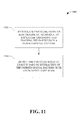
- FIG. 11 illustrates a representative flow diagram of a methodology that can facilitate electronically manipulating and detecting small scale particles in accordance with an aspect of the disclosed subject matter.
- FIG. 12 illustrates a representative flow diagram of a methodology that can apply voltage waveforms at desired frequencies to facilitate electronically manipulating and detecting small scale particles in accordance with an aspect of the disclosed subject matter.
- FIG. 13 depicts a representative flow diagram of a methodology that can facilitate electronically manipulating and detecting small scale particles via sequentially applying multiple frequencies in accordance with an aspect of the disclosed subject matter.
- FIG. 14 depicts a representative flow diagram of a methodology that can facilitate detecting small scale particles in accordance with an aspect of the disclosed subject matter.
- FIG. 15 illustrates the velocity profiles of a plurality of example particles in response to dielectrophoresis (DEP) and time multiplexed or traveling-wave DEP (TWDEP), showing the differences in velocity that occur as a result of their relative differences in electrical properties.
- DEP dielectrophoresis
- TWDEP traveling-wave DEP
- FIGS. 16A-E illustrate an example method of separating two disparate particle types via multiplexed DEP techniques in accordance with the subject innovation.
- FIG. 17 illustrates comparison of TWDEP and DEP velocities for models of live and dead yeast cells in a 5 mS/m buffer solution with model parameters for cells extracted from best-fit analysis of experimental data.
- FIGS. 18A-B illustrate close-up views of the DEP and TWDEP velocities for live and dead yeast cells, evaluated at frequencies selected from techniques described herein.
- FIG. 19B illustrates average net TWDEP velocity on live and dead yeast cells when multiplexing between these two configurations as a function of the duty cycle.
- FIG. 21 illustrates a method of fractionation of a sample containing four particle types by repeated application of the separation method discussed in connection with FIGS. 16A-E .
- small scale particles in this context refers generally to objects with dimensions equal to or smaller than 1-100 ⁇ m, (e.g., biological cells) and particularly to objects with dimensions of nanometer scale and below (e.g., viruses, components of viruses, and biological macromolecules.
- At least a portion of the handle silicon can be removed (e.g., by grinding or other process) from the IC chip so that the active semiconductor layers (e.g., doped silicon or polysilicon) of the chip can be exposed or at least can be closer to the face-up surface of the chip.
- a plurality of electrodes can be formed on one or more of the active semiconductor layers, which can support the formation of features (e.g., electrode size and electrode-to-electrode separation) at the smallest, or at least a significantly smaller, available dimension (e.g., nanometer scale in size) of an IC fabrication process to facilitate manipulation of small scale particles.
- the plurality of electrodes can be formed as a large and dense collection of electrodes.
- the subject innovation by forming a large and dense collection of electrodes (e.g., linear electrode array, two-dimensional electrode array, etc.) with such a fine pitch, can yield a high degree of selectivity when manipulating submicron scale particles.
- This is a large reduction in electrode feature size as compared to conventional DEP-based systems and devices implemented using integrated circuit technologies, which typically form trapping electrodes using the top metal layers of an IC chip that are normally reserved for bonding pads and are typically on a scale ranging from a few microns to tens of microns.
- a lab-on-chip device can comprise the IC chip with the plurality of electrodes and the fluidic chamber(s).
- the lab-on-chip device can also comprise digital and/or analog electronic components that can facilitate controlling and selecting desired voltage waveforms that can be applied to the electrodes.
- the digital and/or analog electronic components can be on the same IC chip as the electrodes.
- the digital and/or analog electronic components can be on one or more disparate IC chips of a lab-on-chip device (e.g., 3D integrated circuit), which can comprise a desired number of IC chips (e.g., IC wafers) positioned in a vertically tiered manner, for example.
- the lab-on-chip can be employed to facilitate efficient manipulation and detection of small scale particles, which can be contained in a buffer solution in the fluidic chamber(s).
- Embodiments of the subject innovation can reduce both the time and cost for the fractionation and assay of bio-mixtures. Turnaround time can be reduced from hours to minutes. This can enable researchers to process samples non-destructively, and assay results in a faster—test, analyze, evaluate—cycle. This will allow more efficient exploration of a wider range of sample points in many experiments.
- the ability to fractionate mixed samples with a high degree of separation sensitivity means that species with small changes in morphology, surface coatings, and even interior chemistry can be accurately sorted. This can provide a means of understanding the relationship between these differences and the biological characteristics of these particles, which can help drive new advances in microbiology research.
- systems and methods of the subject innovation can serve as the basis for a new class of portable diagnostic equipment.
- Multiplexed field configurations can vary in frequency, amplitude, and direction of the phase gradient and each can be optimized to apply maximal force to a specific particle type. When applied in sequence they can be configured to generate a different net force on each particle type of interest. Moreover, by exploiting the size of the electrode array and creating spatially non-uniform configurations within the multiplexed sequence, the device can be programmed to separate, isolate, and hold in position specific particle types that would otherwise be indistinguishable using conventional methods.
- FIG. 1 illustrates a diagram of a device 100 that can facilitate electronic manipulation and detection of small scale particles in accordance with an aspect of the disclosed subject matter.
- the device 100 can include an IC chip 102 that can comprise a plurality of electrodes 104 that can be formed in a pattern (e.g., a linear array, 2-dimensional or other regular pattern, or an irregular pattern).
- the plurality of electrodes 104 can be used to facilitate electronic manipulation (e.g., employing DEP) of one or more disparate types of particles (e.g., submicron scale particles, such as nanometer scale particles) that can be contained in a buffer solution that can be inserted into a fluidic chamber(s) 106 (e.g., microfluidic structure(s), channel(s), trench(es) and/or reservoir(s))) formed (e.g., etched) in a fluid containment structure 108 , which can be located on the top surface of the device 100 .
- a fluidic chamber(s) 106 e.g., microfluidic structure(s), channel(s), trench(es) and/or reservoir(s)
- a fluid containment structure 108 e.g., etched
- the fluid containment structure(s) 108 can be formed by removing any or all of the handle silicon (e.g., substrate) from the IC chip 102 .
- a portion of the handle silicon of the IC chip 102 can be removed (e.g., employing chemical etching techniques) to form the fluidic chamber(s) 106 , where the remaining handle silicon can be the fluid containment structure 108 .
- all or a portion of the handle silicon can be removed from the IC chip 102 , and a fluid containment structure 108 can be formed by depositing virtually any of a variety of materials that can be grown on, deposited on, or attached to the surface of the IC chip 102 . It is to be appreciated and understood that removal of all or a portion of the handle silicon typically can occur in relation to orienting the IC chip 102 so that the metal layer of the IC chip is face down, such as described herein.
- the IC chip 102 can be oriented so that the handle silicon of the IC chip 102 can be face up, where the face-down surface (e.g., the metal interconnection layer(s)) of the IC chip 102 can be fastened (e.g., bonded) to a support structure (e.g., circuit board, packaging device, ceramic interposer, ceramic interposer, another IC chip as part of a vertical chip stack, . . . —not shown) thereunder.
- a support structure e.g., circuit board, packaging device, ceramic interposer, ceramic interposer, another IC chip as part of a vertical chip stack, . . . —not shown
- At least a portion (e.g., part or all) of the handle silicon can be removed (e.g., removed by grinding) so that the active semiconductor layer(s) 110 can be exposed or at least can be closer to the surface of the IC chip 102 , as compared to conventional devices (e.g., lab-on-chip devices).
- the active semiconductor layer(s) 110 can be the layer(s) of IC chip 102 that can maintain the smallest feature size (or at least a very small feature size) on the IC chip 102 (e.g., components and vias formed on the active semiconductor layer(s) 110 can have the smallest feature size or a substantially smaller feature size as compared to other layers, such as metal layers, of the IC chip 102 ).
- a plurality of electrodes 104 can be formed in the active semiconductor layer(s) layer 110 , where each of the plurality of electrodes 104 can be formed having a size corresponding to the smallest (or a very small) feature size for the active semiconductor layer(s) 110 of the IC chip 102 .
- each of the plurality of electrodes 104 can be submicron scale (e.g., nanometer scale) in size (e.g., 180 nm width, 65 nm width, or smaller).
- the plurality of electrodes 104 e.g., 2,048 electrodes, or less or more
- the gap spacing between adjacent electrodes 104 in the array can be on a submicron scale (e.g., 270 nm or smaller gap spacing) to facilitate electronic manipulation of particles.
- the plurality of electrodes 104 can be positioned in close proximity to one or more fluidic chambers 106 (e.g., trench(es)) that can be formed (e.g., etched) in the fluid containment structure 108 (e.g., top surface of the device 100 ).
- the fluid containment structure 108 can be fashioned on the face-up surface of the IC chip 102 , where the fluidic chamber(s) 106 can be positioned over the plurality of electrodes 104 .
- the plurality of electrodes 104 can be positioned in close proximity to the fluidic chamber(s) 106 .
- the fluidic chamber(s) 106 can have a bottom surface that can be constructed of a reflective material or can have a reflective material placed or formed thereon.
- the reflective bottom surface of the fluidic chamber(s) 106 can facilitate detection (e.g., optical detection) of particles in the buffer solution (e.g., after manipulation of the particles).
- fluidic chambers 106 can be the same or different in size, as desired.
- One or more fluidic chambers 106 can be utilized for other desired purposes, such as, for example, using a fluidic chamber(s) 106 as a reservoir that contains a relatively large quantity particles contained in a buffer solution, where a desired portion of the particles and buffer solution can be distributed to another fluidic chamber 106 positioned in close proximity to the electrodes 104 .
- the device 100 can be utilized to facilitate manipulating small scale particles, such as submicron scale particles.
- a desired buffer solution can be inserted into the fluidic chamber(s) 106 , where there can be particles of interest (e.g., submicron scale particles, such as nanometer scale particles) contained in the buffer solution.
- particles of interest e.g., submicron scale particles, such as nanometer scale particles
- an electrokinetic technique such as, for example, EP, DEP, MFDEP, and/or MDEP, can be employed to facilitate arranging particles into a defined spatial pattern.
- Specified voltage waveforms can be applied to a subset(s) of the electrodes 104 to facilitate generating a spatially non-uniform electric field(s) having one or more specified frequency(ies) that can be utilized to apply a corresponding force on the particles of interest, which can be one or more disparate types of particles, to manipulate (e.g., move particles, sort disparate types of particles, separate disparate types of particles) and trap the particles without having to come in direct contact with the particles.
- Electrodes 104 in close proximity to the fluidic chamber(s) 106 can facilitate optimizing (e.g., maximizing) the electric field strength(s), which can facilitate electronic manipulation (e.g., DEP) and detection of submicron particles contained in the buffer solution in the fluidic chamber(s) 106 .
- optimizing e.g., maximizing
- the electric field strength(s) can facilitate electronic manipulation (e.g., DEP) and detection of submicron particles contained in the buffer solution in the fluidic chamber(s) 106 .
- device 100 can comprise one or more covers (not shown) that can be placed on the one or more fluidic chambers 106 , as desired, to cover the opening of a fluidic chamber(s) 106 to facilitate improving the strength of an electric field generated and applied to particles in the fluidic chamber(s) 106 .
- the cover(s) can comprise a planar electrode(s) (not shown) that can facilitate providing an even ground plane.
- the cover can modify an electric field so that the electric field can be between adjacent electrodes 104 and the planar electrode, which can improve the electric field strength in the fluidic chamber(s) 106 , as opposed to the resulting electric field between adjacent electrodes 104 when no cover is employed.
- a cover(s) can comprise a plurality of planar electrodes that can be formed into a desired defined pattern (e.g., linear array, two dimensional array, regular pattern, irregular pattern), which can further improve electric field strength and control of manipulation of particles.
- a desired defined pattern e.g., linear array, two dimensional array, regular pattern, irregular pattern
- the voltage waveforms provided to the electrodes 104 can be from electronic components (not shown) on IC chip 102 , one or more other IC chips (not shown in FIG. 1 ) with components formed thereon to facilitate providing the voltage waveforms to the electrodes 104 , an integrated circuit on a printed circuit board(s) (not shown in FIG. 1 ) with components contained thereon to facilitate providing the voltage waveforms to the electrodes 104 , and/or other components that can facilitate providing the voltage waveforms to the electrodes 104 .
- the device 100 can arrange and trap particles in the form of a defined spatial pattern to facilitate detection and assay of the one or more types of particles, where respective particles can be arranged based at least in part on the respective physical properties, such as size, mass, and dielectric properties (e.g., permittivities, conductivities), of the particles.
- respective particles can be arranged based at least in part on the respective physical properties, such as size, mass, and dielectric properties (e.g., permittivities, conductivities), of the particles.
- there can be a mixture of particles comprising a first type of particle and a second type of particle.
- the mixture of particles can be placed in a buffer solution, where the buffer solution can be placed in a fluidic chamber 106 of device 100 .
- the first type of particle can have a first set of physical properties
- the second type of particle can have a second set of physical properties.
- a first subset of electrodes 104 can receive a first voltage waveform (e.g., sine wave) at a first frequency and first magnitude, and a first electric field (e.g., first spatially non-uniform electric field) can be generated and applied to the particles in the fluidic chamber 106 .
- a second subset of electrodes 104 can receive a second voltage waveform at a second frequency and second magnitude, and a second electric field (e.g., second spatially non-uniform electric field) can be generated and applied to the particles in the fluidic chamber 106 .
- the first type of particles can be attracted to the first subset of electrodes 104 .
- the first type of particles can move to a region in the fluidic chamber 106 near the first subset of electrodes 104 and can become trapped as the first type of particles can be attracted to the electric-field maxima associated with the first electric field, while the second type of particles can move away from the region in the fluidic chamber 106 near the first subset of electrodes 104 .
- the second type of particles can be attracted to the second subset of electrodes 104 .
- the second type of particles can move to a region in the fluidic chamber 106 near the second subset of electrodes 104 and can become trapped as the second type of particles can be attracted to the electric-field maxima associated with the second electric field.
- device 100 can facilitate manipulation of more than two types of particles as desired.
- the device 100 can be utilized to employ sequential application of multiple frequencies (e.g., in temporal and/or spatial sequences) to facilitate manipulating disparate types of particles to arrange and trap the particles as desired.
- disparate types of particles can be contained in a buffer solution placed in a fluidic chamber 106 .
- a first voltage waveform having a first frequency can be applied to a first subset of electrodes 104 to generate a first electric field (e.g., first spatially non-uniform electric field).
- a first force based at least in part on the first electric field, can be applied to the disparate types of particles where at least a first subset of particles can be manipulated so they are separated from other particles and trapped in a region of the fluidic chamber 106 near the first subset of electrodes 104 based at least in part on the first frequency and the physical properties of the first subset of particles (e.g., the first subset of particles can form a diffraction line that can correspond to the layout of the first subset of electrodes 104 ).
- a second voltage waveform having a second frequency can be selected and applied to a second subset of electrodes 104 to facilitate manipulating a second subset of particles to separate them from other particles and trap the second subset of particles in a region in the fluidic chamber 106 near the second subset of electrodes.
- one or more additional voltage waveforms of respective frequencies can be applied to one or more additional subsets of electrodes 104 to facilitate manipulating the particles so the particles in the fluidic chamber 106 can be separated and arranged into a desired spatial pattern based at least in part on the frequencies applied and respective physical properties of the particles.
- the bifurcation process can continue until the particles are separated and arranged into a desired spatial pattern to facilitate detection of the particles.
- the particles can be arranged into a diffraction grating, where there can be one or more grating lines for each type of particle (e.g., one or more grating lines for a first type of particle, one or more grating lines that contain a second type of particle, etc.).
- a diffraction grating can facilitate detecting and assaying the respective particles.
- FIGS. 2A-2D illustrated is an example of employing DEP to facilitate electronic manipulation of disparate types of particles (e.g., herpes simplex virus-1 (HSV-1) capsids).
- FIG. 2A is an illustrative diagram of an example portion of a fluidic chamber 106 that can contain disparate types of particles contained in a buffer solution in the fluidic chamber 106 .
- the disparate particles can be randomly positioned in the buffer solution in the fluidic chamber 106 prior to the electronic manipulation being performed.
- the subject innovation is not limited to manipulating and separating five particle types, as the subject innovation can facilitate manipulating and separating less than five disparate types of particles, five disparate types of particles, or more than five disparate types of particles, as desired.
- FIG. 2B depicts an illustrative diagram of the example portion of the fluidic chamber 106 with the disparate types of particles in the buffer solution when a first voltage waveform having a first frequency is applied to a first subset of electrodes 104 to facilitate manipulating the particles.
- FIG. 2C depicts an illustrative diagram of the example portion of the fluidic chamber 106 with the disparate types of particles in the buffer solution when a second voltage waveform having a second frequency is sequentially applied to a second subset of electrodes 104 to facilitate further manipulating the particles.
- the second voltage waveform with the second frequency can be applied to the second subset of electrodes 104 which can generate a second electric field (e.g., spatially non-uniform electric field) where the force of the second electric field (and the first electric field) can facilitate trapping two types of disparate particles 202 and 204 based at least in part on the second frequency and the respective physical properties of particles 202 and 204 (e.g., particle 202 can have a conductivity of 33.0e-3 Sm ⁇ 1 , and particle 204 can have a conductivity of 31.5e-3 Sm ⁇ 1 ), and the remaining disparate particles 206 , 208 , and 210 can move to local minima on the right, as depicted at reference numerals 214 , 216 and 218 , respectively.
- a second electric field e.g., spatially non-uniform electric field
- FIG. 2D depicts an illustrative diagram of the example portion of the fluidic chamber 106 with the disparate types of particles in the buffer solution after five voltage waveforms having five respective frequencies are sequentially applied to respective subsets of electrodes 104 to facilitate further manipulating and trapping the particles.
- a third voltage waveform with the third frequency can be applied to a third subset of electrodes 104 which can generate a third electric field (e.g., spatially non-uniform electric field) where the force of the third electric field can attract and trap particles 206 based at least in part on the third frequency and the physical properties of particles 206 (e.g., particle 206 can have a conductivity that is lower than the particles 202 and 204 ), and the remaining disparate particles 208 and 210 can move to local minima on the right.
- a third electric field e.g., spatially non-uniform electric field
- a fourth voltage waveform with the fourth frequency can be applied to a fourth subset of electrodes 104 which can generate a fourth electric field (e.g., spatially non-uniform electric field) where the force of the fourth electric field can attract and trap particles 208 based at least in part on the fourth frequency and the physical properties of particles 208 (e.g., particle 208 can have a conductivity that is lower than the particles 202 , 204 , and 206 ), and the remaining particles 210 can move to local minima on the right.
- a fifth voltage waveform with the fifth frequency e.g., higher than the fourth frequency
- can be applied to a fifth subset of electrodes 104 (not shown in FIG.
- a fifth electric field e.g., spatially non-uniform electric field
- the force of the fifth electric field can attract and trap particles 210 based at least in part on the fifth frequency and the physical properties of particles 210 (e.g., particle 210 can have a conductivity that is lower than the particles 202 , 204 , 206 , and 208 ).
- the result can be fully fractionated mixture in five DEP traps, where the particles 202 , 204 , 206 , 208 , and 210 can be fractionated in order of decreasing conductivity, as depicted at reference numerals 220 , 222 , 224 , 226 , and 228 , respectively.
- the subject innovation is not so limited, as there can be more than one line dedicated to a particular type of particle.
- the particles 202 , 204 , 206 , 208 , and 210 can be manipulated (e.g., using device 100 ) so that there can be more than one line of particles 202 , more than one line of particles 204 , more than one line of particles 206 , more than one line of particles 208 , and/or more than one line of particles 210 , as desired.
- particles can be formed into virtually any desired spatial pattern.
- particles can be manipulated into a linear pattern, such as a diffraction grating, a two-dimensional pattern or other regular pattern, an irregular or a non-uniform pattern.
- device 100 can be utilized to employ multiple frequencies at the same time to facilitate manipulating particles contained in a buffer solution in a fluidic chamber 106 based at least in part on the respective frequencies and the respective physical properties of the particles.
- one voltage waveform having a first frequency can be applied to a first subset of electrodes 104 and a second voltage waveform having a second frequency can be applied to a second subset of electrodes 104 at the same time to facilitate manipulating the particles based at least in part on the first and second frequencies and the respective physical properties (e.g., electrical conductivity) of the particles.
- Device 300 can include an IC chip 102 (e.g., also referred to as third IC chip 102 with regard to device 300 ) on which a plurality of electrodes 104 can be formed.
- IC chip 102 e.g., also referred to as third IC chip 102 with regard to device 300
- a fluid containment structure 108 can be placed over the plurality of electrodes 104 and IC chip 102 .
- a fluidic chamber(s) 106 can be formed in the fluid containment structure 108 , where the fluidic chamber(s) 106 can be formed over the plurality of electrodes 104 .
- the IC chip 102 , plurality of electrodes 104 , fluidic chamber(s) 106 , and fluid containment structure 108 each can be the same or similar as, and/or can comprise the same or similar functionality as, respective components such as more fully described herein, for example, with regard to device 100 .
- a second IC chip 306 can comprise a plurality of selector components 308 formed thereon that can be used to facilitate selecting a desired waveform of a predefined number of different voltage waveforms that can be applied to corresponding electrodes 104 to facilitate manipulating particles (e.g., particles in a buffer solution in a fluid channel(s) 106 ).
- the voltage waveforms can be provided to the selector components 308 externally or the voltage waveforms can be generated by device 300 .
- the orientation of the second silicon wafer 306 optionally can be re-arranged such that the handle silicon region of the second IC chip 306 can be face up and the surface where the metal interconnection layers are located can be face down (e.g., second IC chip 306 can be turned upside down), as compared to conventional orientation of IC chips, and the second IC chip 306 can be adhered (e.g., bonded) to the top surface of the first IC chip 302 , where the second IC chip 306 is positioned above the first IC chip 302 in the vertical chip stack.
- at least a portion of the handle silicon can be removed from the second silicon wafer 306 .
- the third IC chip 102 can be oriented so that the handle silicon region of the IC chip 102 can be facing up, and the face-down surface (e.g., having metal interconnection layers) of the third IC chip 102 can be adhered to the second IC chip 304 in the vertical chip stack.
- the active semiconductor layers 110 of the third IC chip 102 which can comprise the plurality of electrodes 104 , can be in closer proximity to the fluidic chamber(s) 106 of the fluid containment structure 108 , which can be adhered to the third IC chip 102 in the vertical chip stack.
- the device 300 can be utilized to facilitate manipulating (e.g., employing EP, DEP, MDEP, and/or MFDEP) small scale particles (e.g., one or more disparate types of particles), such as submicron scale particles (e.g., nanometer scale particles).
- a desired buffer solution can be inserted into the fluidic chamber(s) 106 , where there can be particles of interest (e.g., submicron scale particles, such as nanometer scale particles) contained in the buffer solution.
- the device 300 can be placed in circulation mode where a subset of control components 304 can provide signals to corresponding subset of selector components 308 to facilitate producing a time sequence pattern for applying the voltage waveforms to a corresponding subset of electrodes 104 .
- the specified voltage waveforms applied to the desired electrodes 104 in the time sequence pattern can facilitate generating one or more spatially non-uniform electric fields that can be utilized to apply one or more forces, which can correspond to the one or more respective electric fields, on the particles of interest to manipulate and trap the particles, or a subset thereof, without having to come in direct contact with the particles.
- Electrodes 104 in close proximity to the fluidic chamber(s) 106 , along with the submicron scale of the electrodes 104 (e.g., 180 nm or smaller width) and submicron scale of the gap spacing (e.g., 270 nm or smaller gap spacing) between adjacent electrodes 104 in the linear electrode array, can facilitate optimizing (e.g., maximizing) the electric field strength, which can facilitate electronic manipulation and detection of submicron particles contained in the buffer solution in the fluidic chamber(s) 106 .
- optimizing e.g., maximizing
- the trapped particles can be detected, for example, using innovative macro-scale optical detection, such as more fully described herein (e.g., system 1100 , methodology 1500 ).
- device 300 can be a three-dimensional chip stack that can be comprised of the fluid containment structure 108 , the third IC chip 102 (e.g., third tier), the second IC chip 306 (e.g., second tier), and the first IC chip 302 (e.g., first tier), wherein the topmost tier, the third IC chip 102 , can comprise an active semiconductor layer(s) 110 with an array of electrodes 104 formed thereon.
- the voltage (e.g., voltage waveforms) on each electrode 104 can be individually driven by analog circuitry (e.g., selector components 308 ) contained in the second IC chip 306 .
- the first IC chip 302 can include a plurality of control components 304 (e.g., digital circuits comprising circular shift registers) that can send signals to corresponding selector components 308 to facilitate selecting a desired voltage waveform for each electrode 104 at a desired time.
- control components 304 e.g., digital circuits comprising circular shift registers
- two pad cuts can be made through the fluid containment structure 108 (e.g., over-glass layer), located on the surface of the chip.
- the areas of top level metal, which normally are used for contact pads can be etched (e.g., chemically etched) away within this region to form trenches, which can be fluidic chamber(s) 106 .
- the fluidic chamber(s) 106 can be utilized to hold a buffer solution that contains particles of interest (e.g., submicron scale particles, such as certain viruses).
- the active semiconductor layer(s) 110 comprising the plurality of electrodes 104 can be located in very close proximity to the fluidic chamber(s) 106 .
- the active semiconductor layer(s) 110 of the third IC chip 102 can be used to create efficient DEP trapping electrodes (e.g., electrodes 104 ).
- the active semiconductor layer(s) is used as interconnect for active circuit devices because the active semiconductor layer(s) would be at the bottom region of the IC chip.
- the plurality of electrodes 104 can comprise a large number (e.g., 2,048, or more or less) electrodes (e.g., DEP electrodes), formed in a linear array on the active semiconductor layer 110 (e.g., polysilicon layer) of the IC chip 102 .
- each of the electrodes 104 can be 180 nm wide (or smaller) and 200 ⁇ m long, where the plurality of electrodes 104 can be situated under the fluidic chamber area (e.g., trench area) with a center to center pitch of 450 nm and an electrode gap spacing of 270 nm (or smaller).
- the plurality of electrodes 104 can be separated from the bottom surface of the fluidic chamber(s) 106 by 650 nm of oxide (not shown).
- the first IC chip 302 can comprise a plurality of control components 304 , where each control component 304 can comprise a control register for each of the 2,048 electrodes.
- Each control register can be utilized to facilitate selecting among four source waveforms (e.g., voltage waveforms) that can be provided to the device 300 from an external source or can be provided by the device 300 .
- the control components 304 which can comprise digital circuitry, can facilitate controlling corresponding selector components 308 of the second IC chip 306 , where the selector components 308 can comprise analog circuitry.
- each selector component 308 which can be an analog mux (e.g., 4:1 analog mux)
- a corresponding control component 304 which can be, e.g., a 2-bit wide, 4-bit deep circular shift register, although others can also be used.
- the shift registers can have two modes, load and circulate. To facilitate minimizing the number of input/output (I/O) pins necessary for loading, the output of the last shift register in each row of shift registers can be fed to the input of the subsequent row of shift registers.
- the signal on an electrode 104 can switch between one of a plurality (four, for the example given) of analog inputs on each clock cycle.
- the subject innovation provides desirable flexibility for post-fabrication modification and/or experimentation, as the voltage waveforms are not limited to voltage waveforms generated on the device 300 , as other external voltage waveforms can be supplied to the device 300 , as desired.
- device 300 is described with regard to three tiers (e.g., third IC chip 102 , second IC chip 306 , and first IC chip 302 ) in the vertical chip stack, the subject innovation is not so limited as there can be virtually any number of IC chips employed in accordance with the disclosed subject matter.
- device 300 can comprise less than three IC chips, three IC chips, or more than three IC chips, as desired.
- FIG. 4 illustrates a diagram of an example device 400 that can facilitate electronic manipulation and detection of small scale particles in accordance with an embodiment of the disclosed subject matter.
- Device 400 can comprise a IC chip 102 (e.g., also referred to as third IC chip 102 ) that can contain a plurality of electrodes 104 , a fluidic chamber(s) 106 , a fluid containment structure 108 , an active semiconductor layer(s) 110 , a first IC chip 302 , a plurality of control components 304 , a second IC chip 304 , and a plurality of selector components 308 .
- IC chip 102 e.g., also referred to as third IC chip 102
- third IC chip 102 can contain a plurality of electrodes 104 , a fluidic chamber(s) 106 , a fluid containment structure 108 , an active semiconductor layer(s) 110 , a first IC chip 302 , a plurality of control components 304
- the IC chip 102 , plurality of electrodes 104 , fluidic chamber(s) 106 , fluid containment structure 108 , active semiconductor layer(s) 110 , first IC chip 302 , plurality of control components 304 , second IC chip 304 , and plurality of selector components 308 each can be the same or similar as, and/or can comprise the same or similar structure and/or functionality as, respective components such as more fully described herein, for example, with regard to device 100 and/or device 300 .
- the IC chips 102 , 302 , and 306 each can be of a size on the order of single millimeters, e.g., 4 mm in length and 2 mm in width (or other dimensions).
- the fluid chamber 106 can be 1000 ⁇ m in length and 200 ⁇ m in width.
- the gap spacing between adjacent electrodes 104 in the linear electrode array of such an example can be 270 nm. It is to be appreciated and understood that the aforementioned dimensions are examples, and the subject innovation is not so limited, as, in accordance with various embodiments, the respective dimensions can be smaller than or larger than the aforementioned dimensions.
- FIG. 5 depicts an example block diagram of a system 500 that can facilitate providing a desired voltage waveform to an electrode(s) associated with a lab-on-chip in accordance with an embodiment of the disclosed subject matter.
- System 500 can include a control component 304 that can comprise a predetermined number of flip-flop components 502 that can be connected together to form a circular shift register (although specific numbers of components are illustrated, it is to be understood that those numbers can vary).
- the number of flip-flop components 502 employed can be based at least in part on the number of voltage waveforms that can be applied to an associated electrode 104 (e.g., four flip-flop components 502 to facilitate selecting between four voltage waveforms).
- the control component 304 also can include a mux component 504 (e.g., analog mux) that can facilitate selecting between a load mode and circulate mode.
- the control component 304 can be connected to the selector inputs of a selector component 308 , which can be connected to an electrode 104 connected thereto.
- the selector component 308 can receive as input a predetermined number of voltage waveforms, where one of the voltage waveforms can be selected and provided as an output to the electrode 104 based at least in part on the signals received at the selector inputs of the selector component 308 .
- the voltage waveforms can be received from another component of a lab-on-chip associated therewith or an external component, as desired.
- the output of the control component 304 can be provided to the input of another control component 304 (e.g., input of a shift register of control component 304 ) (not shown) on a successive row of control components 304 (not shown) when initializing a selection pattern for the voltage waveforms.
- FIG. 6 is a diagram that illustrates example results 600 of a 2D finite-element analysis of the electric field generated within the fluidic trench (e.g., 106 ) by the electrodes and the resultant dielectrophoretic forces that act on the particles.
- the first five electrodes starting from the left hand side of FIG. 6 , are assigned a magnitude of 1.5V.
- the voltages on the remaining electrodes, on the right hand side of FIG. 6 are set 180° out of phase with respect to the other electrodes. This creates an electric field maximum between the 5th and 6th electrode.
- the arrows in FIG. 6 show the direction of the dielectrophoretic forces that act on the particles as a function of their location within the trench.
- the particles are more polarizable than their surrounding medium, yielding a positive value for Re[K cm ] (i.e., the real part of the Clausius-Mossotti factor, discussed further herein) and the particles within the buffer solution are attracted towards the electric-field maxima.
- Re[K cm ] i.e., the real part of the Clausius-Mossotti factor, discussed further herein
- Experimental results show that when HSV virions are placed in a mannitol solution with a conductivity of 5 mSm ⁇ 1 , the particles will transition from undergoing positive to negative DEP in the frequency in the range of 4-5 MHz.
- FIGS. 7A through 7D illustrate the results of a simulation of electronic manipulation of virions (e.g., particles) in a fluidic chamber (e.g., fluidic chamber 106 ), where a large concentration of virions are randomly placed in a 4 ⁇ m ⁇ 25 ⁇ m area of the fluidic trench.
- the voltages are set such that each electrode (e.g., 104 ) is 180° out of phase with respect to its two neighboring electrodes, creating an alternating pattern of electric field minima and maxima along the bottom surface of the fluidic trench.
- the subject innovation can facilitate detecting small scale particles (e.g., submicron particles) using innovative macro-scale optical detection systems, devices, and methodologies.
- the IC chip 102 , plurality of electrodes 104 , fluidic chamber(s) 106 , fluid containment structure 108 each can be the same or similar as, and/or can comprise the same or similar structure and/or functionality as, respective components such as more fully described herein, for example, with regard to device 100 , device 300 , and device 400 .
- the orientation of the IC chip 102 (e.g., turned upside down so that the active semiconductor layer(s) 110 can be closer to the fluidic chamber(s) 106 , and the metal interconnection layers are face down) and removal of at least a portion of the handle silicon from the third IC chip 102 can facilitate placing the plurality of electrodes 104 closer to the surface of the IC chip 102 and fluidic chamber(s) 106 and/or can facilitate creating the fluid containment structure 108 , which can be formed of the handle silicon, as desired, in accordance with an embodiment.
- the bottom surface of the fluidic chamber(s) 106 can be structured so that it is reflective (e.g., a reflective material can be formed, deposited, or coated on at least a portion of the surface of the fluidic chamber(s) 106 ).
- the detector component 1008 also can measure optical power of diffracted light at an angle that corresponds to the selected diffraction order for the diffraction grating, or portion thereof (e.g., I( ⁇ ) as described with regard to FIG. 8 and Equation 2).
- the detector component 1008 e.g., one or more detectors
- the optical power of diffracted light at the detection angle can depend on the optical power at the readout wavelength of the incident light beam, the diffraction order selected, and the efficiency of the diffraction grating.
- the light source component 1006 can apply an incident light beam to a defined spatial pattern comprising particles, where the defined spatial pattern can be an irregular or a non-uniform pattern.
- the interaction between the incident light beam and the defined spatial pattern can result in an image being formed, which can be detected by the detector component 1008 .
- the image can be in the form of a hologram, for example.
- system 1000 can efficiently electronically manipulate particles to arrange particles in a desired manner, and can employ a particle detector component 1004 that can employ macro-scale optical detection of particles to facilitate detecting and assaying particles of interest in the buffer solution.
- particles can be manipulated, using an electrokinetic technique, to facilitate arranging and trapping the particles in a defined spatial pattern based at least in part on respective physical properties of respective particles (e.g., size, mass, electrical conductivity, . . . ) and at least one non-uniform electric field applied to the particles by a subset(s) of electrodes 104 .
- the particles can be contained in a buffer solution in a fluidic chamber(s) 106 that can be in close proximity to a plurality of electrodes 104 .
- the at least one non-uniform electric field can be generated as a function of at least one voltage waveform of at least one specified frequency applied to the subset(s) of electrodes, wherein the particles and the subset(s) of electrodes can be submicron in scale.
- the particles can be manipulated to arrange, sort, and/or trap particles in a desired spatial pattern, such as a diffraction grating, based at least in part on respective physical properties of respective particles and one or more non-uniform electric fields that can be applied to the particles by a subset(s) of electrodes 104 .
- the particles e.g., submicron scale particles
- a subset(s) of electrodes 104 can receive a voltage waveform(s) having a desired frequency(ies), which can cause the subset(s) of electrodes 104 to provide a respective spatially non-uniform electric field(s) that can manipulate and trap the particles, or subset thereof, based at least in part on the respective physical properties of the particles.
- the particles can be detected based at least in part on interaction of the defined spatial pattern with an incident light beam. For instance, when the particles are arranged to form a diffraction grating, the particles can be detected based at least in part on the wavelength of a light beam applied to at least a portion of the diffraction grating and characteristics (e.g., diffraction angle, optical power) of light diffracted from the at least a portion of the diffraction grating.
- a light beam e.g., visible or subvisible light
- a desired wavelength can be applied to at least a portion of the diffraction angle of particles (e.g., diffraction grating).
- the diffraction angle can be determined based in part on the wavelength of the applied light, the distance between adjacent grating lines of particles, and the diffraction order selected (e.g., as selected by a user).
- the optical power at the diffraction angle can be measured and can be dependent on optical power at the readout wavelength of the applied light, the diffraction order selected, and efficiency of the diffraction grating.
- the detected or measured characteristics of the light diffracted from the diffraction grating, or portion thereof can be calibrated against known particle assays to obtain accurate measurements of particle populations in the diffraction grating, or portion thereof to facilitate detection and assay of particles of interest in the buffer solution.
- submicron scale particles can be detected and assayed employing innovative macro-scale optical detection.
- methodology 1100 can end.
- a methodology 1200 that can apply a desired number of voltage waveforms at desired frequencies to facilitate electronically manipulating and detecting small scale particles in accordance with an aspect of the disclosed subject matter.
- a buffer solution that can contain particles of interest (e.g., one or more disparate types of submicron scale particles) can be inserted into a fluidic chamber(s) 106 .
- a particle manipulation device e.g., device 100 , device 300 , device 400
- a lab-on-chip can comprise one or more fluidic chambers 106 formed in a fluid containment structure 108 of the particle manipulation device.
- the particle manipulation device can be formed so that electrodes 104 , which can be contained on an active semiconductor layer(s) 110 of an IC chip 102 , where the active semiconductor layer(s) 110 can be positioned directly under the fluid containment structure 108 .
- the IC chip 102 can be oriented so that its handle silicon region can be face up and its metal interconnect layers can be face down.
- the IC chip 102 can have at least a portion of its handle silicon removed so that the active semiconductor layer(s) 110 can be exposed or at least closer to the face-up surface of the IC chip 102 , so the electrodes 104 formed thereon can be placed in close proximity to the fluidic chamber(s) 106 in the fluid containment structure 108 to facilitate electronic manipulation (e.g., employing DEP) and detection of particles contained in the buffer solution.
- electronic manipulation e.g., employing DEP
- the electrodes 104 can be formed so that they are submicron in size (e.g., width of 180 nm or smaller) and the gap spacing between adjacent electrodes 104 , which can be formed in a linear electrode array, can be submicron in size (e.g., gap spacing can be 270 nm or smaller).
- At 1204 at least one desired electric field (e.g., spatially non-uniform electric field(s)) can be generated.
- the particle manipulation device can generate one or more desired electric fields to facilitate manipulating (e.g., moving and arranging) the particles.
- the particle manipulation device can comprise a plurality of selector components (e.g., 308 ) that can be connected to corresponding electrodes 104 to facilitate providing a selected voltage waveform(s), where each waveform can have a respective desired frequency, to a subset(s) of electrodes 104 at each clock cycle.
- the selector components can be connected to corresponding control components (e.g., 304 ), which can facilitate controlling selection of the voltage waveforms on the rising edge of each clock cycle.
- the voltage waveforms can be external voltage waveforms and/or voltage waveforms generated by the particle manipulation device.
- the selected voltage waveforms can be provided to the subset(s) of electrodes 104 to facilitate generating the desired electric field(s) in order to facilitate manipulating the particles in the buffer solution in the fluidic chamber(s) 106 .
- more than one voltage waveform having a respective frequency can be applied to respective subset of electrodes 104 to facilitate manipulating the particles to sort and arrange different types of particles so particles of the same type can be grouped together in a region of a desired spatial pattern, for example, in one or more lines (e.g., parallel or substantially parallel lines) of a diffraction grating.
- the multiple voltage waveforms (having respective frequencies) can be applied sequentially or can be applied at the same time, as desired.
- the at least one generated electric field can be applied to the particles.
- the desired electric field(s) e.g., spatially non-uniform electric field
- the electrodes 104 can be applied to the particles in the buffer solution.
- a corresponding force(s) can be exerted on the particles based at least in part on the applied electric field(s).
- the electric field(s) applied to the particles in the buffer solution by the subset(s) of electrodes 104 can facilitate exerting a force(s) on the particles to facilitate manipulating the particles, based at least in part on the respective physical properties of the respective particles, to arrange and trap the particles in a desired spatial pattern in the fluidic chamber 106 .
- the particles can be arranged in a desired spatial pattern (e.g., diffraction grating).
- the electric force(s) applied by the subset(s) of electrodes 104 can facilitate manipulating the particles to arrange the particles in the fluidic chamber 106 so the particles can form the desired spatial pattern.
- the arranged particles can remain trapped in the desired spatial pattern.
- the particle manipulation device can trap the particles, which can be arranged in a desired spatial pattern, so that the particles can remain positioned in the form of a spatial pattern in the fluidic chamber(s) 106 .
- methodology can proceed to reference point A (e.g., where a methodology 1400 can be employed to facilitate detecting and assaying the manipulated particles).
- methodology 1200 can end.
- the first voltage waveform can be applied to a first subset of electrodes 104 to facilitate generating a spatially non-uniform electric field that can be applied to the particles in the fluidic chamber 106 to facilitate manipulating (e.g., employing DEP) a first subset of particles (e.g., a portion or all of the particles in the set) in the fluidic chamber 106 .
- the first subset of particles can be manipulated based at least in part on the first frequency and the physical properties (e.g., conductivity) associated with the first subset of particles.
- the first subset of particles can be moved and trapped in a region of the fluidic chamber 106 positioned over the first subset of electrodes 104 .
- the first subset of particles can comprise a single type of particle or more than one type of particle, where each type of particle can comprise respective physical properties.
- particles e.g., one or more types of particles having a conductivity, which is higher than a conductivity corresponding to the force applied to the particles based in part on the first frequency
- other particles e.g., one or more types of particles having a conductivity, which is lower than a conductivity corresponding to the force applied to the particles based in part on the first frequency
- the first subset of particles can be formed into one or more diffraction lines positioned along the gap spacing between adjacent electrodes 104 of the first subset of electrodes 104 .
- At 1306 at least one other voltage waveform of at least one other frequency can be applied to facilitate manipulating at least one other subset of particles based at least in part on respective physical properties of the at least one other subset of particles.
- the at least one other voltage waveform of at least one other frequency can be applied sequentially (e.g., employing spatial and/or temporal sequences) to at least one other subset of electrodes 104 .
- the particle manipulation device can apply a second voltage waveform of a second frequency to a second subset of electrodes 104 after the first voltage waveform has been applied to manipulate the first subset of particles.
- the particle manipulation device can apply one or more voltage waveforms having respective frequencies that can be applied to respective subsets of electrodes to facilitate progressively manipulating and separating (e.g., sorting) respective subsets of particles.
- the particle manipulation device can select and apply the at least one other voltage waveform to at least one other subset of electrodes 104 to facilitate generating a spatially non-uniform electric field from the electrodes 104 that can be applied to the particles in the fluidic chamber 106 to facilitate manipulating the at least one other subset of particles.
- the at least one other subset of particles can be a subset of the particles in the first subset of particles or can be a subset of particles in another subset of particles depending in part on the frequency (e.g., the at least one other frequency) applied to the at least one other set of electrodes 104 .
- the at least one other subset of particles can be manipulated, based at least in part on the at least one other frequency and respective physical properties (e.g., conductivity) associated with the at least one other subset of particles, to facilitate arranging particles into a defined spatial pattern.
- the particle manipulation device can form the at least one other subset of particles into one or more diffraction lines positioned along the gap spacing between adjacent electrodes 104 of the at least one other subset of electrodes 104 to facilitate creating a diffraction grating wherein respective grating lines can contain a particular type of particle.
- methodology 1300 can proceed to reference point A (e.g., where a methodology 1400 can be employed to facilitate detecting and identifying the manipulated particles).
- methodology 1300 can end.
- particles can be arranged in the form of a defined spatial pattern (e.g., diffraction grating) in a fluidic chamber(s) 106 of a particle manipulation device (e.g., device 100 , device 300 , device 400 ), such as a lab-on-chip, for example, as described with regard to methodology 1200 or methodology 1300 , where, by employing electronic manipulation techniques (e.g., DEP, etc.), at reference point A, the particles can be arranged trapped in the form of a defined spatial pattern.
- a defined spatial pattern e.g., diffraction grating
- the fluidic chamber(s) 106 which can be formed in the fluid containment structure 108 of the particle manipulation device, can be formed or coated so that the surface (e.g., bottom surface) can be reflective to facilitate enhanced separation, isolation, and/or detection of particles.
- a light beam having a specified wavelength can be applied to a defined spatial pattern (e.g., diffraction grating) formed by manipulated particles.
- a particle detector component 1004 can facilitate applying a desired light beam (e.g., light beam with desired wavelength) at a desired angle to the defined spatial pattern, or portion thereof, formed by the trapped particles.
- the particle detector component 1004 can facilitate measuring the optical power of diffracted light at the corresponding diffraction angle ⁇ when the light is diffracted from the region of the diffraction grating.
- the magnitude of the optical power e.g., I( ⁇ )
- I( ⁇ ) can be determined as a function of the diffraction angle of the light reflected off the region of the diffraction grating, where the diffraction angle corresponds to the selected diffraction order for the diffraction grating (e.g., as described herein with regard to FIG. 8 and Equation 2).
- the optical power at the detection angle (e.g., diffraction angle for the selected diffraction order) can depend on the optical power at the readout wavelength of the applied light beam, the diffraction order selected, and the efficiency of the diffraction grating.
- the diffraction angle can be determined as a function of the specified wavelength of the light beam, distance between adjacent lines of respective particles in the diffraction grating, and the diffraction angle of the light beam reflecting off the diffraction grating.
- the subject innovation can provide systems and methods utilizing time-multiplexed or traveling-wave DEP.
- Techniques for sorting particles in these embodiments can be based on the use of spatially dense microelectrode arrays to time multiplex traveling-wave dielectrophoresis configurations. Not all types of particles in a given dielectrophoresis environment will feel the same force and we can selectively manipulate the forces exerted on individual particle types.
- the Clausius-Mossotti factor (K cm ) and electric-field phase gradients can be used to develop the discriminating capabilities of these techniques.
- FIG. 15 illustrates the velocity profiles of a plurality of example particles in response to dielectrophoresis (DEP) and time multiplexed or traveling-wave DEP (TWDEP), showing the differences in velocity that occur as a result of their relative differences in electrical properties.
- DEP dielectrophoresis
- TWDEP traveling-wave DEP
- the subject disclosure provides an explanation of the model used for particle velocity and provides a derivation of the use of time-multiplexed dielectrophoresis to exert differential forces on particles by their type, as employed in aspects of the subject innovation. How those differential forces can be used to separate particles is explained via an example based off multi-shell cell models as are benefits of these techniques through examples.
- time-multiplexing dielectrophoresis can be used to synthesize conditions in which particle types can be separated from one another, when conventional methods are not able to.
- Techniques of the subject innovation provide multiple practical benefits useable in conjunction with lab-on-chip implementations and separating particles in real-world scenarios.
- the Reynolds number is the ratio used to measure the relative importance of inertial forces to viscous forces and is defined as in equation 5:
- ⁇ m is the fluid density
- ⁇ m is the velocity of the fluid
- L is the characteristic length of the system
- ⁇ is the dynamic viscosity of the fluid medium.
- the characteristic length is small, making the Reynolds number low; therefore micro and nanometer scale particles undergoing dielectrophoresis typically experience laminar Stokes flows in which inertia is negligible.
- the motion of an object in a fluid can be described by a set of partial differential equations known as the Navier-Stokes equations.
- Navier-Stokes equations For the case of a small Reynolds number particle undergoing laminar flow in an incompressible, Newtonian fluid, these differential equations reduce to a simple closed form.
- Micro and nanoscale particles undergoing dielectrophoresis meet the previously mentioned criteria (e.g.
- m p extremely small mass
- the amount of dielectrophoretic force that can be generated using moderate voltages typically causes particles to move at very slowly, at speeds on the order of ⁇ m/s. Therefore, the time period during which the particle is accelerating is negligible, thus, while the particle is moving, it can be assumed that it is not accelerating.
- the x-component of particle velocity at a given frequency can be expressed in terms of parameters of interest: TWDEP force magnitude, the sign of the electric field phase gradient along the x-axis and the sign of the imaginary part of the Clausius-Mossotti factor
- v p x ⁇ ( ⁇ ) sgn ⁇ ( ⁇ ⁇ x ) ⁇ sgn ⁇ [ Im ⁇ ⁇ K CM ⁇ ( ⁇ ) ⁇ ] ⁇ ⁇ F ⁇ ⁇ ( ⁇ ) ⁇ TWDEP x ⁇ ( 8 )
- the y-component of particle velocity will be a function the DEP force magnitude, the sign of the electric field magnitude gradient along the y-axis and the sign of the real part of the Clausius-Mossotti factor
- v p y ⁇ ( ⁇ ) sgn ⁇ ( ⁇ E y 2 ) ⁇ sgn ⁇ [ Re ⁇ ⁇ K CM ⁇ ( ⁇ ) ⁇ ] ⁇ ⁇ F ⁇ ⁇ ( ⁇ ) DEP y ⁇ ⁇ ( 9 )
- variable ⁇ which is representative of the controllable sign of the force components.
- time-multiplexing dielectrophoresis techniques can also benefit from the ability to control the average value of the velocities over time.
- systems and methods can employ a supporting hardware platform with the ability to turn on or off a field configuration during any particular time interval, and then replace it with a new configuration, where the field configurations are defined in terms of their frequency ⁇ and phase gradient ⁇ . For a field configuration of ⁇ 1 , ⁇ 1 applied for time interval of T 1 that is then switched to a field configuration of ⁇ 2 , ⁇ 2 for duration of T 2 , the time-averaged net differential velocity components particle becomes
- T 1 T 1 + T 2 can also be referred to as the duty cycle (D) of the system, which will vary from 0 ⁇ D ⁇ 1.
- D the time-averaged velocity components that define the motion of a particle, in a time-multiplexing dielectrophoresis field.
- ⁇ p x D ⁇ x1 ⁇
- ⁇ p y D ⁇ y1 ⁇
- time-multiplexing dielectrophoresis can be used to separate particles
- conditions can be defined for separating particles on an electrode array, such as the electrode array of FIG. 1 .
- the first condition that must be met is that the average net horizontal components of force for the particle types being separated from another must be opposite in direction.
- the implication of this condition is that sgn ( ⁇ A x ) ⁇ sgn ( ⁇ B x ) (18)
- the second condition that must be met is that the average net vertical component of force acting on the particle must be upwards from the electrode array. This occurs when the average DEP forces are negative. Therefore, in terms of equation 17, this implies that ⁇ A,B y ⁇ 0 (19) over the duration of the separation period. This condition is required for separation in the example geometry.
- positive dielectrophoresis forces are applied, particles are pulled down firmly to the electrode surfaces and are rendered completely immobile. This is particularly true in the case of cells, where the application of positive dielectrophoresis forces cause them to stick firmly to the electrode edges and lateral traveling-wave dielectrophoresis forces have no effect on their motion.
- FIGS. 16A-E illustrate an example method of separating two disparate particle types (e.g., type A and B capsids, or substantially any other particle types, as described herein) via time multiplexed DEP techniques in accordance with the subject innovation.
- An example method, illustrated in FIGS. 16A-E can start by receiving a sample comprising two or more particle types of interest, for example, at a lab-on-chip system such as described herein, such as shown in illustration 1602 , which shows a mixture containing two theoretical particle types, type A and type B, over a dielectrophoresis electrode array.
- FIGS. 16A-E illustrate an example method of separating two disparate particle types (e.g., type A and B capsids, or substantially any other particle types, as described herein) via time multiplexed DEP techniques in accordance with the subject innovation.
- An example method, illustrated in FIGS. 16A-E can start by receiving a sample comprising two or more particle types of interest, for example, at
- 16A-E illustrate separation of two particle types, as described further herein, groups of more than two particles can also be separated, such as by employing techniques similar to those of FIGS. 16A-E to separate them into subsets and iterating to further separate those subsets.
- Plot 1604 shows the DEP and TWDEP velocity profiles for each particle type. Both types are based off of the multi-shell cell model discussed herein.
- Example particles A and B are identical in size and every electrical parameter except for one, their inner core conductivities. In the example of FIGS. 16A-E , the inner core conductivity of type B particles is twice that of type A particles, causing a corresponding shift in the location of their crossover frequencies.
- the two or particle types of interest in the sample in will be randomly distributed, as the two types shown in configuration 1602 are.
- these two or more particle types of interest can be fractionated into two or more distinct populations by multiplexing between two or more frequencies along with traveling wave phase gradients of opposite sign.
- FIG. 16B illustrates a second act in the method of FIGS. 16A-E , wherein a first field configuration can be applied whereby type A and type B cells can be made to float above the electrode array and travel laterally in the direction opposite the phase gradient.
- a frequency can be selected such that type A cells move faster than type B cells.
- a field configuration can be selected such that one of the particle types will move at a faster x-velocity than the other particle type. At this frequency, this occurs for type A cells as
- this second field configuration can cause type A cells to move slower than the previous step of FIG. 16B , but in the opposite direction, with the opposite true for type B cells.
- the selected field configurations can be repeatedly applied in sequence, for multiple periods.
- the net effect of repeatedly alternating between these electric field configurations is that the two particle types migrate over time in different directions, such as shown in FIG. 16D .
- Another advantage of the ability to vary the duty cycle is that it can allow for the creation of conditions for which particles can be separated when normally they could not be using other techniques.
- the cells exhibited negative dielectrophoresis at all frequencies, allowing them to remain suspended above the array while moving laterally. That will not always be the case if a particle has the ability to exhibit positive dielectrophoresis at certain frequencies and will significantly impact the ability of dielectrophoresis-based methods separate them.
- time-multiplexing dielectrophoresis can enable separations to still take place.
- FIGS. 18A-B show close-up views of the DEP and TWDEP velocities for both cell types, evaluated at these frequencies.
- FIG. 19B shows average net velocity due to TWDEP for live and dead yeast when multiplexing between the same two frequencies, 100 kHz and 25 MHz, as a function of duty cycle.
- the first of which is that it allows for the realization of lab-on-chip platforms that can discriminate between species with finer resolution than other devices using fewer electrodes.
- Devices that separate particles based on field flow fractionation techniques are electrode limited. If the difference between particle types is very small, then their velocities are similar. Therefore, when using conventional methods, the number of electrodes they would have to traverse before any reasonable separation distance between them occurs could turn out to be so large that it would be impractical to implement on a lab-on-chip.
- a component can refer to a computer-related entity, either hardware, a combination of hardware and software, software, software in execution, and/or firmware.
- a component may be, but is not limited to being, a process running on a processor, a processor, an object, an instance, an executable, a thread of execution, a program and/or a computer.
- an application running on a computer and the computer can be a component.
- One or more components may reside within a process and/or thread of execution and a component may be localized on one computer and/or distributed between two or more computers.
- exemplary is used herein to mean serving as an example, instance, or illustration. Any aspect or design described herein as “exemplary” is not necessarily to be construed as preferred or advantageous over the other aspects or designs.
- all or portions of the subject innovation may be implemented as a method, apparatus, or article of manufacture using standard programming and/or engineering techniques to produce software, firmware, hardware, or any combination thereof to control a computer to implement the disclosed innovation.
- article of manufacture as used herein is intended to encompass a computer program accessible from any computer-readable device, carrier, or media.
- computer readable media can include but is not limited to magnetic storage devices (e.g., hard disk, floppy disk, magnetic strips . . . ), optical disks (e.g., compact disk (CD), digital versatile disk (DVD . . . )), smart cards, and flash memory devices (e.g., card, stick, key drive . . . ).
- a carrier wave can be employed to carry computer-readable electronic data such as those used in transmitting and receiving electronic mail or in accessing a network such as the Internet or a local area network (LAN).
- LAN local area network
Abstract
Description
mλ=d(sin θ+sin β) (1)
can give the value of the diffraction angle θ at which constructive interference will occur in the mth diffractive order. If it is assumed that the
where I0 is the measured intensity for the single slit diffraction case, α is the center to center pitch of the trapped
where ∈m is the permittivity of the medium and φ is the phase of the AC electric-field, it can be seen that the magnitude of the force can be modulated with frequency and its direction determined by phase. The phase of the field is an externally controlled parameter, whereas the Clausius-Mossotti factor is a function of the particle's physical makeup.
{right arrow over (F)} p ={right arrow over (F)} TWDEP
where {right arrow over (F)}drag represents opposing drag forces and {right arrow over (F)}noise is the sum of the noise components described earlier, and {right arrow over (F)}TWDEP
where ρm is the fluid density, νm is the velocity of the fluid, L is the characteristic length of the system and η is the dynamic viscosity of the fluid medium. The medium used in dielectrophoresis is typically of low viscosity like water, with a value of η=0.89×10⁻³ Pa·s. At microfluidic scales, the characteristic length is small, making the Reynolds number low; therefore micro and nanometer scale particles undergoing dielectrophoresis typically experience laminar Stokes flows in which inertia is negligible.
{right arrow over (F)} drag=γ({right arrow over (ν)}m−{right arrow over (ν)}p) (6)
where {right arrow over (ν)}p is the velocity of the particle and the friction factor term is γ=6πηrp.
βx =sgn(∇φx)·sgn[Im{K CM(ω)}] (10)
βy =−sgn[Re{K CM(ω)}] (11)
νp
νp
can also be referred to as the duty cycle (D) of the system, which will vary from 0≦D≦1. Substituting in the variable for the duty cycle, the time-averaged velocity components that define the motion of a particle, in a time-multiplexing dielectrophoresis field are
sgn(
over the duration of the separation period. This condition is required for separation in the example geometry. When positive dielectrophoresis forces are applied, particles are pulled down firmly to the electrode surfaces and are rendered completely immobile. This is particularly true in the case of cells, where the application of positive dielectrophoresis forces cause them to stick firmly to the electrode edges and lateral traveling-wave dielectrophoresis forces have no effect on their motion.
βA
and all cells are kept elevated above the electrode array.
βA
and all cells travel in the negative x-direction.
|νA(ω1)|TWDEP>|νB(ω1)|TWDEP (22)
βA
and again satisfying condition of equation 19, keeping all the cells afloat above the array.
βA
|νA(ω2)|TWDEP<|νA(ω1)|TWDEP (25)
|νB(ω2)|TWDEP>|νB(ω1)|TWDEP (26)
Claims (10)
Priority Applications (1)
| Application Number | Priority Date | Filing Date | Title |
|---|---|---|---|
| US13/713,802 US9285338B2 (en) | 2007-07-19 | 2012-12-13 | Separation of particles using multiplexed dielectrophoresis |
Applications Claiming Priority (5)
| Application Number | Priority Date | Filing Date | Title |
|---|---|---|---|
| US95075607P | 2007-07-19 | 2007-07-19 | |
| US12/175,340 US8278188B2 (en) | 2007-07-19 | 2008-07-17 | Manipulation, detection, and assay of small scale biological particles |
| US201161576155P | 2011-12-15 | 2011-12-15 | |
| US13/596,707 US8815071B2 (en) | 2007-07-19 | 2012-08-28 | Manipulation, detection, and assay of small scale biological particles |
| US13/713,802 US9285338B2 (en) | 2007-07-19 | 2012-12-13 | Separation of particles using multiplexed dielectrophoresis |
Related Parent Applications (1)
| Application Number | Title | Priority Date | Filing Date |
|---|---|---|---|
| US13/596,707 Continuation-In-Part US8815071B2 (en) | 2007-07-19 | 2012-08-28 | Manipulation, detection, and assay of small scale biological particles |
Publications (2)
| Publication Number | Publication Date |
|---|---|
| US20130118904A1 US20130118904A1 (en) | 2013-05-16 |
| US9285338B2 true US9285338B2 (en) | 2016-03-15 |
Family
ID=48279569
Family Applications (1)
| Application Number | Title | Priority Date | Filing Date |
|---|---|---|---|
| US13/713,802 Active 2029-10-12 US9285338B2 (en) | 2007-07-19 | 2012-12-13 | Separation of particles using multiplexed dielectrophoresis |
Country Status (1)
| Country | Link |
|---|---|
| US (1) | US9285338B2 (en) |
Cited By (4)
| Publication number | Priority date | Publication date | Assignee | Title |
|---|---|---|---|---|
| US20170067830A1 (en) * | 2015-09-03 | 2017-03-09 | California Institute Of Technology | Optical systems and methods of characterizing high-k dielectrics |
| US10551325B2 (en) | 2014-11-12 | 2020-02-04 | Femtometrix, Inc. | Systems for parsing material properties from within SHG signals |
| US10591525B2 (en) | 2014-04-17 | 2020-03-17 | Femtometrix, Inc. | Wafer metrology technologies |
| US11946863B2 (en) | 2018-05-15 | 2024-04-02 | Femtometrix, Inc. | Second Harmonic Generation (SHG) optical inspection system designs |
Families Citing this family (12)
| Publication number | Priority date | Publication date | Assignee | Title |
|---|---|---|---|---|
| US9134221B2 (en) | 2009-03-10 | 2015-09-15 | The Regents Of The University Of California | Fluidic flow cytometry devices and particle sensing based on signal-encoding |
| WO2012054904A2 (en) * | 2010-10-21 | 2012-04-26 | The Regents Of The University Of California | Microfluidics with wirelessly powered electronic circuits |
| CN110579435B (en) | 2012-10-15 | 2023-09-26 | 纳诺赛莱克特生物医药股份有限公司 | System, apparatus and method for particle sorting |
| KR101996655B1 (en) * | 2012-12-26 | 2019-07-05 | 엘지디스플레이 주식회사 | apparatus for displaying a hologram |
| CN104162333B (en) * | 2014-08-22 | 2016-04-06 | 阮海生 | A kind of deduster of effective filtering pellet |
| US9666852B2 (en) * | 2014-10-02 | 2017-05-30 | Ford Global Technologies, Llc | Composite separator with aligned particles |
| US11235320B2 (en) | 2015-10-08 | 2022-02-01 | International Business Machines Corporation | Self-tuning system for manipulating complex fluids using electrokinectics |
| SG11201808959QA (en) | 2016-04-15 | 2018-11-29 | Fluid Screen Inc | Analyte detection methods and apparatus using dielectrophoresis and electroosmosis |
| GB2561194A (en) * | 2017-04-04 | 2018-10-10 | Galloway Roma | Quick count device |
| CA3161340A1 (en) * | 2019-11-13 | 2021-05-20 | Fluid-Screen, Inc. | An apparatus and methods to rapidly detect, separate, purify, and quantify various viruses from cells, cultured medium and other fluids |
| CN116783479A (en) * | 2020-11-17 | 2023-09-19 | 明尼苏达大学董事会 | Wireless powered electrical actuation of particles and molecules |
| WO2023177768A1 (en) * | 2022-03-17 | 2023-09-21 | Biogen Ma Inc. | Methods of separating particles using field flow fractionation |
Citations (1)
| Publication number | Priority date | Publication date | Assignee | Title |
|---|---|---|---|---|
| US20040159546A1 (en) * | 2003-02-19 | 2004-08-19 | Yi Zhang | Dynamically configurable electrod formed of pixels |
-
2012
- 2012-12-13 US US13/713,802 patent/US9285338B2/en active Active
Patent Citations (1)
| Publication number | Priority date | Publication date | Assignee | Title |
|---|---|---|---|---|
| US20040159546A1 (en) * | 2003-02-19 | 2004-08-19 | Yi Zhang | Dynamically configurable electrod formed of pixels |
Cited By (12)
| Publication number | Priority date | Publication date | Assignee | Title |
|---|---|---|---|---|
| US10591525B2 (en) | 2014-04-17 | 2020-03-17 | Femtometrix, Inc. | Wafer metrology technologies |
| US10613131B2 (en) | 2014-04-17 | 2020-04-07 | Femtometrix, Inc. | Pump and probe type second harmonic generation metrology |
| US10663504B2 (en) | 2014-04-17 | 2020-05-26 | Femtometrix, Inc. | Field-biased second harmonic generation metrology |
| US11150287B2 (en) | 2014-04-17 | 2021-10-19 | Femtometrix, Inc. | Pump and probe type second harmonic generation metrology |
| US11293965B2 (en) | 2014-04-17 | 2022-04-05 | Femtometrix, Inc. | Wafer metrology technologies |
| US11415617B2 (en) | 2014-04-17 | 2022-08-16 | Femtometrix, Inc. | Field-biased second harmonic generation metrology |
| US10551325B2 (en) | 2014-11-12 | 2020-02-04 | Femtometrix, Inc. | Systems for parsing material properties from within SHG signals |
| US11199507B2 (en) | 2014-11-12 | 2021-12-14 | Femtometrix, Inc. | Systems for parsing material properties from within SHG signals |
| US20170067830A1 (en) * | 2015-09-03 | 2017-03-09 | California Institute Of Technology | Optical systems and methods of characterizing high-k dielectrics |
| US10989664B2 (en) * | 2015-09-03 | 2021-04-27 | California Institute Of Technology | Optical systems and methods of characterizing high-k dielectrics |
| US11808706B2 (en) * | 2015-09-03 | 2023-11-07 | California Institute Of Technology | Optical systems and methods of characterizing high-k dielectrics |
| US11946863B2 (en) | 2018-05-15 | 2024-04-02 | Femtometrix, Inc. | Second Harmonic Generation (SHG) optical inspection system designs |
Also Published As
| Publication number | Publication date |
|---|---|
| US20130118904A1 (en) | 2013-05-16 |
Similar Documents
| Publication | Publication Date | Title |
|---|---|---|
| US9285338B2 (en) | Separation of particles using multiplexed dielectrophoresis | |
| US8815071B2 (en) | Manipulation, detection, and assay of small scale biological particles | |
| Zhang et al. | Tunable particle separation in a hybrid dielectrophoresis (DEP)-inertial microfluidic device | |
| Daguerre et al. | Positional dependence of particles and cells in microfluidic electrical impedance flow cytometry: Origin, challenges and opportunities | |
| Alazzam et al. | Interdigitated comb‐like electrodes for continuous separation of malignant cells from blood using dielectrophoresis | |
| Yan et al. | Isolating plasma from blood using a dielectrophoresis-active hydrophoretic device | |
| Manaresi et al. | A CMOS chip for individual cell manipulation and detection | |
| Bown et al. | AC electroosmotic flow in a DNA concentrator | |
| US6596143B1 (en) | Apparatus for switching and manipulating particles and method of use thereof | |
| EP1328803B1 (en) | Systems and methods for cell subpopulation analysis | |
| Van den Driesche et al. | Continuous cell from cell separation by traveling wave dielectrophoresis | |
| JP5649512B2 (en) | Method for separation of particles | |
| JP5732816B2 (en) | Cell sorting device and cell sorting chip | |
| Ghallab et al. | Sensing methods for dielectrophoresis phenomenon: from bulky instruments to lab-on-a-chip | |
| Yunus et al. | Continuous separation of colloidal particles using dielectrophoresis | |
| JP2002543972A (en) | Method and apparatus for manipulating particles by dielectrophoresis | |
| WO2014036915A1 (en) | Dielectrophoresis based apparatuses and methods for the manipulation of particles in liquids | |
| Li et al. | Improved concentration and separation of particles in a 3D dielectrophoretic chip integrating focusing, aligning and trapping | |
| JP2017528698A (en) | Equipment for sorting particles | |
| US20140216935A1 (en) | Dielectrophoretic Tweezers as a Platform for Molecular Force Spectroscopy in a Highly Parallel Format | |
| Yang et al. | Dielectrophoretic separation of prostate cancer cells | |
| US11712693B2 (en) | Integrated selective capture, sequestration, fluidic isolation, electrical lysis and analysis of single cells | |
| EP3159400A1 (en) | Cell location unit, array, device and formation method thereof | |
| Zhao et al. | Top sheath flow-assisted secondary flow particle manipulation in microchannels with the slanted groove structure | |
| Chung et al. | Rapid quantification of bio-particles based on image visualisation in a dielectrophoretic microfluidic chip |
Legal Events
| Date | Code | Title | Description |
|---|---|---|---|
| AS | Assignment |
Owner name: UNIVERSITY OF PITTSBURGH - OF THE COMMONWEALTH SYS Free format text: ASSIGNMENT OF ASSIGNORS INTEREST;ASSIGNORS:DICKERSON, SAMUEL J;LEVITAN, STEVEN P;CHIARULLI, DONALD M;REEL/FRAME:030544/0610 Effective date: 20130527 |
|
| STCF | Information on status: patent grant |
Free format text: PATENTED CASE |
|
| MAFP | Maintenance fee payment |
Free format text: PAYMENT OF MAINTENANCE FEE, 4TH YR, SMALL ENTITY (ORIGINAL EVENT CODE: M2551); ENTITY STATUS OF PATENT OWNER: SMALL ENTITY Year of fee payment: 4 |
|
| MAFP | Maintenance fee payment |
Free format text: PAYMENT OF MAINTENANCE FEE, 8TH YR, SMALL ENTITY (ORIGINAL EVENT CODE: M2552); ENTITY STATUS OF PATENT OWNER: SMALL ENTITY Year of fee payment: 8 |