EP3340402A2 - Laser-polykristallisierungsvorrichtung - Google Patents
Laser-polykristallisierungsvorrichtung Download PDFInfo
- Publication number
- EP3340402A2 EP3340402A2 EP17208649.8A EP17208649A EP3340402A2 EP 3340402 A2 EP3340402 A2 EP 3340402A2 EP 17208649 A EP17208649 A EP 17208649A EP 3340402 A2 EP3340402 A2 EP 3340402A2
- Authority
- EP
- European Patent Office
- Prior art keywords
- laser
- diffraction grating
- lens
- laser beam
- condensing lens
- Prior art date
- Legal status (The legal status is an assumption and is not a legal conclusion. Google has not performed a legal analysis and makes no representation as to the accuracy of the status listed.)
- Granted
Links
Images



Classifications
-
- H—ELECTRICITY
- H01—ELECTRIC ELEMENTS
- H01S—DEVICES USING THE PROCESS OF LIGHT AMPLIFICATION BY STIMULATED EMISSION OF RADIATION [LASER] TO AMPLIFY OR GENERATE LIGHT; DEVICES USING STIMULATED EMISSION OF ELECTROMAGNETIC RADIATION IN WAVE RANGES OTHER THAN OPTICAL
- H01S5/00—Semiconductor lasers
- H01S5/06—Arrangements for controlling the laser output parameters, e.g. by operating on the active medium
- H01S5/068—Stabilisation of laser output parameters
- H01S5/06817—Noise reduction
-
- H—ELECTRICITY
- H01—ELECTRIC ELEMENTS
- H01S—DEVICES USING THE PROCESS OF LIGHT AMPLIFICATION BY STIMULATED EMISSION OF RADIATION [LASER] TO AMPLIFY OR GENERATE LIGHT; DEVICES USING STIMULATED EMISSION OF ELECTROMAGNETIC RADIATION IN WAVE RANGES OTHER THAN OPTICAL
- H01S3/00—Lasers, i.e. devices using stimulated emission of electromagnetic radiation in the infrared, visible or ultraviolet wave range
- H01S3/005—Optical devices external to the laser cavity, specially adapted for lasers, e.g. for homogenisation of the beam or for manipulating laser pulses, e.g. pulse shaping
-
- H—ELECTRICITY
- H10—SEMICONDUCTOR DEVICES; ELECTRIC SOLID-STATE DEVICES NOT OTHERWISE PROVIDED FOR
- H10P—GENERIC PROCESSES OR APPARATUS FOR THE MANUFACTURE OR TREATMENT OF DEVICES COVERED BY CLASS H10
- H10P14/00—Formation of materials, e.g. in the shape of layers or pillars
- H10P14/20—Formation of materials, e.g. in the shape of layers or pillars of semiconductor materials
- H10P14/38—Formation of materials, e.g. in the shape of layers or pillars of semiconductor materials characterised by treatments done after the formation of the materials
- H10P14/3802—Crystallisation or recrystallisation of non-monocrystalline semiconductor materials, e.g. regrowth
- H10P14/3808—Crystallisation or recrystallisation of non-monocrystalline semiconductor materials, e.g. regrowth using laser beams
-
- B—PERFORMING OPERATIONS; TRANSPORTING
- B23—MACHINE TOOLS; METAL-WORKING NOT OTHERWISE PROVIDED FOR
- B23K—SOLDERING OR UNSOLDERING; WELDING; CLADDING OR PLATING BY SOLDERING OR WELDING; CUTTING BY APPLYING HEAT LOCALLY, e.g. FLAME CUTTING; WORKING BY LASER BEAM
- B23K26/00—Working by laser beam, e.g. welding, cutting or boring
- B23K26/02—Positioning or observing the workpiece, e.g. with respect to the point of impact; Aligning, aiming or focusing the laser beam
- B23K26/06—Shaping the laser beam, e.g. by masks or multi-focusing
- B23K26/0604—Shaping the laser beam, e.g. by masks or multi-focusing by a combination of beams
- B23K26/0608—Shaping the laser beam, e.g. by masks or multi-focusing by a combination of beams in the same heat affected zone [HAZ]
-
- B—PERFORMING OPERATIONS; TRANSPORTING
- B23—MACHINE TOOLS; METAL-WORKING NOT OTHERWISE PROVIDED FOR
- B23K—SOLDERING OR UNSOLDERING; WELDING; CLADDING OR PLATING BY SOLDERING OR WELDING; CUTTING BY APPLYING HEAT LOCALLY, e.g. FLAME CUTTING; WORKING BY LASER BEAM
- B23K26/00—Working by laser beam, e.g. welding, cutting or boring
- B23K26/02—Positioning or observing the workpiece, e.g. with respect to the point of impact; Aligning, aiming or focusing the laser beam
- B23K26/06—Shaping the laser beam, e.g. by masks or multi-focusing
- B23K26/064—Shaping the laser beam, e.g. by masks or multi-focusing by means of optical elements, e.g. lenses, mirrors or prisms
- B23K26/0648—Shaping the laser beam, e.g. by masks or multi-focusing by means of optical elements, e.g. lenses, mirrors or prisms comprising lenses
-
- B—PERFORMING OPERATIONS; TRANSPORTING
- B23—MACHINE TOOLS; METAL-WORKING NOT OTHERWISE PROVIDED FOR
- B23K—SOLDERING OR UNSOLDERING; WELDING; CLADDING OR PLATING BY SOLDERING OR WELDING; CUTTING BY APPLYING HEAT LOCALLY, e.g. FLAME CUTTING; WORKING BY LASER BEAM
- B23K26/00—Working by laser beam, e.g. welding, cutting or boring
- B23K26/02—Positioning or observing the workpiece, e.g. with respect to the point of impact; Aligning, aiming or focusing the laser beam
- B23K26/06—Shaping the laser beam, e.g. by masks or multi-focusing
- B23K26/067—Dividing the beam into multiple beams, e.g. multi-focusing
- B23K26/0676—Dividing the beam into multiple beams, e.g. multi-focusing into dependently operating sub-beams, e.g. an array of spots with fixed spatial relationship or for performing simultaneously identical operations
-
- G—PHYSICS
- G02—OPTICS
- G02B—OPTICAL ELEMENTS, SYSTEMS OR APPARATUS
- G02B27/00—Optical systems or apparatus not provided for by any of the groups G02B1/00 - G02B26/00, G02B30/00
- G02B27/09—Beam shaping, e.g. changing the cross-sectional area, not otherwise provided for
- G02B27/0938—Using specific optical elements
- G02B27/095—Refractive optical elements
- G02B27/0955—Lenses
- G02B27/0961—Lens arrays
-
- H—ELECTRICITY
- H01—ELECTRIC ELEMENTS
- H01J—ELECTRIC DISCHARGE TUBES OR DISCHARGE LAMPS
- H01J29/00—Details of cathode-ray tubes or of electron-beam tubes of the types covered by group H01J31/00
- H01J29/46—Arrangements of electrodes and associated parts for generating or controlling the ray or beam, e.g. electron-optical arrangement
- H01J29/467—Control electrodes for flat display tubes, e.g. of the type covered by group H01J31/123
-
- H—ELECTRICITY
- H01—ELECTRIC ELEMENTS
- H01J—ELECTRIC DISCHARGE TUBES OR DISCHARGE LAMPS
- H01J9/00—Apparatus or processes specially adapted for the manufacture, installation, removal, maintenance of electric discharge tubes, discharge lamps, or parts thereof; Recovery of material from discharge tubes or lamps
- H01J9/24—Manufacture or joining of vessels, leading-in conductors or bases
- H01J9/241—Manufacture or joining of vessels, leading-in conductors or bases the vessel being for a flat panel display
-
- H—ELECTRICITY
- H01—ELECTRIC ELEMENTS
- H01S—DEVICES USING THE PROCESS OF LIGHT AMPLIFICATION BY STIMULATED EMISSION OF RADIATION [LASER] TO AMPLIFY OR GENERATE LIGHT; DEVICES USING STIMULATED EMISSION OF ELECTROMAGNETIC RADIATION IN WAVE RANGES OTHER THAN OPTICAL
- H01S3/00—Lasers, i.e. devices using stimulated emission of electromagnetic radiation in the infrared, visible or ultraviolet wave range
- H01S3/005—Optical devices external to the laser cavity, specially adapted for lasers, e.g. for homogenisation of the beam or for manipulating laser pulses, e.g. pulse shaping
- H01S3/0071—Beam steering, e.g. whereby a mirror outside the cavity is present to change the beam direction
-
- H—ELECTRICITY
- H01—ELECTRIC ELEMENTS
- H01S—DEVICES USING THE PROCESS OF LIGHT AMPLIFICATION BY STIMULATED EMISSION OF RADIATION [LASER] TO AMPLIFY OR GENERATE LIGHT; DEVICES USING STIMULATED EMISSION OF ELECTROMAGNETIC RADIATION IN WAVE RANGES OTHER THAN OPTICAL
- H01S3/00—Lasers, i.e. devices using stimulated emission of electromagnetic radiation in the infrared, visible or ultraviolet wave range
- H01S3/05—Construction or shape of optical resonators; Accommodation of active medium therein; Shape of active medium
- H01S3/08—Construction or shape of optical resonators or components thereof
- H01S3/08004—Construction or shape of optical resonators or components thereof incorporating a dispersive element, e.g. a prism for wavelength selection
- H01S3/08009—Construction or shape of optical resonators or components thereof incorporating a dispersive element, e.g. a prism for wavelength selection using a diffraction grating
-
- H—ELECTRICITY
- H01—ELECTRIC ELEMENTS
- H01S—DEVICES USING THE PROCESS OF LIGHT AMPLIFICATION BY STIMULATED EMISSION OF RADIATION [LASER] TO AMPLIFY OR GENERATE LIGHT; DEVICES USING STIMULATED EMISSION OF ELECTROMAGNETIC RADIATION IN WAVE RANGES OTHER THAN OPTICAL
- H01S5/00—Semiconductor lasers
- H01S5/005—Optical components external to the laser cavity, specially adapted therefor, e.g. for homogenisation or merging of the beams or for manipulating laser pulses, e.g. pulse shaping
-
- H—ELECTRICITY
- H01—ELECTRIC ELEMENTS
- H01S—DEVICES USING THE PROCESS OF LIGHT AMPLIFICATION BY STIMULATED EMISSION OF RADIATION [LASER] TO AMPLIFY OR GENERATE LIGHT; DEVICES USING STIMULATED EMISSION OF ELECTROMAGNETIC RADIATION IN WAVE RANGES OTHER THAN OPTICAL
- H01S5/00—Semiconductor lasers
- H01S5/02—Structural details or components not essential to laser action
- H01S5/0206—Substrates, e.g. growth, shape, material, removal or bonding
-
- H—ELECTRICITY
- H01—ELECTRIC ELEMENTS
- H01S—DEVICES USING THE PROCESS OF LIGHT AMPLIFICATION BY STIMULATED EMISSION OF RADIATION [LASER] TO AMPLIFY OR GENERATE LIGHT; DEVICES USING STIMULATED EMISSION OF ELECTROMAGNETIC RADIATION IN WAVE RANGES OTHER THAN OPTICAL
- H01S5/00—Semiconductor lasers
- H01S5/40—Arrangement of two or more semiconductor lasers, not provided for in groups H01S5/02 - H01S5/30
- H01S5/4012—Beam combining, e.g. by the use of fibres, gratings, polarisers, prisms
-
- H—ELECTRICITY
- H10—SEMICONDUCTOR DEVICES; ELECTRIC SOLID-STATE DEVICES NOT OTHERWISE PROVIDED FOR
- H10D—INORGANIC ELECTRIC SEMICONDUCTOR DEVICES
- H10D30/00—Field-effect transistors [FET]
- H10D30/01—Manufacture or treatment
- H10D30/021—Manufacture or treatment of FETs having insulated gates [IGFET]
- H10D30/031—Manufacture or treatment of FETs having insulated gates [IGFET] of thin-film transistors [TFT]
- H10D30/0321—Manufacture or treatment of FETs having insulated gates [IGFET] of thin-film transistors [TFT] comprising silicon, e.g. amorphous silicon or polysilicon
-
- H—ELECTRICITY
- H10—SEMICONDUCTOR DEVICES; ELECTRIC SOLID-STATE DEVICES NOT OTHERWISE PROVIDED FOR
- H10D—INORGANIC ELECTRIC SEMICONDUCTOR DEVICES
- H10D30/00—Field-effect transistors [FET]
- H10D30/60—Insulated-gate field-effect transistors [IGFET]
- H10D30/67—Thin-film transistors [TFT]
- H10D30/674—Thin-film transistors [TFT] characterised by the active materials
- H10D30/6741—Group IV materials, e.g. germanium or silicon carbide
- H10D30/6743—Silicon
- H10D30/6745—Polycrystalline or microcrystalline silicon
-
- H—ELECTRICITY
- H10—SEMICONDUCTOR DEVICES; ELECTRIC SOLID-STATE DEVICES NOT OTHERWISE PROVIDED FOR
- H10D—INORGANIC ELECTRIC SEMICONDUCTOR DEVICES
- H10D86/00—Integrated devices formed in or on insulating or conducting substrates, e.g. formed in silicon-on-insulator [SOI] substrates or on stainless steel or glass substrates
- H10D86/01—Manufacture or treatment
- H10D86/021—Manufacture or treatment of multiple TFTs
- H10D86/0221—Manufacture or treatment of multiple TFTs comprising manufacture, treatment or patterning of TFT semiconductor bodies
- H10D86/0223—Manufacture or treatment of multiple TFTs comprising manufacture, treatment or patterning of TFT semiconductor bodies comprising crystallisation of amorphous, microcrystalline or polycrystalline semiconductor materials
- H10D86/0225—Manufacture or treatment of multiple TFTs comprising manufacture, treatment or patterning of TFT semiconductor bodies comprising crystallisation of amorphous, microcrystalline or polycrystalline semiconductor materials using crystallisation-promoting species, e.g. using a Ni catalyst
-
- H—ELECTRICITY
- H10—SEMICONDUCTOR DEVICES; ELECTRIC SOLID-STATE DEVICES NOT OTHERWISE PROVIDED FOR
- H10D—INORGANIC ELECTRIC SEMICONDUCTOR DEVICES
- H10D86/00—Integrated devices formed in or on insulating or conducting substrates, e.g. formed in silicon-on-insulator [SOI] substrates or on stainless steel or glass substrates
- H10D86/01—Manufacture or treatment
- H10D86/021—Manufacture or treatment of multiple TFTs
- H10D86/0221—Manufacture or treatment of multiple TFTs comprising manufacture, treatment or patterning of TFT semiconductor bodies
- H10D86/0223—Manufacture or treatment of multiple TFTs comprising manufacture, treatment or patterning of TFT semiconductor bodies comprising crystallisation of amorphous, microcrystalline or polycrystalline semiconductor materials
- H10D86/0229—Manufacture or treatment of multiple TFTs comprising manufacture, treatment or patterning of TFT semiconductor bodies comprising crystallisation of amorphous, microcrystalline or polycrystalline semiconductor materials characterised by control of the annealing or irradiation parameters
-
- H—ELECTRICITY
- H10—SEMICONDUCTOR DEVICES; ELECTRIC SOLID-STATE DEVICES NOT OTHERWISE PROVIDED FOR
- H10P—GENERIC PROCESSES OR APPARATUS FOR THE MANUFACTURE OR TREATMENT OF DEVICES COVERED BY CLASS H10
- H10P14/00—Formation of materials, e.g. in the shape of layers or pillars
- H10P14/20—Formation of materials, e.g. in the shape of layers or pillars of semiconductor materials
- H10P14/34—Deposited materials, e.g. layers
- H10P14/3402—Deposited materials, e.g. layers characterised by the chemical composition
- H10P14/3404—Deposited materials, e.g. layers characterised by the chemical composition being Group IVA materials
- H10P14/3411—Silicon, silicon germanium or germanium
-
- H—ELECTRICITY
- H10—SEMICONDUCTOR DEVICES; ELECTRIC SOLID-STATE DEVICES NOT OTHERWISE PROVIDED FOR
- H10P—GENERIC PROCESSES OR APPARATUS FOR THE MANUFACTURE OR TREATMENT OF DEVICES COVERED BY CLASS H10
- H10P14/00—Formation of materials, e.g. in the shape of layers or pillars
- H10P14/20—Formation of materials, e.g. in the shape of layers or pillars of semiconductor materials
- H10P14/34—Deposited materials, e.g. layers
- H10P14/3451—Structure
- H10P14/3452—Microstructure
- H10P14/3456—Polycrystalline
-
- H—ELECTRICITY
- H10—SEMICONDUCTOR DEVICES; ELECTRIC SOLID-STATE DEVICES NOT OTHERWISE PROVIDED FOR
- H10P—GENERIC PROCESSES OR APPARATUS FOR THE MANUFACTURE OR TREATMENT OF DEVICES COVERED BY CLASS H10
- H10P14/00—Formation of materials, e.g. in the shape of layers or pillars
- H10P14/20—Formation of materials, e.g. in the shape of layers or pillars of semiconductor materials
- H10P14/38—Formation of materials, e.g. in the shape of layers or pillars of semiconductor materials characterised by treatments done after the formation of the materials
- H10P14/3802—Crystallisation or recrystallisation of non-monocrystalline semiconductor materials, e.g. regrowth
- H10P14/3808—Crystallisation or recrystallisation of non-monocrystalline semiconductor materials, e.g. regrowth using laser beams
- H10P14/381—Beam shaping, e.g. using a mask
-
- H—ELECTRICITY
- H10—SEMICONDUCTOR DEVICES; ELECTRIC SOLID-STATE DEVICES NOT OTHERWISE PROVIDED FOR
- H10P—GENERIC PROCESSES OR APPARATUS FOR THE MANUFACTURE OR TREATMENT OF DEVICES COVERED BY CLASS H10
- H10P34/00—Irradiation with electromagnetic or particle radiation of wafers, substrates or parts of devices
- H10P34/40—Irradiation with electromagnetic or particle radiation of wafers, substrates or parts of devices with high-energy radiation
- H10P34/42—Irradiation with electromagnetic or particle radiation of wafers, substrates or parts of devices with high-energy radiation with electromagnetic radiation, e.g. laser annealing
-
- B—PERFORMING OPERATIONS; TRANSPORTING
- B23—MACHINE TOOLS; METAL-WORKING NOT OTHERWISE PROVIDED FOR
- B23K—SOLDERING OR UNSOLDERING; WELDING; CLADDING OR PLATING BY SOLDERING OR WELDING; CUTTING BY APPLYING HEAT LOCALLY, e.g. FLAME CUTTING; WORKING BY LASER BEAM
- B23K2103/00—Materials to be soldered, welded or cut
- B23K2103/50—Inorganic materials other than metals or composite materials
- B23K2103/56—Inorganic materials other than metals or composite materials being semiconducting
Definitions
- Exemplary Embodiments of the present invention relate to a laser apparatus, and more particularly, to a laser polycrystallization apparatus for a display device including a diffraction grating.
- an organic light emitting diode (“OLED”) display device controls light emission or the intensity of light emission of each pixel by using a thin film transistor (“TFT”).
- TFT thin film transistor
- a TFT includes a semiconductor layer, a gate electrode, a source electrode, and a drain electrode.
- polysilicon that is crystallized from amorphous silicon is used as the semiconductor layer in the TFT.
- an amorphous silicon (a-Si) layer may be formed on a substrate and crystallized into polysilicon (P-Si), and thus, the TFT substrate or the display device including the TFT substrate may be manufactured.
- a laser beam may be irradiated to the amorphous silicon to crystallize the amorphous silicon to polysilicon.
- a laser polycrystallization apparatus includes: a light source for emitting a laser beam; a diffraction grating for receiving the laser beam from the light source, changing a path and a magnitude of the received laser beam, and outputting the changed laser beam; a light split portion for splitting the laser beam received from the diffraction grating; and a light superposition portion for superposing the split laser beams received from the light split portion and irradiating the superposed split laser beams to a substrate.
- An angle between the laser beam irradiated to an incidence surface of the diffraction grating from the light source and a line substantially perpendicular to an emission surface of the diffraction grating is an acute angle.
- the angle may be in about 5 degrees to about 65 degrees.
- a diffraction angle of the diffraction grating may be about 0 degrees.
- a wavelength of the laser beam emitted from the light source may be about 343 nm.
- the light split portion may include: a first lens array located between the diffraction grating and the light superposition portion and including a plurality of first lenses, each of the first lenses having a semi-cylindrical shape; and a second lens array located between the first lens array and the light superposition portion and including a plurality of second lenses, each of the second lenses having a semi-cylindrical shape.
- a distance between the diffraction grating and the first lens array may be about 100 mm to about 1000 mm.
- a distance between the first lens array and the second lens array may be about 135 mm.
- a first lens of the plurality of first lenses may have a thickness of about 3 mm and a radius of curvature of about 110.8 mm.
- a second lens of the plurality of second lenses may have a thickness of about 3 mm and a radius of curvature of about 25.7 mm.
- the first lens array, the second lens array, or the diffraction grating may include fused silica.
- the light superposition portion may include at least one condensing lens.
- the light superposition portion may include: a first condensing lens located between the light split portion and the substrate; and a second condensing lens located between the first condensing lens and the substrate.
- An emission surface of the first condensing lens and an incidence surface of the second condensing lens may be convex.
- a distance between the first condensing lens and the second condensing lens may be about 14,000 mm.
- a distance between the second condensing lens and the substrate may be about 500 mm.
- the first condensing lens may have a thickness of about 40 mm and a radius of curvature of about 6,822 mm.
- the second condensing lens may have a thickness of about 50 mm and a radius of curvature of about 6,822 mm.
- the first condensing lens or the second condensing lens may include fused silica.
- the diffraction grating may be a blazed transmission grating.
- a laser polycrystallization apparatus includes: a light source; a diffraction grating including a plurality of gratings, each grating having a triangular shape; a first lens array including a plurality of first lenses; a second lens array including a plurality of second lenses. The first lens array is disposed between the second lens array and the diffraction grating.
- the laser polycrystallization apparatus further includes a first condensing lens including an emission surface with a convex shape; and a second condensing lens including an incidence surface with a convex shape. The incidence surface of the second condensing lens faces the emission surface of the first condensing lens.
- Each first lens of the plurality of first lenses has a first radius of curvature
- each second lens of the plurality of second lenses has a second radius of curvature.
- the first radius of curvature is larger than the second radius of curvature.
- a laser polycrystallization apparatus as set out in claim 14.
- Preferred features are set out in claim 15.
- FIGS. 1 , 2 , 3 , 4 , 5 and 6 a laser polycrystallization apparatus according to an exemplary embodiment of the present invention will be described with reference to FIGS. 1 , 2 , 3 , 4 , 5 and 6 .
- FIG. 1 is a schematic diagram illustrating laser crystallization of an amorphous silicon thin film according to an exemplary embodiment of the present invention.
- a laser beam 210 is irradiated to an amorphous silicon thin film 11 located on a substrate 10 of a display device.
- the amorphous silicon thin film 11 is formed, using a silicon or a silicon-based material (e.g., SixGei-x), to have a thickness in a range from about 25 nm to about 80 nm through a method such as a sputtering method, a reduced pressure CVD method, or a plasma CVD method.
- the substrate 10 on which the amorphous silicon thin film 11 is formed is placed on a moving tray 150.
- the moving tray 150 allows the substrate 10 to move at a substantially constant speed in a first direction (e.g., to the right) while the laser beam 210 is irradiated, so that the laser beam 210 may be irradiated to the amorphous silicon thin film 11 on the substrate 10 in a substantially uniform manner.
- the amorphous silicon thin film 11 irradiated with the laser beam 210 is crystallized into a polycrystalline silicon thin film 12. Crystallization of the amorphous silicon thin film 11 involves melting and recrystallizing amorphous silicon by irradiating the laser beam 210 to the amorphous silicon for a few nanoseconds to raise a temperature of the amorphous silicon and then cooling the amorphous silicon.
- the polycrystalline silicon also called polysilicon (Po-Si)
- OLED organic light emitting diode
- the laser beam 210 is output in the form of a quadrangle (e.g., a rectangle) to be uniformly irradiated onto the substrate 10 and to cover the width of the substrate 10.
- a long side direction of the rectangle is a major axis (e.g., a long axis), and a short side direction thereof is a minor axis (e.g., a short axis).
- An excimer laser, an yttrium aluminum garnet (YAG) laser, a glass laser, an yttrium orthovanadate (YVO 4 ) laser, an Argon (Ar) laser, or the like may be used as a light source 200 (e.g., see FIG. 2 ) used in a laser polycrystallization apparatus 1000.
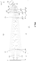
- FIG. 2 is a view illustrating a laser polycrystallization apparatus according to an exemplary embodiment of the present invention.
- the laser polycrystallization apparatus 1000 includes a light source 200, a diffraction grating 300, a light split portion 400, and a light superposition portion 500, as illustrated in FIG. 2 .
- the light source 200 is a laser light source, which emits a laser beam 110.
- the laser beam 110 emitted from the light source 200 has an energy density of a Gaussian distribution.
- a center energy density of the laser beam 110 is higher than an energy density of a peripheral portion of the laser beam 110.
- the diffraction grating 300 receives the laser beam 110 from the light source 200, changes a path of the incident laser beam 110, and emits the laser beam 110 with the changed path.
- the diffraction grating 300 expands a size of the laser beam 110 in one direction and emits it.
- the diffraction grating 300 expands the laser beam 110 in the major axis direction (e.g., an X-axis direction) or the minor axis direction (e.g., a Y-axis direction) to increase its magnification.
- the laser beam 111 of which magnification is increased is irradiated to the light split portion 400.
- the beam width in the major axis direction e.g., an X-axis direction
- the minor axis direction e.g., a Y-axis direction
- the light split portion 400 splits the laser beam 111 incident thereto from the diffraction grating 300 to generate a plurality of sub-laser beams 112a.
- the light split portion 400 generates a laser beam 112 including a plurality of sub-laser beams 112a.
- the light split portion 400 may include a first lens array 401 and a second lens array 402.
- the first lens array 401 is located between the diffraction grating 300 and the light superposition portion 500.
- the first lens array 401 is located between the diffraction grating 300 and the second lens array 402.
- the first lens array 401 may include a plurality of lenses 401a (hereinafter, "first lenses") to which the laser beam 111 is incident from the diffraction grating 300.
- Each first lens 401a may have a semi-cylindrical shape or a cylindrical shape.
- the plurality of first lenses 401a are located on an incidence surface of the first lens array 401. In other words, each of the first lenses 401a has a convex incidence surface.
- the plurality of first lenses 401a may be located on a surface of the first lens array 401 that faces the diffraction grating 300, and the convex surface of each first lens 401a may face the diffraction grating 300.
- the plurality of first lenses 401a are arranged along the major axis direction (e.g., the X-axis direction).
- each of the first lenses 401a may be a spherical lens or an aspherical lens.
- An emission surface of the first lens array 401 has a planar shape.
- each of the first lenses 401a has a flat emission surface from which the laser beam 112 is emitted from.
- the laser beam 111 incident to the first lens array 401 is refracted by each first lens 401a and divided into a plurality of sub-laser beams 112a.
- Each of the sub-laser beams 112a divided by the first lens array 401 is converged at a focus point f and then dispersed again to be incident to the second lens array 402.
- the second lens array 402 is located between the first lens array 401 and the light superposition portion 500.
- the second lens array 402 is located between the first lens array 401 and a first condensing lens 501.
- the second lens array 402 may include a plurality of lenses 402a (hereinafter, "second lenses") to which the laser beam 112 is incident from the first lens array 401.
- Each second lens 402a may have a semi-cylindrical shape or a cylindrical shape.
- the plurality of second lenses 402a are located on an incidence surface, facing the first lens array 401, of the second lens array 402. In other words, each of the second lenses 402a has a convex incidence surface.
- each second lens 402a may face the first lens array 401.
- the plurality of second lenses 402a are arranged along the major axis direction (e.g., the X-axis direction).
- the number of second lenses 402a included in the second lens array 402 may be substantially equal to the number of first lenses 401a included in the first lens array 401.
- each of the second lenses 402a may be a spherical lens or an aspherical lens.
- An emission surface of the second lens array 402 has a planar shape.
- each of the second lenses 402a has a flat emission surface.
- the laser beam 112 incident to the second lens array 402 is refracted by each second lens 402a and emitted to the light superposition portion 500.
- the light superposition portion 500 superposes the sub-laser beams 112a, which are incident thereto, split by the light split portion 400 and emits them.
- the light superposition portion 500 receives the laser beam 112 from the second lens array 402, superposes the plurality of sub-laser beams 112a included in the irradiated laser beam 112, and emits the superposed sub-laser beams 112a.
- the light superposition portion 500 may include at least one condensing lens.
- the light superposition portion 500 may include a first condensing lens 501 and a second condensing lens 502.
- the first condensing lens 501 is located between the light split portion 400 and the substrate 10.
- the first condensing lens 501 is located between the second lens array 402 and the second condensing lens 502.
- the second condensing lens 502 is located between the first condensing lens 501 and the substrate 10.
- the first condensing lens 501 has a flat incidence surface and a convex emission surface
- the second condensing lens 502 has a convex incidence surface and a flat emission surface.
- the convex surface of the first condensing lens 501 and the convex surface of the second condensing lens 502 face each other.
- the first condensing lens 501 refracts and diffuses the sub-laser beams 112a in the major axis direction (e.g., the X-axis direction), and emits them.
- the sub-laser beams 112a emitted from the first condensing lens 501 are received by the second condensing lens 502 in which the sub-laser beams 112a are refracted and emitted.
- the sub-laser beams 112a emitted from the second condensing lens 502 have a uniform energy density in the major axis direction (e.g., the X-axis direction).
- the sub-laser beams 112a having passed through the second condensing lens 502 are irradiated to the substrate 10.
- the laser beam 210 having passed through the second condensing lens 502 includes a plurality of sub-laser beams 112a, and such a laser beam 210 is irradiated to the substrate 10.
- the plurality of sub-laser beams 112a may be focused on points of the substrate 10.
- a distance d1 between the diffraction grating 300 and the first lens array 401 may be in a range from about 100 mm to about 1,000 mm.
- the distance d1 between the emission surface of the diffraction grating 300 and the incidence surface of the first lens array 401 may be in a range from about 100 mm to about 1,000 mm.
- a distance d2 between the first lens array 401 and the second lens array 402 may be about 135 mm.
- the distance d2 between the emission surface of the first lens array 401 and the incidence surface of the second lens array 402 may be about 135 mm.
- a distance d3 between the second lens array 402 and the first condensing lens 501 may be about 323 mm.
- the distance d3 between the emission surface of the second lens array 402 and the incidence surface of the first condensing lens 501 may be about 323 mm.
- a distance d4 between the first condensing lens 501 and the second condensing lens 502 may be about 14,000 mm.
- the distance d4 between the emission surface of the first condensing lens 501 and the incidence surface of the second condensing lens 502 may be about 14,000 mm.
- a distance d5 between the second condensing lens 502 and the substrate 10 may be about 500 mm.
- the distance d5 between the emission surface of the second condensing lens 502 and an irradiation surface of the substrate 10 may be about 500 mm.
- a thickness t1 of the first lens 401a included in the first lens array 401 may be about 3 mm, and a radius of curvature of the first lens 401a included in the first lens array 401 may be about 110.8 mm.
- a thickness t2 of the second lens 402a included in the second lens array 402 may be about 3 mm, and a radius of curvature of the second lens 402a included in the second lens array 402 may be about 25.7 mm.
- a thickness t3 of the first condensing lens 501 may be about 40 mm, and a radius of curvature of the first condensing lens 501 may be about 6,822 mm.
- a thickness t4 of the second condensing lens 502 may be about 50 mm, and a radius of curvature of the second condensing lens 502 may be about 6,822 mm.
- At least one of the diffraction grating 300, the first lens array 401, the second lens array 402, the first condensing lens 501, and the second condensing lens 502 may include a material including fused silica.
- an air layer may be positioned between the first lens array 401 and the second lens array 402, between the second lens array 402 and the first condensing lens 501, and between the first condensing lens 501 and the second condensing lens 502.
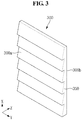
- FIG. 3 is a perspective view illustrating a diffraction grating of FIG. 2 according to an exemplary embodiment of the present invention
- FIG. 4 is a view enlarging a light source, a diffraction grating, a first lens array and a second lens array of FIG. 2 according to an exemplary embodiment of the present invention
- FIG. 5 is a view illustrating an intensity in a major axis direction of a laser beam emitted from a light superposition portion of FIG. 2 according to an exemplary embodiment of the present invention.
- An abscissa axis of FIG. 5 represents a cross-section of the laser beam
- an ordinate axis of FIG. 5 represents an intensity of the laser beam.
- the diffraction grating 300 includes a plurality of gratings 350 arranged along the major axis direction (e.g., the X-axis direction).
- Each grating 350 may have a triangular shape from a cross-sectional view.
- each grating 350 may be slanted at an angle with respect to an emission surface 300b of the diffraction grating 300.
- a bottom surface of each grating 350 extends in a direction away from the emission surface 300b of the diffraction grating 300.
- a bottom surface of each grating 350 included in the diffraction grating 300 faces downward (e.g., a negative X-direction).
- the diffraction grating 300 may include gratings 350 with a rectangular shape.
- the present invention is not limited thereto.
- an angle ⁇ (hereinafter, "an incidence angle") between the laser beam 110, which is irradiated from the light source 200 to an incidence surface 300a of the diffraction grating 300, and a normal line 311 of the emission surface 300b of the diffraction grating 300 is an acute angle.
- the incidence angle ⁇ may be in a range from about 5 degrees to about 65 degrees.
- the incidence angle may be about 45 degrees.
- the normal line 311 may be an imaginary line that extends perpendicular to the emission surface 300b of the diffraction grating 300.
- the laser beam 111 having passed through the diffraction grating 300 has a size larger than a size of the laser beam 110 before passing through the diffraction grating 300 due to the incidence angle ⁇ of the laser beam 110.
- a magnification of the laser beam 111 passing through the diffraction grating 300 increases.
- the laser beam 111 having passed through the diffraction grating 300 has a width W2 which is larger in the major axis direction (e.g., the X-axis direction) than a width W1 of the laser beam 110 emitted from the light source 200 (e.g., W2 > W1).
- the width W2 of the laser beam 111 having passed through the diffraction grating 300 is larger than the width W1 of the laser beam 110 before passing through the diffraction grating 300. Since the size of the laser beam 111 passing through the diffraction grating 300 increases in such a manner, the magnification of the laser beam 111 may increase without using a plurality of telescope lenses. Accordingly, the structure of the laser polycrystallization apparatus 1000 may be simplified.
- the diffraction grating 300 may have a diffraction angle of about 0 degrees.
- the diffraction angle is an angle formed by the normal line 311 of the diffraction grating 300 and the laser beam 111 emitted from the diffraction grating 300.
- the diffraction grating 300 may function with light having a wavelength of about 343 nm. In other words, the diffraction grating 300 may have a working wavelength of 343 nm.
- the laser beam 110 emitted from the light source 200 may include a plurality of sub-beams L1, L2, L3, L4, L5 and L6, as illustrated in FIG. 4 .
- the sub-beams L1, L2, L3, L4, L5 and L6 are parallel to each other.
- the sub-beams L1, L2, L3, L4, L5 and L6 are incident to the incidence surface 300a of the diffraction grating 300 at the aforementioned incidence angle ⁇ . Accordingly, each of the sub-beams L1, L2, L3, L4, L5 and L6 incident to the incidence surface 300a of the diffraction grating 300 has optical paths of different lengths.
- a sub-beam L1 of the sub-beams L1, L2, L3, L4, L5 and L6 which is incident to an uppermost portion of the incidence surface 300a of the diffraction grating 300 has a longest optical path
- a sub-beam L6 of the sub-beams L1, L2, L3, L4, L5 and L6 which is incident to a lowermost portion of the incidence surface 300a of the diffraction grating 300 has a shortest optical path.
- the closer a sub-beam is incident to an upper portion of the diffraction grating 300 the longer the optical path will be for that sub-beam.
- a phase delay occurs between the sub-beams L1, L2, L3, L4, L5 and L6, such that a coherence between the sub-beams L1, L2, L3, L4, L5 and L6 may be substantially minimized. Accordingly, a speckle noise of the laser beam 210 incident to the substrate 10 may be substantially minimized.
- the laser beam 110 emitted from the light source 200 has an energy density of a Gaussian distribution.
- an energy density of the sub-beams L3 and L4 located at a center portion of the laser beam 110 is relatively high, and an energy density of the sub-beams L1, L2, L5, and L6 located at a peripheral portion of the laser beam is relatively low.
- the diffraction grating 300 may be a blazed refraction grating or a blazed transmission grating which may achieve a maximum efficiency of the diffraction grating 300 at a specific diffraction order or a specific spectrum order. In the case where such a diffraction grating 300 is used, most of the optical power may achieve a maximum efficiency of the diffraction grating 300 at a specific diffraction order, and light output loss may be substantially minimized in other diffraction orders. For example, this loss may be nearly zero.
- Such a diffraction grating 300 may operate at a specific wavelength length, for example, a blaze wavelength.
- a lattice equation of the diffraction grating 300 may be denoted by the following equation (Equation 1).
- Equation 1 A lattice equation of the diffraction grating 300 may be denoted by the following equation (Equation 1).
- Equation 1 d represents a lattice constant, ⁇ represents an incidence angle, ⁇ represents a diffraction angle, m represents a diffraction order, and ⁇ represents a wavelength of an incident light (e.g., a light incident from the light source 200 to the incidence surface 300a of the diffraction grating 300).
- a geometry grating magnification M of the diffraction grating 300 illustrated in FIG. 4 may be calculated by the following equation (Equation 2).
- M 1 / cos ⁇
- a phase delay of the sub-beams L1, L2, L3, L4, L5 and L6 passing through adjacent first lenses 401a of the first lens array 401 may be determined by the following equation (Equation 3).
- ⁇ P LA / sin ⁇
- Equation 3 P LA represents a pitch of the first lens 401a (or the second lens 402a).
- the spatial coherence length L may be about 7.8 mm.
- the incidence angle ⁇ of the aforementioned diffraction grating 300 may be about 45 degrees and the diffraction angle ⁇ of the diffraction grating 300 may be about 0 degrees.
- the lattice constant d may be about 485 um.
- the phase delay between sub-beams having the pitch P LA of about 8 mm may be about 11.3 mm. This value is larger than the coherence length of about 7.8 mm. Accordingly, the distribution of the laser beam 210 irradiated to the substrate 10 might not be affected by interference effects.
- the laser beam 210 irradiated to the substrate 10 may have an intensity homogenized in the major axis direction (e.g., the X-axis direction), as illustrated in FIG. 5 .
- the magnification M in the Equation 2 may be about 1.4.
- FIG. 6 is a view enlarging the light source, the diffraction grating, the first lens array and the second lens array of FIG. 2 according to an exemplary embodiment of the present invention.
- a bottom surface of a grating 350 included in a diffraction grating 300 faces upward (e.g., the X-direction).
- the bottom surface of the grating 350 included in the diffraction grating 300 of FIG. 4 faces downward
- the bottom surface of the grating 350 included in the diffraction grating 300 of FIG. 6 faces upward.
- embodiments of the invention can provide a laser polycrystallization apparatus, comprising: a light source for emitting a laser beam; a diffraction grating for receiving the laser beam from the light source, changing a path and increasing a size (e.g. a beam width) of the received laser beam (e.g.
- a light split portion for splitting the changed laser beam received from the diffraction grating into split laser beams; and a light superposition portion for superposing the split laser beams received from the light split portion and irradiating the superposed split laser beams to a substrate, wherein an angle between the laser beam irradiated to an incidence surface of the diffraction grating from the light source and a line substantially perpendicular to an emission surface of the diffraction grating is an acute angle.
- the diffraction grating may be arranged to increase a size of the received laser beam in one direction.
- the diffraction grating may be arranged to increase a beam width of the received laser beam.
- Embodiments can enable a substantially uniform energy density in the major axis direction on the substrate.
- the light split portion comprises: a first lens array located between the diffraction grating and the light superposition portion and comprising a plurality of first lenses; and a second lens array located between the first lens array and the light superposition portion and comprising a plurality of second lenses.
- Embodiments of the invention can also provide a laser polycrystallization apparatus, comprising: a light source; a diffraction grating including a plurality of gratings, each grating having a triangular shape; a first lens array including a plurality of first lenses; a second lens array including a plurality of second lenses, wherein the first lens array is disposed between the second lens array and the diffraction grating; a first condensing lens including an emission surface with a convex shape; and a second condensing lens including an incidence surface with a convex shape, wherein the incidence surface of the second condensing lens faces the emission surface of the first condensing lens.
- the laser polycrystallization apparatus provides the following effects.
- a laser beam from a light source is incident on a diffraction grating at an acute angle. Accordingly, each sub-beam of the laser beam incident to the diffraction grating has an optical path of a different length. Due to the difference in the lengths of the optical paths, a phase delay is generated between the sub-beams, and accordingly, a coherence between the sub-beams may be substantially minimized. Therefore, the speckle noise of the laser beam incident to the substrate may be substantially minimized.
- a size of the laser beam passing through the diffraction grating increases. Accordingly, a magnification of the laser beam may be increased without a plurality of telescope lenses. Therefore, the configuration of the laser polycrystallization apparatus may be substantially simplified.
Landscapes
- Physics & Mathematics (AREA)
- Optics & Photonics (AREA)
- Engineering & Computer Science (AREA)
- Electromagnetism (AREA)
- Plasma & Fusion (AREA)
- General Physics & Mathematics (AREA)
- Mechanical Engineering (AREA)
- Condensed Matter Physics & Semiconductors (AREA)
- Manufacturing & Machinery (AREA)
- Recrystallisation Techniques (AREA)
- Laser Beam Processing (AREA)
- Chemical & Material Sciences (AREA)
- Crystallography & Structural Chemistry (AREA)
- Diffracting Gratings Or Hologram Optical Elements (AREA)
- Chemical Kinetics & Catalysis (AREA)
- Microelectronics & Electronic Packaging (AREA)
Applications Claiming Priority (1)
| Application Number | Priority Date | Filing Date | Title |
|---|---|---|---|
| KR1020160175628A KR102582652B1 (ko) | 2016-12-21 | 2016-12-21 | 레이저 결정화 장치 |
Publications (3)
| Publication Number | Publication Date |
|---|---|
| EP3340402A2 true EP3340402A2 (de) | 2018-06-27 |
| EP3340402A3 EP3340402A3 (de) | 2018-09-26 |
| EP3340402B1 EP3340402B1 (de) | 2022-01-26 |
Family
ID=60781753
Family Applications (1)
| Application Number | Title | Priority Date | Filing Date |
|---|---|---|---|
| EP17208649.8A Active EP3340402B1 (de) | 2016-12-21 | 2017-12-19 | Laser-polykristallisierungsvorrichtung |
Country Status (3)
| Country | Link |
|---|---|
| US (1) | US10403499B2 (de) |
| EP (1) | EP3340402B1 (de) |
| KR (1) | KR102582652B1 (de) |
Cited By (1)
| Publication number | Priority date | Publication date | Assignee | Title |
|---|---|---|---|---|
| US10991580B2 (en) | 2017-12-05 | 2021-04-27 | Samsung Display Co., Ltd. | Laser crystallizing apparatus |
Families Citing this family (5)
| Publication number | Priority date | Publication date | Assignee | Title |
|---|---|---|---|---|
| KR102582652B1 (ko) * | 2016-12-21 | 2023-09-25 | 삼성디스플레이 주식회사 | 레이저 결정화 장치 |
| IT201700114962A1 (it) * | 2017-10-12 | 2019-04-12 | Automotive Lighting Italia Spa | Attrezzatura di saldatura laser simultanea di un fanale automobilistico e metodo di saldatura laser simultanea di un fanale automobilistico |
| KR102688794B1 (ko) * | 2019-01-11 | 2024-07-29 | 삼성디스플레이 주식회사 | 레이저 결정화 장치 |
| EP3855219B1 (de) * | 2020-01-21 | 2024-09-18 | Focuslight Technologies Inc. | Diffusorvorrichtung |
| KR102798220B1 (ko) * | 2021-12-29 | 2025-04-23 | 주식회사 아큐레이저 | 빔의 조사 영역을 재배치하는 빔 재배치부를 포함하여 이루어진 레이저 조사 장치 |
Family Cites Families (28)
| Publication number | Priority date | Publication date | Assignee | Title |
|---|---|---|---|---|
| JP3301054B2 (ja) * | 1996-02-13 | 2002-07-15 | 株式会社半導体エネルギー研究所 | レーザー照射装置及びレーザー照射方法 |
| JPH09234579A (ja) * | 1996-02-28 | 1997-09-09 | Semiconductor Energy Lab Co Ltd | レーザー照射装置 |
| JP2001183605A (ja) * | 1999-02-04 | 2001-07-06 | Matsushita Electric Ind Co Ltd | 回折、散乱をなす光学素子を使用した投光、表示装置 |
| EP1661656B1 (de) * | 1999-04-02 | 2008-03-19 | Murata Manufacturing Co., Ltd. | Laserverfahren zur Bearbeitung von Löchern nur in einer keramischen Grünfolie mit einem Trägerfilm |
| EP1076359B1 (de) * | 1999-08-13 | 2011-02-23 | Semiconductor Energy Laboratory Co., Ltd. | Laserbestrahlungsgerät |
| JP3365500B2 (ja) | 2000-01-19 | 2003-01-14 | ウシオ電機株式会社 | 狭帯化ArFエキシマレーザ装置 |
| AU2001274079A1 (en) | 2000-05-30 | 2001-12-11 | Thomson Licensing S.A. | Device for reading and/or writing optical recording media |
| TW523791B (en) * | 2000-09-01 | 2003-03-11 | Semiconductor Energy Lab | Method of processing beam, laser irradiation apparatus, and method of manufacturing semiconductor device |
| TWI240151B (en) | 2000-10-10 | 2005-09-21 | Asml Netherlands Bv | Lithographic apparatus, device manufacturing method, and device manufactured thereby |
| US6665471B1 (en) * | 2001-08-13 | 2003-12-16 | Nlight Photonics Corporation | System and method for optimizing the performance of multiple gain element laser |
| JP4859311B2 (ja) * | 2001-09-17 | 2012-01-25 | 株式会社リコー | レーザ照明光学系、該光学系を用いた露光装置、レーザ加工機、及び投射装置 |
| US7170600B2 (en) * | 2002-09-20 | 2007-01-30 | Nippon Sheet Glass Company, Limited | Spectrometer using diffraction grating |
| DE10345177B3 (de) | 2003-09-29 | 2004-10-21 | Innovavent Gmbh | Linsensystem zum Homogenisieren von Laserpulsen |
| JP4579575B2 (ja) * | 2004-05-14 | 2010-11-10 | 株式会社半導体エネルギー研究所 | レーザ照射方法及びレーザ照射装置 |
| JP5072197B2 (ja) * | 2004-06-18 | 2012-11-14 | 株式会社半導体エネルギー研究所 | レーザ照射装置およびレーザ照射方法 |
| CN101331592B (zh) * | 2005-12-16 | 2010-06-16 | 株式会社半导体能源研究所 | 激光照射设备、激光照射方法和半导体装置的制造方法 |
| JP2007214527A (ja) * | 2006-01-13 | 2007-08-23 | Ihi Corp | レーザアニール方法およびレーザアニール装置 |
| JP2008052826A (ja) * | 2006-08-24 | 2008-03-06 | Funai Electric Co Ltd | 光ピックアップ装置 |
| US7662703B2 (en) * | 2006-08-31 | 2010-02-16 | Semiconductor Energy Laboratory Co., Ltd. | Method for manufacturing crystalline semiconductor film and semiconductor device |
| US7436588B2 (en) * | 2006-10-05 | 2008-10-14 | Northrop Grumman Corporation | Method and system for hybrid coherent and incoherent diffractive beam combining |
| TWI394152B (zh) * | 2007-07-30 | 2013-04-21 | Sony Corp | Objective lens, optical read / write head and optical disc device |
| EP2237079B1 (de) | 2009-04-03 | 2013-05-29 | Innovavent GmbH | Vorrichtung zum Homogenisieren kohärenter Strahlung |
| US8432613B2 (en) * | 2009-04-21 | 2013-04-30 | Applied Materials, Inc. | Multi-stage optical homogenization |
| US8902506B2 (en) | 2010-09-30 | 2014-12-02 | Panasonic Corporation | Laser speckle reduction element |
| KR101298019B1 (ko) * | 2010-12-28 | 2013-08-26 | (주)큐엠씨 | 레이저 가공 장치 |
| US9190807B2 (en) * | 2013-12-16 | 2015-11-17 | TeraDiode, Inc. | Method for improving performance of wavelength beam combining diode laser systems |
| CN105932545A (zh) * | 2016-07-06 | 2016-09-07 | 上海高意激光技术有限公司 | 一种激光阵列合束装置 |
| KR102582652B1 (ko) * | 2016-12-21 | 2023-09-25 | 삼성디스플레이 주식회사 | 레이저 결정화 장치 |
-
2016
- 2016-12-21 KR KR1020160175628A patent/KR102582652B1/ko active Active
-
2017
- 2017-12-19 EP EP17208649.8A patent/EP3340402B1/de active Active
- 2017-12-20 US US15/848,086 patent/US10403499B2/en active Active
Non-Patent Citations (1)
| Title |
|---|
| None |
Cited By (2)
| Publication number | Priority date | Publication date | Assignee | Title |
|---|---|---|---|---|
| US10991580B2 (en) | 2017-12-05 | 2021-04-27 | Samsung Display Co., Ltd. | Laser crystallizing apparatus |
| US11532476B2 (en) | 2017-12-05 | 2022-12-20 | Samsung Display Co., Ltd. | Laser crystallizing apparatus |
Also Published As
| Publication number | Publication date |
|---|---|
| EP3340402B1 (de) | 2022-01-26 |
| US10403499B2 (en) | 2019-09-03 |
| EP3340402A3 (de) | 2018-09-26 |
| KR20180072906A (ko) | 2018-07-02 |
| KR102582652B1 (ko) | 2023-09-25 |
| US20180174836A1 (en) | 2018-06-21 |
Similar Documents
| Publication | Publication Date | Title |
|---|---|---|
| EP3340402B1 (de) | Laser-polykristallisierungsvorrichtung | |
| US8569814B2 (en) | Laser annealing method and laser annealing device | |
| KR102589766B1 (ko) | 레이저 장치 | |
| US10957541B2 (en) | Short pulse fiber laser for LTPS crystallization | |
| JP5274085B2 (ja) | レーザー加工装置、レーザービームのピッチ可変方法、及びレーザー加工方法 | |
| US10654130B2 (en) | Polarization module and laser apparatus including the same | |
| JP5133158B2 (ja) | 多重ビームレーザー装置 | |
| TWI630638B (zh) | 執行雷射結晶之方法 | |
| KR102904602B1 (ko) | 레이저 처리 장치 및 레이저 광 모니터 방법 | |
| US7176042B2 (en) | Laser beam irradiation method that includes determining a thickness of semiconductor prior to crystallizing | |
| US7550694B2 (en) | Laser anneal apparatus | |
| JP5745746B2 (ja) | 光ビーム不均一性補正デバイス及び光ビームの強度分布を補正する方法 | |
| KR20090008942A (ko) | 다중 빔 레이저 장치 및 빔 스플리터 | |
| JP2008218741A (ja) | レーザーアニール装置及びレーザーアニール方法 | |
| KR102796148B1 (ko) | 실리콘 결정화 장치 | |
| JP4652707B2 (ja) | 結晶化装置、結晶化方法、位相変調素子、およびデバイス | |
| US20060177973A1 (en) | Generation method of light intensity distribution, generation apparatus of light intensity distribution, and light modulation element assembly | |
| JP2006054222A (ja) | 光変調素子、結晶化装置、結晶化方法、薄膜半導体基板の製造装置、薄膜半導体基板の製造方法、薄膜半導体装置、薄膜半導体装置の製造方法および表示装置 | |
| US20230201962A1 (en) | Laser machining device | |
| JP2011139082A (ja) | 光変調素子、結晶化装置、結晶化方法、薄膜半導体基板の製造装置、薄膜半導体基板の製造方法、薄膜半導体装置、薄膜半導体装置の製造方法および表示装置 | |
| JP2006024796A (ja) | 光照射装置、結晶化装置、結晶化方法、およびデバイス | |
| JP2009094329A (ja) | 結晶化装置、結晶化方法、およびデバイス |
Legal Events
| Date | Code | Title | Description |
|---|---|---|---|
| PUAI | Public reference made under article 153(3) epc to a published international application that has entered the european phase |
Free format text: ORIGINAL CODE: 0009012 |
|
| STAA | Information on the status of an ep patent application or granted ep patent |
Free format text: STATUS: THE APPLICATION HAS BEEN PUBLISHED |
|
| AK | Designated contracting states |
Kind code of ref document: A2 Designated state(s): AL AT BE BG CH CY CZ DE DK EE ES FI FR GB GR HR HU IE IS IT LI LT LU LV MC MK MT NL NO PL PT RO RS SE SI SK SM TR |
|
| AX | Request for extension of the european patent |
Extension state: BA ME |
|
| PUAL | Search report despatched |
Free format text: ORIGINAL CODE: 0009013 |
|
| AK | Designated contracting states |
Kind code of ref document: A3 Designated state(s): AL AT BE BG CH CY CZ DE DK EE ES FI FR GB GR HR HU IE IS IT LI LT LU LV MC MK MT NL NO PL PT RO RS SE SI SK SM TR |
|
| AX | Request for extension of the european patent |
Extension state: BA ME |
|
| RIC1 | Information provided on ipc code assigned before grant |
Ipc: H01J 29/46 20060101ALI20180817BHEP Ipc: H01S 5/00 20060101AFI20180817BHEP Ipc: B23K 26/067 20060101ALI20180817BHEP Ipc: H01J 9/24 20060101ALI20180817BHEP Ipc: H01S 5/40 20060101ALI20180817BHEP |
|
| STAA | Information on the status of an ep patent application or granted ep patent |
Free format text: STATUS: REQUEST FOR EXAMINATION WAS MADE |
|
| 17P | Request for examination filed |
Effective date: 20181221 |
|
| RBV | Designated contracting states (corrected) |
Designated state(s): AL AT BE BG CH CY CZ DE DK EE ES FI FR GB GR HR HU IE IS IT LI LT LU LV MC MK MT NL NO PL PT RO RS SE SI SK SM TR |
|
| STAA | Information on the status of an ep patent application or granted ep patent |
Free format text: STATUS: EXAMINATION IS IN PROGRESS |
|
| 17Q | First examination report despatched |
Effective date: 20190515 |
|
| REG | Reference to a national code |
Ref country code: DE Ref legal event code: R079 Ref document number: 602017052718 Country of ref document: DE Free format text: PREVIOUS MAIN CLASS: H01S0005000000 Ipc: H01J0029460000 |
|
| GRAP | Despatch of communication of intention to grant a patent |
Free format text: ORIGINAL CODE: EPIDOSNIGR1 |
|
| STAA | Information on the status of an ep patent application or granted ep patent |
Free format text: STATUS: GRANT OF PATENT IS INTENDED |
|
| RIC1 | Information provided on ipc code assigned before grant |
Ipc: H01J 29/46 20060101AFI20210630BHEP Ipc: B23K 26/067 20060101ALI20210630BHEP Ipc: H01J 9/24 20060101ALI20210630BHEP Ipc: H01S 3/00 20060101ALI20210630BHEP Ipc: H01L 21/02 20060101ALI20210630BHEP Ipc: B23K 26/06 20140101ALI20210630BHEP Ipc: B23K 103/00 20060101ALI20210630BHEP Ipc: H01L 27/12 20060101ALI20210630BHEP |
|
| INTG | Intention to grant announced |
Effective date: 20210728 |
|
| RIN1 | Information on inventor provided before grant (corrected) |
Inventor name: ASLANOV, EMIL Inventor name: RYU, JEKIL Inventor name: LEE, HAESOOK Inventor name: HAN, GYOOWAN |
|
| GRAS | Grant fee paid |
Free format text: ORIGINAL CODE: EPIDOSNIGR3 |
|
| GRAA | (expected) grant |
Free format text: ORIGINAL CODE: 0009210 |
|
| STAA | Information on the status of an ep patent application or granted ep patent |
Free format text: STATUS: THE PATENT HAS BEEN GRANTED |
|
| AK | Designated contracting states |
Kind code of ref document: B1 Designated state(s): AL AT BE BG CH CY CZ DE DK EE ES FI FR GB GR HR HU IE IS IT LI LT LU LV MC MK MT NL NO PL PT RO RS SE SI SK SM TR |
|
| REG | Reference to a national code |
Ref country code: GB Ref legal event code: FG4D |
|
| REG | Reference to a national code |
Ref country code: CH Ref legal event code: EP |
|
| REG | Reference to a national code |
Ref country code: AT Ref legal event code: REF Ref document number: 1465929 Country of ref document: AT Kind code of ref document: T Effective date: 20220215 |
|
| REG | Reference to a national code |
Ref country code: NL Ref legal event code: FP Ref country code: IE Ref legal event code: FG4D |
|
| REG | Reference to a national code |
Ref country code: DE Ref legal event code: R096 Ref document number: 602017052718 Country of ref document: DE |
|
| REG | Reference to a national code |
Ref country code: LT Ref legal event code: MG9D |
|
| REG | Reference to a national code |
Ref country code: AT Ref legal event code: MK05 Ref document number: 1465929 Country of ref document: AT Kind code of ref document: T Effective date: 20220126 |
|
| PG25 | Lapsed in a contracting state [announced via postgrant information from national office to epo] |
Ref country code: SE Free format text: LAPSE BECAUSE OF FAILURE TO SUBMIT A TRANSLATION OF THE DESCRIPTION OR TO PAY THE FEE WITHIN THE PRESCRIBED TIME-LIMIT Effective date: 20220126 Ref country code: RS Free format text: LAPSE BECAUSE OF FAILURE TO SUBMIT A TRANSLATION OF THE DESCRIPTION OR TO PAY THE FEE WITHIN THE PRESCRIBED TIME-LIMIT Effective date: 20220126 Ref country code: PT Free format text: LAPSE BECAUSE OF FAILURE TO SUBMIT A TRANSLATION OF THE DESCRIPTION OR TO PAY THE FEE WITHIN THE PRESCRIBED TIME-LIMIT Effective date: 20220526 Ref country code: NO Free format text: LAPSE BECAUSE OF FAILURE TO SUBMIT A TRANSLATION OF THE DESCRIPTION OR TO PAY THE FEE WITHIN THE PRESCRIBED TIME-LIMIT Effective date: 20220426 Ref country code: LT Free format text: LAPSE BECAUSE OF FAILURE TO SUBMIT A TRANSLATION OF THE DESCRIPTION OR TO PAY THE FEE WITHIN THE PRESCRIBED TIME-LIMIT Effective date: 20220126 Ref country code: HR Free format text: LAPSE BECAUSE OF FAILURE TO SUBMIT A TRANSLATION OF THE DESCRIPTION OR TO PAY THE FEE WITHIN THE PRESCRIBED TIME-LIMIT Effective date: 20220126 Ref country code: ES Free format text: LAPSE BECAUSE OF FAILURE TO SUBMIT A TRANSLATION OF THE DESCRIPTION OR TO PAY THE FEE WITHIN THE PRESCRIBED TIME-LIMIT Effective date: 20220126 Ref country code: BG Free format text: LAPSE BECAUSE OF FAILURE TO SUBMIT A TRANSLATION OF THE DESCRIPTION OR TO PAY THE FEE WITHIN THE PRESCRIBED TIME-LIMIT Effective date: 20220426 |
|
| PG25 | Lapsed in a contracting state [announced via postgrant information from national office to epo] |
Ref country code: PL Free format text: LAPSE BECAUSE OF FAILURE TO SUBMIT A TRANSLATION OF THE DESCRIPTION OR TO PAY THE FEE WITHIN THE PRESCRIBED TIME-LIMIT Effective date: 20220126 Ref country code: LV Free format text: LAPSE BECAUSE OF FAILURE TO SUBMIT A TRANSLATION OF THE DESCRIPTION OR TO PAY THE FEE WITHIN THE PRESCRIBED TIME-LIMIT Effective date: 20220126 Ref country code: GR Free format text: LAPSE BECAUSE OF FAILURE TO SUBMIT A TRANSLATION OF THE DESCRIPTION OR TO PAY THE FEE WITHIN THE PRESCRIBED TIME-LIMIT Effective date: 20220427 Ref country code: FI Free format text: LAPSE BECAUSE OF FAILURE TO SUBMIT A TRANSLATION OF THE DESCRIPTION OR TO PAY THE FEE WITHIN THE PRESCRIBED TIME-LIMIT Effective date: 20220126 Ref country code: AT Free format text: LAPSE BECAUSE OF FAILURE TO SUBMIT A TRANSLATION OF THE DESCRIPTION OR TO PAY THE FEE WITHIN THE PRESCRIBED TIME-LIMIT Effective date: 20220126 |
|
| PG25 | Lapsed in a contracting state [announced via postgrant information from national office to epo] |
Ref country code: IS Free format text: LAPSE BECAUSE OF FAILURE TO SUBMIT A TRANSLATION OF THE DESCRIPTION OR TO PAY THE FEE WITHIN THE PRESCRIBED TIME-LIMIT Effective date: 20220526 |
|
| REG | Reference to a national code |
Ref country code: DE Ref legal event code: R097 Ref document number: 602017052718 Country of ref document: DE |
|
| PG25 | Lapsed in a contracting state [announced via postgrant information from national office to epo] |
Ref country code: SM Free format text: LAPSE BECAUSE OF FAILURE TO SUBMIT A TRANSLATION OF THE DESCRIPTION OR TO PAY THE FEE WITHIN THE PRESCRIBED TIME-LIMIT Effective date: 20220126 Ref country code: SK Free format text: LAPSE BECAUSE OF FAILURE TO SUBMIT A TRANSLATION OF THE DESCRIPTION OR TO PAY THE FEE WITHIN THE PRESCRIBED TIME-LIMIT Effective date: 20220126 Ref country code: RO Free format text: LAPSE BECAUSE OF FAILURE TO SUBMIT A TRANSLATION OF THE DESCRIPTION OR TO PAY THE FEE WITHIN THE PRESCRIBED TIME-LIMIT Effective date: 20220126 Ref country code: EE Free format text: LAPSE BECAUSE OF FAILURE TO SUBMIT A TRANSLATION OF THE DESCRIPTION OR TO PAY THE FEE WITHIN THE PRESCRIBED TIME-LIMIT Effective date: 20220126 Ref country code: DK Free format text: LAPSE BECAUSE OF FAILURE TO SUBMIT A TRANSLATION OF THE DESCRIPTION OR TO PAY THE FEE WITHIN THE PRESCRIBED TIME-LIMIT Effective date: 20220126 Ref country code: CZ Free format text: LAPSE BECAUSE OF FAILURE TO SUBMIT A TRANSLATION OF THE DESCRIPTION OR TO PAY THE FEE WITHIN THE PRESCRIBED TIME-LIMIT Effective date: 20220126 |
|
| PG25 | Lapsed in a contracting state [announced via postgrant information from national office to epo] |
Ref country code: AL Free format text: LAPSE BECAUSE OF FAILURE TO SUBMIT A TRANSLATION OF THE DESCRIPTION OR TO PAY THE FEE WITHIN THE PRESCRIBED TIME-LIMIT Effective date: 20220126 |
|
| PLBE | No opposition filed within time limit |
Free format text: ORIGINAL CODE: 0009261 |
|
| STAA | Information on the status of an ep patent application or granted ep patent |
Free format text: STATUS: NO OPPOSITION FILED WITHIN TIME LIMIT |
|
| 26N | No opposition filed |
Effective date: 20221027 |
|
| PG25 | Lapsed in a contracting state [announced via postgrant information from national office to epo] |
Ref country code: SI Free format text: LAPSE BECAUSE OF FAILURE TO SUBMIT A TRANSLATION OF THE DESCRIPTION OR TO PAY THE FEE WITHIN THE PRESCRIBED TIME-LIMIT Effective date: 20220126 |
|
| P01 | Opt-out of the competence of the unified patent court (upc) registered |
Effective date: 20230516 |
|
| PG25 | Lapsed in a contracting state [announced via postgrant information from national office to epo] |
Ref country code: IT Free format text: LAPSE BECAUSE OF FAILURE TO SUBMIT A TRANSLATION OF THE DESCRIPTION OR TO PAY THE FEE WITHIN THE PRESCRIBED TIME-LIMIT Effective date: 20220126 |
|
| REG | Reference to a national code |
Ref country code: CH Ref legal event code: PL |
|
| REG | Reference to a national code |
Ref country code: BE Ref legal event code: MM Effective date: 20221231 |
|
| PG25 | Lapsed in a contracting state [announced via postgrant information from national office to epo] |
Ref country code: LU Free format text: LAPSE BECAUSE OF NON-PAYMENT OF DUE FEES Effective date: 20221219 |
|
| PG25 | Lapsed in a contracting state [announced via postgrant information from national office to epo] |
Ref country code: LI Free format text: LAPSE BECAUSE OF NON-PAYMENT OF DUE FEES Effective date: 20221231 Ref country code: IE Free format text: LAPSE BECAUSE OF NON-PAYMENT OF DUE FEES Effective date: 20221219 Ref country code: CH Free format text: LAPSE BECAUSE OF NON-PAYMENT OF DUE FEES Effective date: 20221231 |
|
| PG25 | Lapsed in a contracting state [announced via postgrant information from national office to epo] |
Ref country code: BE Free format text: LAPSE BECAUSE OF NON-PAYMENT OF DUE FEES Effective date: 20221231 |
|
| PG25 | Lapsed in a contracting state [announced via postgrant information from national office to epo] |
Ref country code: HU Free format text: LAPSE BECAUSE OF FAILURE TO SUBMIT A TRANSLATION OF THE DESCRIPTION OR TO PAY THE FEE WITHIN THE PRESCRIBED TIME-LIMIT; INVALID AB INITIO Effective date: 20171219 |
|
| PG25 | Lapsed in a contracting state [announced via postgrant information from national office to epo] |
Ref country code: CY Free format text: LAPSE BECAUSE OF FAILURE TO SUBMIT A TRANSLATION OF THE DESCRIPTION OR TO PAY THE FEE WITHIN THE PRESCRIBED TIME-LIMIT Effective date: 20220126 |
|
| PG25 | Lapsed in a contracting state [announced via postgrant information from national office to epo] |
Ref country code: MK Free format text: LAPSE BECAUSE OF FAILURE TO SUBMIT A TRANSLATION OF THE DESCRIPTION OR TO PAY THE FEE WITHIN THE PRESCRIBED TIME-LIMIT Effective date: 20220126 |
|
| PG25 | Lapsed in a contracting state [announced via postgrant information from national office to epo] |
Ref country code: MC Free format text: LAPSE BECAUSE OF FAILURE TO SUBMIT A TRANSLATION OF THE DESCRIPTION OR TO PAY THE FEE WITHIN THE PRESCRIBED TIME-LIMIT Effective date: 20220126 |
|
| PG25 | Lapsed in a contracting state [announced via postgrant information from national office to epo] |
Ref country code: MC Free format text: LAPSE BECAUSE OF FAILURE TO SUBMIT A TRANSLATION OF THE DESCRIPTION OR TO PAY THE FEE WITHIN THE PRESCRIBED TIME-LIMIT Effective date: 20220126 |
|
| PG25 | Lapsed in a contracting state [announced via postgrant information from national office to epo] |
Ref country code: MT Free format text: LAPSE BECAUSE OF FAILURE TO SUBMIT A TRANSLATION OF THE DESCRIPTION OR TO PAY THE FEE WITHIN THE PRESCRIBED TIME-LIMIT Effective date: 20220126 |
|
| PG25 | Lapsed in a contracting state [announced via postgrant information from national office to epo] |
Ref country code: TR Free format text: LAPSE BECAUSE OF FAILURE TO SUBMIT A TRANSLATION OF THE DESCRIPTION OR TO PAY THE FEE WITHIN THE PRESCRIBED TIME-LIMIT Effective date: 20220126 |
|
| PGFP | Annual fee paid to national office [announced via postgrant information from national office to epo] |
Ref country code: NL Payment date: 20251120 Year of fee payment: 9 |
|
| PGFP | Annual fee paid to national office [announced via postgrant information from national office to epo] |
Ref country code: DE Payment date: 20251120 Year of fee payment: 9 |
|
| PGFP | Annual fee paid to national office [announced via postgrant information from national office to epo] |
Ref country code: GB Payment date: 20251120 Year of fee payment: 9 |
|
| PGFP | Annual fee paid to national office [announced via postgrant information from national office to epo] |
Ref country code: FR Payment date: 20251125 Year of fee payment: 9 |