EP3304617B1 - Battery separator with dielectric coating - Google Patents
Battery separator with dielectric coating Download PDFInfo
- Publication number
- EP3304617B1 EP3304617B1 EP16804102.8A EP16804102A EP3304617B1 EP 3304617 B1 EP3304617 B1 EP 3304617B1 EP 16804102 A EP16804102 A EP 16804102A EP 3304617 B1 EP3304617 B1 EP 3304617B1
- Authority
- EP
- European Patent Office
- Prior art keywords
- separator
- porous
- dielectric layer
- dielectric
- implementations
- Prior art date
- Legal status (The legal status is an assumption and is not a legal conclusion. Google has not performed a legal analysis and makes no representation as to the accuracy of the status listed.)
- Active
Links
Images


Classifications
-
- H—ELECTRICITY
- H01—ELECTRIC ELEMENTS
- H01M—PROCESSES OR MEANS, e.g. BATTERIES, FOR THE DIRECT CONVERSION OF CHEMICAL ENERGY INTO ELECTRICAL ENERGY
- H01M4/00—Electrodes
- H01M4/02—Electrodes composed of, or comprising, active material
- H01M4/13—Electrodes for accumulators with non-aqueous electrolyte, e.g. for lithium-accumulators; Processes of manufacture thereof
-
- H—ELECTRICITY
- H01—ELECTRIC ELEMENTS
- H01M—PROCESSES OR MEANS, e.g. BATTERIES, FOR THE DIRECT CONVERSION OF CHEMICAL ENERGY INTO ELECTRICAL ENERGY
- H01M50/00—Constructional details or processes of manufacture of the non-active parts of electrochemical cells other than fuel cells, e.g. hybrid cells
- H01M50/40—Separators; Membranes; Diaphragms; Spacing elements inside cells
- H01M50/489—Separators, membranes, diaphragms or spacing elements inside the cells, characterised by their physical properties, e.g. swelling degree, hydrophilicity or shut down properties
-
- H—ELECTRICITY
- H01—ELECTRIC ELEMENTS
- H01M—PROCESSES OR MEANS, e.g. BATTERIES, FOR THE DIRECT CONVERSION OF CHEMICAL ENERGY INTO ELECTRICAL ENERGY
- H01M4/00—Electrodes
- H01M4/02—Electrodes composed of, or comprising, active material
- H01M4/64—Carriers or collectors
- H01M4/66—Selection of materials
- H01M4/661—Metal or alloys, e.g. alloy coatings
-
- H—ELECTRICITY
- H01—ELECTRIC ELEMENTS
- H01G—CAPACITORS; CAPACITORS, RECTIFIERS, DETECTORS, SWITCHING DEVICES, LIGHT-SENSITIVE OR TEMPERATURE-SENSITIVE DEVICES OF THE ELECTROLYTIC TYPE
- H01G11/00—Hybrid capacitors, i.e. capacitors having different positive and negative electrodes; Electric double-layer [EDL] capacitors; Processes for the manufacture thereof or of parts thereof
- H01G11/52—Separators
-
- H—ELECTRICITY
- H01—ELECTRIC ELEMENTS
- H01G—CAPACITORS; CAPACITORS, RECTIFIERS, DETECTORS, SWITCHING DEVICES, LIGHT-SENSITIVE OR TEMPERATURE-SENSITIVE DEVICES OF THE ELECTROLYTIC TYPE
- H01G9/00—Electrolytic capacitors, rectifiers, detectors, switching devices, light-sensitive or temperature-sensitive devices; Processes of their manufacture
- H01G9/004—Details
- H01G9/02—Diaphragms; Separators
-
- H—ELECTRICITY
- H01—ELECTRIC ELEMENTS
- H01M—PROCESSES OR MEANS, e.g. BATTERIES, FOR THE DIRECT CONVERSION OF CHEMICAL ENERGY INTO ELECTRICAL ENERGY
- H01M10/00—Secondary cells; Manufacture thereof
- H01M10/05—Accumulators with non-aqueous electrolyte
- H01M10/052—Li-accumulators
-
- H—ELECTRICITY
- H01—ELECTRIC ELEMENTS
- H01M—PROCESSES OR MEANS, e.g. BATTERIES, FOR THE DIRECT CONVERSION OF CHEMICAL ENERGY INTO ELECTRICAL ENERGY
- H01M4/00—Electrodes
- H01M4/02—Electrodes composed of, or comprising, active material
- H01M4/13—Electrodes for accumulators with non-aqueous electrolyte, e.g. for lithium-accumulators; Processes of manufacture thereof
- H01M4/134—Electrodes based on metals, Si or alloys
-
- H—ELECTRICITY
- H01—ELECTRIC ELEMENTS
- H01M—PROCESSES OR MEANS, e.g. BATTERIES, FOR THE DIRECT CONVERSION OF CHEMICAL ENERGY INTO ELECTRICAL ENERGY
- H01M4/00—Electrodes
- H01M4/02—Electrodes composed of, or comprising, active material
- H01M4/64—Carriers or collectors
- H01M4/66—Selection of materials
- H01M4/665—Composites
- H01M4/667—Composites in the form of layers, e.g. coatings
-
- H—ELECTRICITY
- H01—ELECTRIC ELEMENTS
- H01M—PROCESSES OR MEANS, e.g. BATTERIES, FOR THE DIRECT CONVERSION OF CHEMICAL ENERGY INTO ELECTRICAL ENERGY
- H01M50/00—Constructional details or processes of manufacture of the non-active parts of electrochemical cells other than fuel cells, e.g. hybrid cells
- H01M50/40—Separators; Membranes; Diaphragms; Spacing elements inside cells
- H01M50/403—Manufacturing processes of separators, membranes or diaphragms
- H01M50/406—Moulding; Embossing; Cutting
-
- H—ELECTRICITY
- H01—ELECTRIC ELEMENTS
- H01M—PROCESSES OR MEANS, e.g. BATTERIES, FOR THE DIRECT CONVERSION OF CHEMICAL ENERGY INTO ELECTRICAL ENERGY
- H01M50/00—Constructional details or processes of manufacture of the non-active parts of electrochemical cells other than fuel cells, e.g. hybrid cells
- H01M50/40—Separators; Membranes; Diaphragms; Spacing elements inside cells
- H01M50/409—Separators, membranes or diaphragms characterised by the material
- H01M50/411—Organic material
- H01M50/414—Synthetic resins, e.g. thermoplastics or thermosetting resins
- H01M50/417—Polyolefins
-
- H—ELECTRICITY
- H01—ELECTRIC ELEMENTS
- H01M—PROCESSES OR MEANS, e.g. BATTERIES, FOR THE DIRECT CONVERSION OF CHEMICAL ENERGY INTO ELECTRICAL ENERGY
- H01M50/00—Constructional details or processes of manufacture of the non-active parts of electrochemical cells other than fuel cells, e.g. hybrid cells
- H01M50/40—Separators; Membranes; Diaphragms; Spacing elements inside cells
- H01M50/409—Separators, membranes or diaphragms characterised by the material
- H01M50/431—Inorganic material
- H01M50/434—Ceramics
- H01M50/437—Glass
-
- H—ELECTRICITY
- H01—ELECTRIC ELEMENTS
- H01M—PROCESSES OR MEANS, e.g. BATTERIES, FOR THE DIRECT CONVERSION OF CHEMICAL ENERGY INTO ELECTRICAL ENERGY
- H01M50/00—Constructional details or processes of manufacture of the non-active parts of electrochemical cells other than fuel cells, e.g. hybrid cells
- H01M50/40—Separators; Membranes; Diaphragms; Spacing elements inside cells
- H01M50/409—Separators, membranes or diaphragms characterised by the material
- H01M50/446—Composite material consisting of a mixture of organic and inorganic materials
-
- H—ELECTRICITY
- H01—ELECTRIC ELEMENTS
- H01M—PROCESSES OR MEANS, e.g. BATTERIES, FOR THE DIRECT CONVERSION OF CHEMICAL ENERGY INTO ELECTRICAL ENERGY
- H01M50/00—Constructional details or processes of manufacture of the non-active parts of electrochemical cells other than fuel cells, e.g. hybrid cells
- H01M50/40—Separators; Membranes; Diaphragms; Spacing elements inside cells
- H01M50/409—Separators, membranes or diaphragms characterised by the material
- H01M50/449—Separators, membranes or diaphragms characterised by the material having a layered structure
- H01M50/451—Separators, membranes or diaphragms characterised by the material having a layered structure comprising layers of only organic material and layers containing inorganic material
-
- H—ELECTRICITY
- H01—ELECTRIC ELEMENTS
- H01M—PROCESSES OR MEANS, e.g. BATTERIES, FOR THE DIRECT CONVERSION OF CHEMICAL ENERGY INTO ELECTRICAL ENERGY
- H01M50/00—Constructional details or processes of manufacture of the non-active parts of electrochemical cells other than fuel cells, e.g. hybrid cells
- H01M50/40—Separators; Membranes; Diaphragms; Spacing elements inside cells
- H01M50/489—Separators, membranes, diaphragms or spacing elements inside the cells, characterised by their physical properties, e.g. swelling degree, hydrophilicity or shut down properties
- H01M50/491—Porosity
-
- H—ELECTRICITY
- H01—ELECTRIC ELEMENTS
- H01M—PROCESSES OR MEANS, e.g. BATTERIES, FOR THE DIRECT CONVERSION OF CHEMICAL ENERGY INTO ELECTRICAL ENERGY
- H01M50/00—Constructional details or processes of manufacture of the non-active parts of electrochemical cells other than fuel cells, e.g. hybrid cells
- H01M50/40—Separators; Membranes; Diaphragms; Spacing elements inside cells
- H01M50/489—Separators, membranes, diaphragms or spacing elements inside the cells, characterised by their physical properties, e.g. swelling degree, hydrophilicity or shut down properties
- H01M50/497—Ionic conductivity
-
- H—ELECTRICITY
- H01—ELECTRIC ELEMENTS
- H01M—PROCESSES OR MEANS, e.g. BATTERIES, FOR THE DIRECT CONVERSION OF CHEMICAL ENERGY INTO ELECTRICAL ENERGY
- H01M4/00—Electrodes
- H01M4/02—Electrodes composed of, or comprising, active material
- H01M2004/026—Electrodes composed of, or comprising, active material characterised by the polarity
- H01M2004/027—Negative electrodes
-
- Y—GENERAL TAGGING OF NEW TECHNOLOGICAL DEVELOPMENTS; GENERAL TAGGING OF CROSS-SECTIONAL TECHNOLOGIES SPANNING OVER SEVERAL SECTIONS OF THE IPC; TECHNICAL SUBJECTS COVERED BY FORMER USPC CROSS-REFERENCE ART COLLECTIONS [XRACs] AND DIGESTS
- Y02—TECHNOLOGIES OR APPLICATIONS FOR MITIGATION OR ADAPTATION AGAINST CLIMATE CHANGE
- Y02E—REDUCTION OF GREENHOUSE GAS [GHG] EMISSIONS, RELATED TO ENERGY GENERATION, TRANSMISSION OR DISTRIBUTION
- Y02E60/00—Enabling technologies; Technologies with a potential or indirect contribution to GHG emissions mitigation
- Y02E60/10—Energy storage using batteries
Definitions
- Implementations of the present disclosure generally relate to separators, high performance electrochemical devices, such as, batteries and capacitors, including the aforementioned separators, and methods for fabricating the same.
- Li-ion batteries typically include an anode electrode, a cathode electrode, and a separator positioned between the anode electrode and the cathode electrode.
- the separator is an electronic insulator, which provides physical and electrical separation between the cathode and the anode electrodes.
- the separator is typically made from micro-porous polyethylene and polyolefin.
- electrochemical reactions i.e., charging and discharging
- Li-ions are transported through the pores in the separator between the two electrodes via an electrolyte.
- electrochemical reactions i.e., charging and discharging
- Li-ions are transported through the pores in the separator between the two electrodes via an electrolyte.
- high porosity separators are susceptible to electrical shorts when lithium dendrites formed during cycling create shorts between the electrodes.
- separators which are then laminated together with anode and cathode electrodes in separate processing steps.
- Other separators are typically made by wet or dry extrusion of a polymer and then stretched to produce holes (tears) in the polymer.
- the separator is also one of the most expensive components in the Li-ion battery and accounts for over 20% of the material cost in battery cells.
- US patent application US 2004/106037 refers to a battery separator having an inorganic protective film and to a lithium battery using the separator.
- US patent application US 2013/337312 describes a separator for electrochemical devices, and a method for manufacturing the separator.
- European patent application EP 1 146 576 refers to a separator for high energy rechargeable lithium batteries.
- US patent application US 2014/133068 describes a capacitor including a capacitor element with a surface layer having pores and US patent application US 2013/199030 refers to a method of preparing lithium secondary battery.
- the present invention relates to separators and batteries comprising said separators as defined in the appended claims.
- Implementations of the present disclosure generally relate to separators, high performance electrochemical devices, such as, batteries and capacitors, including the aforementioned separators, and methods for fabricating the same.
- a separator for a battery is provided.
- the separator comprises a substrate capable of conducting ions and at least one dielectric layer capable of conducting ions.
- the at least one dielectric layer at least partially covers the substrate and has a thickness of 1 nanometer to 2,000 nanometers.
- a battery in another implementation, comprises an anode containing at least one of lithium metal or lithium-alloy or a mixture of lithium metal and/or lithium alloy and another material, tin, or silicon, a cathode, and a separator disposed between the anode and the cathode.
- the separator comprises a porous substrate capable of conducting ions and at least one dielectric layer capable of conducting ions.
- the at least one dielectric layer at least partially covers the substrate and has a thickness of 1 nanometer to 2,000 nanometers.
- a separator for a battery comprises at least one porous dielectric layer having a thickness of 1 nanometer to 2,000 nanometers and a microporous ion-conducting polymeric substrate adhered to the at least one porous dielectric layer.
- the porous dielectric layer is a porous aluminum oxide layer.
- the porous dielectric layer is a binder-free dielectric layer.
- the porous dielectric layer has a thickness in the range of 10 nanometers to 600 nanometers.
- the porous dielectric layer has a thickness in the range of 50 nanometers to 200 nanometers.
- the microporous ion-conducting polymeric substrate has a thickness in the range of 5 microns to 50 microns. In one implementation, the microporous ion-conducting polymeric substrate has a thickness in the range of 6 microns to 25 microns. In one implementation, the microporous ion-conducting polymeric substrate is a polyolefinic membrane. In one implementation, the polyolefinic membrane is a polyethylene membrane. In one implementation, the aluminum oxide layer further consists of: zirconium oxide, silicon oxide, or combinations thereof.
- a battery in yet another implementation, comprises an anode containing at least one of lithium metal or lithium-alloy or a mixture of lithium metal and/or lithium alloy and another material, tin, or silicon, a cathode, and a separator.
- the separator comprises at least one porous dielectric layer having a thickness of 1 nanometer to 2,000 nanometers and a microporous ion-conducting polymeric substrate adhered to the at least one porous dielectric layer.
- the battery further comprises an electrolyte in ionic communication with the anode and the cathode via the separator.
- the battery further comprises a positive current collector contacting the cathode and a negative current collector contacting the anode, wherein the positive current collector and the negative current collector are each independently comprises of materials selected from aluminum (Al), copper (Cu), zinc (Zn), nickel (Ni), cobalt (Co), tin (Sn), silicon (Si), manganese (Mn), magnesium (Mg), alloys thereof, and combinations thereof.
- a method of forming a separator for a rechargeable lithium-ion battery comprises exposing a material to be deposited on a porous ion-conducting polymer substrate positioned in a processing region to an evaporation process, flowing a reactive gas into the processing region and reacting the reactive gas and the evaporated material to deposit a dielectric layer on at least a portion of the porous ion-conducting polymer substrate.
- the material is selected from the group consisting of: aluminum (Al), zirconium (Zr), hafnium (Hf), niobium (Nb), tantalum (Ta), titanium (Ti), yttrium (Y), lanthanum (La), silicon (Si), boron (B), silver (Ag), chromium (Cr), copper (Cu), indium (In), iron (Fe), magnesium (Mg), calcium (Ca), strontium (Sr), barium (Ba), nickel (Ni), tin (Sn), ytterbium (Yb), lithium (Li) calcium or combinations thereof.
- the reactive gas is an oxygen-containing gas selected from the group consisting of: oxygen (O 2 ), ozone (O 3 ), oxygen radicals (O*), ionized oxygen atoms, carbon dioxide (CO 2 ), nitric oxide (NO x ), water vapor, or combinations thereof.
- the dielectric layer is aluminum oxide.
- the evaporation process is a thermal evaporation process or an electron beam evaporation process.
- the microporous ion-conducting polymeric substrate is exposed to a surface modification treatment process to enhance the nucleation/growth conditions of the microporous ion-conducting polymeric substrate.
- the surface modification treatment process comprises supplying a treatment gas mixture into the processing region and forming a plasma from the treatment gas mixture to plasma treat at least a portion of the microporous ion-conducting polymeric substrate, wherein the treatment gas mixture comprises an oxygen-containing gas, an inert gas, or combinations thereof.
- the method further comprises exposing the microporous ion-conducting polymeric substrate to a cooling process prior to exposing the material to an evaporation process.
- the cooling process cools the microporous ion-conducting polymeric substrate to a temperature between -20 degrees Celsius and 22 degrees Celsius.
- the cooling process cools the microporous ion-conducting polymeric substrate to a temperature between -10 degrees Celsius and 0 degrees Celsius.
- the evaporation process comprises exposing the material to a temperature of between 1,300 degrees Celsius and 1,600 degrees Celsius.
- the dielectric layer is a porous aluminum oxide layer.
- the dielectric layer is a binder-free dielectric layer.
- the dielectric layer has a thickness in the range of 1 nanometer and 2,000 nanometers. In one implementation, the dielectric layer has a thickness in the range of 10 nanometers to 500 nanometers.
- the microporous ion-conducting polymeric substrate has a thickness in the range of 5 microns to 50 microns. In one implementation, the microporous ion-conducting polymeric substrate has a thickness in the range of 6 microns to 25 microns. In one implementation, the microporous ion-conducting polymeric substrate is a polyolefinic membrane.
- the following disclosure describes separators, high performance electrochemical cells and batteries including the aforementioned separators, and methods for fabricating the same. Certain details are set forth in the following description and in FIGS. 1-9 to provide a thorough understanding of various implementations of the disclosure. Other details describing well-known structures and systems often associated with electrochemical cells and batteries are not set forth in the following disclosure to avoid unnecessarily obscuring the description of the various implementations.
- a pore size of about 10 nm generally indicates in its broadest sense 10 nm ⁇ 10%, which indicates 9.0-11.0 nm.
- the term “about” can indicate either a measurement error (i.e., by limitations in the measurement method), or alternatively, a variation or average in a physical characteristic of a group (e.g., a population of pores).
- crucible as used herein shall be understood as a unit capable of evaporating material that is fed to the crucible when the crucible is heated.
- a crucible is defined as a unit adapted for transforming solid material into vapor.
- the term “crucible” and “evaporation unit” are used synonymously.
- the texture of the material and the porosity data on the materials described herein can be analyzed by dinitrogen adsorption and desorption measurements.
- the specific surface area can be calculated by Brunauer-Emmett-Teller (BET) equation.
- BET Brunauer-Emmett-Teller
- the pore diameter distribution and the mean pore diameter can be calculated using Barrett-Joyner-Halenda (BJH) method from the adsorption branch of the N 2 adsorption-desorption isotherm.
- the currently available generation batteries especially Li-ion batteries, use porous polyolefin separators, which are susceptible to thermal shrinkage at elevated temperatures and may cause short between positive and negative electrodes or the corresponding current collectors.
- a ceramic coating on the separator helps to inhibit direct contact between electrodes and also helps to prevent potential dendrite growth associated with Li metal.
- Current state of the art ceramic coating is done using wet coating (e.g., slot-die techniques) of ceramic particles dispersed in a polymeric binder to make the composite and a solvent to make the slurry.
- the coating thickness is typically around 3 microns including randomly oriented dielectric material bound together by a polymer leading to a random pore structure.
- the existing ceramic particle coating method has difficulty in reducing tortuosity due to this random orientation of ceramic particles. Further, it is difficult to reduce the thickness of current ceramic coatings using current wet coating methods. In order to compensate for the increased surface area of finer ceramic powder particles current wet coating methods require increased amounts of both binder and solvent to decrease the viscosity of the slurry. Thus, the current wet coating methods suffer from several problems.
- a thin, low ionic resistance ceramic coating is formed on a polymeric microporous substrate, where the ceramic coating is formed by a dry method using reactive evaporation of metals or metal compounds. Further, the ceramic coating can be tuned for desired thickness, micro/nanostructure, multilayered structure, morphology, pore structure and pore/ceramic orientation.
- the reactive evaporation techniques described herein have at least one of the following advantages: (1) thinner separators result in less inactive component volume fraction and a corresponding increase in energy density and less ionic resistance across the separator; (2) the control of coating thickness and morphology provides less tortuous pores leading to superior separator performance; (3) the pore surface of the ceramic enhances the ionic conductivity of the overall electrolyte; and (4) suitably engineered ceramic coated separator shall enhance X-ray detection to determine manufacturing defects; and (5) higher voltage stability and puncture resistance properties of the separator can be achieved by nanocomposite coating control. Lithium dendrite inhibiting properties of ceramic-coated separator are enhanced by nanosurface engineering to achieve homogeneous lithium metal deposition and stripping during cycling.
- FIG. 1 illustrates an example Li-ion battery structure having a coated separator according to implementations of the present disclosure.
- Cell 100 has a positive current collector 110, a positive electrode 120, a coated separator 130, a negative electrode 140 and a negative current collector 150. Note in FIG. 1 that the current collectors are shown to extend beyond the stack, although it is not necessary for the current collectors to extend beyond the stack, the portions extending beyond the stack may be used as tabs.
- the current collectors 110, 150, on positive electrode 120 and negative electrode 140, respectively, can be identical or different electronic conductors.
- metals that the current collectors 110, 150 may be comprised of include aluminum (Al), copper (Cu), zinc (Zn), nickel (Ni), cobalt (Co), tin (Sn), silicon (Si), manganese (Mn), magnesium (Mg), alloys thereof, and combinations thereof.
- at least one of the current collectors 110, 150 is perforated.
- current collectors may be of any form factor (e.g., metallic foil, sheet, or plate), shape and micro/macro structure.
- tabs are formed of the same material as the current collector and may be formed during fabrication of the stack, or added later. All components except current collectors 110 and 150 contain lithium ion electrolytes.
- the negative electrode 140 or anode may be any material compatible with the positive electrode 120.
- the negative electrode 140 may have an energy capacity greater than or equal to 372 mAh/g, preferably ⁇ 700 mAh/g, and most preferably ⁇ 1000 mAh/g.
- the negative electrode 140 may be constructed from a lithium metal foil or a lithium alloy foil (e.g. lithium aluminum alloys), or a mixture of a lithium metal and/or lithium alloy and materials such as carbon (e.g. coke, graphite), nickel, copper, tin, indium, silicon, oxides thereof, or combinations thereof.
- the negative electrode 140 comprises intercalation compounds containing lithium or insertion compounds containing lithium.
- the positive electrode 120 or cathode may be any material compatible with the anode and may include an intercalation compound, an insertion compound, or an electrochemically active polymer.
- Suitable intercalation materials include, for example, lithium-containing metal oxides, MoS 2 , FeS 2 , MnO 2 , TiS 2 , NbSe 3 , LiCoO 2 , LiNiO 2 , LiMnO 2 , LiMn 2 O 4 , V 6 O 13 and V 2 O 5 .
- Suitable polymers include, for example, polyacetylene, polypyrrole, polyaniline, and polythiopene.
- the positive electrode 120 or cathode may be made from a layered oxide, such as lithium cobalt oxide, an olivine, such as lithium iron phosphate, or a spinel, such as lithium manganese oxide.
- exemplary lithium-containing oxides may be layered, such as lithium cobalt oxide (LiCoO 2 ), or mixed metal oxides, such as LiNi x Co 1-2x MnO 2 , LiNiMnCoO 2 ("NMC"), LiNi 0.5 Mn 1.5 O 4 , Li(Ni 0.8 CO 0.15 Al 0.05 )O 2 , LiMn 2 O 4 , and doped lithium rich layered-layered materials, wherein x is zero or a non-zero number.
- Exemplary phosphates may be iron olivine (LiFePO 4 ) and it is variants (such as LiFe (1-x) Mg x PO 4 ), LiMoPO 4 , LiCoPO 4 , LiNiPO 4 , Li 3 V 2 (PO 4 ) 3 , LiVOPO 4 , LiMP 2 O 7 , or LiFe 1.5 P 2 O 7 , wherein x is zero or a non-zero number.
- Exemplary fluorophosphates may be LiVPO 4 F, LiAlPO 4 F, Li 5 V(PO 4 ) 2 F 2 , Li 5 Cr(PO 4 ) 2 F 2 , Li 2 CoPO 4 F, or Li 2 NiPO 4 F.
- Exemplary silicates may be Li 2 FeSiO 4 , Li 2 MnSiO 4 , or Li 2 VOSiO 4 .
- An exemplary non-lithium compound is Na 5 V 2 (PO 4 ) 2 F 3 .
- lithium is contained in atomic layers of crystal structures of carbon graphite (LiC 6 ) at the negative electrode and lithium manganese oxide (LiMnO 4 ) or lithium cobalt oxide (LiCoO 2 ) at the positive electrode, for example, although in some implementations the negative electrode may also include lithium absorbing materials such as silicon, tin, etc.
- the cell even though shown as a planar structure, may also be formed into a cylinder by rolling the stack of layers; furthermore, other cell configurations (e.g., prismatic cells, button cells) may be formed.
- Electrolytes infused in cell components 120, 130 and 140 can be comprised of a liquid/gel or a solid polymer and may be different in each.
- the electrolyte primarily includes a salt and a medium (e.g., in a liquid electrolyte, the medium may be referred to as a solvent; in a gel electrolyte, the medium may be a polymer matrix).
- the salt may be a lithium salt.
- the lithium salt may include, for example, LiPF 6 , LiAsF 6 , LiCF 3 SO 3 , LiN(CF 3 SO 3 ) 3 , LiBF 6 , and LiClO 4 , BETTE electrolyte (commercially available from 3M Corp. of Minneapolis, MN) and combinations thereof.
- Solvents may include, for example, ethylene carbonate (EC), propylene carbonate (PC), EC/PC, 2-MeTHF(2-methyltetrahydrofuran)/EC/PC, EC/DMC (dimethyl carbonate), EC/DME (dimethyl ethane), EC/DEC (diethyl carbonate), EC/EMC (ethyl methyl carbonate), EC/EMC/DMC/DEC, EC/EMC/DMC/DEC/PE, PC/DME, and DME/PC.
- Polymer matrices may include, for example, PVDF (polyvinylidene fluoride), PVDF:THF (PVDF:tetrahydrofuran), PVDF:CTFE (PVDF: chlorotrifluoroethylene) PAN (polyacrylonitrile), and PEO (polyethylene oxide).
- PVDF polyvinylidene fluoride
- PVDF:THF PVDF:tetrahydrofuran
- PVDF:CTFE PVDF: chlorotrifluoroethylene
- PAN polyacrylonitrile
- PEO polyethylene oxide
- FIG. 2 illustrates a cross-sectional view of a coated separator 130 for a lithium-ion battery according to implementations described herein.
- the coated separator 130 comprises: a porous (e.g., microporous) polymeric substrate capable of conducting ions (e.g., a separator film) 131 with pores 132 and a first dielectric layer 133a and an optional second dielectric layer 133b (collectively dielectric layer 133) positioned on opposite surfaces of the porous polymeric substrate 131.
- the porous polymeric substrate itself does not need to be ion conducting, however, once filled with electrolyte (liquid, gel, solid, combination etc.), the combination of porous substrate and electrolyte is ion conducting.
- the dielectric layer 133 is, at least, adapted for preventing electronic shorting (e.g. direct or physical contact of the anode and the cathode) and blocking dendrite growth.
- the porous polymeric substrate 131 may be, at least, adapted for blocking (or shutting down) ionic conductivity (or flow) between the anode and the cathode during the event of thermal runaway.
- the dielectric layer 133 of the coated separator 130 should be sufficiently conductive to allow ionic flow between the anode and cathode, so that current, in desired quantities, may be generated by the cell.
- the porous polymeric substrate 131 and the dielectric layer 133 should adhere well to one another, i.e. separation should not occur.
- the dielectric layer 133 is formed on the porous polymeric substrate 131 using evaporation techniques.
- the porous polymeric substrate is a microporous ion-conducting polymeric substrate. In one implementation, the porous polymeric substrate is a multi-layer polymeric substrate. In one implementation, the pores 132 are micropores. In some implementations, the porous polymeric substrate 131 consists of any commercially available polymeric microporous membranes (e.g., single or multi-ply), for example, those products produced by produced by Polypore (Celgard Inc., of Charlotte, North Carolina), Toray Tonen (Battery separator film (BSF)), SK Energy (lithium ion battery separator (LiBS), Evonik industries (SEPARION® ceramic separator membrane), Asahi Kasei (HiporeTM polyolefin flat film membrane), DuPont (Energain®), etc.
- Polypore Cellular ion battery separator
- BSF Battery separator film
- SK Energy lithium ion battery separator
- Evonik industries SEPARION® ceramic separator membrane
- the porous polymeric substrate 131 has a porosity in the range of 20 to 80% (e.g., in the range of 28 to 60%). In some implementations, the porous polymeric substrate 131 has an average pore size in the range of 0.02 to 5 microns (e.g., 0.08 to 2 microns). In some implementations, the porous polymeric substrate 131 has a Gurley Number in the range of 15 to 150 seconds (Gurley Number refers to the time it takes for 10 cc of air at 12.2 inches of water to pass through one square inch of membrane). In some implementations, the porous polymeric substrate 131 is polyolefinic. Exemplary polyolefins include polypropylene, polyethylene, or combinations thereof.
- the dielectric layer 133 comprises one or more dielectric materials.
- the dielectric material may be a ceramic material.
- the ceramic material may be an oxide.
- the dielectric material may be selected from, for example, aluminum oxide (Al 2 O 3 ), AlO x , AlO x N y , AIN (aluminum deposited in a nitrogen environment), calcium carbonate (CaCO 3 ), titanium dioxide (TiO 2 ), SiS 2 , SiPO 4 , silicon oxide (SiO 2 ), zirconium oxide (ZrO 2 ), MgO, TiO 2 , Ta 2 O 5 , Nb 2 O 5 , LiAlO 2 , BaTiO 3 , BN, ion-conducting garnet, ion-conducting perovskite, ion-conducting anti-perovskites, porous glass ceramic, and the like, or combinations thereof.
- the dielectric material is a material selected from the group consisting of: porous aluminum oxide, porous-ZrO 2 , porous-SiO 2 , porous-MgO, porous-TiO 2 , porous-Ta 2 O 5 , porous-Nb 2 O 5 , porous-LiAlO 2 , porous-BaTiO 3 , ion-conducting garnet, anti-ion-conducting perovskites, porous glass dielectric, or combinations thereof.
- the dielectric layer 133 is a binder-free dielectric layer. In some implementations, the dielectric layer 133 is a porous aluminum oxide layer.
- the dielectric layer comprises from about 50 wt. % to about 100 wt. % of aluminum oxide based on the total weight of the dielectric layer (e.g., from about 75 wt. % to about 100 wt. %; from about 85 wt. % to about 100 wt. % of aluminum oxide).
- the dielectric material is blended with glass evaporated in an oxidizing atmosphere.
- SiO 2 can be introduced into Al 2 O 3 to modify the physical properties (such as flexibility, fracture toughness) of the dielectric layer.
- the dielectric layer 133 comprises a plurality of dielectric columnar projections.
- the dielectric columnar shaped projections may have a cauliflower-shape.
- the dielectric columnar shaped projections may have a diameter that expands from the bottom (e.g., where the columnar shaped projection contacts the porous substrate) of the columnar shaped projection to a top of the columnar shaped projection.
- the dielectric columnar projections typically comprise dielectric grains. Nano-structured contours or channels are typically formed between the dielectric grains.
- the plurality of dielectric columnar projections may comprise one or more of various forms of porosities.
- the columnar projections of the dielectric layer 133 form a nano-porous structure between the columnar projections of dielectric material.
- the nano-porous structure may have a plurality of nano-pores that are sized to have an average pore size or diameter less than about 10 nanometers (e.g., from about 1 nanometer to about 10 nanometers; from about 3 nanometers to about 5 nanometers).
- the nano-porous structure may have a plurality of nano-pores that are sized to have an average pore size or diameter less than about 5 nanometers.
- the nano-porous structure has a plurality of nano-pores having a diameter ranging from about 1 nanometer to about 20 nanometers (e.g., from about 2 nanometers to about 15 nanometers; or from about 5 nanometers to about 10 nanometers).
- the nano-porous structure yields a significant increase in the surface area of the dielectric layer 133.
- the pores of the nanoporous structure can act as liquid electrolyte reservoir and also provides excess surface area for ion-conductivity. Not to be bound by theory but it is believed that the electrolyte liquid/gel confined within the nanoporous structure behaves similar to solid electrolyte.
- the dielectric layer 133 has a porosity of at least 10%, 15%, 20%, 25%, 30%, 35%, 40%, 45%, 50%, 55%, 60%, or 65% as compared to a solid film formed from the same material and a porosity up to at least 15%, 20%, 25%, 30%, 35%, 40%, 45%, 50%, 55%, 60%, 65%, or 70% as compared to a solid film formed from the same material.
- Tortuosity is the direct measure for describing a lithium diffusion pathway. Tortuosity describes the tortuous path for Li diffusion in porous media. For example, if diffusion is along a straight pathway, the tortuosity equals 1. Tortuosity is not easily measured due to the complex geometry in dielectric layers (i.e., irregular particle shapes, wide particle size distribution, etc.). It is believed that direct engineering tortuosity, i.e., introducing "straight" pathway or channels, is desirable. Dielectric layers formed using the evaporation processes disclosed herein exhibit lower tortuosity when compared with dielectric layers formed using currently know slot die techniques or other slurry deposition techniques.
- the dielectric layer 133 may be a coating or a discrete layer, either having a thickness in the range of 1 nanometer to 2,000 nanometers (e.g., in the range of 10 nanometers to 600 nanometers; in the range of 50 nanometers to 200 nanometers; in the range of 100 nanometers to 150 nanometers).
- the porous polymeric substrate 131 is preferably a discrete membrane having a thickness in the range of 5 microns to 50 microns (e.g., in the range of 6 microns to 25 microns).
- the overall thickness of the coated separator 130 is in the range of 5 microns to 60 microns (e.g., in the range of 6 microns to 50 microns; in the range of 12 microns to 25 microns).
- the coated separator can have any suitable total specific surface area.
- the total specific surface area can be at least 5 m 2 /g, 10 m 2 /g, 20 m 2 /g, 30 m 2 /g, 40 m 2 /g, 50 m 2 /g, 60 m 2 /g, 70 m 2 /g, 80 m 2 /g, 90 m 2 /g, 100 m 2 /g, 200 m 2 /g, 300 m 2 /g, 400 m 2 /g, 500 m 2 /g, 600 m 2 /g, 700 m 2 /g, 800 m 2 /g, 900 m 2 /g, or 1000 m 2 /g, or within a range bounded by any two of these.
- the coated separator can have any suitable cumulative pore area.
- the cumulative pore area can be at least 5 m 2 /g, 10 m 2 /g, 20 m 2 /g, 30 m 2 /g, 40 m 2 /g, 41 m 2 /g, 42 m 2 /g, 43 m 2 /g, 44 m 2 /g, 45 m 2 /g, 46 m 2 /g, 47 m 2 /g, 48 m 2 /g, 49 m 2 /g, 50 m 2 /g, 51 m 2 /g, 52 m 2 /g, 53 m 2 /g, 54 m 2 /g, 55 m 2 /g, 56 m 2 /g, 57 m 2 /g, 58 m 2 /g, 59 m 2 /g, 60 m 2 /g, 61 m 2 /g, 62 m 2 /g, 63 m 2 /g,
- the coated separator can have any suitable total pore volume.
- the total pore volume can be at least 0.5 cm 3 /g, 0.54 cm 3 /g, 0.55 cm 3 /g, 0.56 cm 3 /g, 0.6 cm 3 /g, 0.61 cm 3 /g, 0.62 cm 3 /g, 0.63 cm 3 /g, 0.64 cm 3 /g, 0.65 cm 3 /g, 0.66 cm 3 /g, 0.67 cm 3 /g, 0.68 cm 3 /g, 0.69 cm 3 /g, 0.7 cm 3 /g, 0.75 cm 3 /g, 0.8 cm 3 /g, 0.86 cm 3 /g, 0.87 cm 3 /g, 0.9 cm 3 /g, 1 cm 3 /g, 1.1 cm 3 /g, 1.2 cm 3 /g, 1.3 cm 3 /g, 1.4 cm 3 /g, 1.5 cm 3 /g, 1.6 cm 3 /g, 1.7 cm 3 /g, 1.8 cm
- a first dielectric polymer layer 135a and an optional second dielectric layer 135b are formed on opposite surfaces of the dielectric layer 133 to further enhance the electrochemical performance of the end device (e.g., battery).
- the polymer can be chosen from polymers currently used in the Li-ion battery industry. Examples of polymers that may be used to form the dielectric polymer layer include, but are not limited to, polyvinylidene difluoride (PVDF), polyethylene oxide (PEO), poly-acrylonitrile (PAN), carboxymethyl cellulose (CMC), styrene butadiene rubber (SBR), and combinations thereof.
- PVDF polyvinylidene difluoride
- PEO polyethylene oxide
- PAN poly-acrylonitrile
- CMC carboxymethyl cellulose
- SBR styrene butadiene rubber
- the dielectric polymer layer can up-take Li-conducting electrolyte to form gel during device fabrication which is beneficial for forming good solid electrolyte interface (SEI) and also helps lower resistance.
- the dielectric polymer layer 135 can be formed by dip-coating, slot-die coating, gravure coating, or printing. The polymer can also be deposited using Applied Materials Metacoat equipment.
- the dielectric polymer layer may have a thickness from about 5 nanometers to about 1 micrometers.
- separators made of polypropylene-polyethylene-polypropylene (PP-PE-PP) tri-layer there is an option to enhance the bonding between PP-PE interface and also enhance thermal and mechanical stability of the separator by depositing dielectric layers on top of PP or PE and integrate tri-layer separator with dielectric layers between PP-PE.
- PP-PE-PP polypropylene-polyethylene-polypropylene
- FIG. 3 illustrates a process flow chart summarizing one implementation of a method 300 for forming an electrode structure such as cell 100 depicted in FIG. 1 , according to implementations described herein.
- the microporous ion-conducting polymeric substrate is optionally exposed to a surface modification treatment to enhance the nucleation/growth conditions of the porous polymeric substrate 131.
- the surface modification treatment process is a plasma treatment process (e.g., corona discharge treatment process).
- the surface modification treatment process performed at block 310 includes supplying a treatment gas mixture into a processing region.
- a plasma is then formed from the treatment gas mixture to plasma treat the upper surface of the porous polymeric substrate 131 to activate at least a portion of the porous polymeric substrate 131 into an excited state, forming a treated porous polymeric substrate 131 having a treated upper surface which may then enhance the nucleation/growth conditions of the subsequently deposited dielectric layer 133.
- the treatment gas mixture includes at least one of oxygen-containing gas, an inert gas (e.g., argon, helium), or combinations thereof.
- the oxygen-containing gas supplied into the processing region includes at least one of oxygen (O 2 ), ozone (O 3 ), oxygen radicals (O*), ionized oxygen atoms, carbon dioxide (CO 2 ), nitric oxide (NO x ), water vapor, or combinations thereof.
- Other oxygen-containing gases may be used.
- a gas source supplies oxygen gas (O 2 ) through a mass flow controller to an ozonator, which converts a large fraction of the oxygen to ozone gas (O 3 ).
- O 2 oxygen gas
- O 3 ozone gas
- the resultant oxygen-based mixture of O 2 and O 3 and perhaps some oxygen radicals O* and ionized oxygen atoms or molecules is delivered into the processing region.
- the oxygen-based gas reacts within the processing region with the surface of the porous polymeric substrate 131, which has been heated to a predetermined, preferably low temperature.
- Ozone is a metastable molecule which spontaneously quickly dissociates in the reaction O 3 ⁇ O 2 +O*, where O* is a radical, which very quickly reacts with whatever available material can be oxidized.
- the ozonator may be implemented in a number of forms including capacitively or inductively coupled plasma or a UV lamp source.
- the porous polymeric substrate 131 need not be heated very much to achieve relatively high oxidation rates.
- the high ozone concentration also allows the ozone partial pressure to be reduced.
- the high ozone fraction allows the ozone oxidation to be performed at pressures of less than 20 Torr.
- this preparation may include exposing the separator to a corona treatment, chemically treating it (e.g. with an oxidizing agent), or adsorbing or grafting a polyelectrolyte to the surface of the separator. Having a charged separator may be desired for a first layer of oppositely charged material to bind to the separator.
- the surface modification treatment process is an electron beam treatment process.
- An electron beam source is directed onto a surface of the microporous ion-conducting polymeric substrate prior to coating the microporous ion-conducting polymeric substrate.
- the electron beam source may be a linear source.
- the electron beam device emitting the electron beam is typically adapted such that the electron beam affects the microporous ion-conducting polymeric substrate across its entire width, such that due to the longitudinal movement of the microporous ion-conducting polymeric substrate, the whole surface (on one side) of the microporous ion-conducting polymeric substrate is treated with the electron beam.
- the electron beam device may for example be an electron source such as an electron flood gun, a linear electron gun, an electron beam, or the like.
- the gas used in the electron source may be Argon, O 2 , N 2 , CO 2 , or He, more particularly O 2 , N 2 , CO 2 , or He.
- the microporous ion-conducting polymeric substrate treated with the emitted electrons is physically, respectively structurally altered in order to achieve improved adhesion between the microporous ion-conducting polymeric substrate and the subsequently deposited dielectric layer.
- the desired effect can be achieved by providing electrons at energies from 1 keV to 15 keV, more typically from 5 keV to 10 keV, for example, 6 keV, 7 keV, 8 keV or 9 keV.
- Typical electron currents are from 20 mA to 1500 mA, for example 500 mA.
- the porous polymeric substrate 131 is optionally exposed to a cooling process.
- the porous polymeric substrate 131 may be cooled to a temperature between -20 degrees Celsius and room temperature (i.e., 20 to 22 degrees Celsius) (e.g., -10 degrees Celsius and 0 degrees Celsius).
- the porous polymeric substrate 131 may be cooled by cooling the drum that the microporous ion-conducting polymeric substrate travels over.
- Other active cooling means may be used to cool the microporous ion-conducting polymeric substrate.
- the porous polymeric substrate 131 may be exposed to temperatures in excess of 1,000 degrees Celsius thus it is beneficial to cool the porous polymeric substrate 131 prior to the evaporation process of block 330.
- the material to be deposited on the porous polymeric substrate 131 is exposed to an evaporation process to evaporate the material to be deposited in a processing region.
- the evaporation material may be chosen from the group consisting of aluminum (Al), zirconium (Zr), hafnium (Hf), niobium (Nb), tantalum (Ta), titanium (Ti), yttrium (Y), lanthanum (La), silicon (Si), boron (B), silver (Ag), chromium (Cr), copper (Cu), indium (In), iron (Fe), magnesium (Mg), calcium
- the material to be deposited is a metal such as aluminum.
- the evaporation material may also be an alloy of two or more metals.
- the evaporation material is the material that is evaporated during the evaporation and with which the microporous ion-conducting polymeric substrate is coated.
- the material to be deposited e.g., aluminum
- the aluminum can, for example, be evaporated by thermal evaporation techniques or by electron beam evaporation techniques.
- the evaporation material is fed to the crucible as a wire.
- the feeding rates and/or the wire diameters have to be chosen such that the desired ratio of the evaporation material and the reactive gas is achieved.
- the diameter of the feeding wire for feeding to the crucible is chosen between 0.5 mm and 2.0 mm (e.g., between 1.0 mm and 1.5 mm). These dimensions may refer to several feedings wires made of the evaporation material. Typical feeding rates of the wire are in the range of between 50 cm/min and 150 cm/min (e.g., between 70 cm/min and 100 cm/min).
- the crucible is heated in order to generate a vapor, which reacts with the reactive gas supplied at block 340 to coat the porous polymeric substrate 131 with the dielectric layer 133.
- the crucible is heated by applying a voltage to the electrodes of the crucible, which are positioned at opposite sides of the crucible.
- the material of the crucible is conductive.
- the material used as crucible material is temperature resistant to the temperatures used for melting and evaporating.
- the crucible of the present disclosure is made of one or more materials selected from the group consisting of metallic boride, metallic nitride, metallic carbide, non-metallic boride, non-metallic nitride, non-metallic carbide, nitrides, titanium nitride, borides, graphite, TiB 2 , BN, B 4 C, and SiC.
- the material to be deposited is melted and evaporated by heating the evaporation crucible.
- Heating can be conducted by providing a power source (not shown) connected to the first electrical connection and the second electrical connection of the crucible.
- these electrical connections may be electrodes made of copper or an alloy thereof.
- heating is conducted by the current flowing through the body of the crucible.
- heating may also be conducted by an irradiation heater of an evaporation apparatus or an inductive heating unit of an evaporation apparatus.
- the evaporation unit according to the present disclosure is typically heatable to a temperature of between 1,300 degrees Celsius and 1,600 degrees Celsius, such as 1,560 degrees Celsius. This is done by adjusting the current through the crucible accordingly, or by adjusting the irradiation accordingly.
- the crucible material is chosen such that its stability is not negatively affected by temperatures of that range.
- the speed of the porous polymeric substrate 131 is in the range of between 20 cm/min and 200 cm/min, more typically between 80 cm/min and 120 cm/min such as 100 cm/min. In these cases, the means for transporting should be capable of transporting the substrate at those speeds.
- a reactive gas is flowed into the processing region for reacting with the evaporated material to form a dielectric layer on at least a portion of the porous polymeric substrate.
- the reactive gases can be selected from the group consisting of: oxygen-containing gases, nitrogen-containing gases, or combinations thereof.
- oxygen-containing gases that may be used with the implementations described herein include oxygen (O 2 ), ozone (O 3 ), oxygen radicals (O*), or combinations thereof.
- Exemplary nitrogen containing gases that may be used with the implementations described herein include N 2 , N 2 O, NO 2 , NH 3 , or combinations thereof.
- additional gases typically inert gases such as argon can be added to a gas mixture comprising the reactive gas.
- the process can be carried out in a vacuum environment with a typical atmosphere of 1 ⁇ 10 -2 mbar to 1 ⁇ 10 -6 mbar (e.g., 1 ⁇ 10 -3 mbar or below; 1 ⁇ 10 -4 mbar or below).
- an optional post-deposition treatment of the deposited dielectric layer is performed.
- the optional post-deposition treatment may include a post-deposition plasma treatment to densify the deposited dielectric layer, additional "functionalization" processes may be performed post-deposition; for example, complete oxidation of AlO x to form Al 2 O 3 , or deposition of polymer material to enhance puncture resistance of the membrane etc.
- Deposition continues until the desired thickness of the dielectric layer is deposited and the coated separator is removed from the web tool 400. It should be noted that the deposition can be repeated for forming films on both sides of the separator structure.
- a dielectric polymer layer is deposited on the dielectric layer.
- the dielectric polymer layer can be formed by dip-coating, slot-die coating, gravure coating, or printing.
- the separator of FIG. 2 may be fabricated utilizing the following processes and equipment.
- One configuration of a web tool for fabricating separators according to the present disclosure are shown schematically in FIG. 4 - it should be noted that this is a schematic representation and it is understood that configuration of the web system and modules may be varied as needed to control the different processes of the fabrication processes.
- a dielectric coated separator may be fabricated using tools of the present disclosure as described herein.
- a web tool for forming dielectric coated separators may comprise: a reel to reel system for taking a separator through the following modules: a module for depositing a thin film of dielectric material on the separator; wherein the module for depositing the thin film of dielectric material may include an evaporation system, such as an electron-beam evaporator or a thermal evaporator, and a thin film transfer system (including large area pattern printing systems such as gravure printing systems).
- the tool may further comprise a module for surface modification, such as a plasma pretreatment module, of the separator prior to deposition of the dielectric layer.
- the tool may further comprise a module for cooling the separator prior to deposition of the dielectric layer. In some implementations, the tool may further comprise a module for plasma treatment of the dielectric layer. In some implementations, the tool may further comprise a module for forming a protective coating over the dielectric layer. Furthermore, in some implementations the tool may further comprise a module for depositing a lithium ion-conducting polymer, a binder soluble in a liquid electrolyte, or a lithium ion-conducting dielectric material into the pores of the separator.
- the web tool 400 may comprise: reels 412 and 414 for moving a continuous sheet of separator material 410 through the different processing modules; a module 420 for surface modification of the surface of the separator material 410, a module 430 for cooling the separator material 410, an evaporation module 440 for depositing a dielectric layer on at least one surface of the separator material 410; and a module 450 for forming a protective coating over the dielectric layer.
- the area 460 indicates a portion of the web tool that may need to be under a controlled environment - for example a nitrogen gas environment.
- the finished separator will not be collected on reel 414 as shown in the figures, but may go directly for integration with the positive and negative electrodes, etc., to form battery cells.
- the evaporation module 440 has a processing region 444 that is shown to comprise an evaporation source 442 that may be placed in a crucible, which may be a thermal evaporator or an electron beam evaporator (cold) in a vacuum environment, for example.
- a gas source 470 for supplying reactive gas to the processing region 444 is coupled with the processing region 444.
- Additional modules may be included.
- additional modules may provide for deposition of an electrolyte soluble binder for filling the pores of the separator in order to avoid accumulation of dielectrics in the pores during deposition, or in some implementations, additional modules may provide for deposition of a lithium ion-conducting polymer for filling the pores of the separator.
- the dielectric layer effectively reduces or eliminates battery cell failures due to thermal shrinkage and associated tearing of separators such as the polyolefin separators.
- Deposition of the dielectric layer in evaporation module 440 may proceed as described in FIG. 3 .
- the deposition processes of module 430 may include: for barrier layer deposition a thermal spray, PVD deposition (such as cold electron beam, sputter, etc.), etc.; and for polymer (binder or lithium ion-conducting material) deposition a thermal spray, slot die, etc.
- the protective coating formation process of module 450 may include: for a lithium carbonate coating controlled exposure to carbon dioxide (to provide a specific carbonate thickness); for an inorganic protective coating a thermal spray process, PVD deposition process (such as cold electron beam, sputter, etc.), etc.; and for a polymer coating a thermal spray process, slot die process, etc.
- a Li-ion battery with a separator according to implementations of the present disclosure may be combined with positive and negative electrodes to form a battery such as schematically shown in FIG. 1 .
- the integration of the separator with the other battery components may occur in the same manufacturing facility used for fabricating the separator, or the separator may be shipped on a spool and integration may occur elsewhere.
- the process of fabricating a battery proceeds generally as follows: separator, negative electrode and positive electrode are provided; the separator, negative electrode and positive electrode are individually cut into sheets of the desired size for a cell; tabs are added to the cut sheets of positive and negative electrodes; the cut sheets of positive and negative electrodes and separators are combined to form battery cells; battery cells may be wound or stacked to form the desired battery cell configuration; after the winding or stacking, the battery cells are placed in cans, the cans are evacuated, filled with electrolyte and then sealed.
- Li-polymer Li-S, Li-FeS2, Li metal based batteries, etc.
- Li metal-based batteries such as Li-S and Li- FeS2 a thicker Li metal electrode may be needed and the thickness of Li metal depends on the positive electrode loading.
- the Li metal electrode may be between 3 and 30 microns thick for Li-S and roughly 190-200 microns for Li-FeS 2 , and may be deposited on one or both sides of a compatible substrate such as a Cu or stainless steel metal foil - the methods and tools described herein may be used to fabricate such Li metal electrodes.
- a thin (sufficient to compensate for the irreversible loss of lithium metal during the first battery cycle) film of dielectric layer may be deposited directly on the negative electrode using the methods and tools of the present disclosure - for example, a thin film of lithium metal may be deposited on a graphitic (with or without silicon) layer on a suitable electrically conductive substrate (for example copper, etc.).
- the foregoing separator while primarily designed for use in high-energy rechargeable lithium batteries, may be used in other battery systems in which dendrite growth may be a problem.
- the following examples were performed on a vacuum web coating tool having a metal evaporation source, an electron beam source, a microwave plasma generator, a quartz thickness monitor, having a maximum film speed of 10 meters/minute, a film width of 280 millimeters and a film length of approximately 1 kilometer.
- Table I depicts the process conditions for various dielectric films formed according to the implementations described herein.
- Table I 20 ⁇ m single film 20 ⁇ m trilayer film 16 ⁇ m trilayer film programmed AlO x thickness nm 45 (single (g pass) 135/180 (dual speed multi pass) 45 coating drum temperature °C -20 -20 -20 web tension N 80 80 80 base pressure mbar ⁇ 10 -4 ⁇ 10 -4 ⁇ 10 -4 process pressure mbar 1*10 -2 and 2*10 -2 1.5*10 -2 1.5*10 -2 total Oxygen flow sccm 10100 9200 9000 diffuse Argon flow sccm 0 and 1500 1000 1000 pretreatment power W 500 500 300
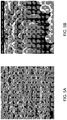
- FIGS. 5A-5B illustrates a SEM image of an approximately 100 nanometer aluminum oxide layer coated on a 25 micron polymeric separator according to implementations described herein.
- the columnar structure of the aluminum oxide dielectric layer is visible in FIG. 5B .
- Adhesion between the polyolefinic layer and the aluminum oxide layer is also visible.
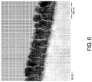
- FIG. 6 illustrates a TEM image of an approximately 100 nanometer coated on a 25 micron polymeric separator according to implementations described herein. The columnar structure and channels formed between the columns of aluminum oxide are also visible in FIG. 6 .
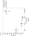
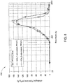
- FIG. 7 illustrates a plot 700 depicting charge-transfer resistance (R CT ) for monolayer and tri-layer separators with dielectric coating formed according to implementations described herein.
- the y-axis represents charge-transfer resistance (R CT ).
- the x-axis represents the thickness of the aluminum oxide layer (35 nanometers, 147 nanometers, and 172 nanometers) formed on both monolayer and tri-layer separators. A control without any aluminum oxide coating was also used.
- Monolayer separators were used for the 35 nanometer and control.
- Tri-layer separators were used for the 147 nanometer and 172 nanometer examples.
- the R CT for all three of the dielectric coated separators is lower than the R CT for the uncoated separator.
- Impedance spectra analysis of coin cells is depicted in Table II.
- Table II. Li/2 separator_1M LiPF 6 in EC:EMC 1:3, 2%VC/Li coin cell Control ⁇ 35 nm AlO x 147 nm AlO x 500 nm AlO x Room Temperature Ionic Conductivity (S/cm) 3.30 x 10 -3 1.78 x 10 -3 14.3 x 10 -3 13.0 x 10 -3 Charge Transfer Resistance (Ohm_cm 2 ) 417.4 190.6 67.3 46.6
- Thermal shrinkage results are depicted in Table III and Table IV.
- WD is the web direction and TD is the transverse direction.
- the thermal shrinkage test was performed using 2 x 2 cm square cut-outs of separator material with a dielectric coating deposited according to the implementations described herein.
- Exemplary separator materials include Celgard® PP2075 (20 um microporous monolayer PP membrane), Celgard® PP1615 (16 um microporous monolayer polyethylene membrane), Celgard® 2320 (20 um microporous trilayer membrane (PP/PE/PP)), and Celgard® C210 (16 um microporous trilayer membrane (PP/PE/PP)).
- Results achieved include: (1) Uniform 30 nm and 175 nm thick AlOx coating was completed using Al evaporation in reactive oxygen environment on porous polyolefin separator of 40 cm wide, 400-800 meters long web, (thickness 16 um, 20 um and 25 um) with corona surface treatment (2) The AlO x coating adhesion seems to be good with scotch tape peeling tests (3) the wettability of AlO x coated separator is better than uncoated separator (4) the Li symmetric cells showed 2x reduction in charge transfer resistance compared to control indicating that dielectric coating pores offer least resistance and (5) SEM cross section image showed columnar AlO x structure and crystallites are aligned vertically on the porous separator substrate.
- Table V and Table VI depict the Brunauer-Emmett-Teller (BET) Surface Area Analysis and Barrett-Joyner-Halenda (BJH) Pore Size and Volume Analysis determined using test method ISO 15901-2:2006 for a Celgard® PP1615 separator having a thickness of 16 ⁇ m.
- BET analysis provides surface area evaluation of materials by nitrogen multilayer adsorption measured as a function of relative pressure using a fully automated analyzer.
- BET techniques encompass external area and pore area evaluations to determine the total specific surface area in m 2 /g yielding information about surface porosity.
- BJH techniques are also employed to determine pore area and pore volume with 4V/A pore diameter using adsorption and desorption techniques.
- FIG. 8 illustrates a plot 800 depicting pore size distribution based on Barrett-Joyner-Halenda analysis for a prior art separator verses a separator with ceramic coating according to implementations described herein.
- the pore size distribution is shown for an uncoated Celgard® PP1615 separator having a thickness of 16 ⁇ m, a Celgard® PP1615 separator having a thickness of 16 ⁇ m and coated on one surface with a ⁇ 250 nm AlOx coating according to implementations described herein, and a Celgard® PP1615 separator having a thickness of 16 ⁇ m and coated on two opposing surfaces with a ⁇ 200 nm AlOx coating according to implementations described herein.
- the substrate has a plurality of pores and the at least one dielectric layer does not block a majority of the pores. In some implementations, the substrate has a plurality of pores and the at least one dielectric layer does not block 60% or more of the pores. For example, in different implementations, the at least one dielectric layer does not block at least 50% or more, 55% or more, 60% or more, 65% or more, 70% or more, 75% or more, 80% or more, 85% or more, 90% or more, or within a range bounded by any two of these values.
- Table VII depicts an estimate of the unblocked pores for implementations of the present disclosure.
- the control substrates labeled as "Control” in the first column are uncoated separators.
- the second and third columns represent the width and length of the substrate/separator.
- the fourth column represents the mass of the substrate for the substrates labeled (Control) and the total mass of the substrate and the dielectric coating for the substrates coated according to the present disclosure.
- the percent of estimated pore unblocked in column 7 is based on the pore volume for the control versus a single layer dielectric coated sample. Table VII.
- FIG. 9 a process flow chart summarizing another implementation of a method 900 for forming an electrode structure according to implementations described herein.
- the method 900 may be used, for example, to form the coated separator 130 depicted in FIG. 2 .
- the method 900 is similar to the method 300 discussed above except that the dielectric material is formed directly on the surface of the anode, the surface of the cathode, or both the surface of the anode and the surface of the cathode.
- the material to be deposited on the surface of the positive electrode is evaporated.
- the evaporation process of block 910 may be performed similarly to the evaporation process of block 330 of method 300.
- a reactive gas is flowed into the processing region for reacting with the evaporated material to deposit dielectric material on at least a portion of a surface of the positive electrode.
- the process of block 920 may be performed similarly to the evaporation process of block 340 of method 300.
- the material to be deposited on the surface of the positive electrode is evaporated.
- the evaporation process of block 930 may be performed similarly to the evaporation process of block 330 of method 300.
- a reactive gas is flowed into the processing region for reacting with the evaporated material to deposit dielectric material on at least a portion of a surface of the negative electrode.
- the process of block 940 may be performed similarly to the evaporation process of block 340 of method 300.
- a dielectric polymer layer may be formed on the dielectric layer.
- the process of block 950 may be performed similarly to the process of block 360 of method 300.
- the positive electrode and the negative electrode are joined together with the dielectric material and a microporous ion conducting polymer substrate positioned therebetween.
- the electrode structure has a coated separator with a dielectric coating on opposing sides.
- the electrode structure has a separator with only one side coated with dielectric material.
Landscapes
- Chemical & Material Sciences (AREA)
- Chemical Kinetics & Catalysis (AREA)
- Electrochemistry (AREA)
- General Chemical & Material Sciences (AREA)
- Engineering & Computer Science (AREA)
- Materials Engineering (AREA)
- Power Engineering (AREA)
- Manufacturing & Machinery (AREA)
- Inorganic Chemistry (AREA)
- Microelectronics & Electronic Packaging (AREA)
- Ceramic Engineering (AREA)
- Composite Materials (AREA)
- Cell Separators (AREA)
- Secondary Cells (AREA)
- Electric Double-Layer Capacitors Or The Like (AREA)
- Cell Electrode Carriers And Collectors (AREA)
- Battery Electrode And Active Subsutance (AREA)
Applications Claiming Priority (3)
| Application Number | Priority Date | Filing Date | Title |
|---|---|---|---|
| US201562171313P | 2015-06-05 | 2015-06-05 | |
| US14/937,442 US9508976B2 (en) | 2015-01-09 | 2015-11-10 | Battery separator with dielectric coating |
| PCT/US2016/034579 WO2016196264A1 (en) | 2015-06-05 | 2016-05-27 | Battery separator with dielectric coating |
Publications (3)
| Publication Number | Publication Date |
|---|---|
| EP3304617A1 EP3304617A1 (en) | 2018-04-11 |
| EP3304617A4 EP3304617A4 (en) | 2018-12-19 |
| EP3304617B1 true EP3304617B1 (en) | 2020-09-02 |
Family
ID=57441711
Family Applications (1)
| Application Number | Title | Priority Date | Filing Date |
|---|---|---|---|
| EP16804102.8A Active EP3304617B1 (en) | 2015-06-05 | 2016-05-27 | Battery separator with dielectric coating |
Country Status (6)
| Country | Link |
|---|---|
| EP (1) | EP3304617B1 (enExample) |
| JP (1) | JP6768713B2 (enExample) |
| KR (3) | KR102593300B1 (enExample) |
| CN (2) | CN107710453B (enExample) |
| TW (2) | TWI714829B (enExample) |
| WO (1) | WO2016196264A1 (enExample) |
Cited By (1)
| Publication number | Priority date | Publication date | Assignee | Title |
|---|---|---|---|---|
| EP3841631A4 (en) * | 2018-08-21 | 2022-03-30 | Applied Materials, Inc. | ULTRA-THIN CERAMIC COATING ON A BATTERY SEPARATOR |
Families Citing this family (10)
| Publication number | Priority date | Publication date | Assignee | Title |
|---|---|---|---|---|
| WO2019036137A1 (en) * | 2017-08-17 | 2019-02-21 | Applied Materials, Inc. | LI-ION BATTERY WITHOUT OLEFIN SEPARATOR |
| CN109994691B (zh) | 2017-12-29 | 2021-09-21 | 宁德时代新能源科技股份有限公司 | 一种隔离膜,其制备方法及包括该隔离膜的电化学装置 |
| CN108761949B (zh) * | 2018-05-29 | 2020-11-10 | 中国科学院上海硅酸盐研究所 | 一种固态离子传导层及含该固态离子传导层的固态电致变色器件 |
| CN110660948B (zh) * | 2018-06-29 | 2022-06-10 | 宁德时代新能源科技股份有限公司 | 一种隔离膜及其制备方法和含有该隔离膜的电化学装置 |
| CN109167002A (zh) * | 2018-08-15 | 2019-01-08 | 合肥国轩高科动力能源有限公司 | 一种锂硫电池复合隔膜的制备方法 |
| JP7142770B2 (ja) * | 2018-09-07 | 2022-09-27 | アプライド マテリアルズ インコーポレイテッド | バッテリ用セパレータへのセラミックコーティング |
| TWI686978B (zh) | 2018-12-28 | 2020-03-01 | 財團法人工業技術研究院 | 金屬離子電池 |
| CN112038546A (zh) * | 2019-06-03 | 2020-12-04 | 河北金力新能源科技股份有限公司 | 一种锂硫电池功能隔膜、制备方法及应用和锂硫电池 |
| US11721801B2 (en) * | 2020-08-17 | 2023-08-08 | International Business Machines Corporation, Armonk | Low resistance composite silicon-based electrode |
| CN115473007B (zh) * | 2022-09-28 | 2024-01-02 | 上海意定新材料科技有限公司 | 一种新能源汽车锂电池用陶瓷基隔膜及其制备方法 |
Family Cites Families (26)
| Publication number | Priority date | Publication date | Assignee | Title |
|---|---|---|---|---|
| JPH0636800A (ja) * | 1992-07-17 | 1994-02-10 | Mitsubishi Cable Ind Ltd | リチウム二次電池 |
| WO2001039303A1 (en) * | 1999-11-23 | 2001-05-31 | Moltech Corporation | Lithium anodes for electrochemical cells |
| US6432586B1 (en) | 2000-04-10 | 2002-08-13 | Celgard Inc. | Separator for a high energy rechargeable lithium battery |
| JP2002231221A (ja) * | 2001-02-01 | 2002-08-16 | Mitsubishi Heavy Ind Ltd | リチウム二次電池用電極又はセパレータ及びこれらの製造方法並びにこれらを用いたリチウム二次電池 |
| US7070632B1 (en) * | 2001-07-25 | 2006-07-04 | Polyplus Battery Company | Electrochemical device separator structures with barrier layer on non-swelling membrane |
| US6911280B1 (en) * | 2001-12-21 | 2005-06-28 | Polyplus Battery Company | Chemical protection of a lithium surface |
| MX268289B (es) * | 2002-10-15 | 2009-07-14 | Polyplus Battery Co Inc | Compuestos conductores ionicamente para la proteccion de anodos metalicos activos. |
| KR100467705B1 (ko) * | 2002-11-02 | 2005-01-24 | 삼성에스디아이 주식회사 | 무기 보호막을 갖는 세퍼레이타 및 이를 채용한 리튬 전지 |
| KR101043935B1 (ko) * | 2003-09-26 | 2011-06-29 | 쇼와 덴코 가부시키가이샤 | 콘덴서의 제조방법 |
| JP4529436B2 (ja) * | 2003-12-19 | 2010-08-25 | パナソニック株式会社 | リチウムイオン二次電池用極板およびリチウムイオン二次電池 |
| JP4839117B2 (ja) * | 2005-04-04 | 2011-12-21 | パナソニック株式会社 | 円筒型リチウム二次電池 |
| DE102005042215A1 (de) * | 2005-09-05 | 2007-03-08 | Degussa Ag | Separator mit verbesserter Handhabbarkeit |
| TW201415551A (zh) * | 2006-03-31 | 2014-04-16 | Applied Materials Inc | 用以改良介電薄膜之階梯覆蓋與圖案負載的方法 |
| JP4899793B2 (ja) * | 2006-10-31 | 2012-03-21 | パナソニック株式会社 | 真空蒸着装置 |
| TW200919803A (en) * | 2007-06-07 | 2009-05-01 | Koninkl Philips Electronics Nv | Solid-state battery and method for manufacturing of such a solid-state battery |
| WO2009081594A1 (ja) * | 2007-12-26 | 2009-07-02 | Panasonic Corporation | 非水電解質二次電池 |
| US8486562B2 (en) * | 2009-02-25 | 2013-07-16 | Applied Materials, Inc. | Thin film electrochemical energy storage device with three-dimensional anodic structure |
| EP2530183A4 (en) * | 2010-01-26 | 2015-11-18 | Panasonic Ip Man Co Ltd | DEVICE FOR PRODUCING A THIN LAYER, METHOD FOR PRODUCING A THIN LAYER AND SUBSTRATE CONVEYING ROLLERS |
| KR20120039334A (ko) * | 2010-10-15 | 2012-04-25 | 성균관대학교산학협력단 | 전기화학소자용 분리막 및 이의 제조방법 |
| JP5682372B2 (ja) * | 2011-02-07 | 2015-03-11 | ソニー株式会社 | 電池用セパレータ、電池用セパレータの製造方法、電池、電池パックおよび電子機器 |
| CN102244223A (zh) * | 2011-05-26 | 2011-11-16 | 东莞新能源科技有限公司 | 电化学装置及其无机/有机复合多孔性薄膜 |
| JP5429436B2 (ja) | 2011-11-29 | 2014-02-26 | パナソニック株式会社 | コンデンサ |
| CN104115325B (zh) * | 2012-01-24 | 2017-02-22 | 艾诺维克斯公司 | 用于能量存储装置的离子透过结构 |
| KR101683212B1 (ko) | 2012-02-07 | 2016-12-06 | 삼성에스디아이 주식회사 | 리튬 이차 전지의 제조 방법 |
| TWI478185B (zh) * | 2013-03-12 | 2015-03-21 | Univ Nat Taiwan | 超級電容器及其製造方法 |
| JP2015073015A (ja) * | 2013-10-03 | 2015-04-16 | パナソニックIpマネジメント株式会社 | 電極箔、電解コンデンサおよび電極箔の製造方法 |
-
2016
- 2016-05-27 EP EP16804102.8A patent/EP3304617B1/en active Active
- 2016-05-27 CN CN201680032907.3A patent/CN107710453B/zh active Active
- 2016-05-27 CN CN202011373938.XA patent/CN112599927B/zh active Active
- 2016-05-27 JP JP2017563067A patent/JP6768713B2/ja active Active
- 2016-05-27 WO PCT/US2016/034579 patent/WO2016196264A1/en not_active Ceased
- 2016-05-27 KR KR1020187000407A patent/KR102593300B1/ko active Active
- 2016-05-27 KR KR1020237035866A patent/KR102761680B1/ko active Active
- 2016-05-27 KR KR1020257002757A patent/KR20250039990A/ko active Pending
- 2016-06-03 TW TW107105174A patent/TWI714829B/zh active
- 2016-06-03 TW TW105117501A patent/TWI714594B/zh active
Non-Patent Citations (1)
| Title |
|---|
| None * |
Cited By (1)
| Publication number | Priority date | Publication date | Assignee | Title |
|---|---|---|---|---|
| EP3841631A4 (en) * | 2018-08-21 | 2022-03-30 | Applied Materials, Inc. | ULTRA-THIN CERAMIC COATING ON A BATTERY SEPARATOR |
Also Published As
| Publication number | Publication date |
|---|---|
| JP6768713B2 (ja) | 2020-10-14 |
| EP3304617A1 (en) | 2018-04-11 |
| CN107710453A (zh) | 2018-02-16 |
| TW201709590A (zh) | 2017-03-01 |
| CN107710453B (zh) | 2020-12-22 |
| TWI714829B (zh) | 2021-01-01 |
| KR102593300B1 (ko) | 2023-10-25 |
| KR102761680B1 (ko) | 2025-02-04 |
| TW201820678A (zh) | 2018-06-01 |
| EP3304617A4 (en) | 2018-12-19 |
| KR20250039990A (ko) | 2025-03-21 |
| WO2016196264A1 (en) | 2016-12-08 |
| JP2018523263A (ja) | 2018-08-16 |
| KR20230149342A (ko) | 2023-10-26 |
| TWI714594B (zh) | 2021-01-01 |
| KR20180006494A (ko) | 2018-01-17 |
| CN112599927A (zh) | 2021-04-02 |
| CN112599927B (zh) | 2023-01-13 |
Similar Documents
| Publication | Publication Date | Title |
|---|---|---|
| US12057574B2 (en) | Method of forming an anode structure with dielectric coating | |
| US11631922B2 (en) | Olefin separator free Li-ion battery | |
| EP3304617B1 (en) | Battery separator with dielectric coating | |
| US20230170581A1 (en) | Ultra-thin ceramic coating on separator for batteries |
Legal Events
| Date | Code | Title | Description |
|---|---|---|---|
| STAA | Information on the status of an ep patent application or granted ep patent |
Free format text: STATUS: THE INTERNATIONAL PUBLICATION HAS BEEN MADE |
|
| PUAI | Public reference made under article 153(3) epc to a published international application that has entered the european phase |
Free format text: ORIGINAL CODE: 0009012 |
|
| STAA | Information on the status of an ep patent application or granted ep patent |
Free format text: STATUS: REQUEST FOR EXAMINATION WAS MADE |
|
| 17P | Request for examination filed |
Effective date: 20171211 |
|
| AK | Designated contracting states |
Kind code of ref document: A1 Designated state(s): AL AT BE BG CH CY CZ DE DK EE ES FI FR GB GR HR HU IE IS IT LI LT LU LV MC MK MT NL NO PL PT RO RS SE SI SK SM TR |
|
| AX | Request for extension of the european patent |
Extension state: BA ME |
|
| DAV | Request for validation of the european patent (deleted) | ||
| DAX | Request for extension of the european patent (deleted) | ||
| A4 | Supplementary search report drawn up and despatched |
Effective date: 20181120 |
|
| RIC1 | Information provided on ipc code assigned before grant |
Ipc: H01M 2/16 20060101AFI20181114BHEP Ipc: H01M 4/66 20060101ALI20181114BHEP Ipc: H01M 2/14 20060101ALI20181114BHEP Ipc: H01M 10/052 20100101ALI20181114BHEP Ipc: H01G 11/52 20130101ALI20181114BHEP Ipc: H01M 10/0525 20100101ALI20181114BHEP Ipc: H01G 9/02 20060101ALI20181114BHEP |
|
| RIC1 | Information provided on ipc code assigned before grant |
Ipc: H01M 10/052 20100101ALI20200130BHEP Ipc: H01G 9/02 20060101ALI20200130BHEP Ipc: H01M 10/0525 20100101ALI20200130BHEP Ipc: H01M 4/66 20060101ALI20200130BHEP Ipc: H01M 2/16 20060101AFI20200130BHEP Ipc: H01G 11/52 20130101ALI20200130BHEP Ipc: H01M 2/14 20060101ALI20200130BHEP |
|
| GRAP | Despatch of communication of intention to grant a patent |
Free format text: ORIGINAL CODE: EPIDOSNIGR1 |
|
| STAA | Information on the status of an ep patent application or granted ep patent |
Free format text: STATUS: GRANT OF PATENT IS INTENDED |
|
| INTG | Intention to grant announced |
Effective date: 20200324 |
|
| GRAS | Grant fee paid |
Free format text: ORIGINAL CODE: EPIDOSNIGR3 |
|
| GRAA | (expected) grant |
Free format text: ORIGINAL CODE: 0009210 |
|
| STAA | Information on the status of an ep patent application or granted ep patent |
Free format text: STATUS: THE PATENT HAS BEEN GRANTED |
|
| AK | Designated contracting states |
Kind code of ref document: B1 Designated state(s): AL AT BE BG CH CY CZ DE DK EE ES FI FR GB GR HR HU IE IS IT LI LT LU LV MC MK MT NL NO PL PT RO RS SE SI SK SM TR |
|
| REG | Reference to a national code |
Ref country code: GB Ref legal event code: FG4D |
|
| REG | Reference to a national code |
Ref country code: AT Ref legal event code: REF Ref document number: 1309848 Country of ref document: AT Kind code of ref document: T Effective date: 20200915 Ref country code: CH Ref legal event code: EP |
|
| REG | Reference to a national code |
Ref country code: DE Ref legal event code: R096 Ref document number: 602016043345 Country of ref document: DE |
|
| REG | Reference to a national code |
Ref country code: IE Ref legal event code: FG4D |
|
| REG | Reference to a national code |
Ref country code: DE Ref legal event code: R079 Ref document number: 602016043345 Country of ref document: DE Free format text: PREVIOUS MAIN CLASS: H01M0002160000 Ipc: H01M0050409000 |
|
| REG | Reference to a national code |
Ref country code: LT Ref legal event code: MG4D |
|
| PG25 | Lapsed in a contracting state [announced via postgrant information from national office to epo] |
Ref country code: FI Free format text: LAPSE BECAUSE OF FAILURE TO SUBMIT A TRANSLATION OF THE DESCRIPTION OR TO PAY THE FEE WITHIN THE PRESCRIBED TIME-LIMIT Effective date: 20200902 Ref country code: HR Free format text: LAPSE BECAUSE OF FAILURE TO SUBMIT A TRANSLATION OF THE DESCRIPTION OR TO PAY THE FEE WITHIN THE PRESCRIBED TIME-LIMIT Effective date: 20200902 Ref country code: SE Free format text: LAPSE BECAUSE OF FAILURE TO SUBMIT A TRANSLATION OF THE DESCRIPTION OR TO PAY THE FEE WITHIN THE PRESCRIBED TIME-LIMIT Effective date: 20200902 Ref country code: GR Free format text: LAPSE BECAUSE OF FAILURE TO SUBMIT A TRANSLATION OF THE DESCRIPTION OR TO PAY THE FEE WITHIN THE PRESCRIBED TIME-LIMIT Effective date: 20201203 Ref country code: NO Free format text: LAPSE BECAUSE OF FAILURE TO SUBMIT A TRANSLATION OF THE DESCRIPTION OR TO PAY THE FEE WITHIN THE PRESCRIBED TIME-LIMIT Effective date: 20201202 Ref country code: LT Free format text: LAPSE BECAUSE OF FAILURE TO SUBMIT A TRANSLATION OF THE DESCRIPTION OR TO PAY THE FEE WITHIN THE PRESCRIBED TIME-LIMIT Effective date: 20200902 Ref country code: BG Free format text: LAPSE BECAUSE OF FAILURE TO SUBMIT A TRANSLATION OF THE DESCRIPTION OR TO PAY THE FEE WITHIN THE PRESCRIBED TIME-LIMIT Effective date: 20201202 |
|
| REG | Reference to a national code |
Ref country code: NL Ref legal event code: MP Effective date: 20200902 |
|
| REG | Reference to a national code |
Ref country code: AT Ref legal event code: MK05 Ref document number: 1309848 Country of ref document: AT Kind code of ref document: T Effective date: 20200902 |
|
| PG25 | Lapsed in a contracting state [announced via postgrant information from national office to epo] |
Ref country code: PL Free format text: LAPSE BECAUSE OF FAILURE TO SUBMIT A TRANSLATION OF THE DESCRIPTION OR TO PAY THE FEE WITHIN THE PRESCRIBED TIME-LIMIT Effective date: 20200902 Ref country code: LV Free format text: LAPSE BECAUSE OF FAILURE TO SUBMIT A TRANSLATION OF THE DESCRIPTION OR TO PAY THE FEE WITHIN THE PRESCRIBED TIME-LIMIT Effective date: 20200902 Ref country code: RS Free format text: LAPSE BECAUSE OF FAILURE TO SUBMIT A TRANSLATION OF THE DESCRIPTION OR TO PAY THE FEE WITHIN THE PRESCRIBED TIME-LIMIT Effective date: 20200902 |
|
| PG25 | Lapsed in a contracting state [announced via postgrant information from national office to epo] |
Ref country code: RO Free format text: LAPSE BECAUSE OF FAILURE TO SUBMIT A TRANSLATION OF THE DESCRIPTION OR TO PAY THE FEE WITHIN THE PRESCRIBED TIME-LIMIT Effective date: 20200902 Ref country code: PT Free format text: LAPSE BECAUSE OF FAILURE TO SUBMIT A TRANSLATION OF THE DESCRIPTION OR TO PAY THE FEE WITHIN THE PRESCRIBED TIME-LIMIT Effective date: 20210104 Ref country code: CZ Free format text: LAPSE BECAUSE OF FAILURE TO SUBMIT A TRANSLATION OF THE DESCRIPTION OR TO PAY THE FEE WITHIN THE PRESCRIBED TIME-LIMIT Effective date: 20200902 Ref country code: SM Free format text: LAPSE BECAUSE OF FAILURE TO SUBMIT A TRANSLATION OF THE DESCRIPTION OR TO PAY THE FEE WITHIN THE PRESCRIBED TIME-LIMIT Effective date: 20200902 Ref country code: EE Free format text: LAPSE BECAUSE OF FAILURE TO SUBMIT A TRANSLATION OF THE DESCRIPTION OR TO PAY THE FEE WITHIN THE PRESCRIBED TIME-LIMIT Effective date: 20200902 |
|
| PG25 | Lapsed in a contracting state [announced via postgrant information from national office to epo] |
Ref country code: AT Free format text: LAPSE BECAUSE OF FAILURE TO SUBMIT A TRANSLATION OF THE DESCRIPTION OR TO PAY THE FEE WITHIN THE PRESCRIBED TIME-LIMIT Effective date: 20200902 Ref country code: AL Free format text: LAPSE BECAUSE OF FAILURE TO SUBMIT A TRANSLATION OF THE DESCRIPTION OR TO PAY THE FEE WITHIN THE PRESCRIBED TIME-LIMIT Effective date: 20200902 Ref country code: ES Free format text: LAPSE BECAUSE OF FAILURE TO SUBMIT A TRANSLATION OF THE DESCRIPTION OR TO PAY THE FEE WITHIN THE PRESCRIBED TIME-LIMIT Effective date: 20200902 Ref country code: IS Free format text: LAPSE BECAUSE OF FAILURE TO SUBMIT A TRANSLATION OF THE DESCRIPTION OR TO PAY THE FEE WITHIN THE PRESCRIBED TIME-LIMIT Effective date: 20210102 |
|
| REG | Reference to a national code |
Ref country code: DE Ref legal event code: R097 Ref document number: 602016043345 Country of ref document: DE |
|
| PG25 | Lapsed in a contracting state [announced via postgrant information from national office to epo] |
Ref country code: SK Free format text: LAPSE BECAUSE OF FAILURE TO SUBMIT A TRANSLATION OF THE DESCRIPTION OR TO PAY THE FEE WITHIN THE PRESCRIBED TIME-LIMIT Effective date: 20200902 |
|
| PLBE | No opposition filed within time limit |
Free format text: ORIGINAL CODE: 0009261 |
|
| STAA | Information on the status of an ep patent application or granted ep patent |
Free format text: STATUS: NO OPPOSITION FILED WITHIN TIME LIMIT |
|
| 26N | No opposition filed |
Effective date: 20210603 |
|
| PG25 | Lapsed in a contracting state [announced via postgrant information from national office to epo] |
Ref country code: DK Free format text: LAPSE BECAUSE OF FAILURE TO SUBMIT A TRANSLATION OF THE DESCRIPTION OR TO PAY THE FEE WITHIN THE PRESCRIBED TIME-LIMIT Effective date: 20200902 Ref country code: SI Free format text: LAPSE BECAUSE OF FAILURE TO SUBMIT A TRANSLATION OF THE DESCRIPTION OR TO PAY THE FEE WITHIN THE PRESCRIBED TIME-LIMIT Effective date: 20200902 |
|
| PG25 | Lapsed in a contracting state [announced via postgrant information from national office to epo] |
Ref country code: IT Free format text: LAPSE BECAUSE OF FAILURE TO SUBMIT A TRANSLATION OF THE DESCRIPTION OR TO PAY THE FEE WITHIN THE PRESCRIBED TIME-LIMIT Effective date: 20200902 |
|
| REG | Reference to a national code |
Ref country code: CH Ref legal event code: PL |
|
| PG25 | Lapsed in a contracting state [announced via postgrant information from national office to epo] |
Ref country code: CH Free format text: LAPSE BECAUSE OF NON-PAYMENT OF DUE FEES Effective date: 20210531 Ref country code: LU Free format text: LAPSE BECAUSE OF NON-PAYMENT OF DUE FEES Effective date: 20210527 Ref country code: MC Free format text: LAPSE BECAUSE OF FAILURE TO SUBMIT A TRANSLATION OF THE DESCRIPTION OR TO PAY THE FEE WITHIN THE PRESCRIBED TIME-LIMIT Effective date: 20200902 Ref country code: LI Free format text: LAPSE BECAUSE OF NON-PAYMENT OF DUE FEES Effective date: 20210531 |
|
| REG | Reference to a national code |
Ref country code: BE Ref legal event code: MM Effective date: 20210531 |
|
| PG25 | Lapsed in a contracting state [announced via postgrant information from national office to epo] |
Ref country code: IE Free format text: LAPSE BECAUSE OF NON-PAYMENT OF DUE FEES Effective date: 20210527 |
|
| PG25 | Lapsed in a contracting state [announced via postgrant information from national office to epo] |
Ref country code: BE Free format text: LAPSE BECAUSE OF NON-PAYMENT OF DUE FEES Effective date: 20210531 |
|
| PG25 | Lapsed in a contracting state [announced via postgrant information from national office to epo] |
Ref country code: NL Free format text: LAPSE BECAUSE OF NON-PAYMENT OF DUE FEES Effective date: 20200923 Ref country code: CY Free format text: LAPSE BECAUSE OF FAILURE TO SUBMIT A TRANSLATION OF THE DESCRIPTION OR TO PAY THE FEE WITHIN THE PRESCRIBED TIME-LIMIT Effective date: 20200902 |
|
| PG25 | Lapsed in a contracting state [announced via postgrant information from national office to epo] |
Ref country code: HU Free format text: LAPSE BECAUSE OF FAILURE TO SUBMIT A TRANSLATION OF THE DESCRIPTION OR TO PAY THE FEE WITHIN THE PRESCRIBED TIME-LIMIT; INVALID AB INITIO Effective date: 20160527 |
|
| PG25 | Lapsed in a contracting state [announced via postgrant information from national office to epo] |
Ref country code: MK Free format text: LAPSE BECAUSE OF FAILURE TO SUBMIT A TRANSLATION OF THE DESCRIPTION OR TO PAY THE FEE WITHIN THE PRESCRIBED TIME-LIMIT Effective date: 20200902 |
|
| PG25 | Lapsed in a contracting state [announced via postgrant information from national office to epo] |
Ref country code: MT Free format text: LAPSE BECAUSE OF FAILURE TO SUBMIT A TRANSLATION OF THE DESCRIPTION OR TO PAY THE FEE WITHIN THE PRESCRIBED TIME-LIMIT Effective date: 20200902 |
|
| REG | Reference to a national code |
Ref country code: DE Ref legal event code: R081 Ref document number: 602016043345 Country of ref document: DE Owner name: ELEVATED MATERIALS GERMANY GMBH, DE Free format text: FORMER OWNER: APPLIED MATERIALS, INC., SANTA CLARA, CALIF., US |
|
| PGFP | Annual fee paid to national office [announced via postgrant information from national office to epo] |
Ref country code: DE Payment date: 20250423 Year of fee payment: 10 |
|
| PGFP | Annual fee paid to national office [announced via postgrant information from national office to epo] |
Ref country code: GB Payment date: 20250423 Year of fee payment: 10 |
|
| PGFP | Annual fee paid to national office [announced via postgrant information from national office to epo] |
Ref country code: FR Payment date: 20250423 Year of fee payment: 10 |