EP3291402B1 - Système permettant d'appliquer des champs èlectriques à de multiples panneaux solaires - Google Patents
Système permettant d'appliquer des champs èlectriques à de multiples panneaux solaires Download PDFInfo
- Publication number
- EP3291402B1 EP3291402B1 EP17192983.9A EP17192983A EP3291402B1 EP 3291402 B1 EP3291402 B1 EP 3291402B1 EP 17192983 A EP17192983 A EP 17192983A EP 3291402 B1 EP3291402 B1 EP 3291402B1
- Authority
- EP
- European Patent Office
- Prior art keywords
- voltage
- photovoltaic device
- switching means
- selected photovoltaic
- solar
- Prior art date
- Legal status (The legal status is an assumption and is not a legal conclusion. Google has not performed a legal analysis and makes no representation as to the accuracy of the status listed.)
- Active
Links
- 230000005684 electric field Effects 0.000 claims description 43
- 239000003990 capacitor Substances 0.000 claims description 14
- 230000001965 increasing effect Effects 0.000 claims description 6
- 238000002955 isolation Methods 0.000 claims description 5
- 230000007423 decrease Effects 0.000 claims description 3
- 230000004048 modification Effects 0.000 claims description 3
- 238000012986 modification Methods 0.000 claims description 3
- 230000000116 mitigating effect Effects 0.000 claims 1
- 238000010586 diagram Methods 0.000 description 19
- 238000000034 method Methods 0.000 description 12
- 238000009434 installation Methods 0.000 description 8
- 239000000969 carrier Substances 0.000 description 6
- 238000004146 energy storage Methods 0.000 description 6
- 238000003491 array Methods 0.000 description 5
- 239000002800 charge carrier Substances 0.000 description 5
- 238000004519 manufacturing process Methods 0.000 description 5
- 239000000463 material Substances 0.000 description 5
- 230000008569 process Effects 0.000 description 5
- XUIMIQQOPSSXEZ-UHFFFAOYSA-N Silicon Chemical compound [Si] XUIMIQQOPSSXEZ-UHFFFAOYSA-N 0.000 description 4
- 238000009792 diffusion process Methods 0.000 description 4
- 230000033001 locomotion Effects 0.000 description 4
- 230000006798 recombination Effects 0.000 description 4
- 238000005215 recombination Methods 0.000 description 4
- 229910052710 silicon Inorganic materials 0.000 description 4
- 239000010703 silicon Substances 0.000 description 4
- 230000001360 synchronised effect Effects 0.000 description 4
- 238000013459 approach Methods 0.000 description 3
- 230000002708 enhancing effect Effects 0.000 description 3
- 230000006872 improvement Effects 0.000 description 3
- 239000004065 semiconductor Substances 0.000 description 3
- 239000010409 thin film Substances 0.000 description 3
- 230000015556 catabolic process Effects 0.000 description 2
- 230000008878 coupling Effects 0.000 description 2
- 238000010168 coupling process Methods 0.000 description 2
- 238000005859 coupling reaction Methods 0.000 description 2
- 238000009413 insulation Methods 0.000 description 2
- 238000000926 separation method Methods 0.000 description 2
- 241000985284 Leuciscus idus Species 0.000 description 1
- 229910021417 amorphous silicon Inorganic materials 0.000 description 1
- 230000002238 attenuated effect Effects 0.000 description 1
- 230000008859 change Effects 0.000 description 1
- 238000010276 construction Methods 0.000 description 1
- 238000001816 cooling Methods 0.000 description 1
- 229910021419 crystalline silicon Inorganic materials 0.000 description 1
- 230000007812 deficiency Effects 0.000 description 1
- 230000001419 dependent effect Effects 0.000 description 1
- 230000003292 diminished effect Effects 0.000 description 1
- 230000000694 effects Effects 0.000 description 1
- 230000005611 electricity Effects 0.000 description 1
- 230000005686 electrostatic field Effects 0.000 description 1
- 230000001976 improved effect Effects 0.000 description 1
- 230000001939 inductive effect Effects 0.000 description 1
- 238000005259 measurement Methods 0.000 description 1
- 230000003287 optical effect Effects 0.000 description 1
- 230000005855 radiation Effects 0.000 description 1
- 230000000630 rising effect Effects 0.000 description 1
- 230000003068 static effect Effects 0.000 description 1
- 230000008093 supporting effect Effects 0.000 description 1
- 238000012360 testing method Methods 0.000 description 1
- 238000012549 training Methods 0.000 description 1
Images


Classifications
-
- H—ELECTRICITY
- H02—GENERATION; CONVERSION OR DISTRIBUTION OF ELECTRIC POWER
- H02S—GENERATION OF ELECTRIC POWER BY CONVERSION OF INFRARED RADIATION, VISIBLE LIGHT OR ULTRAVIOLET LIGHT, e.g. USING PHOTOVOLTAIC [PV] MODULES
- H02S40/00—Components or accessories in combination with PV modules, not provided for in groups H02S10/00 - H02S30/00
- H02S40/30—Electrical components
-
- H—ELECTRICITY
- H01—ELECTRIC ELEMENTS
- H01L—SEMICONDUCTOR DEVICES NOT COVERED BY CLASS H10
- H01L31/00—Semiconductor devices sensitive to infrared radiation, light, electromagnetic radiation of shorter wavelength or corpuscular radiation and specially adapted either for the conversion of the energy of such radiation into electrical energy or for the control of electrical energy by such radiation; Processes or apparatus specially adapted for the manufacture or treatment thereof or of parts thereof; Details thereof
- H01L31/02—Details
- H01L31/02002—Arrangements for conducting electric current to or from the device in operations
-
- H—ELECTRICITY
- H01—ELECTRIC ELEMENTS
- H01L—SEMICONDUCTOR DEVICES NOT COVERED BY CLASS H10
- H01L31/00—Semiconductor devices sensitive to infrared radiation, light, electromagnetic radiation of shorter wavelength or corpuscular radiation and specially adapted either for the conversion of the energy of such radiation into electrical energy or for the control of electrical energy by such radiation; Processes or apparatus specially adapted for the manufacture or treatment thereof or of parts thereof; Details thereof
- H01L31/02—Details
- H01L31/02016—Circuit arrangements of general character for the devices
- H01L31/02019—Circuit arrangements of general character for the devices for devices characterised by at least one potential jump barrier or surface barrier
- H01L31/02021—Circuit arrangements of general character for the devices for devices characterised by at least one potential jump barrier or surface barrier for solar cells
-
- H—ELECTRICITY
- H02—GENERATION; CONVERSION OR DISTRIBUTION OF ELECTRIC POWER
- H02J—CIRCUIT ARRANGEMENTS OR SYSTEMS FOR SUPPLYING OR DISTRIBUTING ELECTRIC POWER; SYSTEMS FOR STORING ELECTRIC ENERGY
- H02J1/00—Circuit arrangements for dc mains or dc distribution networks
- H02J1/10—Parallel operation of dc sources
- H02J1/12—Parallel operation of dc generators with converters, e.g. with mercury-arc rectifier
-
- H—ELECTRICITY
- H02—GENERATION; CONVERSION OR DISTRIBUTION OF ELECTRIC POWER
- H02J—CIRCUIT ARRANGEMENTS OR SYSTEMS FOR SUPPLYING OR DISTRIBUTING ELECTRIC POWER; SYSTEMS FOR STORING ELECTRIC ENERGY
- H02J3/00—Circuit arrangements for ac mains or ac distribution networks
- H02J3/38—Arrangements for parallely feeding a single network by two or more generators, converters or transformers
- H02J3/381—Dispersed generators
-
- H—ELECTRICITY
- H02—GENERATION; CONVERSION OR DISTRIBUTION OF ELECTRIC POWER
- H02J—CIRCUIT ARRANGEMENTS OR SYSTEMS FOR SUPPLYING OR DISTRIBUTING ELECTRIC POWER; SYSTEMS FOR STORING ELECTRIC ENERGY
- H02J3/00—Circuit arrangements for ac mains or ac distribution networks
- H02J3/38—Arrangements for parallely feeding a single network by two or more generators, converters or transformers
- H02J3/46—Controlling of the sharing of output between the generators, converters, or transformers
-
- H—ELECTRICITY
- H02—GENERATION; CONVERSION OR DISTRIBUTION OF ELECTRIC POWER
- H02J—CIRCUIT ARRANGEMENTS OR SYSTEMS FOR SUPPLYING OR DISTRIBUTING ELECTRIC POWER; SYSTEMS FOR STORING ELECTRIC ENERGY
- H02J7/00—Circuit arrangements for charging or depolarising batteries or for supplying loads from batteries
- H02J7/34—Parallel operation in networks using both storage and other dc sources, e.g. providing buffering
- H02J7/35—Parallel operation in networks using both storage and other dc sources, e.g. providing buffering with light sensitive cells
-
- H—ELECTRICITY
- H02—GENERATION; CONVERSION OR DISTRIBUTION OF ELECTRIC POWER
- H02S—GENERATION OF ELECTRIC POWER BY CONVERSION OF INFRARED RADIATION, VISIBLE LIGHT OR ULTRAVIOLET LIGHT, e.g. USING PHOTOVOLTAIC [PV] MODULES
- H02S40/00—Components or accessories in combination with PV modules, not provided for in groups H02S10/00 - H02S30/00
- H02S40/30—Electrical components
- H02S40/32—Electrical components comprising DC/AC inverter means associated with the PV module itself, e.g. AC modules
-
- H—ELECTRICITY
- H02—GENERATION; CONVERSION OR DISTRIBUTION OF ELECTRIC POWER
- H02S—GENERATION OF ELECTRIC POWER BY CONVERSION OF INFRARED RADIATION, VISIBLE LIGHT OR ULTRAVIOLET LIGHT, e.g. USING PHOTOVOLTAIC [PV] MODULES
- H02S40/00—Components or accessories in combination with PV modules, not provided for in groups H02S10/00 - H02S30/00
- H02S40/30—Electrical components
- H02S40/34—Electrical components comprising specially adapted electrical connection means to be structurally associated with the PV module, e.g. junction boxes
-
- H—ELECTRICITY
- H02—GENERATION; CONVERSION OR DISTRIBUTION OF ELECTRIC POWER
- H02S—GENERATION OF ELECTRIC POWER BY CONVERSION OF INFRARED RADIATION, VISIBLE LIGHT OR ULTRAVIOLET LIGHT, e.g. USING PHOTOVOLTAIC [PV] MODULES
- H02S40/00—Components or accessories in combination with PV modules, not provided for in groups H02S10/00 - H02S30/00
- H02S40/30—Electrical components
- H02S40/38—Energy storage means, e.g. batteries, structurally associated with PV modules
-
- H—ELECTRICITY
- H02—GENERATION; CONVERSION OR DISTRIBUTION OF ELECTRIC POWER
- H02J—CIRCUIT ARRANGEMENTS OR SYSTEMS FOR SUPPLYING OR DISTRIBUTING ELECTRIC POWER; SYSTEMS FOR STORING ELECTRIC ENERGY
- H02J2300/00—Systems for supplying or distributing electric power characterised by decentralized, dispersed, or local generation
- H02J2300/20—The dispersed energy generation being of renewable origin
- H02J2300/22—The renewable source being solar energy
- H02J2300/24—The renewable source being solar energy of photovoltaic origin
-
- Y—GENERAL TAGGING OF NEW TECHNOLOGICAL DEVELOPMENTS; GENERAL TAGGING OF CROSS-SECTIONAL TECHNOLOGIES SPANNING OVER SEVERAL SECTIONS OF THE IPC; TECHNICAL SUBJECTS COVERED BY FORMER USPC CROSS-REFERENCE ART COLLECTIONS [XRACs] AND DIGESTS
- Y02—TECHNOLOGIES OR APPLICATIONS FOR MITIGATION OR ADAPTATION AGAINST CLIMATE CHANGE
- Y02E—REDUCTION OF GREENHOUSE GAS [GHG] EMISSIONS, RELATED TO ENERGY GENERATION, TRANSMISSION OR DISTRIBUTION
- Y02E10/00—Energy generation through renewable energy sources
- Y02E10/50—Photovoltaic [PV] energy
- Y02E10/56—Power conversion systems, e.g. maximum power point trackers
-
- Y—GENERAL TAGGING OF NEW TECHNOLOGICAL DEVELOPMENTS; GENERAL TAGGING OF CROSS-SECTIONAL TECHNOLOGIES SPANNING OVER SEVERAL SECTIONS OF THE IPC; TECHNICAL SUBJECTS COVERED BY FORMER USPC CROSS-REFERENCE ART COLLECTIONS [XRACs] AND DIGESTS
- Y02—TECHNOLOGIES OR APPLICATIONS FOR MITIGATION OR ADAPTATION AGAINST CLIMATE CHANGE
- Y02E—REDUCTION OF GREENHOUSE GAS [GHG] EMISSIONS, RELATED TO ENERGY GENERATION, TRANSMISSION OR DISTRIBUTION
- Y02E70/00—Other energy conversion or management systems reducing GHG emissions
- Y02E70/30—Systems combining energy storage with energy generation of non-fossil origin
Definitions
- the present disclosure relates generally to photovoltaic devices and more specifically, but not exclusively, to systems and methods for maximizing the power or energy generated and the overall efficiency of one or more solar cells, for example, by applying and adjusting an external electric field across the solar cells.
- a solar cell also called a photovoltaic cell
- a solar cell is an electrical device that converts the energy of light directly into electricity by a process known as “the photovoltaic effect.” When exposed to light, the solar cell can generate and support an electric current without being attached to any external voltage source.
- the most common solar cell consists of a p-n junction 110 fabricated from semiconductor materials (e.g ., silicon), such as in a solar cell 100 shown in Fig. 1 .
- the p-n junction 110 includes a thin wafer consisting of an ultra-thin layer of n-type silicon on top of a thicker layer of p-type silicon. Where these two layers are in contact, an electrical field (not shown) is created near the top surface of the solar cell 100, and a diffusion of electrons occurs from the region of high electron concentration (the n-type side of the p-n junction 110) into the region of low electron concentration (the p-type side of the p-n junction 110).
- the p-n junction 110 is encapsulated between two conductive electrodes 101a, 101b.
- the top electrode 101a is either transparent to incident (solar) radiation or does not entirely cover the top of the solar cell 100.
- the electrodes 101a, 101b can serve as ohmic metal-semiconductor contacts that are connected to an external load 30 that is coupled in series. Although shown as resistive only, the load 30 can also include both resistive and reactive components.
- the photon When a photon hits the solar cell 100, the photon either: passes straight through the solar cell material-which generally happens for lower energy photons; reflects off the surface of the solar cell; or preferably is absorbed by the solar cell material-if the photon energy is higher than the silicon band gap-generating an electron-hole pair.
- the photon If the photon is absorbed, its energy is given to an electron in the solar cell material. Usually this electron is in the valence band and is tightly bound in covalent bonds between neighboring atoms, and hence unable to move far. The energy given to the electron by the photon "excites" the electron into the conduction band, where it is free to move around within the solar cell 100.
- the covalent bond that the electron was previously a part of now has one fewer electron-this is known as a hole.
- the presence of a missing covalent bond allows the bonded electrons of neighboring atoms to move into the hole, leaving another hole behind. In this way, a hole also can move effectively through the solar cell 100.
- photons absorbed in the solar cell 100 create mobile electron-hole pairs.
- the mobile electron-hole pair diffuses or drifts toward the electrodes 101a, 101b.
- the electron diffuses/drifts towards the negative electrode, and the hole diffuses/drifts towards the positive electrode.
- Diffusion of carriers e.g ., electrons
- the dominant mode of charge carrier separation is drifting, driven by the electrostatic field of the p-n junction 110 extending throughout the thickness of the thin film solar cell.
- the dominant mode of charge carrier separation is diffusion.
- the diffusion length of minor carriers i.e ., the length that photo-generated carriers can travel before they recombine) must be large in thicker solar cells.
- electrons that are created on the n-type side of the p-n junction 110, "collected" by the p-n junction 110, and swept onto the n-type side can provide power to the external load 30 (via the electrode 101a) and return to the p-type side (via the electrode 101b) of the solar cell 100.
- the electron can recombine with a hole that was either created as an electron-hole pair on the p-type side or swept across the p-n junction 110 from the n-type side.
- the electron-hole pair travels a circuitous route from the point the electron-hole pair is created to the point where the electron-hole pair is collected at the electrodes 101a, 101b. Since the path traveled by the electron-hole pair is long, ample opportunity exists for the electron or hole to recombine with another hole or electron, which recombination results in a loss of current to any external load 30. Stated in another way, when an electron-hole pair is created, one of the carriers may reach the p-n junction 110 (a collected carrier) and contribute to the current produced by the solar cell 100. Alternatively, the carrier can recombine with no net contribution to cell current. Charge recombination causes a drop in quantum efficiency (i.e ., the percentage of photons that are converted to electric current when the solar cell 100), and, therefore, the overall efficiency of the solar cell 100.
- quantum efficiency i.e ., the percentage of photons that are converted to electric current when the solar cell 100
- Recent attempts to reduce the cost and increase the efficiency of solar cells include testing various materials and different fabrication techniques used for the solar cells.
- Another approach attempts to enhance the depletion region formed around the p-n junction 110 for enhancing the movement of charge carriers through the solar cell 100.
- Hingorani Hingorani, et al.
- U.S. Patent 8,466,582 to Fornage
- Fornage Fornage
- Hingorani and Fornage disclose applying an external electric field to the solar cell using a modified solar cell structure.
- the application of the external electric field requires a voltage to be applied between electrodes inducing the electric field (described in further detail with reference to equation 2, below).
- applying the voltage to the existing electrodes 101a, 101b of the solar cell 100 shorts the applied voltage through the external load 30. Stated in another way, applying voltage to the electrodes 101a, 101b of the solar 100 is ineffective for creating an external electric field and enhancing the movement of charge carriers.
- the external electrodes must be placed on the solar cell 100 during the fabrication process-it is virtually impossible to retrofit the external electrodes to an existing solar cell or panel. This modification to the fabrication process significantly increases the cost of manufacturing and decreases the manufacturing yield. Additionally, placement of the external electrodes over the front, or incident side, of the solar cell 100 reduces the optical energy which reaches the solar cell 100, thereby yielding a lower power output.
- typical installation of the solar cell 100 can introduce additional factors-such as additional wiring, external hardware, and so on-that can affect the power output of the solar cell 100.
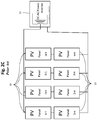
- multiple solar cells 100 can be coupled (in series and/or parallel) together to form a solar panel 10 (shown in Figs. 2A-D ).
- Each solar panel 10 can then be coupled using any suitable means described herein, including in parallel, series, or a combination thereof.
- Figs. 2A-D typical installation configurations using at least one solar panel 10 are shown.
- the solar panels 10 can be connected in either parallel ( Fig. 2A ), series ( Fig. 2B ), or a combination thereof ( Fig. 2C ).
- the solar panels 10 can drive a load, such as an inverter 31.
- Fig. 2A shows a series coupling of the solar panels 10.
- Fig. 2B shows the solar panels 10 are shown connected in series and drives the inverter 31.
- Fig. 2C shows an alternative installation of the solar panels 10 connected both in parallel and in series.
- Fig. 2D shows an installation-typically found in many residential installations-where each of the solar panels 10 are connected to its own inverter 31.
- Each method of connecting the solar cells 100 and the solar panels 10 requires different wiring and installation methods that change the electrical characteristics/behavior, and the corresponding power output, of the connected solar panels 10.
- Conventional efforts to increase the efficiency of solar cells rarely account for installation obstacles, such as the various methods for connecting multiple solar cells 100 and/or multiple solar panels 10.
- Document US 2012/006408 A1 discloses a method of operating a solar cell comprising: - for a solar cell having a single junction and first and second contacts, causing a bias across the first and second contacts to periodically alternate between minimum and maximum bias values; - the period of alternation of the bias between the minimum and maximum bias values being shorter than the hot carrier cooling time for the solar cell to extract from the solar cell, photo-excited carriers across a range of energy levels.
- Document US 2009/078304 A1 discloses that an external electric field is generated with a direction that is opposite to a polarity of a photovoltaic device, and applied to the photovoltaic device. Further, it is disclosed to apply the external electric field during a time when the photovoltaic device does not generate itself an electrical field (during night time where there is no sunlight).
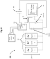
- a solar cell system that increases the mobility of electron-hole pairs and reduces the recombination current in a semiconductor material can prove desirable and provide a basis for a wide range of solar cell systems, such as to increase the efficiency and power output of solar cells configured as a solar panel. This result can be achieved, according to one embodiment disclosed herein, by a solar cell management system 300 as illustrated in Fig. 3 .
- the solar cell management system 300 is suitable for use with a wide range of photovoltaic devices.
- the solar cell management system 300 can be suitable for use with the solar cell 100 shown in Fig. 1 .
- the solar cell 100 can represent any suitable generation of solar cells such as wafer-based cells of crystalline silicon (first generation), thin film solar cells including amorphous silicon cells (second generation), and/or third generation cells.
- the solar cell management system 300 advantageously can be used with any generation of solar cell 100 without structural modification-and the associated drawbacks.
- the solar cell management system 300 can be suitable for use with multiple solar cells 100, such as the solar panels 10 shown in Figs. 2A-D .
- multiple solar cells 100 can be coupled (in series and/or parallel) together to form a solar panel 10.
- the solar panels 10 can be mounted on a supporting structure (not shown) via ground mounting, roof mounting, solar tracking systems, fixed racks, and so on and can be utilized for both terrestrial and space borne applications.
- the solar cell management system 300 advantageously can be used with any generation of solar panel 10 without structural modification-and the associated drawbacks-of the solar panel 10.
- the photovoltaic device 200 cooperates with an electric field 250.
- the polarity of the electric field 250 can be applied in either the same direction or the reverse direction as the polarity of the electrodes 101a, 101b (shown in Fig. 1 ) in the photovoltaic device 200.
- the electric field 250 acts on the electron-hole pairs in the photovoltaic device 200 to impose a force-e - E or h + E on the electron or hole, respectively-thereby accelerating the mobility of the electron and hole towards respective electrodes.
- the efficiency of the photovoltaic device 200 can be diminished as desired, such as for managing the power output of the photovoltaic device 200.
- the electric field 250 applied to the photovoltaic device 200 can be static or time varying as desired. In the case where the electric field 250 is time varying, the electric field 250 has a time averaged magnitude that is non-zero. Stated in another way, the net force on the electrons and holes is non-zero to provide increased mobility in the electron-hole pairs of the photovoltaic device 200.
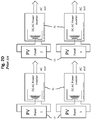
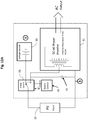
- the solar cell management system 300 can apply the external voltage V APP to the photovoltaic device 200 using any suitable means described herein, including using a switch 55 as shown in Fig. 4 .
- the photovoltaic device 200 can represent any number of photovoltaic devices such as the solar cell 100 and/or the solar panels 10 as illustrated.
- the solar panels 10 are shown to be wired in parallel (also shown in Fig. 2A ) and are connected to the switch 55, such as a single pole, double throw (or three-way) switch.
- the solar panels 10 also can be wired in series, a combination of series and parallel, and independently from one another.
- the switch 55 is also coupled to a voltage source 50 and an external load R L (e.g., shown as the inverter 31).
- the inverter 31 can include both resistive and reactive components.
- the inverter 31 can convert a DC voltage and current into an AC voltage and current, which is typically compatible in voltage and frequency with conventional AC power grids.
- the output frequency of the inverter 31 and the amplitude of the AC current/voltage can be based upon country, location, and local grid requirements.
- the voltage source 50 can include any suitable means for maintaining a constant voltage, including ideal voltage sources, controlled voltage sources, and so on. However, in some embodiments, the voltage source 50 can have a variable, adjustable output (e.g ., time varying voltage).
- a switch control (or controller) 45 is coupled to the switch 55 to control the duration of connection and/or the frequency of switching, such as between the voltage source 50 and the inverter 31 to the solar panels 10.
- the switch controller 45 can be preset to operate at a fixed switching duration D and switching frequency f .
- the magnitude of the voltage V App applied by voltage source 50, the duration D of connection, and/or the frequency f of switching can be preset and/or vary based on load conditions.
- the switch 55 connects the solar panels 10 with the voltage source 50 in a first position (as shown with the arrow in the switch 55 of Fig. 4 ).
- the voltage source 50 applies the voltage V APP across the electrodes 101a, 101b (shown in Fig. 1 ) of the solar panels 10 and induces the electric field 250 (shown in Fig. 3 ) across each solar panel 10.
- the switch 55 switches to connect the solar panels 10 to the inverter 31 (i.e ., the load R L ) in a second position.
- the voltage source 50 can provide the electric field 250 without being connected to the solar panels 10 and the inverter 31 at the same time. Therefore, applying the external voltage V APP does not allow the load R L ( e.g. , the inverter 31) to draw current directly from the voltage source 50.
- Application of the electric field 250 to the solar panels 10 can increase the current and power output of the solar panels 10 by a predetermined amount when the solar panels 10 subsequently are connected to the inverter 31 in the second position.
- the predetermined amount is dependent upon an intensity of light incident on the solar panels 10, the voltage applied V APP to the solar panels 10 by the voltage source 50, the thickness of the solar panels 10, the frequency f that the voltage source 50 is connected to the solar panels 10, and the duty cycle of the switching process between the first position and the second position-with the duty cycle being defined as the amount of time that the solar panels 10 are connected to the voltage source 50 divided by 1/ f the switching time ( i.e ., multiplied by the frequency f or divided by the total period of the signal).
- the switch duration time D, the switching frequency f , and the duty cycle are all interrelated quantities such that quantifying any two of the quantities allows for determination of the third quantity.
- specifying the switching frequency and the duty cycle allows for determination of the switch duration time D.
- the improvement in power output can be on the order of 20%; under low light conditions, 50+%.
- the embodiment shown in Fig. 4 advantageously provides the electric field 250 to the photovoltaic device 200 without the need to modify the solar panels 10 and/or solar cells 100 to include additional, external electrodes.
- an energy storage device such as a capacitor 41, an inductor 42, and/or a battery 43-can be placed before the inverter 31 to mitigate any voltage drop-out being seen by the inverter 31 while the switch 55 is in the first position. Accordingly, while the inverter 31 (i.e ., load) is disconnected from the solar panels 10 when the switch 55 is in the first position and the electric field 250 is being established across the solar panels 10, the energy storage device supplies energy to the inverter 31 to keep current flowing during this switched period. Stated in another way, the energy storage device can discharge while the solar panels 10 are disconnected from the inverter 31.
- duration switching times D of nominally 10-2000ns
- V App 's of nominally 100-500+ Volts
- a switching frequency f of 20 ⁇ seconds
- the duty cycle of nominally 0.1-10% can be used.
- the inductor 42, the capacitor 41, and/or the battery 43 are chosen to be of sufficient size to provide enough discharge while the solar panels 10 are disconnected while the electric field 250 is being placed across the solar panels 10 so as not to cause a drop out on the output of the inverter 31.
- Fig. 5 illustrates an alternative embodiment of the solar cell management system 300 of Fig. 3 .
- the photovoltaic device 200 can represent any number of photovoltaic devices such as the solar cell 100 and/or the solar panels 10 as illustrated.
- the solar panels 10 are wired in parallel (also shown in Fig. 2A ), but can also be wired in series and any combination thereof as will be discussed with reference to Figs. 13 and 15-17 .
- a voltage pulser 60 such as a high voltage pulse generator, can apply a time varying voltage pulse across one or more of the solar panels 10.
- a duration Dp of the voltage pulse can be short-nominally 10-2000 ns-and a magnitude can be high-nominally 100-500+ Volts.
- the voltages applied, the pulse width, and the pulse repetition rate are fixed at a predetermined level to provide optimum performance under selected operating conditions.
- the voltage pulse can have the duration D P of about 1000 ns, which voltage pulse is repeated with a period of 1/ f .
- the duration D P of the voltage pulse and the frequency f of the voltage pulse are chosen such that the reactance of inductors in the voltage inverter 31 present a high impedance to the voltage pulser 60, which high impedance allows a high voltage to be developed across the electrodes 101a, 101b (shown in Fig. 1 ) of the solar panels 10 and not be shorted out by the inverter 31.
- series inductors can be placed at the input of the inverter 31, which series inductors are capable of handling the current input to the inverter 31 and act as an RF choke such that the voltage pulses are not attenuated (or effectively shorted) by the resistive component of the inverter 31.
- the duty cycle time the pulse is on/time the pulse is off
- the strength of the electric field 250 imposed on the photovoltaic device 200 is a function of the construction of the photovoltaic device 200, such as the thickness of the photovoltaic device 200, the material and dielectric constant of the photovoltaic device 200, the maximum breakdown voltage of the photovoltaic device 200, and so on.
- the photovoltaic device 200 can include any number of solar cells 100 and/or solar panels 10, each solar cell 100 and solar panel 10, for example, being coupled in parallel, series, and/or a combination thereof.
- imposing the electric field 250 on a selected photovoltaic device 200 can account for the variations in configuration of the photovoltaic device 200.
- the solar cell management system 300 can apply the external voltage V App to the photovoltaic device 200.
- the solar cell management system 300 also can apply the external voltage V App to the solar panels 10 that are connected in series (shown in Fig. 2B ) and both series and parallel (shown in Fig. 2C ).
- the solar panels 10 are wired in series and connected to the switch 55, such as the single pole, double throw (or three-way) switch of Fig. 4 .
- the switch 55 is also coupled to the voltage source 50 and the external load R L ( e.g ., shown as the inverter 31).
- Equation 1 represents the upper and lower bounds of the applied external voltage V App .
- Equation 1 V P is the voltage output of the solar panel 10, and k is the kth panel in the configuration. As long the relationship among the applied external voltage V App and the minimum/maximum applied voltages of Equation 1 holds true, the switch 55 can the effectively apply the electric field 250 across each solar panel 10.
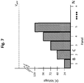
- Fig. 7 illustrates the external voltage V App relative to the voltage measured across each successive solar panel 10 (e.g ., from node A across nodes B, C...N) shown in Fig. 6 while the switch 55 is in the second position.
- the voltage across each solar panel 10 increases by the voltage output of the solar panel 10.
- each solar panel 10 generates a voltage of approximately twenty-four volts and that a voltage measured between the node A and any measurement node is approximately k x 24Volts, where k is the number of the solar panels 10 across which the voltage is being measured. If the inequality of the Equation 1 cannot be satisfied, the embodiment shown in Fig. 6 can be modified to include additional switches 55.
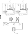
- a second switch 55 can be coupled into the series of the solar panels 10 as shown in Fig. 8 .
- more than one switch 55 i.e ., switch 55a, 55b...55n
- switch 55a, 55b...55n can be coupled to the solar panels 10 as desired.
- a toggle switch 72 can be added between the voltage source 50 and each group of k solar panels 10. To simplify the figures and for illustration purposes only, interconnections between different points in Fig. 8 are designated by the bordered capital letters A and B, where A couples to A and B couples to B.
- the toggle switch 72 can represent a single-pole, single throw (two-way) switch. Specifically, the toggle switch 72 can include N input ports and 1 output port. The toggle switch 72 further defines an ON state and an OFF state. In the ON state, all of the N input ports are simultaneously connected to the single output port. In the OFF state, none of the input ports are connected to the single output port.
- the toggle switch 72 can be activated by the switch controller 45, which also controls the switches 55a, 55b, and so on. As shown in Fig. 8 , the toggle switch 72 provides a return electrical path for the voltage source 50 when the switches 55a, 55b are in the first position (as discussed with reference to Fig. 4 ). The toggle switch 72 is activated (the ON state) when the switches 55a, 55 are connected to the voltage source 50 and the electric field 250 (shown in Fig. 3 ) is applied to the solar panels 10. The toggle switch 72 deactivates (the OFF state) while the solar panels 10 are providing power to the inverter 31.
- the switch control 45 can be synchronized such that switches 55a, 55b are placed in a first position simultaneously and connected to the voltage source 50, while the toggle switch 72 is concurrently activated in the ON state. Likewise, the switch controller 45 simultaneously places the switches 55a, 55b in the second position and also deactivates the toggle switch 72 (the OFF state).
- an energy storage device- such as the capacitor 41, the inductor 42, and/or the battery 43-can be placed before the inverter 31 to mitigate any voltage drop-out being seen by the inverter 31 while the switches 55a, 55b are in the first position.
- the solar cell management system 300 also can apply the external voltage V App to the solar panels 10 that are connected in parallel.
- more than one switch 55 can be controlled by the switch controller 45.
- each of the switches 55a, 55b can be synchronized by the switch controller 45 and are connected and disconnected simultaneously.
- an energy storage device-such as the capacitor 41, the inductor 42, and/or the battery 43- can be placed before the inverter 31 to mitigate any voltage drop-out being seen by the inverter 31 while the switches 55a, 55b are in the first position.
- the solar cell management system 300 also can apply the external voltage V App to the solar panels 10 that are connected in both series and parallel (shown in Fig. 2C ).
- V App the external voltage
- Fig. 10 two or more of the solar panels 10 are shown to be wired in series. The series wired solar panels 10 are then interconnected in parallel. The number of the solar panels 10 that are wired in series and in parallel can be preselected as desired.
- one or more switches 55 can be used to apply the electric field 250 (shown in Fig. 3 ) across the solar panels 10. If more than one switch 55 is used, the solar panels 10 can be wired as shown in Fig. 11 . Turning to Fig. 11 , the series wired solar panels 10 are wired in parallel and then interconnected to the switches 55a, 55b. In a preferred embodiment, the switch controller 45 synchronizes the switches 55a, 55b to be disconnected from the inverter 31 simultaneously. Similarly, the switch controller 45 connects both the switches 55a, 55b to the voltage source 50 at the same time.
- the solar cell management system 300 can cooperate with the solar panels typically found in many residential installations-where each of the solar panels 10 are connected to its own inverter 31 (shown in Fig. 2D ).
- the switch 55 can cooperate with each solar panel 10 in a number of ways.
- Fig. 12A illustrates the switch 55, the voltage source 50, and the switch controller 45 integrated into the inverter 31. Because the inverter 31 is typically connected to a power source, the capacitor 41 can be placed within the inverter 31.
- multiple solar panels 10 are typically used in combination and each are coupled to its own inverter 31 such that the capacitor 41 is not used.
- each inverter 31 operates independently of all other inverters 31 such that the switch 55 is not synchronized between inverters 31. Accordingly, a momentary drop out of power on a selected solar panel does not appreciably affect the quality of power from the plurality of solar panels 10 and inverters 31.
- each solar panel 10 and inverter 31 pair can include its own switch 55a-55n.
- Each switch 55 is connected to a central switch 46, which is controlled by a switch controller 72, and the voltage source 50.
- the central switch 46 can provide two concurrent outputs to each solar panel 10, each switch 55, and each inverter 31.
- the first output from the central switch 46 includes A1, B1...N1 and activates each switch 55 into the first position as discussed with reference to Fig. 4 .
- the external voltage V APP is applied from the voltage source 50 through the second output of the central switch 46, which includes A2, B2...N2.
- the switch controller 72 activates a selected switch 55, one at a time, through the central switch 46 and applies the external voltage V APP from the voltage source 50 to each of the solar panel 10 and inverter 31 pairs, serially. Since the duty cycle of each individual switch 55 is low-typically less than 2%-the switch controller 72 controls and drives a large number of switches 55, solar panels 10, and inverters 31.
- switch controller 72 there is no limitation on this embodiment that would preclude the switch controller 72 from switching and connecting the voltage source 50 to multiple solar panels 10 as long as the voltage applied to each panel is greater than the V min .
- more than one switch controller 72 can be added, with each switch controller 72 being responsible for a predetermined number of the solar panels 10.
- Each of the switch controllers 72 can behave independently.
- the solar cell management system 300 can also apply the external voltage V App to the photovoltaic device 200 using the voltage pulser 60 for a number of configurations of the solar panels 10.
- the voltage pulser circuit 60 is connected to the solar panels 10 wired in series.
- the voltage pulser 60 behaves as shown in Fig. 14.
- Fig. 14 illustrates the external voltage V App relative to the voltage across each successive solar panel 10 (measured across the node A to each of the solar panels 10 at the nodes B, C...N) in the series.
- the voltage at each solar panel 10 increases by the voltage output of the solar panel 10.
- each solar panel 10 generates a voltage of approximately twenty-four volts and that a voltage measured across any solar panel 10 (from the node A to the node B, C...N) is approximately k x 24Volts, where k is the number of solar panels 10 across which the voltage is being measured. If the inequality of the Equation 1 cannot be satisfied, the embodiment shown in Fig. 13 can be modified to include additional voltage pulsers 60.
- the solar management system 300 considers the DC voltage being generated by each of the solar cells 100 or the solar panels 10 themselves.
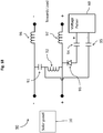
- a high voltage uplift circuit such as an Uplift Injector Circuit 90 (shown in Fig. 18 ) can be used with the voltage pulser 60 to superimpose a voltage pulse on top of the DC voltage of the solar panels 10 themselves. This superposition of the voltage pulse from the voltage pulser 60 on top of the DC voltage generated by solar panels 10 can be done by creating a negative reference for the injected high voltage pulse signal that is equal to the positive DC voltage delivered by solar panels 10.
- the Uplift Injector Circuit 90 includes a capacitor 91, working in concert with an inductor 92, allows the capacitor 91 to hold a charge equal to the voltage delivered by the solar panels 10.
- the capacitor 91 and the inductor 92 creates an uplifted negative reference for the injected high voltage pulse signal which is connected to the voltage pulser 60 through capacitors 94 and 95.
- the positive reference from the voltage pulser 60 is connected through a diode 93, which provides reverse bias protection to the positive voltage line connected to the interface that connects to the solar panels 10 and the interface which is connected to the inverter 31.
- inductors 96 and 97 can be placed in series between the inverter 31 and the voltage pulser 60 to provide a RF choke for any high voltage pulses.
- the inductors 96 and 97 attenuate any voltage pulse from the voltage pulser 60 passing across them and isolate the voltage pulser 60 from the remainder of the circuit towards the inverter 31.
- the inductor 92 provides high reactance protection to the injected high voltage pulse signal, keeping the signal from feeding back into the capacitor 91. The result is the injected high voltage pulse signal sitting on top of the DC voltage delivered by the solar panels 10 and rising and falling with the DC voltage, thereby maximizing the voltage pulse.
- the Uplift Injector Circuit 90 can be incorporated as part of an interface between each voltage pulser 60 and a number of solar panels 10.
- more than one voltage pulser 60 can be used for a predetermined number of solar panels 10 as shown in Figure 15A .
- the solar panels 10 are arranged in both in series and in parallel and interconnected with the voltage pulsers 60.
- Each voltage pulser 60 is responsible for k panels and interconnected to the inverter 31.
- the use of more than one voltage pulser 60 can be synchronized.
- the use of more than one voltage pulser 60 advantageously does not require synchronization between different voltage pulsers 60. Because the voltage pulse from each voltage pulser 60 is local to a set of the solar panels 10 that are interconnected, the application of the voltage pulse does not affect the output of the inverter 31.
- FIG. 15B Another embodiment of implementing multiple voltage pulsers for the solar panels 10 wired in series is shown in Fig. 15B .
- the voltage pulser 60 is connected to each solar panel 10 via a serial switch 70.
- the serial switch 70 can include N output ports for coupling k solar panels 10 as shown in Fig. 15B .
- interconnections between different points in the circuit are designated by the capital letters A1 and B1 with A1 connecting to A1 and B1 connecting to B1 and so on.
- the serial switch 70 includes one input port connected to the voltage pulser 60.
- the N output ports of the serial switch 70 connect the voltage pulser 60 across k panels 10 at a time.
- the serial switch 70 connects the voltage pulser 60 to the output ports A1 and A2.
- the voltage pulser 60 applies the external voltage V App across the solar panels 1 through k.
- the serial switch 70 disconnects the voltage pulser 60 from the outputs Aland A2 and connects the voltage pulser 60 to outputs B1 and B2.
- the voltage pulser 60 applies the voltage pulse V App across the k panels in that leg of the solar panels 10 wired in series.
- the serial switch 70 cycles through all ports applying the voltage pulse V App to k panels at a time.
- a single voltage pulser 60 can be utilized to apply voltage pulses V App to a large number of solar panels 10. Because the duty cycle of the voltage pulse is low-typically less than 2%-a single voltage pulser 60 can control multiple solar panels 10.
- the voltage pulser 60 cooperates with the solar panels 10 wired in both series and parallel in the manner discussed above with reference to Fig. 2C .
- the voltage pulser 60 is connected across the 2k solar panels 10 and the inverter 31.
- the magnitude of the series and shunt resistances >>1M ⁇ found in most solar panels 10 allow the voltage pulser 60 to cooperate with a large number of solar panels 10.
- Figs. 17A and 17B illustrates the voltage pulser 60 cooperating with the typical, residential installations of a solar panel 10.
- the voltage pulser 60 is integrated into the inverter 31 connected across solar panel 10.
- Fig. 17B illustrates an alternate embodiment for cooperating with the typical, residential installations of a solar panel 10 and includes each solar panel 10 and the inverter 31 connected via the serial switch 70 to a central voltage pulser 60.
- the central voltage pulser 60 applies the voltage pulse V App through the serial switch 70 and serially to each of the solar panels 10.
- the serial switch 70 in Figure 17b is shown as an Nx1 switch.
- the serial switch 70 has one input port, which is connected to the voltage pulser 60, and N output ports, which are connected across each individual solar panel 10 as shown in Figure 17b .
- the serial switch 70 connects voltage pulser 60 across each panel 10 one at a time.
- the serial switch 70 connects the voltage pulser 60 to the output ports A1 and A2. When activated, the voltage pulser 60 applies the voltage pulse V App across a selected solar panel 10 coupled to the serial switch 70. The serial switch 70 then disconnects the voltage pulser 60 from the output ports A1 and A2 and connects the voltage pulser 60 to the output ports B1 and B2. Again, when activated, the voltage pulser 60 applies the voltage pulse V App across another selected solar panel 10 coupled to the serial switch 70. In a like manner, the serial switch 70 cycles through all active ports applying a voltage pulse V App to a selected solar panel 10 at a time.
- a single voltage pulser 60 can be utilized to apply voltage pulses V App to a large number of solar panels 10. Since the duty cycle of the voltage pulses is very low, typically less than 2%, a single voltage pulser 60 can control a large number of the solar panels 10 and inverters 31.
- the central high voltage pulse generator precludes the central high voltage pulse generator from switching a voltage pulse to multiple solar panels concurrently as long as the voltage applied to each panel is greater than V min .
- the preferred embodiment includes a single voltage pulser 60 for switching between the solar panels 10, such as in serial. In the event that the number of the solar panels 10 becomes large, additional voltage pulsers 60 and serial switches 70 can be added, with each voltage pulser 60 responsible for a number of solar panels 10.
Landscapes
- Engineering & Computer Science (AREA)
- Power Engineering (AREA)
- Physics & Mathematics (AREA)
- Condensed Matter Physics & Semiconductors (AREA)
- Electromagnetism (AREA)
- General Physics & Mathematics (AREA)
- Computer Hardware Design (AREA)
- Microelectronics & Electronic Packaging (AREA)
- Life Sciences & Earth Sciences (AREA)
- Sustainable Development (AREA)
- Sustainable Energy (AREA)
- Photovoltaic Devices (AREA)
- Supply And Distribution Of Alternating Current (AREA)
- Inverter Devices (AREA)
- Power Sources (AREA)
- Charge And Discharge Circuits For Batteries Or The Like (AREA)
Claims (23)
- Système de gestion d'un ou plusieurs dispositifs photovoltaïques (200), comprenant :un moyen de commutation de tension (55) comprenant :un premier port activé pour être couplé à un dispositif photovoltaïque sélectionné (200) ;un deuxième port activé pour être couplé à une charge (RL, 31) commandée par le dispositif photovoltaïque sélectionné (200) ; etun troisième port activé pour être couplé à une source de tension (50),le moyen de commutation de tension (55) étant adapté pour fonctionner dans une première position pour fournir un premier chemin de courant entre le dispositif photovoltaïque sélectionné (200) et la source de tension (50) et une seconde position pour fournir un second chemin de courant entre le dispositif photovoltaïque sélectionné (200) et la charge (RL, 31), etun signal de tension généré par la source de tension (50) ayant la même polarité qu'une tension existante générée par le dispositif photovoltaïque (200), le signal de tension étant appliqué au dispositif photovoltaïque sélectionné (200) pour générer un champ électrique externe (250) à travers le dispositif photovoltaïque sélectionné (200) et pour être superposé à la tension existante générée par le dispositif photovoltaïque sélectionné pendant le fonctionnement du dispositif photovoltaïque lorsque le moyen de commutation de tension (55) est dans la première position, et une isolation électrique étant prévue entre la source de tension (50) et la charge (RL, 31) lorsque le moyen de commutation de tension (55) est dans la seconde position.
- Système selon la revendication 1, comprenant en outre :un second moyen de commutation de tension (55b) comprenant :un premier port activé pour être couplé à un second dispositif photovoltaïque sélectionné (200) ;un deuxième port activé pour être couplé à la charge (RL, 31), la charge (RL, 31) étant commandée par le dispositif photovoltaïque sélectionné (200) et le second dispositif photovoltaïque sélectionné (200) ; etun troisième port activé pour être couplé à la source de tension (50),le second moyen de commutation étant adapté pour fonctionner dans une première position pour fournir un premier chemin de courant entre le second dispositif photovoltaïque sélectionné (200) et la source de tension (50) et une seconde position pour fournir un second chemin de courant entre le second dispositif photovoltaïque sélectionné (200) et la charge (RL, 31), etle signal de tension généré par la source de tension (50) étant appliqué simultanément à la fois au dispositif photovoltaïque sélectionné (200) et au second dispositif photovoltaïque sélectionné (200), le premier état pour générer le champ électrique externe (250) à travers le dispositif photovoltaïque sélectionné (200) et le second dispositif photovoltaïque sélectionné (200) lorsque le moyen de commutation et le second moyen de commutation sont dans la première position, et le second état pour fournir une isolation électrique entre la source de tension (50) et la charge (RL, 31) lorsque le moyen de commutation et le second moyen de commutation sont dans la seconde position.
- Système selon la revendication 1 ou la revendication 2, au moins un du moyen de commutation de tension (55) et du second moyen de commutation de tension (55b) comprenant un interrupteur à double course.
- Système selon l'une quelconque des revendications 1 à 3, comprenant en outre un dispositif de commande de commutateur (45) couplé au moyen de commutation de tension (55), au moins l'une d'une fréquence et d'une durée de commutation entre la première position et la seconde position étant commandée par l'intermédiaire du dispositif de commande de commutateur.
- Système selon l'une quelconque des revendications 1 à 4, comprenant en outre un dispositif (42, 43) activé pour atténuer toute chute de tension du premier état à coupler entre la charge (RL, 31) et le dispositif photovoltaïque sélectionné (200).
- Système selon la revendication 5, le dispositif (42, 43) étant configuré pour fournir de l'énergie à la charge pendant que le moyen de commutation (55) est dans la première position.
- Système selon la revendication 6, le dispositif (42, 43) étant configuré pour stocker l'énergie générée par le dispositif photovoltaïque pendant que le moyen de commutation (55) est dans une seconde position.
- Système selon l'une quelconque des revendications 5 à 7, le dispositif (42, 43) comprenant un condensateur (41), une inductance (42) et/ou une batterie (43).
- Système selon l'une quelconque des revendications 1 à 8, le signal de tension généré par la source de tension (50) étant appliqué en tant que tension réglable au dispositif photovoltaïque sélectionné (200).
- Système selon l'une quelconque des revendications ci-dessus, le premier port dudit moyen de commutation de tension (55) étant activé pour être couplé à une pluralité de dispositifs photovoltaïques (200), le deuxième port dudit moyen de commutation de tension (55) étant activé pour être couplé à la charge (RL, 31) qui est commandée par la pluralité de dispositifs photovoltaïques (200), le premier état générant le champ électrique externe (250) à travers la pluralité de dispositifs photovoltaïques (200) lorsque le moyen de commutation de tension (55) est dans la première position.
- Système selon la revendication 10, les dispositifs photovoltaïques (200) étant disposés dans une configuration de dispositifs en série et/ou une configuration de dispositifs en parallèle.
- Système selon l'une quelconque des revendications 1 à 11, le premier état du signal de tension comprenant une série d'impulsions de tension (VApp) avec une amplitude positive pour générer le champ électrique externe (250) à travers le dispositif photovoltaïque sélectionné (200), et le second état du signal de tension comprenant un cycle d'arrêt entre des séries adjacentes d'impulsions de tension (VApp).
- Système selon la revendication 12, le signal de tension comprenant le second état entre des impulsions de tension adjacentes ou entre des impulsions de tension adjacentes sélectionnées.
- Système selon l'une quelconque des revendications 12 et 13, l'amplitude des impulsions de tension étant déterminée sur la base de la configuration de dispositif des dispositifs photovoltaïques (200).
- Système selon l'une quelconque des revendications 1 à 14, le champ électrique externe (250) étant généré avec une direction qui est la même que la polarité du dispositif photovoltaïque sélectionné (200) pour augmenter une puissance de sortie et/ou un courant de sortie du dispositif photovoltaïque sélectionné (200).
- Système selon la revendication 15, le moyen de commutation de tension (55) fournissant la puissance de sortie accrue et/ou le courant de sortie accru à la charge en seconde position.
- Système selon l'une quelconque des revendications 1 à 16, le champ électrique externe (250) étant généré avec une direction qui est opposée à une polarité du dispositif photovoltaïque sélectionné (200) pour diminuer une puissance de sortie et/ou un courant de sortie du dispositif photovoltaïque sélectionné (200).
- Système selon l'une quelconque des revendications ci-dessus, la charge (RL, 31) comprenant un onduleur (31) pour convertir une tension et/ou un courant continu (CC) généré par le dispositif photovoltaïque sélectionné (200) en une tension et/ou un courant alternatif (CA).
- Système selon l'une quelconque des revendications 1 à 18, le dispositif photovoltaïque sélectionné (200) étant électriquement isolé de la charge (RL, 31) dans le domaine des radiofréquences.
- Système selon la revendication 19, l'isolation électrique étant assurée par au moins une inductance (42, 92, 96, 97), au moins un condensateur (91), au moins une batterie (43) ou une combinaison de ceux-ci.
- Système selon l'une quelconque des revendications 1 à 20, le signal de tension étant appliqué au dispositif photovoltaïque sélectionné (200) sans modification structurelle du dispositif photovoltaïque sélectionné (200).
- Système selon la revendication 21, le signal de tension étant appliqué à des électrodes existantes (101a, 101b) du dispositif photovoltaïque sélectionné (200).
- Système selon l'une quelconque des revendications 1 à 22, ladite source de tension (50) appliquant le second état entre des premiers états adjacents sélectionnés, ou ladite source de tension (50) appliquant les premier et second états à chacun des dispositifs photovoltaïques (200).
Applications Claiming Priority (5)
| Application Number | Priority Date | Filing Date | Title |
|---|---|---|---|
| US201461947326P | 2014-03-03 | 2014-03-03 | |
| US201462022087P | 2014-07-08 | 2014-07-08 | |
| US14/628,079 US10069306B2 (en) | 2014-02-21 | 2015-02-20 | System and method for managing the power output of a photovoltaic cell |
| PCT/US2015/018552 WO2015134549A1 (fr) | 2014-03-03 | 2015-03-03 | Procédé et système permettant d'appliquer des champs électriques à de multiples panneaux solaires |
| EP15710361.5A EP3114746B1 (fr) | 2014-03-03 | 2015-03-03 | Procédé et système permettant d'appliquer des champs électriques à de multiples panneaux solaires |
Related Parent Applications (2)
| Application Number | Title | Priority Date | Filing Date |
|---|---|---|---|
| EP15710361.5A Division EP3114746B1 (fr) | 2014-03-03 | 2015-03-03 | Procédé et système permettant d'appliquer des champs électriques à de multiples panneaux solaires |
| EP15710361.5A Division-Into EP3114746B1 (fr) | 2014-03-03 | 2015-03-03 | Procédé et système permettant d'appliquer des champs électriques à de multiples panneaux solaires |
Publications (3)
| Publication Number | Publication Date |
|---|---|
| EP3291402A2 EP3291402A2 (fr) | 2018-03-07 |
| EP3291402A3 EP3291402A3 (fr) | 2018-03-21 |
| EP3291402B1 true EP3291402B1 (fr) | 2020-06-03 |
Family
ID=54055818
Family Applications (5)
| Application Number | Title | Priority Date | Filing Date |
|---|---|---|---|
| EP20162684.3A Pending EP3703217A1 (fr) | 2014-03-03 | 2015-03-03 | Procédé et système permettant d'appliquer des champs électriques à de multiples panneaux solaires |
| EP15710361.5A Active EP3114746B1 (fr) | 2014-03-03 | 2015-03-03 | Procédé et système permettant d'appliquer des champs électriques à de multiples panneaux solaires |
| EP16189404.3A Active EP3151358B1 (fr) | 2014-03-03 | 2015-03-03 | Procédé et système permettant d'appliquer des champs électriques à de multiples panneaux solaires |
| EP17192983.9A Active EP3291402B1 (fr) | 2014-03-03 | 2015-03-03 | Système permettant d'appliquer des champs èlectriques à de multiples panneaux solaires |
| EP17192984.7A Active EP3291403B8 (fr) | 2014-03-03 | 2015-03-03 | Système et procédé de gestion d'une pluralité de dispositifs photovoltaïques |
Family Applications Before (3)
| Application Number | Title | Priority Date | Filing Date |
|---|---|---|---|
| EP20162684.3A Pending EP3703217A1 (fr) | 2014-03-03 | 2015-03-03 | Procédé et système permettant d'appliquer des champs électriques à de multiples panneaux solaires |
| EP15710361.5A Active EP3114746B1 (fr) | 2014-03-03 | 2015-03-03 | Procédé et système permettant d'appliquer des champs électriques à de multiples panneaux solaires |
| EP16189404.3A Active EP3151358B1 (fr) | 2014-03-03 | 2015-03-03 | Procédé et système permettant d'appliquer des champs électriques à de multiples panneaux solaires |
Family Applications After (1)
| Application Number | Title | Priority Date | Filing Date |
|---|---|---|---|
| EP17192984.7A Active EP3291403B8 (fr) | 2014-03-03 | 2015-03-03 | Système et procédé de gestion d'une pluralité de dispositifs photovoltaïques |
Country Status (26)
| Country | Link |
|---|---|
| EP (5) | EP3703217A1 (fr) |
| JP (7) | JP6203422B2 (fr) |
| KR (8) | KR20210110889A (fr) |
| CN (6) | CN106105022B (fr) |
| AP (1) | AP2016009473A0 (fr) |
| AU (7) | AU2015227260B2 (fr) |
| BR (1) | BR112016019755B1 (fr) |
| CA (1) | CA2939004C (fr) |
| CL (3) | CL2016002210A1 (fr) |
| CY (1) | CY1121297T1 (fr) |
| DK (1) | DK3114746T3 (fr) |
| EA (2) | EA037717B1 (fr) |
| ES (4) | ES2665796T3 (fr) |
| HR (1) | HRP20180547T1 (fr) |
| HU (1) | HUE038571T2 (fr) |
| IL (6) | IL266125B (fr) |
| LT (1) | LT3114746T (fr) |
| MX (4) | MX362755B (fr) |
| NZ (1) | NZ722832A (fr) |
| PH (4) | PH12016501643A1 (fr) |
| PL (1) | PL3114746T3 (fr) |
| PT (1) | PT3114746T (fr) |
| RS (1) | RS57174B1 (fr) |
| SG (3) | SG10201912082PA (fr) |
| SI (1) | SI3114746T1 (fr) |
| WO (1) | WO2015134549A1 (fr) |
Families Citing this family (4)
| Publication number | Priority date | Publication date | Assignee | Title |
|---|---|---|---|---|
| IT201700060644A1 (it) * | 2017-06-01 | 2018-12-01 | Convert Tech S R L | Sistema per energizzare in corrente alternata carichi elettrici in un impianto fotovoltaico |
| RU2732183C1 (ru) * | 2019-12-09 | 2020-09-14 | Валентин Петрович Казанцев | Возобновляемый источник энергии |
| CN112820565B (zh) * | 2020-12-29 | 2021-11-30 | 常熟开关制造有限公司(原常熟开关厂) | 自动转换开关电器控制方法及自动转换开关电器 |
| CN116232215B (zh) * | 2023-05-10 | 2023-09-05 | 中国科学院过程工程研究所 | 一种光伏发电装置及方法 |
Family Cites Families (32)
| Publication number | Priority date | Publication date | Assignee | Title |
|---|---|---|---|---|
| US5215599A (en) | 1991-05-03 | 1993-06-01 | Electric Power Research Institute | Advanced solar cell |
| JP3206339B2 (ja) * | 1994-11-30 | 2001-09-10 | トヨタ自動車株式会社 | 太陽電池 |
| JPH0936402A (ja) * | 1995-07-21 | 1997-02-07 | Showa Shell Sekiyu Kk | 変換効率向上処理を施した薄膜太陽電池および変換 効率向上手段を付加した薄膜太陽電池アレイ |
| JPH10173215A (ja) * | 1996-12-16 | 1998-06-26 | Mitsubishi Electric Corp | 太陽電池融雪装置を具備した太陽光発電装置 |
| JP3781538B2 (ja) * | 1997-12-17 | 2006-05-31 | シャープ株式会社 | 太陽光発電装置 |
| JPH11233805A (ja) * | 1998-02-13 | 1999-08-27 | Nippon Telegr & Teleph Corp <Ntt> | 光電変換装置 |
| JPH11251615A (ja) * | 1998-03-03 | 1999-09-17 | Canon Inc | 融雪機能付き太陽光発電システム |
| JP4074748B2 (ja) * | 1998-09-03 | 2008-04-09 | マクロニクス インターナショナル カンパニー リミテッド | 浮遊ゲート・メモリ装置にトンネル電流を導入するために調節された電圧源 |
| JP2000323738A (ja) | 1999-05-14 | 2000-11-24 | Kanegafuchi Chem Ind Co Ltd | 太陽電池モジュールの逆バイアス処理装置 |
| AU766466B2 (en) * | 1999-05-14 | 2003-10-16 | Kaneka Corporation | Reverse biasing apparatus for solar battery module |
| AU2001252643A1 (en) * | 2000-08-07 | 2002-02-18 | Norio Akamatsu | Solar ray energy conversion apparatus |
| JP2004079997A (ja) * | 2002-06-19 | 2004-03-11 | Canon Inc | 発電システム及び発電装置 |
| DE102006023563B4 (de) * | 2006-05-19 | 2020-09-10 | Kostal Industrie Elektrik Gmbh | Photovoltaik-Anlage |
| US20090078304A1 (en) * | 2007-09-26 | 2009-03-26 | Jack Arthur Gilmore | Photovoltaic charge abatement device, system, and method |
| CA2737134C (fr) * | 2007-10-15 | 2017-10-10 | Ampt, Llc | Systemes pour energie solaire hautement efficace |
| KR20090128954A (ko) * | 2008-06-12 | 2009-12-16 | 주식회사 엔피홀딩스 | 태양전지 모듈 |
| US7969757B2 (en) * | 2008-12-12 | 2011-06-28 | Array Converter, Inc. | Apparatus providing bias to solar cells |
| EP2249457A1 (fr) * | 2009-05-08 | 2010-11-10 | Nxp B.V. | Cellule solaire PV |
| JP2011034942A (ja) | 2009-08-02 | 2011-02-17 | Michio Takaoka | 重畳電界の二次電池と太陽電池 |
| DE102010029813B4 (de) * | 2010-06-08 | 2023-02-23 | Sma Solar Technology Ag | Verfahren zur Steuerung einer elektrischen Stromerzeugung eines Submoduls in einer Photovoltaikanlage |
| US8217258B2 (en) * | 2010-07-09 | 2012-07-10 | Ostendo Technologies, Inc. | Alternating bias hot carrier solar cells |
| KR20120040016A (ko) * | 2010-10-18 | 2012-04-26 | 엘지전자 주식회사 | 태양 전지용 기판 및 태양 전지 |
| JP5912404B2 (ja) * | 2010-10-29 | 2016-04-27 | 株式会社半導体エネルギー研究所 | 光電変換装置 |
| US8466582B2 (en) | 2010-12-03 | 2013-06-18 | Enphase Energy, Inc. | Method and apparatus for applying an electric field to a photovoltaic element |
| KR101449891B1 (ko) * | 2011-05-20 | 2014-10-13 | 솔렉셀, 인크. | 태양 전지를 위한 자가-활성된 전면 바이어스 |
| DE102011115189A1 (de) * | 2011-09-28 | 2013-03-28 | Adensis Gmbh | PV-Anlage mit Sicherung gegen Einspeisung in ein öffentliches Stromversorgungsnetz |
| JP5819172B2 (ja) * | 2011-12-06 | 2015-11-18 | シャープ株式会社 | 電力供給システム |
| US9071191B2 (en) * | 2011-12-28 | 2015-06-30 | John L Patrick | Prefabricated solar array system |
| DE202012011176U1 (de) * | 2012-11-21 | 2013-03-28 | Karl-Heinz Prywerek | Elektrisches Feld als Unterstützung von Photovoltaikanlagen |
| CN103199131B (zh) * | 2013-04-11 | 2016-03-02 | 中国石油大学(华东) | 一种电场增强型肖特基结太阳能电池结构 |
| US10069306B2 (en) * | 2014-02-21 | 2018-09-04 | Solarlytics, Inc. | System and method for managing the power output of a photovoltaic cell |
| US10103547B2 (en) * | 2014-02-21 | 2018-10-16 | Solarlytics, Inc. | Method and system for applying electric fields to multiple solar panels |
-
2015
- 2015-03-03 IL IL266125A patent/IL266125B/en unknown
- 2015-03-03 SG SG10201912082PA patent/SG10201912082PA/en unknown
- 2015-03-03 CN CN201580012041.5A patent/CN106105022B/zh active Active
- 2015-03-03 KR KR1020217027069A patent/KR20210110889A/ko active IP Right Grant
- 2015-03-03 EA EA201891810A patent/EA037717B1/ru unknown
- 2015-03-03 SG SG11201607087SA patent/SG11201607087SA/en unknown
- 2015-03-03 KR KR1020197000365A patent/KR102089916B1/ko active IP Right Grant
- 2015-03-03 RS RS20180404A patent/RS57174B1/sr unknown
- 2015-03-03 DK DK15710361.5T patent/DK3114746T3/en active
- 2015-03-03 WO PCT/US2015/018552 patent/WO2015134549A1/fr active Application Filing
- 2015-03-03 ES ES15710361.5T patent/ES2665796T3/es active Active
- 2015-03-03 ES ES17192983T patent/ES2817548T3/es active Active
- 2015-03-03 KR KR1020177005180A patent/KR20170024145A/ko active Application Filing
- 2015-03-03 EP EP20162684.3A patent/EP3703217A1/fr active Pending
- 2015-03-03 EP EP15710361.5A patent/EP3114746B1/fr active Active
- 2015-03-03 CN CN201710141110.3A patent/CN107039537B/zh active Active
- 2015-03-03 ES ES17192984T patent/ES2811309T3/es active Active
- 2015-03-03 JP JP2016555354A patent/JP6203422B2/ja not_active Expired - Fee Related
- 2015-03-03 SI SI201530218T patent/SI3114746T1/en unknown
- 2015-03-03 HU HUE15710361A patent/HUE038571T2/hu unknown
- 2015-03-03 AP AP2016009473A patent/AP2016009473A0/en unknown
- 2015-03-03 MX MX2016011220A patent/MX362755B/es active IP Right Grant
- 2015-03-03 AU AU2015227260A patent/AU2015227260B2/en not_active Ceased
- 2015-03-03 SG SG10201907499WA patent/SG10201907499WA/en unknown
- 2015-03-03 ES ES16189404T patent/ES2807797T3/es active Active
- 2015-03-03 BR BR112016019755-0A patent/BR112016019755B1/pt not_active IP Right Cessation
- 2015-03-03 NZ NZ722832A patent/NZ722832A/en not_active IP Right Cessation
- 2015-03-03 KR KR1020167027166A patent/KR101778485B1/ko active IP Right Grant
- 2015-03-03 KR KR1020197028209A patent/KR20190112841A/ko not_active IP Right Cessation
- 2015-03-03 KR KR1020197000325A patent/KR102028868B1/ko active IP Right Grant
- 2015-03-03 CA CA2939004A patent/CA2939004C/fr active Active
- 2015-03-03 CN CN202011124097.9A patent/CN113300672A/zh active Pending
- 2015-03-03 KR KR1020177033565A patent/KR101978083B1/ko active IP Right Grant
- 2015-03-03 EA EA201691635A patent/EA032397B1/ru not_active IP Right Cessation
- 2015-03-03 PT PT157103615T patent/PT3114746T/pt unknown
- 2015-03-03 EP EP16189404.3A patent/EP3151358B1/fr active Active
- 2015-03-03 LT LTEP15710361.5T patent/LT3114746T/lt unknown
- 2015-03-03 CN CN201910053627.6A patent/CN110086420B/zh not_active Expired - Fee Related
- 2015-03-03 CN CN201910053613.4A patent/CN110048671B/zh active Active
- 2015-03-03 CN CN201910053623.8A patent/CN110061693B/zh not_active Expired - Fee Related
- 2015-03-03 EP EP17192983.9A patent/EP3291402B1/fr active Active
- 2015-03-03 KR KR1020187007818A patent/KR101937338B1/ko active IP Right Grant
- 2015-03-03 PL PL15710361T patent/PL3114746T3/pl unknown
- 2015-03-03 EP EP17192984.7A patent/EP3291403B8/fr active Active
-
2016
- 2016-08-01 IL IL247040A patent/IL247040A0/en unknown
- 2016-08-17 PH PH12016501643A patent/PH12016501643A1/en unknown
- 2016-08-29 MX MX2019000371A patent/MX2019000371A/es unknown
- 2016-08-29 MX MX2019000333A patent/MX2019000333A/es unknown
- 2016-08-29 MX MX2019000379A patent/MX2019000379A/es unknown
- 2016-09-01 CL CL2016002210A patent/CL2016002210A1/es unknown
-
2017
- 2017-03-08 JP JP2017043629A patent/JP6313494B2/ja active Active
- 2017-03-23 PH PH12017500545A patent/PH12017500545B1/en unknown
- 2017-09-21 AU AU2017232123A patent/AU2017232123B2/en not_active Ceased
- 2017-12-21 PH PH12017502394A patent/PH12017502394A1/en unknown
-
2018
- 2018-01-05 PH PH12018500063A patent/PH12018500063A1/en unknown
- 2018-02-13 CL CL2018000393A patent/CL2018000393A1/es unknown
- 2018-03-22 JP JP2018053836A patent/JP6578032B2/ja not_active Expired - Fee Related
- 2018-03-27 CY CY20181100342T patent/CY1121297T1/el unknown
- 2018-04-04 HR HRP20180547TT patent/HRP20180547T1/hr unknown
-
2019
- 2019-04-15 AU AU2019202591A patent/AU2019202591B2/en not_active Ceased
- 2019-04-15 AU AU2019202583A patent/AU2019202583B2/en active Active
- 2019-04-15 AU AU2019202592A patent/AU2019202592B2/en not_active Ceased
- 2019-04-18 AU AU2019202742A patent/AU2019202742B2/en not_active Ceased
- 2019-05-15 IL IL266638A patent/IL266638B/en unknown
- 2019-05-15 IL IL266637A patent/IL266637A/en unknown
- 2019-06-16 IL IL267390A patent/IL267390B/en unknown
- 2019-07-24 JP JP2019135899A patent/JP6838110B2/ja active Active
- 2019-07-24 JP JP2019135898A patent/JP6807435B2/ja active Active
- 2019-07-24 JP JP2019135901A patent/JP6792675B2/ja active Active
- 2019-10-24 CL CL2019003051A patent/CL2019003051A1/es unknown
-
2020
- 2020-12-03 AU AU2020281073A patent/AU2020281073A1/en not_active Abandoned
- 2020-12-07 JP JP2020202627A patent/JP2021061748A/ja active Pending
-
2021
- 2021-09-13 IL IL286371A patent/IL286371A/en unknown
Non-Patent Citations (1)
| Title |
|---|
| None * |
Also Published As
Similar Documents
| Publication | Publication Date | Title |
|---|---|---|
| US20210175716A1 (en) | Method and system for controlling an output power produced by one or more conventional solar cells | |
| AU2019202583B2 (en) | Method and system for applying electric fields to multiple solar panels | |
| OA19948A (en) | Method and system for applying electric fields to multiple solar panels. |
Legal Events
| Date | Code | Title | Description |
|---|---|---|---|
| PUAI | Public reference made under article 153(3) epc to a published international application that has entered the european phase |
Free format text: ORIGINAL CODE: 0009012 |
|
| STAA | Information on the status of an ep patent application or granted ep patent |
Free format text: STATUS: REQUEST FOR EXAMINATION WAS MADE |
|
| PUAL | Search report despatched |
Free format text: ORIGINAL CODE: 0009013 |
|
| STAA | Information on the status of an ep patent application or granted ep patent |
Free format text: STATUS: EXAMINATION IS IN PROGRESS |
|
| 17P | Request for examination filed |
Effective date: 20170925 |
|
| AC | Divisional application: reference to earlier application |
Ref document number: 3114746 Country of ref document: EP Kind code of ref document: P |
|
| AK | Designated contracting states |
Kind code of ref document: A2 Designated state(s): AL AT BE BG CH CY CZ DE DK EE ES FI FR GB GR HR HU IE IS IT LI LT LU LV MC MK MT NL NO PL PT RO RS SE SI SK SM TR |
|
| RAP1 | Party data changed (applicant data changed or rights of an application transferred) |
Owner name: SOLARLYTICS, INC. |
|
| AK | Designated contracting states |
Kind code of ref document: A3 Designated state(s): AL AT BE BG CH CY CZ DE DK EE ES FI FR GB GR HR HU IE IS IT LI LT LU LV MC MK MT NL NO PL PT RO RS SE SI SK SM TR |
|
| RIC1 | Information provided on ipc code assigned before grant |
Ipc: H02S 40/32 20140101ALI20180213BHEP Ipc: H02J 7/35 20060101ALI20180213BHEP Ipc: H02J 3/38 20060101AFI20180213BHEP Ipc: H01L 31/02 20060101ALI20180213BHEP |
|
| 17Q | First examination report despatched |
Effective date: 20180306 |
|
| RIN1 | Information on inventor provided before grant (corrected) |
Inventor name: MCNAMARA, ROBERT P. Inventor name: RAYMOND, DOUGLAS |
|
| GRAP | Despatch of communication of intention to grant a patent |
Free format text: ORIGINAL CODE: EPIDOSNIGR1 |
|
| STAA | Information on the status of an ep patent application or granted ep patent |
Free format text: STATUS: GRANT OF PATENT IS INTENDED |
|
| INTG | Intention to grant announced |
Effective date: 20200102 |
|
| GRAS | Grant fee paid |
Free format text: ORIGINAL CODE: EPIDOSNIGR3 |
|
| GRAA | (expected) grant |
Free format text: ORIGINAL CODE: 0009210 |
|
| STAA | Information on the status of an ep patent application or granted ep patent |
Free format text: STATUS: THE PATENT HAS BEEN GRANTED |
|
| AC | Divisional application: reference to earlier application |
Ref document number: 3114746 Country of ref document: EP Kind code of ref document: P |
|
| AK | Designated contracting states |
Kind code of ref document: B1 Designated state(s): AL AT BE BG CH CY CZ DE DK EE ES FI FR GB GR HR HU IE IS IT LI LT LU LV MC MK MT NL NO PL PT RO RS SE SI SK SM TR |
|
| REG | Reference to a national code |
Ref country code: GB Ref legal event code: FG4D |
|
| REG | Reference to a national code |
Ref country code: CH Ref legal event code: EP Ref country code: AT Ref legal event code: REF Ref document number: 1278026 Country of ref document: AT Kind code of ref document: T Effective date: 20200615 |
|
| REG | Reference to a national code |
Ref country code: DE Ref legal event code: R096 Ref document number: 602015053976 Country of ref document: DE |
|
| REG | Reference to a national code |
Ref country code: LT Ref legal event code: MG4D |
|
| PG25 | Lapsed in a contracting state [announced via postgrant information from national office to epo] |
Ref country code: SE Free format text: LAPSE BECAUSE OF FAILURE TO SUBMIT A TRANSLATION OF THE DESCRIPTION OR TO PAY THE FEE WITHIN THE PRESCRIBED TIME-LIMIT Effective date: 20200603 Ref country code: FI Free format text: LAPSE BECAUSE OF FAILURE TO SUBMIT A TRANSLATION OF THE DESCRIPTION OR TO PAY THE FEE WITHIN THE PRESCRIBED TIME-LIMIT Effective date: 20200603 Ref country code: NO Free format text: LAPSE BECAUSE OF FAILURE TO SUBMIT A TRANSLATION OF THE DESCRIPTION OR TO PAY THE FEE WITHIN THE PRESCRIBED TIME-LIMIT Effective date: 20200903 Ref country code: GR Free format text: LAPSE BECAUSE OF FAILURE TO SUBMIT A TRANSLATION OF THE DESCRIPTION OR TO PAY THE FEE WITHIN THE PRESCRIBED TIME-LIMIT Effective date: 20200904 Ref country code: LT Free format text: LAPSE BECAUSE OF FAILURE TO SUBMIT A TRANSLATION OF THE DESCRIPTION OR TO PAY THE FEE WITHIN THE PRESCRIBED TIME-LIMIT Effective date: 20200603 |
|
| REG | Reference to a national code |
Ref country code: NL Ref legal event code: MP Effective date: 20200603 |
|
| PG25 | Lapsed in a contracting state [announced via postgrant information from national office to epo] |
Ref country code: LV Free format text: LAPSE BECAUSE OF FAILURE TO SUBMIT A TRANSLATION OF THE DESCRIPTION OR TO PAY THE FEE WITHIN THE PRESCRIBED TIME-LIMIT Effective date: 20200603 Ref country code: RS Free format text: LAPSE BECAUSE OF FAILURE TO SUBMIT A TRANSLATION OF THE DESCRIPTION OR TO PAY THE FEE WITHIN THE PRESCRIBED TIME-LIMIT Effective date: 20200603 Ref country code: BG Free format text: LAPSE BECAUSE OF FAILURE TO SUBMIT A TRANSLATION OF THE DESCRIPTION OR TO PAY THE FEE WITHIN THE PRESCRIBED TIME-LIMIT Effective date: 20200903 Ref country code: HR Free format text: LAPSE BECAUSE OF FAILURE TO SUBMIT A TRANSLATION OF THE DESCRIPTION OR TO PAY THE FEE WITHIN THE PRESCRIBED TIME-LIMIT Effective date: 20200603 |
|
| REG | Reference to a national code |
Ref country code: AT Ref legal event code: MK05 Ref document number: 1278026 Country of ref document: AT Kind code of ref document: T Effective date: 20200603 |
|
| PG25 | Lapsed in a contracting state [announced via postgrant information from national office to epo] |
Ref country code: NL Free format text: LAPSE BECAUSE OF FAILURE TO SUBMIT A TRANSLATION OF THE DESCRIPTION OR TO PAY THE FEE WITHIN THE PRESCRIBED TIME-LIMIT Effective date: 20200603 Ref country code: AL Free format text: LAPSE BECAUSE OF FAILURE TO SUBMIT A TRANSLATION OF THE DESCRIPTION OR TO PAY THE FEE WITHIN THE PRESCRIBED TIME-LIMIT Effective date: 20200603 |
|
| PG25 | Lapsed in a contracting state [announced via postgrant information from national office to epo] |
Ref country code: RO Free format text: LAPSE BECAUSE OF FAILURE TO SUBMIT A TRANSLATION OF THE DESCRIPTION OR TO PAY THE FEE WITHIN THE PRESCRIBED TIME-LIMIT Effective date: 20200603 Ref country code: CZ Free format text: LAPSE BECAUSE OF FAILURE TO SUBMIT A TRANSLATION OF THE DESCRIPTION OR TO PAY THE FEE WITHIN THE PRESCRIBED TIME-LIMIT Effective date: 20200603 Ref country code: PT Free format text: LAPSE BECAUSE OF FAILURE TO SUBMIT A TRANSLATION OF THE DESCRIPTION OR TO PAY THE FEE WITHIN THE PRESCRIBED TIME-LIMIT Effective date: 20201006 Ref country code: EE Free format text: LAPSE BECAUSE OF FAILURE TO SUBMIT A TRANSLATION OF THE DESCRIPTION OR TO PAY THE FEE WITHIN THE PRESCRIBED TIME-LIMIT Effective date: 20200603 Ref country code: SM Free format text: LAPSE BECAUSE OF FAILURE TO SUBMIT A TRANSLATION OF THE DESCRIPTION OR TO PAY THE FEE WITHIN THE PRESCRIBED TIME-LIMIT Effective date: 20200603 Ref country code: AT Free format text: LAPSE BECAUSE OF FAILURE TO SUBMIT A TRANSLATION OF THE DESCRIPTION OR TO PAY THE FEE WITHIN THE PRESCRIBED TIME-LIMIT Effective date: 20200603 |
|
| PG25 | Lapsed in a contracting state [announced via postgrant information from national office to epo] |
Ref country code: SK Free format text: LAPSE BECAUSE OF FAILURE TO SUBMIT A TRANSLATION OF THE DESCRIPTION OR TO PAY THE FEE WITHIN THE PRESCRIBED TIME-LIMIT Effective date: 20200603 Ref country code: PL Free format text: LAPSE BECAUSE OF FAILURE TO SUBMIT A TRANSLATION OF THE DESCRIPTION OR TO PAY THE FEE WITHIN THE PRESCRIBED TIME-LIMIT Effective date: 20200603 Ref country code: IS Free format text: LAPSE BECAUSE OF FAILURE TO SUBMIT A TRANSLATION OF THE DESCRIPTION OR TO PAY THE FEE WITHIN THE PRESCRIBED TIME-LIMIT Effective date: 20201003 |
|
| REG | Reference to a national code |
Ref country code: DE Ref legal event code: R097 Ref document number: 602015053976 Country of ref document: DE |
|
| REG | Reference to a national code |
Ref country code: ES Ref legal event code: FG2A Ref document number: 2817548 Country of ref document: ES Kind code of ref document: T3 Effective date: 20210407 |
|
| PLBE | No opposition filed within time limit |
Free format text: ORIGINAL CODE: 0009261 |
|
| STAA | Information on the status of an ep patent application or granted ep patent |
Free format text: STATUS: NO OPPOSITION FILED WITHIN TIME LIMIT |
|
| PG25 | Lapsed in a contracting state [announced via postgrant information from national office to epo] |
Ref country code: DK Free format text: LAPSE BECAUSE OF FAILURE TO SUBMIT A TRANSLATION OF THE DESCRIPTION OR TO PAY THE FEE WITHIN THE PRESCRIBED TIME-LIMIT Effective date: 20200603 |
|
| 26N | No opposition filed |
Effective date: 20210304 |
|
| PG25 | Lapsed in a contracting state [announced via postgrant information from national office to epo] |
Ref country code: SI Free format text: LAPSE BECAUSE OF FAILURE TO SUBMIT A TRANSLATION OF THE DESCRIPTION OR TO PAY THE FEE WITHIN THE PRESCRIBED TIME-LIMIT Effective date: 20200603 |
|
| PG25 | Lapsed in a contracting state [announced via postgrant information from national office to epo] |
Ref country code: MC Free format text: LAPSE BECAUSE OF FAILURE TO SUBMIT A TRANSLATION OF THE DESCRIPTION OR TO PAY THE FEE WITHIN THE PRESCRIBED TIME-LIMIT Effective date: 20200603 |
|
| REG | Reference to a national code |
Ref country code: BE Ref legal event code: MM Effective date: 20210331 |
|
| PG25 | Lapsed in a contracting state [announced via postgrant information from national office to epo] |
Ref country code: IE Free format text: LAPSE BECAUSE OF NON-PAYMENT OF DUE FEES Effective date: 20210303 Ref country code: LU Free format text: LAPSE BECAUSE OF NON-PAYMENT OF DUE FEES Effective date: 20210303 |
|
| PGFP | Annual fee paid to national office [announced via postgrant information from national office to epo] |
Ref country code: GB Payment date: 20220113 Year of fee payment: 8 Ref country code: DE Payment date: 20220105 Year of fee payment: 8 |
|
| PGFP | Annual fee paid to national office [announced via postgrant information from national office to epo] |
Ref country code: IT Payment date: 20220210 Year of fee payment: 8 Ref country code: FR Payment date: 20220118 Year of fee payment: 8 |
|
| PG25 | Lapsed in a contracting state [announced via postgrant information from national office to epo] |
Ref country code: BE Free format text: LAPSE BECAUSE OF NON-PAYMENT OF DUE FEES Effective date: 20210331 |
|
| PGFP | Annual fee paid to national office [announced via postgrant information from national office to epo] |
Ref country code: ES Payment date: 20220404 Year of fee payment: 8 |
|
| PG25 | Lapsed in a contracting state [announced via postgrant information from national office to epo] |
Ref country code: CY Free format text: LAPSE BECAUSE OF FAILURE TO SUBMIT A TRANSLATION OF THE DESCRIPTION OR TO PAY THE FEE WITHIN THE PRESCRIBED TIME-LIMIT Effective date: 20200603 |
|
| PG25 | Lapsed in a contracting state [announced via postgrant information from national office to epo] |
Ref country code: HU Free format text: LAPSE BECAUSE OF FAILURE TO SUBMIT A TRANSLATION OF THE DESCRIPTION OR TO PAY THE FEE WITHIN THE PRESCRIBED TIME-LIMIT; INVALID AB INITIO Effective date: 20150303 |
|
| PGFP | Annual fee paid to national office [announced via postgrant information from national office to epo] |
Ref country code: CH Payment date: 20230401 Year of fee payment: 9 |
|
| REG | Reference to a national code |
Ref country code: DE Ref legal event code: R119 Ref document number: 602015053976 Country of ref document: DE |
|
| GBPC | Gb: european patent ceased through non-payment of renewal fee |
Effective date: 20230303 |
|
| PG25 | Lapsed in a contracting state [announced via postgrant information from national office to epo] |
Ref country code: GB Free format text: LAPSE BECAUSE OF NON-PAYMENT OF DUE FEES Effective date: 20230303 |
|
| PG25 | Lapsed in a contracting state [announced via postgrant information from national office to epo] |
Ref country code: GB Free format text: LAPSE BECAUSE OF NON-PAYMENT OF DUE FEES Effective date: 20230303 Ref country code: FR Free format text: LAPSE BECAUSE OF NON-PAYMENT OF DUE FEES Effective date: 20230331 Ref country code: DE Free format text: LAPSE BECAUSE OF NON-PAYMENT OF DUE FEES Effective date: 20231003 |
|
| PG25 | Lapsed in a contracting state [announced via postgrant information from national office to epo] |
Ref country code: MK Free format text: LAPSE BECAUSE OF FAILURE TO SUBMIT A TRANSLATION OF THE DESCRIPTION OR TO PAY THE FEE WITHIN THE PRESCRIBED TIME-LIMIT Effective date: 20200603 Ref country code: IT Free format text: LAPSE BECAUSE OF NON-PAYMENT OF DUE FEES Effective date: 20230303 |
|
| REG | Reference to a national code |
Ref country code: ES Ref legal event code: FD2A Effective date: 20240430 |