JP2017143731A - 電場を複数の太陽パネルに印加する方法及びシステム - Google Patents
電場を複数の太陽パネルに印加する方法及びシステム Download PDFInfo
- Publication number
- JP2017143731A JP2017143731A JP2017043629A JP2017043629A JP2017143731A JP 2017143731 A JP2017143731 A JP 2017143731A JP 2017043629 A JP2017043629 A JP 2017043629A JP 2017043629 A JP2017043629 A JP 2017043629A JP 2017143731 A JP2017143731 A JP 2017143731A
- Authority
- JP
- Japan
- Prior art keywords
- voltage
- photovoltaic device
- applying
- selected photovoltaic
- component
- Prior art date
- Legal status (The legal status is an assumption and is not a legal conclusion. Google has not performed a legal analysis and makes no representation as to the accuracy of the status listed.)
- Granted
Links
- 238000000034 method Methods 0.000 title claims description 61
- 230000005684 electric field Effects 0.000 title claims description 41
- 238000002347 injection Methods 0.000 claims description 8
- 239000007924 injection Substances 0.000 claims description 8
- 230000008878 coupling Effects 0.000 claims description 4
- 238000010168 coupling process Methods 0.000 claims description 4
- 238000005859 coupling reaction Methods 0.000 claims description 4
- 230000000630 rising effect Effects 0.000 claims description 4
- 238000010586 diagram Methods 0.000 description 21
- 239000003990 capacitor Substances 0.000 description 12
- 238000009434 installation Methods 0.000 description 7
- 238000003491 array Methods 0.000 description 6
- 238000004146 energy storage Methods 0.000 description 6
- 239000002800 charge carrier Substances 0.000 description 5
- 238000009792 diffusion process Methods 0.000 description 5
- 230000001965 increasing effect Effects 0.000 description 5
- 238000004519 manufacturing process Methods 0.000 description 5
- 239000000463 material Substances 0.000 description 5
- 230000008569 process Effects 0.000 description 5
- 230000006798 recombination Effects 0.000 description 5
- 238000005215 recombination Methods 0.000 description 5
- XUIMIQQOPSSXEZ-UHFFFAOYSA-N Silicon Chemical compound [Si] XUIMIQQOPSSXEZ-UHFFFAOYSA-N 0.000 description 4
- 239000000969 carrier Substances 0.000 description 4
- 230000033001 locomotion Effects 0.000 description 4
- 239000004065 semiconductor Substances 0.000 description 4
- 229910052710 silicon Inorganic materials 0.000 description 4
- 239000010703 silicon Substances 0.000 description 4
- 238000013459 approach Methods 0.000 description 3
- 230000008859 change Effects 0.000 description 3
- 238000002955 isolation Methods 0.000 description 3
- 230000001360 synchronised effect Effects 0.000 description 3
- 239000010409 thin film Substances 0.000 description 3
- 230000008901 benefit Effects 0.000 description 2
- 230000000694 effects Effects 0.000 description 2
- 230000002708 enhancing effect Effects 0.000 description 2
- 230000006872 improvement Effects 0.000 description 2
- 238000012986 modification Methods 0.000 description 2
- 230000004048 modification Effects 0.000 description 2
- 238000000926 separation method Methods 0.000 description 2
- 229910021417 amorphous silicon Inorganic materials 0.000 description 1
- 230000001174 ascending effect Effects 0.000 description 1
- 230000002238 attenuated effect Effects 0.000 description 1
- 230000005540 biological transmission Effects 0.000 description 1
- 230000015556 catabolic process Effects 0.000 description 1
- 238000007796 conventional method Methods 0.000 description 1
- 229910021419 crystalline silicon Inorganic materials 0.000 description 1
- 230000007547 defect Effects 0.000 description 1
- 230000007812 deficiency Effects 0.000 description 1
- 230000005611 electricity Effects 0.000 description 1
- 239000012776 electronic material Substances 0.000 description 1
- 230000005686 electrostatic field Effects 0.000 description 1
- 239000004459 forage Substances 0.000 description 1
- 238000005259 measurement Methods 0.000 description 1
- 239000002184 metal Substances 0.000 description 1
- 238000011002 quantification Methods 0.000 description 1
- 230000005855 radiation Effects 0.000 description 1
- 230000002441 reversible effect Effects 0.000 description 1
- 230000003068 static effect Effects 0.000 description 1
- 238000012360 testing method Methods 0.000 description 1
- 238000012549 training Methods 0.000 description 1
- 238000012546 transfer Methods 0.000 description 1
Images


Classifications
-
- H—ELECTRICITY
- H02—GENERATION; CONVERSION OR DISTRIBUTION OF ELECTRIC POWER
- H02S—GENERATION OF ELECTRIC POWER BY CONVERSION OF INFRARED RADIATION, VISIBLE LIGHT OR ULTRAVIOLET LIGHT, e.g. USING PHOTOVOLTAIC [PV] MODULES
- H02S40/00—Components or accessories in combination with PV modules, not provided for in groups H02S10/00 - H02S30/00
- H02S40/30—Electrical components
-
- H—ELECTRICITY
- H01—ELECTRIC ELEMENTS
- H01L—SEMICONDUCTOR DEVICES NOT COVERED BY CLASS H10
- H01L31/00—Semiconductor devices sensitive to infrared radiation, light, electromagnetic radiation of shorter wavelength or corpuscular radiation and specially adapted either for the conversion of the energy of such radiation into electrical energy or for the control of electrical energy by such radiation; Processes or apparatus specially adapted for the manufacture or treatment thereof or of parts thereof; Details thereof
- H01L31/02—Details
- H01L31/02002—Arrangements for conducting electric current to or from the device in operations
-
- H—ELECTRICITY
- H01—ELECTRIC ELEMENTS
- H01L—SEMICONDUCTOR DEVICES NOT COVERED BY CLASS H10
- H01L31/00—Semiconductor devices sensitive to infrared radiation, light, electromagnetic radiation of shorter wavelength or corpuscular radiation and specially adapted either for the conversion of the energy of such radiation into electrical energy or for the control of electrical energy by such radiation; Processes or apparatus specially adapted for the manufacture or treatment thereof or of parts thereof; Details thereof
- H01L31/02—Details
- H01L31/02016—Circuit arrangements of general character for the devices
- H01L31/02019—Circuit arrangements of general character for the devices for devices characterised by at least one potential jump barrier or surface barrier
- H01L31/02021—Circuit arrangements of general character for the devices for devices characterised by at least one potential jump barrier or surface barrier for solar cells
-
- H—ELECTRICITY
- H02—GENERATION; CONVERSION OR DISTRIBUTION OF ELECTRIC POWER
- H02J—CIRCUIT ARRANGEMENTS OR SYSTEMS FOR SUPPLYING OR DISTRIBUTING ELECTRIC POWER; SYSTEMS FOR STORING ELECTRIC ENERGY
- H02J1/00—Circuit arrangements for dc mains or dc distribution networks
- H02J1/10—Parallel operation of dc sources
- H02J1/12—Parallel operation of dc generators with converters, e.g. with mercury-arc rectifier
-
- H—ELECTRICITY
- H02—GENERATION; CONVERSION OR DISTRIBUTION OF ELECTRIC POWER
- H02J—CIRCUIT ARRANGEMENTS OR SYSTEMS FOR SUPPLYING OR DISTRIBUTING ELECTRIC POWER; SYSTEMS FOR STORING ELECTRIC ENERGY
- H02J3/00—Circuit arrangements for ac mains or ac distribution networks
- H02J3/38—Arrangements for parallely feeding a single network by two or more generators, converters or transformers
- H02J3/381—Dispersed generators
-
- H—ELECTRICITY
- H02—GENERATION; CONVERSION OR DISTRIBUTION OF ELECTRIC POWER
- H02J—CIRCUIT ARRANGEMENTS OR SYSTEMS FOR SUPPLYING OR DISTRIBUTING ELECTRIC POWER; SYSTEMS FOR STORING ELECTRIC ENERGY
- H02J3/00—Circuit arrangements for ac mains or ac distribution networks
- H02J3/38—Arrangements for parallely feeding a single network by two or more generators, converters or transformers
- H02J3/46—Controlling of the sharing of output between the generators, converters, or transformers
-
- H—ELECTRICITY
- H02—GENERATION; CONVERSION OR DISTRIBUTION OF ELECTRIC POWER
- H02J—CIRCUIT ARRANGEMENTS OR SYSTEMS FOR SUPPLYING OR DISTRIBUTING ELECTRIC POWER; SYSTEMS FOR STORING ELECTRIC ENERGY
- H02J7/00—Circuit arrangements for charging or depolarising batteries or for supplying loads from batteries
- H02J7/34—Parallel operation in networks using both storage and other dc sources, e.g. providing buffering
- H02J7/35—Parallel operation in networks using both storage and other dc sources, e.g. providing buffering with light sensitive cells
-
- H—ELECTRICITY
- H02—GENERATION; CONVERSION OR DISTRIBUTION OF ELECTRIC POWER
- H02S—GENERATION OF ELECTRIC POWER BY CONVERSION OF INFRARED RADIATION, VISIBLE LIGHT OR ULTRAVIOLET LIGHT, e.g. USING PHOTOVOLTAIC [PV] MODULES
- H02S40/00—Components or accessories in combination with PV modules, not provided for in groups H02S10/00 - H02S30/00
- H02S40/30—Electrical components
- H02S40/32—Electrical components comprising DC/AC inverter means associated with the PV module itself, e.g. AC modules
-
- H—ELECTRICITY
- H02—GENERATION; CONVERSION OR DISTRIBUTION OF ELECTRIC POWER
- H02S—GENERATION OF ELECTRIC POWER BY CONVERSION OF INFRARED RADIATION, VISIBLE LIGHT OR ULTRAVIOLET LIGHT, e.g. USING PHOTOVOLTAIC [PV] MODULES
- H02S40/00—Components or accessories in combination with PV modules, not provided for in groups H02S10/00 - H02S30/00
- H02S40/30—Electrical components
- H02S40/34—Electrical components comprising specially adapted electrical connection means to be structurally associated with the PV module, e.g. junction boxes
-
- H—ELECTRICITY
- H02—GENERATION; CONVERSION OR DISTRIBUTION OF ELECTRIC POWER
- H02S—GENERATION OF ELECTRIC POWER BY CONVERSION OF INFRARED RADIATION, VISIBLE LIGHT OR ULTRAVIOLET LIGHT, e.g. USING PHOTOVOLTAIC [PV] MODULES
- H02S40/00—Components or accessories in combination with PV modules, not provided for in groups H02S10/00 - H02S30/00
- H02S40/30—Electrical components
- H02S40/38—Energy storage means, e.g. batteries, structurally associated with PV modules
-
- H—ELECTRICITY
- H02—GENERATION; CONVERSION OR DISTRIBUTION OF ELECTRIC POWER
- H02J—CIRCUIT ARRANGEMENTS OR SYSTEMS FOR SUPPLYING OR DISTRIBUTING ELECTRIC POWER; SYSTEMS FOR STORING ELECTRIC ENERGY
- H02J2300/00—Systems for supplying or distributing electric power characterised by decentralized, dispersed, or local generation
- H02J2300/20—The dispersed energy generation being of renewable origin
- H02J2300/22—The renewable source being solar energy
- H02J2300/24—The renewable source being solar energy of photovoltaic origin
-
- Y—GENERAL TAGGING OF NEW TECHNOLOGICAL DEVELOPMENTS; GENERAL TAGGING OF CROSS-SECTIONAL TECHNOLOGIES SPANNING OVER SEVERAL SECTIONS OF THE IPC; TECHNICAL SUBJECTS COVERED BY FORMER USPC CROSS-REFERENCE ART COLLECTIONS [XRACs] AND DIGESTS
- Y02—TECHNOLOGIES OR APPLICATIONS FOR MITIGATION OR ADAPTATION AGAINST CLIMATE CHANGE
- Y02E—REDUCTION OF GREENHOUSE GAS [GHG] EMISSIONS, RELATED TO ENERGY GENERATION, TRANSMISSION OR DISTRIBUTION
- Y02E10/00—Energy generation through renewable energy sources
- Y02E10/50—Photovoltaic [PV] energy
- Y02E10/56—Power conversion systems, e.g. maximum power point trackers
-
- Y—GENERAL TAGGING OF NEW TECHNOLOGICAL DEVELOPMENTS; GENERAL TAGGING OF CROSS-SECTIONAL TECHNOLOGIES SPANNING OVER SEVERAL SECTIONS OF THE IPC; TECHNICAL SUBJECTS COVERED BY FORMER USPC CROSS-REFERENCE ART COLLECTIONS [XRACs] AND DIGESTS
- Y02—TECHNOLOGIES OR APPLICATIONS FOR MITIGATION OR ADAPTATION AGAINST CLIMATE CHANGE
- Y02E—REDUCTION OF GREENHOUSE GAS [GHG] EMISSIONS, RELATED TO ENERGY GENERATION, TRANSMISSION OR DISTRIBUTION
- Y02E70/00—Other energy conversion or management systems reducing GHG emissions
- Y02E70/30—Systems combining energy storage with energy generation of non-fossil origin
Landscapes
- Engineering & Computer Science (AREA)
- Power Engineering (AREA)
- Physics & Mathematics (AREA)
- Condensed Matter Physics & Semiconductors (AREA)
- Electromagnetism (AREA)
- General Physics & Mathematics (AREA)
- Computer Hardware Design (AREA)
- Microelectronics & Electronic Packaging (AREA)
- Life Sciences & Earth Sciences (AREA)
- Sustainable Development (AREA)
- Sustainable Energy (AREA)
- Photovoltaic Devices (AREA)
- Supply And Distribution Of Alternating Current (AREA)
- Inverter Devices (AREA)
- Power Sources (AREA)
- Charge And Discharge Circuits For Batteries Or The Like (AREA)
Abstract
Description
電圧信号の第1の構成要素を選択された光起電デバイスに印加するステップであって、第1の構成要素は、選択された光起電デバイスにわたり外部電場を生成するオン状態を表す、第1の構成要素を印加するステップと、
電圧信号の第2の構成要素であって、オフサイクルを表す第2の構成要素を選択された光起電デバイスに印加するステップと
を含む。
上記第2の構成要素を選択された光起電デバイスに印加するステップと同時に、第2の構成要素を第2の選択された光起電デバイスに印加するステップと
を更に含む。
電圧パルサを選択された光起電デバイスに結合できるようにするステップと、
電圧パルサによって生成される電圧信号であって、選択された光起電デバイスにわたり外部電場を生成する第1の状態と、オフサイクルを表す第2の状態とを有する電圧信号を選択された光起電デバイスに印加するステップと
を含む。
スイッチの第1のポートを選択された光起電デバイスに結合できるようにするステップと、
スイッチの第2のポートを、選択された光起電デバイスによって駆動される負荷に結合できるようにするステップと、
スイッチの第3のポートを電圧源に結合できるようにするステップであって、スイッチは、選択された光起電デバイスと電圧源との間に電流路を提供する第1の位置及び選択された光起電デバイスと負荷との間に電流路を提供する第2の位置で動作することができる、第3のポートを電圧源に結合できるようにするステップと、
電圧源によって生成される電圧信号であって、スイッチが第1の位置にあるとき、選択された光起電デバイスにわたり外部電場を生成する第1の状態と、スイッチが第2の位置にあるとき、電圧源と負荷との間に電気的絶縁を提供する第2の状態とを有する電圧信号を選択された光起電デバイスに印加するステップと
を含む。
第2のスイッチの第1のポートを第2の選択された光起電デバイスに結合できるようにするステップと、
第2のスイッチの第2のポートを、選択された光起電デバイス及び第2の選択された光起電デバイスによって駆動される前記負荷に結合できるようにするステップと、
第2のスイッチの第3のポートを電圧源に結合できるようにするステップであって、第2のスイッチは、第2の選択された光起電デバイスと電圧源との間に電流路を提供する第1の位置及び第2の選択された光起電デバイスと負荷との間に電流路を提供する第2の位置において動作することができる、電圧源に結合できるようにするステップと、
電圧源によって生成された電圧信号を選択された光起電デバイス及び第2の選択された光起電デバイスの両方に同時に印加するステップであって、スイッチ及び第2のスイッチが第1の位置にある場合、第1の状態は、選択された光起電デバイス及び第2の選択された光起電デバイスの両方にわたり外部電場を生成し、スイッチ及び第2のスイッチが第2の位置にある場合、第2の状態は、電圧源と負荷との間に電気的絶縁を提供する、印加するステップと
を更に含む。
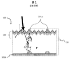
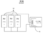
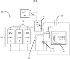
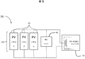
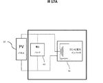
式1中、VPは、太陽パネル10の電圧出力であり、kは構成でのk番目のパネルである。印加外部電圧VAPPと式1の最小/最大印加電圧との関係が維持される限り、スイッチ55は、太陽パネル10にわたり電場250を効率的に印加することができる。
Claims (11)
- 1つ又は複数の光起電デバイスを管理する方法であって、
電圧信号の第1の構成要素を選択された光起電デバイスに印加するステップであって、前記第1の構成要素は、前記選択された光起電デバイスにわたり外部電場を生成するオン状態を表す、第1の構成要素を印加するステップと、
前記電圧信号の第2の構成要素であって、オフサイクルを表す第2の構成要素を前記選択された光起電デバイスに印加するステップと
を含む、方法。 - 前記第1の構成要素を前記選択された光起電デバイスに印加するステップと同時に、前記第1の構成要素を第2の選択された光起電デバイスに印加するステップと、
前記第2の構成要素を前記選択された光起電デバイスに印加するステップと同時に、前記第2の構成要素を前記第2の選択された光起電デバイスに印加するステップと
を更に含む、請求項1に記載の方法。 - 前記第1の構成要素を印加するステップは、高電圧の時変電圧パルスを電圧パルサ回路から印加するステップを含み、前記第2の構成要素を印加するステップは、前記電圧パルサ回路を遮断するステップを含む、請求項1又は2に記載の方法。
- 前記選択された光起電デバイスによって生成された既存の電圧の上に前記第1の構成要素を重ねるステップを更に含み、前記第1の構成要素を重ねるステップは任意選択的に、前記電圧パルサ回路と前記選択された光起電デバイスとの間に結合される上昇注入回路を介して、前記第1の構成要素に負の参照を生成するステップを含む、請求項1〜3の何れか一項に記載の方法。
- 前記第1の構成要素を印加するステップは、電圧源と前記選択された光起電デバイスとの間に配置されるスイッチの第1の位置において、前記電圧源と前記光起電デバイスとを接続するステップを含み、前記第2の構成要素を印加するステップは、前記スイッチの第2の位置において、前記電圧源と前記選択された光起電デバイスとを切断するステップを含む、請求項1〜4の何れか一項に記載の方法。
- 少なくとも1つの光起電デバイスを管理する方法であって、
電圧パルサを選択された光起電デバイスに結合できるようにするステップと、
前記電圧パルサによって生成される電圧信号であって、前記選択された光起電デバイスにわたり外部電場を生成する第1の状態と、オフサイクルを表す第2の状態とを有する電圧信号を前記選択された光起電デバイスに印加するステップと
を含む、方法。 - 上昇注入回路を前記電圧パルサと前記選択された光起電デバイスとの間に結合して、前記第1の状態に負の参照を提供できるようにするステップを更に含む、請求項6に記載の方法。
- 前記電圧信号を第2の選択された光起電デバイスを印加するステップを更に含み、前記電圧信号を任意選択的に前記第2の選択された光起電デバイスに印加するステップは、前記電圧信号を前記選択された光起電デバイスに印加するステップと同時に行われる、請求項6又は7に記載の方法。
- 第2の電圧パルサ回路を前記第2の選択された光起電デバイスに結合して、同時に、前記第1の状態及び前記第2の状態を提供する第2の時変電圧パルスを前記第2の選択された光起電デバイスにわたり提供できるようにするステップを更に含む、請求項8に記載の方法。
- 前記電圧信号を印加するステップは、調整可能な電圧を前記選択された光起電デバイスに印加するステップを含む、請求項6に記載の方法。
- 前記電圧パルサに結合された制御回路を介して、前記第1の状態及び前記第2の状態の周波数及び持続時間のうちの少なくとも一方を制御するステップを更に含む、請求項6に記載の方法。
Applications Claiming Priority (6)
| Application Number | Priority Date | Filing Date | Title |
|---|---|---|---|
| US201461947326P | 2014-03-03 | 2014-03-03 | |
| US61/947,326 | 2014-03-03 | ||
| US201462022087P | 2014-07-08 | 2014-07-08 | |
| US62/022,087 | 2014-07-08 | ||
| US14/628,079 US10069306B2 (en) | 2014-02-21 | 2015-02-20 | System and method for managing the power output of a photovoltaic cell |
| US14/628,079 | 2015-02-20 |
Related Parent Applications (1)
| Application Number | Title | Priority Date | Filing Date |
|---|---|---|---|
| JP2016555354A Division JP6203422B2 (ja) | 2014-03-03 | 2015-03-03 | 電場を複数の太陽パネルに印加する方法及びシステム |
Related Child Applications (1)
| Application Number | Title | Priority Date | Filing Date |
|---|---|---|---|
| JP2018053836A Division JP6578032B2 (ja) | 2014-03-03 | 2018-03-22 | 電場を複数の太陽パネルに印加する方法及びシステム |
Publications (2)
| Publication Number | Publication Date |
|---|---|
| JP2017143731A true JP2017143731A (ja) | 2017-08-17 |
| JP6313494B2 JP6313494B2 (ja) | 2018-04-18 |
Family
ID=54055818
Family Applications (7)
| Application Number | Title | Priority Date | Filing Date |
|---|---|---|---|
| JP2016555354A Expired - Fee Related JP6203422B2 (ja) | 2014-03-03 | 2015-03-03 | 電場を複数の太陽パネルに印加する方法及びシステム |
| JP2017043629A Active JP6313494B2 (ja) | 2014-03-03 | 2017-03-08 | 電場を複数の太陽パネルに印加する方法及びシステム |
| JP2018053836A Expired - Fee Related JP6578032B2 (ja) | 2014-03-03 | 2018-03-22 | 電場を複数の太陽パネルに印加する方法及びシステム |
| JP2019135899A Active JP6838110B2 (ja) | 2014-03-03 | 2019-07-24 | 電場を複数の太陽パネルに印加する方法及びシステム |
| JP2019135898A Active JP6807435B2 (ja) | 2014-03-03 | 2019-07-24 | 電場を複数の太陽パネルに印加する方法及びシステム |
| JP2019135901A Active JP6792675B2 (ja) | 2014-03-03 | 2019-07-24 | 電場を複数の太陽パネルに印加する方法及びシステム |
| JP2020202627A Pending JP2021061748A (ja) | 2014-03-03 | 2020-12-07 | 電場を複数の太陽パネルに印加する方法及びシステム |
Family Applications Before (1)
| Application Number | Title | Priority Date | Filing Date |
|---|---|---|---|
| JP2016555354A Expired - Fee Related JP6203422B2 (ja) | 2014-03-03 | 2015-03-03 | 電場を複数の太陽パネルに印加する方法及びシステム |
Family Applications After (5)
| Application Number | Title | Priority Date | Filing Date |
|---|---|---|---|
| JP2018053836A Expired - Fee Related JP6578032B2 (ja) | 2014-03-03 | 2018-03-22 | 電場を複数の太陽パネルに印加する方法及びシステム |
| JP2019135899A Active JP6838110B2 (ja) | 2014-03-03 | 2019-07-24 | 電場を複数の太陽パネルに印加する方法及びシステム |
| JP2019135898A Active JP6807435B2 (ja) | 2014-03-03 | 2019-07-24 | 電場を複数の太陽パネルに印加する方法及びシステム |
| JP2019135901A Active JP6792675B2 (ja) | 2014-03-03 | 2019-07-24 | 電場を複数の太陽パネルに印加する方法及びシステム |
| JP2020202627A Pending JP2021061748A (ja) | 2014-03-03 | 2020-12-07 | 電場を複数の太陽パネルに印加する方法及びシステム |
Country Status (26)
| Country | Link |
|---|---|
| EP (5) | EP3703217A1 (ja) |
| JP (7) | JP6203422B2 (ja) |
| KR (8) | KR20210110889A (ja) |
| CN (6) | CN106105022B (ja) |
| AP (1) | AP2016009473A0 (ja) |
| AU (7) | AU2015227260B2 (ja) |
| BR (1) | BR112016019755B1 (ja) |
| CA (1) | CA2939004C (ja) |
| CL (3) | CL2016002210A1 (ja) |
| CY (1) | CY1121297T1 (ja) |
| DK (1) | DK3114746T3 (ja) |
| EA (2) | EA037717B1 (ja) |
| ES (4) | ES2665796T3 (ja) |
| HR (1) | HRP20180547T1 (ja) |
| HU (1) | HUE038571T2 (ja) |
| IL (6) | IL266125B (ja) |
| LT (1) | LT3114746T (ja) |
| MX (4) | MX362755B (ja) |
| NZ (1) | NZ722832A (ja) |
| PH (4) | PH12016501643A1 (ja) |
| PL (1) | PL3114746T3 (ja) |
| PT (1) | PT3114746T (ja) |
| RS (1) | RS57174B1 (ja) |
| SG (3) | SG10201912082PA (ja) |
| SI (1) | SI3114746T1 (ja) |
| WO (1) | WO2015134549A1 (ja) |
Cited By (1)
| Publication number | Priority date | Publication date | Assignee | Title |
|---|---|---|---|---|
| CN112820565A (zh) * | 2020-12-29 | 2021-05-18 | 常熟开关制造有限公司(原常熟开关厂) | 自动转换开关电器控制方法及自动转换开关电器 |
Families Citing this family (3)
| Publication number | Priority date | Publication date | Assignee | Title |
|---|---|---|---|---|
| IT201700060644A1 (it) * | 2017-06-01 | 2018-12-01 | Convert Tech S R L | Sistema per energizzare in corrente alternata carichi elettrici in un impianto fotovoltaico |
| RU2732183C1 (ru) * | 2019-12-09 | 2020-09-14 | Валентин Петрович Казанцев | Возобновляемый источник энергии |
| CN116232215B (zh) * | 2023-05-10 | 2023-09-05 | 中国科学院过程工程研究所 | 一种光伏发电装置及方法 |
Citations (1)
| Publication number | Priority date | Publication date | Assignee | Title |
|---|---|---|---|---|
| JPH10173215A (ja) * | 1996-12-16 | 1998-06-26 | Mitsubishi Electric Corp | 太陽電池融雪装置を具備した太陽光発電装置 |
Family Cites Families (31)
| Publication number | Priority date | Publication date | Assignee | Title |
|---|---|---|---|---|
| US5215599A (en) | 1991-05-03 | 1993-06-01 | Electric Power Research Institute | Advanced solar cell |
| JP3206339B2 (ja) * | 1994-11-30 | 2001-09-10 | トヨタ自動車株式会社 | 太陽電池 |
| JPH0936402A (ja) * | 1995-07-21 | 1997-02-07 | Showa Shell Sekiyu Kk | 変換効率向上処理を施した薄膜太陽電池および変換 効率向上手段を付加した薄膜太陽電池アレイ |
| JP3781538B2 (ja) * | 1997-12-17 | 2006-05-31 | シャープ株式会社 | 太陽光発電装置 |
| JPH11233805A (ja) * | 1998-02-13 | 1999-08-27 | Nippon Telegr & Teleph Corp <Ntt> | 光電変換装置 |
| JPH11251615A (ja) * | 1998-03-03 | 1999-09-17 | Canon Inc | 融雪機能付き太陽光発電システム |
| JP4074748B2 (ja) * | 1998-09-03 | 2008-04-09 | マクロニクス インターナショナル カンパニー リミテッド | 浮遊ゲート・メモリ装置にトンネル電流を導入するために調節された電圧源 |
| JP2000323738A (ja) | 1999-05-14 | 2000-11-24 | Kanegafuchi Chem Ind Co Ltd | 太陽電池モジュールの逆バイアス処理装置 |
| AU766466B2 (en) * | 1999-05-14 | 2003-10-16 | Kaneka Corporation | Reverse biasing apparatus for solar battery module |
| AU2001252643A1 (en) * | 2000-08-07 | 2002-02-18 | Norio Akamatsu | Solar ray energy conversion apparatus |
| JP2004079997A (ja) * | 2002-06-19 | 2004-03-11 | Canon Inc | 発電システム及び発電装置 |
| DE102006023563B4 (de) * | 2006-05-19 | 2020-09-10 | Kostal Industrie Elektrik Gmbh | Photovoltaik-Anlage |
| US20090078304A1 (en) * | 2007-09-26 | 2009-03-26 | Jack Arthur Gilmore | Photovoltaic charge abatement device, system, and method |
| CA2737134C (en) * | 2007-10-15 | 2017-10-10 | Ampt, Llc | Systems for highly efficient solar power |
| KR20090128954A (ko) * | 2008-06-12 | 2009-12-16 | 주식회사 엔피홀딩스 | 태양전지 모듈 |
| US7969757B2 (en) * | 2008-12-12 | 2011-06-28 | Array Converter, Inc. | Apparatus providing bias to solar cells |
| EP2249457A1 (en) * | 2009-05-08 | 2010-11-10 | Nxp B.V. | PV solar cell |
| JP2011034942A (ja) | 2009-08-02 | 2011-02-17 | Michio Takaoka | 重畳電界の二次電池と太陽電池 |
| DE102010029813B4 (de) * | 2010-06-08 | 2023-02-23 | Sma Solar Technology Ag | Verfahren zur Steuerung einer elektrischen Stromerzeugung eines Submoduls in einer Photovoltaikanlage |
| US8217258B2 (en) * | 2010-07-09 | 2012-07-10 | Ostendo Technologies, Inc. | Alternating bias hot carrier solar cells |
| KR20120040016A (ko) * | 2010-10-18 | 2012-04-26 | 엘지전자 주식회사 | 태양 전지용 기판 및 태양 전지 |
| JP5912404B2 (ja) * | 2010-10-29 | 2016-04-27 | 株式会社半導体エネルギー研究所 | 光電変換装置 |
| US8466582B2 (en) | 2010-12-03 | 2013-06-18 | Enphase Energy, Inc. | Method and apparatus for applying an electric field to a photovoltaic element |
| KR101449891B1 (ko) * | 2011-05-20 | 2014-10-13 | 솔렉셀, 인크. | 태양 전지를 위한 자가-활성된 전면 바이어스 |
| DE102011115189A1 (de) * | 2011-09-28 | 2013-03-28 | Adensis Gmbh | PV-Anlage mit Sicherung gegen Einspeisung in ein öffentliches Stromversorgungsnetz |
| JP5819172B2 (ja) * | 2011-12-06 | 2015-11-18 | シャープ株式会社 | 電力供給システム |
| US9071191B2 (en) * | 2011-12-28 | 2015-06-30 | John L Patrick | Prefabricated solar array system |
| DE202012011176U1 (de) * | 2012-11-21 | 2013-03-28 | Karl-Heinz Prywerek | Elektrisches Feld als Unterstützung von Photovoltaikanlagen |
| CN103199131B (zh) * | 2013-04-11 | 2016-03-02 | 中国石油大学(华东) | 一种电场增强型肖特基结太阳能电池结构 |
| US10069306B2 (en) * | 2014-02-21 | 2018-09-04 | Solarlytics, Inc. | System and method for managing the power output of a photovoltaic cell |
| US10103547B2 (en) * | 2014-02-21 | 2018-10-16 | Solarlytics, Inc. | Method and system for applying electric fields to multiple solar panels |
-
2015
- 2015-03-03 IL IL266125A patent/IL266125B/en unknown
- 2015-03-03 SG SG10201912082PA patent/SG10201912082PA/en unknown
- 2015-03-03 CN CN201580012041.5A patent/CN106105022B/zh active Active
- 2015-03-03 KR KR1020217027069A patent/KR20210110889A/ko active IP Right Grant
- 2015-03-03 EA EA201891810A patent/EA037717B1/ru unknown
- 2015-03-03 SG SG11201607087SA patent/SG11201607087SA/en unknown
- 2015-03-03 KR KR1020197000365A patent/KR102089916B1/ko active IP Right Grant
- 2015-03-03 RS RS20180404A patent/RS57174B1/sr unknown
- 2015-03-03 DK DK15710361.5T patent/DK3114746T3/en active
- 2015-03-03 WO PCT/US2015/018552 patent/WO2015134549A1/en active Application Filing
- 2015-03-03 ES ES15710361.5T patent/ES2665796T3/es active Active
- 2015-03-03 ES ES17192983T patent/ES2817548T3/es active Active
- 2015-03-03 KR KR1020177005180A patent/KR20170024145A/ko active Application Filing
- 2015-03-03 EP EP20162684.3A patent/EP3703217A1/en active Pending
- 2015-03-03 EP EP15710361.5A patent/EP3114746B1/en active Active
- 2015-03-03 CN CN201710141110.3A patent/CN107039537B/zh active Active
- 2015-03-03 ES ES17192984T patent/ES2811309T3/es active Active
- 2015-03-03 JP JP2016555354A patent/JP6203422B2/ja not_active Expired - Fee Related
- 2015-03-03 SI SI201530218T patent/SI3114746T1/en unknown
- 2015-03-03 HU HUE15710361A patent/HUE038571T2/hu unknown
- 2015-03-03 AP AP2016009473A patent/AP2016009473A0/en unknown
- 2015-03-03 MX MX2016011220A patent/MX362755B/es active IP Right Grant
- 2015-03-03 AU AU2015227260A patent/AU2015227260B2/en not_active Ceased
- 2015-03-03 SG SG10201907499WA patent/SG10201907499WA/en unknown
- 2015-03-03 ES ES16189404T patent/ES2807797T3/es active Active
- 2015-03-03 BR BR112016019755-0A patent/BR112016019755B1/pt not_active IP Right Cessation
- 2015-03-03 NZ NZ722832A patent/NZ722832A/en not_active IP Right Cessation
- 2015-03-03 KR KR1020167027166A patent/KR101778485B1/ko active IP Right Grant
- 2015-03-03 KR KR1020197028209A patent/KR20190112841A/ko not_active IP Right Cessation
- 2015-03-03 KR KR1020197000325A patent/KR102028868B1/ko active IP Right Grant
- 2015-03-03 CA CA2939004A patent/CA2939004C/en active Active
- 2015-03-03 CN CN202011124097.9A patent/CN113300672A/zh active Pending
- 2015-03-03 KR KR1020177033565A patent/KR101978083B1/ko active IP Right Grant
- 2015-03-03 EA EA201691635A patent/EA032397B1/ru not_active IP Right Cessation
- 2015-03-03 PT PT157103615T patent/PT3114746T/pt unknown
- 2015-03-03 EP EP16189404.3A patent/EP3151358B1/en active Active
- 2015-03-03 LT LTEP15710361.5T patent/LT3114746T/lt unknown
- 2015-03-03 CN CN201910053627.6A patent/CN110086420B/zh not_active Expired - Fee Related
- 2015-03-03 CN CN201910053613.4A patent/CN110048671B/zh active Active
- 2015-03-03 CN CN201910053623.8A patent/CN110061693B/zh not_active Expired - Fee Related
- 2015-03-03 EP EP17192983.9A patent/EP3291402B1/en active Active
- 2015-03-03 KR KR1020187007818A patent/KR101937338B1/ko active IP Right Grant
- 2015-03-03 PL PL15710361T patent/PL3114746T3/pl unknown
- 2015-03-03 EP EP17192984.7A patent/EP3291403B8/en active Active
-
2016
- 2016-08-01 IL IL247040A patent/IL247040A0/en unknown
- 2016-08-17 PH PH12016501643A patent/PH12016501643A1/en unknown
- 2016-08-29 MX MX2019000371A patent/MX2019000371A/es unknown
- 2016-08-29 MX MX2019000333A patent/MX2019000333A/es unknown
- 2016-08-29 MX MX2019000379A patent/MX2019000379A/es unknown
- 2016-09-01 CL CL2016002210A patent/CL2016002210A1/es unknown
-
2017
- 2017-03-08 JP JP2017043629A patent/JP6313494B2/ja active Active
- 2017-03-23 PH PH12017500545A patent/PH12017500545B1/en unknown
- 2017-09-21 AU AU2017232123A patent/AU2017232123B2/en not_active Ceased
- 2017-12-21 PH PH12017502394A patent/PH12017502394A1/en unknown
-
2018
- 2018-01-05 PH PH12018500063A patent/PH12018500063A1/en unknown
- 2018-02-13 CL CL2018000393A patent/CL2018000393A1/es unknown
- 2018-03-22 JP JP2018053836A patent/JP6578032B2/ja not_active Expired - Fee Related
- 2018-03-27 CY CY20181100342T patent/CY1121297T1/el unknown
- 2018-04-04 HR HRP20180547TT patent/HRP20180547T1/hr unknown
-
2019
- 2019-04-15 AU AU2019202591A patent/AU2019202591B2/en not_active Ceased
- 2019-04-15 AU AU2019202583A patent/AU2019202583B2/en active Active
- 2019-04-15 AU AU2019202592A patent/AU2019202592B2/en not_active Ceased
- 2019-04-18 AU AU2019202742A patent/AU2019202742B2/en not_active Ceased
- 2019-05-15 IL IL266638A patent/IL266638B/en unknown
- 2019-05-15 IL IL266637A patent/IL266637A/en unknown
- 2019-06-16 IL IL267390A patent/IL267390B/en unknown
- 2019-07-24 JP JP2019135899A patent/JP6838110B2/ja active Active
- 2019-07-24 JP JP2019135898A patent/JP6807435B2/ja active Active
- 2019-07-24 JP JP2019135901A patent/JP6792675B2/ja active Active
- 2019-10-24 CL CL2019003051A patent/CL2019003051A1/es unknown
-
2020
- 2020-12-03 AU AU2020281073A patent/AU2020281073A1/en not_active Abandoned
- 2020-12-07 JP JP2020202627A patent/JP2021061748A/ja active Pending
-
2021
- 2021-09-13 IL IL286371A patent/IL286371A/en unknown
Patent Citations (1)
| Publication number | Priority date | Publication date | Assignee | Title |
|---|---|---|---|---|
| JPH10173215A (ja) * | 1996-12-16 | 1998-06-26 | Mitsubishi Electric Corp | 太陽電池融雪装置を具備した太陽光発電装置 |
Cited By (1)
| Publication number | Priority date | Publication date | Assignee | Title |
|---|---|---|---|---|
| CN112820565A (zh) * | 2020-12-29 | 2021-05-18 | 常熟开关制造有限公司(原常熟开关厂) | 自动转换开关电器控制方法及自动转换开关电器 |
Also Published As
Similar Documents
| Publication | Publication Date | Title |
|---|---|---|
| US11063439B2 (en) | Method and system for applying electric fields to multiple solar panels | |
| JP6578032B2 (ja) | 電場を複数の太陽パネルに印加する方法及びシステム | |
| OA19948A (en) | Method and system for applying electric fields to multiple solar panels. |
Legal Events
| Date | Code | Title | Description |
|---|---|---|---|
| A131 | Notification of reasons for refusal |
Free format text: JAPANESE INTERMEDIATE CODE: A131 Effective date: 20170919 |
|
| A521 | Request for written amendment filed |
Free format text: JAPANESE INTERMEDIATE CODE: A523 Effective date: 20171219 |
|
| A521 | Request for written amendment filed |
Free format text: JAPANESE INTERMEDIATE CODE: A523 Effective date: 20180122 |
|
| TRDD | Decision of grant or rejection written | ||
| A01 | Written decision to grant a patent or to grant a registration (utility model) |
Free format text: JAPANESE INTERMEDIATE CODE: A01 Effective date: 20180220 |
|
| A61 | First payment of annual fees (during grant procedure) |
Free format text: JAPANESE INTERMEDIATE CODE: A61 Effective date: 20180322 |
|
| R150 | Certificate of patent or registration of utility model |
Ref document number: 6313494 Country of ref document: JP Free format text: JAPANESE INTERMEDIATE CODE: R150 |
|
| R250 | Receipt of annual fees |
Free format text: JAPANESE INTERMEDIATE CODE: R250 |
|
| R250 | Receipt of annual fees |
Free format text: JAPANESE INTERMEDIATE CODE: R250 |
|
| R250 | Receipt of annual fees |
Free format text: JAPANESE INTERMEDIATE CODE: R250 |
|
| R250 | Receipt of annual fees |
Free format text: JAPANESE INTERMEDIATE CODE: R250 |