EP3285399B1 - Sensor and heater for stimulus-initiated self-destructing substrate - Google Patents
Sensor and heater for stimulus-initiated self-destructing substrate Download PDFInfo
- Publication number
- EP3285399B1 EP3285399B1 EP17182800.7A EP17182800A EP3285399B1 EP 3285399 B1 EP3285399 B1 EP 3285399B1 EP 17182800 A EP17182800 A EP 17182800A EP 3285399 B1 EP3285399 B1 EP 3285399B1
- Authority
- EP
- European Patent Office
- Prior art keywords
- substrate
- heater
- stressed
- photodiode
- self
- Prior art date
- Legal status (The legal status is an assumption and is not a legal conclusion. Google has not performed a legal analysis and makes no representation as to the accuracy of the status listed.)
- Not-in-force
Links
Images


Classifications
-
- H—ELECTRICITY
- H10—SEMICONDUCTOR DEVICES; ELECTRIC SOLID-STATE DEVICES NOT OTHERWISE PROVIDED FOR
- H10W—GENERIC PACKAGES, INTERCONNECTIONS, CONNECTORS OR OTHER CONSTRUCTIONAL DETAILS OF DEVICES COVERED BY CLASS H10
- H10W42/00—Arrangements for protection of devices
- H10W42/40—Arrangements for protection of devices protecting against tampering, e.g. unauthorised inspection or reverse engineering
- H10W42/405—Arrangements for protection of devices protecting against tampering, e.g. unauthorised inspection or reverse engineering using active circuits
-
- H—ELECTRICITY
- H03—ELECTRONIC CIRCUITRY
- H03K—PULSE TECHNIQUE
- H03K19/00—Logic circuits, i.e. having at least two inputs acting on one output; Inverting circuits
- H03K19/02—Logic circuits, i.e. having at least two inputs acting on one output; Inverting circuits using specified components
- H03K19/173—Logic circuits, i.e. having at least two inputs acting on one output; Inverting circuits using specified components using elementary logic circuits as components
- H03K19/177—Logic circuits, i.e. having at least two inputs acting on one output; Inverting circuits using specified components using elementary logic circuits as components arranged in matrix form
- H03K19/17748—Structural details of configuration resources
- H03K19/17768—Structural details of configuration resources for security
-
- H—ELECTRICITY
- H10—SEMICONDUCTOR DEVICES; ELECTRIC SOLID-STATE DEVICES NOT OTHERWISE PROVIDED FOR
- H10F—INORGANIC SEMICONDUCTOR DEVICES SENSITIVE TO INFRARED RADIATION, LIGHT, ELECTROMAGNETIC RADIATION OF SHORTER WAVELENGTH OR CORPUSCULAR RADIATION
- H10F71/00—Manufacture or treatment of devices covered by this subclass
- H10F71/10—Manufacture or treatment of devices covered by this subclass the devices comprising amorphous semiconductor material
- H10F71/103—Manufacture or treatment of devices covered by this subclass the devices comprising amorphous semiconductor material including only Group IV materials
-
- H—ELECTRICITY
- H10—SEMICONDUCTOR DEVICES; ELECTRIC SOLID-STATE DEVICES NOT OTHERWISE PROVIDED FOR
- H10W—GENERIC PACKAGES, INTERCONNECTIONS, CONNECTORS OR OTHER CONSTRUCTIONAL DETAILS OF DEVICES COVERED BY CLASS H10
- H10W20/00—Interconnections in chips, wafers or substrates
- H10W20/40—Interconnections external to wafers or substrates, e.g. back-end-of-line [BEOL] metallisations or vias connecting to gate electrodes
- H10W20/49—Adaptable interconnections, e.g. fuses or antifuses
- H10W20/493—Fuses, i.e. interconnections changeable from conductive to non-conductive
-
- H—ELECTRICITY
- H10—SEMICONDUCTOR DEVICES; ELECTRIC SOLID-STATE DEVICES NOT OTHERWISE PROVIDED FOR
- H10W—GENERIC PACKAGES, INTERCONNECTIONS, CONNECTORS OR OTHER CONSTRUCTIONAL DETAILS OF DEVICES COVERED BY CLASS H10
- H10W40/00—Arrangements for thermal protection or thermal control
- H10W40/10—Arrangements for heating
-
- H—ELECTRICITY
- H10—SEMICONDUCTOR DEVICES; ELECTRIC SOLID-STATE DEVICES NOT OTHERWISE PROVIDED FOR
- H10W—GENERIC PACKAGES, INTERCONNECTIONS, CONNECTORS OR OTHER CONSTRUCTIONAL DETAILS OF DEVICES COVERED BY CLASS H10
- H10W42/00—Arrangements for protection of devices
- H10W42/40—Arrangements for protection of devices protecting against tampering, e.g. unauthorised inspection or reverse engineering
-
- H—ELECTRICITY
- H10—SEMICONDUCTOR DEVICES; ELECTRIC SOLID-STATE DEVICES NOT OTHERWISE PROVIDED FOR
- H10W—GENERIC PACKAGES, INTERCONNECTIONS, CONNECTORS OR OTHER CONSTRUCTIONAL DETAILS OF DEVICES COVERED BY CLASS H10
- H10W44/00—Electrical arrangements for controlling or matching impedance
-
- H—ELECTRICITY
- H10—SEMICONDUCTOR DEVICES; ELECTRIC SOLID-STATE DEVICES NOT OTHERWISE PROVIDED FOR
- H10W—GENERIC PACKAGES, INTERCONNECTIONS, CONNECTORS OR OTHER CONSTRUCTIONAL DETAILS OF DEVICES COVERED BY CLASS H10
- H10W70/00—Package substrates; Interposers; Redistribution layers [RDL]
- H10W70/60—Insulating or insulated package substrates; Interposers; Redistribution layers
- H10W70/67—Insulating or insulated package substrates; Interposers; Redistribution layers characterised by their insulating layers or insulating parts
- H10W70/69—Insulating materials thereof
- H10W70/692—Ceramics or glasses
-
- H—ELECTRICITY
- H10—SEMICONDUCTOR DEVICES; ELECTRIC SOLID-STATE DEVICES NOT OTHERWISE PROVIDED FOR
- H10D—INORGANIC ELECTRIC SEMICONDUCTOR DEVICES
- H10D18/00—Thyristors
-
- H—ELECTRICITY
- H10—SEMICONDUCTOR DEVICES; ELECTRIC SOLID-STATE DEVICES NOT OTHERWISE PROVIDED FOR
- H10F—INORGANIC SEMICONDUCTOR DEVICES SENSITIVE TO INFRARED RADIATION, LIGHT, ELECTROMAGNETIC RADIATION OF SHORTER WAVELENGTH OR CORPUSCULAR RADIATION
- H10F77/00—Constructional details of devices covered by this subclass
- H10F77/20—Electrodes
- H10F77/206—Electrodes for devices having potential barriers
-
- H—ELECTRICITY
- H10—SEMICONDUCTOR DEVICES; ELECTRIC SOLID-STATE DEVICES NOT OTHERWISE PROVIDED FOR
- H10F—INORGANIC SEMICONDUCTOR DEVICES SENSITIVE TO INFRARED RADIATION, LIGHT, ELECTROMAGNETIC RADIATION OF SHORTER WAVELENGTH OR CORPUSCULAR RADIATION
- H10F77/00—Constructional details of devices covered by this subclass
- H10F77/20—Electrodes
- H10F77/244—Electrodes made of transparent conductive layers, e.g. transparent conductive oxide [TCO] layers
- H10F77/247—Electrodes made of transparent conductive layers, e.g. transparent conductive oxide [TCO] layers comprising indium tin oxide [ITO]
Definitions
- This disclosure relates generally to devices comprising self-destructing substrates and to related methods and systems.
- Some embodiments are directed to a self-destructing device that includes a stressed substrate with a heater thermally coupled to the stressed substrate, the heater comprising a fuse portion.
- the device includes a power source and trigger circuitry.
- the trigger circuitry comprises a sensor and a switch configured to couple the power source to the heater when activated by the trigger signal, wherein, when coupled to the power source for a predetermined period of time, the fuse portion is configured to heat up and break, and wherein, after the fuse portion breaks, the stressed substrate is configured to initiate self-destruction and break during a cool-down cycle.
- a method includes generating a trigger signal in response to exposure to a trigger stimulus.
- a power source is coupled to a heater in response to the trigger signal.
- a stressed substrate is heated after the power source is coupled to the heater, damaging the stressed substrate sufficiently to initiate self-destruction of the stressed substrate, wherein the heater comprises a fuse portion.
- the method further includes heating the fuse portion and the stressed substrate after being coupled to the power source for a predetermined period of time.
- the method further includes breaking the fuse portion and after the fuse portion breaks, initiating self-destruction and breaking the stressed substrate during a cool-down cycle.
- Embodiments disclosed herein relate to electronic devices capable of self destructing by fracturing into small pieces in a controlled, triggerable manner.
- Devices and methods disclosed herein are useful in a variety of applications such as government security and supply chain integrity.
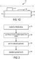
- FIGS. 1A, 1B , and 1C show three versions of a self-destructing device 101, 102, 103 configured to self-destruct in response to a trigger stimulus.
- Self destructing device 101, 102, 103 includes a stressed substrate 110 with a resistive heater 120.
- the heater 120 is thermally coupled to the stressed substrate 110.
- the heater is a resistive conductive film that is energized by flowing electrical current.
- the heater is energized by radio-frequency-coupled microwave.
- the heater is an optical absorber energized by an intense laser beam.
- the heater can be a thin film fuse that breaks when the temperature reaches a sufficiently high value.
- Trigger circuitry 130 is configured to cause the heater 120 to be coupled to a power source 140 in response to exposure to a trigger stimulus.
- the trigger circuitry 130 comprises a sensor 131 and a switch 132.
- the sensor 131 generates a trigger signal when exposed to the trigger stimulus.
- the switch 132 electrically couples the power source 140 to the heater 120.
- the heater 120 When energized by the power source 140, the heater 120 generates heat sufficient to initiate self-destruction of the stressed substrate 110.
- the stressed substrate 110 is engineered to self-destruct by fracturing into many pieces.
- the fracture dynamics are designed so that the substrate 110 self destructs by powderizing, where the fractured pieces are small particles such that most particles have length, width, and height dimensions of less than about 900 ⁇ m, less than about 500 ⁇ m, or even less than about 100 ⁇ m.
- the sensor 131 and switch 132 are located on the stressed substrate 110.
- the switch 132 is not located on the stressed substrate 110.
- neither the sensor 131 nor switch 132 is located on the stressed substrate 110.
- one or more components 150 e.g., electronic components, may be located on the stressed substrate 110 such that when the stressed substrate 110 self-destructs, the components 150 are also destroyed.
- the one or more components 150 may comprise an integrated circuit that generates or stores a cryptographic key. When the integrated circuit is destroyed it renders a processor or other system components inaccessible or non-functional.
- the process used in preparing the stressed substrate 110 e.g., chemical tempering, imparts a large stress gradient within the thickness of the support substrate 110. This stored mechanical energy is abruptly released when a localized area near the heater is heated and damaged. The resulting shock wave causes the substrate 110 to fracture.
- the stressed substrate 110 may be a wafer-like structure including at least one tensile stress layer 115 having a residual tensile stress and at least one compressive stress layer 116 having a residual compressive stress.
- Tensile stress layer 115 and compressive stress layer 116 (collectively referred to herein as "stress-engineered layers”) can be operably integrally connected together such that residual tensile and compressive stresses are self-equilibrating and produce a stress gradient.
- the stress-engineered layers 116 and 115 may be fabricated either by post-treating a substrate material using strategies similar to glass tempering (e.g., by way of heat or chemical treatment), or by depositing the substrate layers using, for example chemical, vapor deposition techniques in which the deposition parameters (i.e., temperature, pressure, chemistry) are varied such that the layers collectively contain a significant inbuilt stress gradient.
- the arrangement of stress-engineered layers 116 and 115 indicated in FIG. 1D is not intended to be limiting in that one or more stressed and/or non-stressed substrate layers may be disposed on and/or between the two stress-engineered layers.
- FIG. 2 is a flow diagram illustrating a method of using the self-destructing device 101, 102, 103 shown in FIGS. 1A through 1D .
- a trigger signal is generated 210 by the sensor in response to exposure of the sensor to the trigger stimulus.
- the trigger signal is a control signal that activates the switch to couple 220 the power source to the heater.
- the heater heats 230 the stressed substrate in a localized area near the heater. The heated area is damaged, which then initiates a rapid release of stored mechanical energy via substrate fracture 240.
- a subsequent cooling after the heating stage initiates propagating fractures in the stressed substrate that causes the stressed substrate to self destruct by breaking apart into many pieces.
- Various methods may be used to generate the stressed substrate 110.
- One example approach involves thin film sputter deposition.
- thin film sputter deposition generally two distinct regimes can be identified leading to very different film morphology and characteristics, and result in either compressive or tensile stress.
- Metals are often used because of functionality (e.g., electrical properties), their structural qualities (e.g., ductility), and the fact that a conductive sputter target allows for a simple, high yield, glow discharge DC magnetron sputtering process.
- stress-engineered metal oxides and glasses can be sputtered as well; these insulating or semiconducting films can be sputter deposited by either radiofrequency (RF) sputtering or by reactive sputtering in a mixed inert/reactive gas plasma (e.g. argon/oxygen).
- RF radiofrequency
- a mixed inert/reactive gas plasma e.g. argon/oxygen
- a method for generating stressed support substrates involves adapting stress-engineered thin film fabrication techniques with ion-exchange tempering to create stress profiles in glass (SiO2) substrates, e.g., glass (SiO2) substrates.
- FIGS. 3A to 3E illustrate a first methodology in which a stressed support substrate 310A is built up by patterned SiO 2 stressed support substrates generated entirely using plasma vapor deposition (PVD) techniques.
- PVD plasma vapor deposition
- This method provides a high degree of control over the specific stress profile generated in the stressed support substrate and provides for continuous control over glass formulation and morphology through the thickness dimension of the stressed support substrate.
- a wafer 300 e.g., silicon or other material
- a release layer 310 most likely a metal.
- a thick liftoff mask 320 is then patterned on release layer 310 such that mask 320 defines an opening 322. Note that wafer 300, release layer 310, and mask 320 form a sacrificial structure. Referring to FIGS.
- PVD processing is then used to create the stress engineered layers 310A-1 and 310A-2 in opening 322, placing stresses in the deposited substrate material 330-1 and 330-2, for example, by altering the process parameters (e.g., using different temperatures T1 and T2 and/or pressures PI and P2).
- the mask is then lifted off, and stressed substrate 310A is singulated (removed) from the remaining sacrificial structure by under-etching the release layer.
- FIGS. 4A to 4E illustrate a second methodology in which a stressed support substrate 410B is built up by patterned SiO 2 on a thin glass core using PVD techniques.
- This methodology provides a high degree of control over the specific stress profile generated in the stressed support substrate.
- the process begins using a substantially unstressed glass core substrate 410B-0 having a thickness T0 in the range of 25 ⁇ m and 100 ⁇ m. Suitable glass core substrates are currently produced by Schott North America, Inc. of Elmsford, New York, USA).
- SiO 2 is then deposited on alternating sides of core substrate 410B-0 via PVD using methods similar to those described above. Specifically, FIG.
- FIG. 4B shows the deposition of material 430-1 in a manner that forms stress-engineered layer 410B-11 on core substrate 41 0B-0.
- FIG. 4C shows the deposition of material 430-2 in a manner that forms stress-engineered layer 410B-21 on an opposite side of core substrate 410B-0.
- FIG. 4C shows the subsequent deposition of material 430-1 in a manner that forms stress-engineered layer 410B-12 on core layer 410B-11
- FIG. 4E shows the deposition of material 430-2 in a manner that forms stress-engineered layer 410B-22 layer 410B-21.
- FIG. 4E shows completed stressed support substrate 410B including core substrate (central, substantially unstressed layer) 410B-0 with stress-engineered layers 410B-11, 410B-12, 410B-21 and 410B-22 formed thereon.
- FIGS. 5A to 5E illustrate a third methodology in which a stressed substrate 510C is produced by subjecting a core substrate to one of an ion-exchange tempering treatment, a chemical treatment and a thermal treatment.
- FIGS. 5A to 5E illustrate an exemplary ion-exchange tempering treatment during which various stress profiles are introduced in a core substrate via molten-salt ion exchange.
- FIG. 5A shows a core substrate 510C-0 over a vat 550 containing a molten-salt solution 555.
- FIG. 5B shows core substrate 510C-0 immediately after submersion in molten-salt solution 2555, FIG.
- FIG. 5C shows core substrate 510C-0 after a first time period of submersion in molten-salt solution 555 in which a first stress-engineered layer 510C-1 is formed
- FIG. 5D shows the structure after a second time period of submersion in molten-salt solution 555 in which a second stress-engineered layer 510C-2 is formed on first stress-engineered layer 510C-1
- FIG. 5E shows completed stressed support substrate 500C including central core substrate 510C-0 and stress-engineered layers 510C-1 and 510C-2.
- a hybrid of the above second and third methods is employed in which diced, thin glass core substrates are ion-exchange tempered, and then multiple layers of SiO2 are deposited on the tempered substrates to further increase the induced stresses.
- the senor 131 may be configured to sense to a variety of trigger stimuli, such as electromagnetic radiation (e.g., radio frequency (RF) radiation, infrared (IR radiation), visible light, ultraviolet (UV) radiation, x-ray radiation, etc.), vibration, a chemical, vapor, gas, sound, temperature, time, moisture, an environmental condition, etc.
- electromagnetic radiation e.g., radio frequency (RF) radiation, infrared (IR radiation), visible light, ultraviolet (UV) radiation, x-ray radiation, etc.
- RF radio frequency
- IR radiation infrared
- UV radiation ultraviolet
- x-ray radiation ultraviolet
- the sensor may be configured to generate the trigger signal in response to exposure to broadband light, such as sunlight or room light, or narrow band light, such as green, red, or blue visible light.
- the green, red or blue light may be produced by a laser.
- the senor 131 is configured to detect a tampering event.
- the tampering event can be detected when the device is exposed to a chemical used for removal of a package cover, the device is vibrated above a threshold vibration, and/or snooping with x-rays that occurs.
- the senor 131 senses time from a clock. When a timer goes off, an electrical current or voltage trigger signal is generated to trigger the switch.
- the senor 131 is a photodiode, e.g., a pn junction diode or p-i-n diode and the trigger signal is a photocurrent generated by the photodiode in response to visible light or other electromagnetic radiation.
- FIG. 6A is a cross sectional view and FIG. 6B is a top view of a p-i-n photodiode sensor 600 that may be used as the sensor 131 of the self destructing device 101, 102, 103 shown in FIGS. 1A through 1D in accordance with some embodiments.
- the photodiode 600 comprises a first electrode layer 620 disposed over the stressed substrate 610.
- the first electrode layer 620 extends over the substrate 610 to form a first lead 133 of the photodiode 600.
- a first doped layer 630 e.g., an n-doped amorphous silicon layer is disposed over the first electrode layer 620.
- An intrinsic layer 640 e.g., an undoped amorphous silicon layer, is disposed between the first doped layer 630 and an oppositely doped second doped layer 650, e.g., a p-doped amorphous silicon layer.
- the first doped layer 630, intrinsic layer 640, and second doped layer 650 form the active region 670 of the p-i-n diode 600.
- a second electrode layer 660 is disposed over the second doped layer 650.
- the second electrode layer 660 substantially transmits the stimulus light that turns on the photodiode 600.
- the second electrode layer 660 may have an optical transmittance greater than 50% at wavelengths of the stimulus light.
- Suitable materials for the second electrode layer 660 include conductive oxides such as indium tin oxide (ITO), conductive polymers, metal grids, carbon nanotubes (CNT), graphene, wire meshes, thin metal films and/or other conductors that have the requisite optical transmittance.
- the device 600 may include an optical filter that narrows the band of wavelengths of light that reach the active region.
- the second electrode layer e.g., ITO layer
- having a suitable thickness provides an optical filter that substantially attenuates wavelengths of light that are outside a wavelength band of the desired trigger stimulus and substantially passes wavelengths of light that are within the wavelength band of the desired trigger stimulus.
- the second electrode layer 660, second doped layer 650, and intrinsic layer 640 extend over the substrate 610 and form a second lead 134 of the photodiode 600.
- the n-doped layer comprises n-doped amorphous silicon (a-Si)
- the p-doped layer comprises p-doped a-Si
- the intrinsic layer comprises intrinsic a-Si.
- FIG. 6 illustrates a p-i-n diode, however, it will be appreciated that in some embodiments a photodiode may be formed by a pn junction without the intrinsic layer.
- the intrinsic layer 640 of the p-i-n photodetector is a 600 nm-thick intrinsic a-Si deposited by plasma-enhanced chemical vapor deposition (PECVD).
- PECVD plasma-enhanced chemical vapor deposition
- the n-layer 630 is a 120 nm-thick phosphorous-doped a-Si deposited by PECVD
- the p-layer 650 is a 20 nm-thick boron-doped a-Si deposited by PECVD.
- This top-side p-layer 650 is designed to be very thin in order to minimize optical absorption of the light being detected.
- the n-electrode 620 is a 200 nm-thick MoCr alloy deposited by sputtering, and the p-electrode 660 is a 55 nm-thick indium-tin-oxide (ITO) designed with an optical thickness optimal for transmitting the wavelength of light being detected.
- ITO indium-tin-oxide
- the first 133 and second 132 leads electrically connect the active region of the photodiode 600 to a periphery of the device as depicted in FIG. 1B .
- the leads 133, 134 may be configured to be connected to external wires 136 that communicate with one or more externally located electronic devices, e.g., the power source 140 and switch 132, which are not disposed on the substrate 110.
- the first electrode layer 620 (first lead 133) and the heater 120 are made of the same materials.
- An adhesion promoting surface 615 such as a barrier layer, may optionally be disposed between the substrate 610 and the first electrode layer 620 and or intrinsic layer 640 of the photodiode 600 and/or the heater.
- the barrier layer comprises a 300 nm-thick PECVD deposited SiO2 barrier layer that enhances film adhesion to the ion-rich surface of the stress-engineered substrate.
- the intrinsic layer 640 (intrinsic a-Si) shown in FIG. 6A may not stick well to the stress-engineered substrate 610, and in that scenario the film stack would crack if the barrier layer 615 is not deposited on the stressed substrate before the intrinsic layer is deposited.
- the ion exchanged stress engineered glass substrate may cause bubbling at the interface between the glass 610 and the photodetector layers 620, 640.
- Suitable materials for the barrier layer 615 include one or more of silicon dioxide (SiO2), silicon nitride (SiN), and silicon oxynitride (SiON).
- the barrier layer 615 may have a thickness greater than 300 nm, greater than 500 nm or between 200 and 700 nm, for example.
- the heater 120 shown in FIGS. 1A and 1B may comprise a fuse portion configured to break at a predetermined temperature.
- FIG. 7A shows a top view of a heater 720 and photodiode 600 disposed on stressed substrate 710 in accordance with some embodiments.
- FIG. 7B shows a cross section taken through line B - B' of the heater 720, photodiode 600, and photodiode leads 133, 134.
- the heater 720 includes a fuse portion 721 and heater leads 722 which are coupled to the ends of the fuse portion 721.
- the fuse portion 721 is a resistive film that operates as a fuse.
- the fuse portion 721 is designed to break (fuse) when heated to a predetermined temperature which occurs after the heater 720 has been connected to the power source for a predetermined period of time.
- the thin film heater 720 can be fabricated out of a variety of materials. Possible materials include MoCr, Cu, and Mg. Once the heater 720 is activated, the fuse portion 721 increases in temperature until the heater material breaks (fuses). The substrate 710 then breaks apart during the cool-down cycle after the heater fuses. The film thickness of the heater 720 must be thick enough for the heater 720 to withstand the delivered electrical power for a sufficient period of time before fusing. If the heater fuses prematurely, the temperature will not rise adequately to trigger the self-destruct process. Hence, consideration should be given to the choice of heater material, impedance value, and film thickness.
- the lateral cross sectional area of the fuse portion 721 taken along line C - C', the length of the fuse portion 721 along line B -B' and/or the material used for the fuse portion contribute to the resistance of the fuse portion 721.
- one or more of the lateral cross sectional area, the length, and/or material of the fuse portion 721 are selected so that a desired, e.g., maximum, power is delivered to the fuse portion 721 by the power source.
- the maximum power may be delivered to the fuse portion 721 when the impedance of the fuse portion 721 is substantially equal to the internal resistance of the power source. Impedance matching ensures efficient transfer of electrical power to the heater 720 when the trigger circuitry switch is activated.
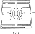
- FIG. 8 is a photograph of a test structure that includes an integrated photodiode 800 and two test heaters 821, 822 which have different lateral cross sectional areas disposed on a stressed substrate 810.
- the heater comprises Mg, MoCr, or Cu.
- the heater is a 2.8 ⁇ m-thick Mg film patterned into a 3 mm long x 500 ⁇ m wide strip.
- MoCr as the heater material
- the heater can be fabricated at the same time as the n-contact electrode of the photodiode, saving one masking and one deposition step.
- a film thickness of about 1.7 ⁇ m produces very similar impedance and fusing characteristics as Mg heaters.
- the desired trigger signal is light from a low power conventional hand-held laser pointer typically used for making presentations. Typical wavelengths are either 532 nm (green) or 650 nm (red).
- the self-destruct sequence is activated by aiming the laser pointer on the photodetector 600 from a distant location.
- the photodetector 600 may be designed to have a large dynamic response, so it causes the electronic switch to trigger reliably when the self-destruct light trigger stimulus is detected, but not when exposed to normal ambient light. This performance feature is achieved by choosing an appropriate combination of layer thicknesses and active region area.
- the photodetector can have active area size of 3 mm x 3 mm in combination with the i and p a-Si layer thickness choices tabulated in Table 1 which provides an exemplary layer structure of an integrated thin film photodetectors sensor at the active region disposed on an ion exchanged glass stressed substrate.
- FIG. 9 shows the photocurrent response when the 3 mm x 3 mm photodetector is in the dark, exposed to ambient light in a bright fluorescent-lit room, illuminated with a bright cell phone LED flashlight at close proximity, and when illuminated with a typical 5 mW green laser pointer.
- the contrast in photocurrent response between ambient light and trigger light exceeds 2 orders of magnitude, so the device architecture disclosed herein allows a wide design margin for choosing a threshold photocurrent that determines when the self-destruct switch is triggered.
- the self destruct switch can be designed to trigger to connect the power source to the heater when the photocurrent is about twice the expected maximum photocurrent produced by the ambient environment of the sensor.
- the photodetector is fabricated so the electrodes/leads are formed together with the active layers in a self aligned fashion, allowing the complete device, including electrical routing leads that connect the active region to the periphery of the substrate, to be made with not more than two masking layers.
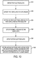
- FIG. 10 is a flow diagram that illustrates a process of making the photodetector.
- FIGS. 11A, 11B , and 6B diagrammatically depict top views that illustrate the process of making the photodetector.
- the photodetector may be formed by first depositing an optional barrier layer on a stress-engineered substrate. A first electrode layer is then deposited 1010 on the barrier layer. In some embodiments, the first electrode layer comprises a MoCr alloy that is sputtered on the barrier layer. A first doped semiconductor layer is deposited 1020 on the first electrode layer. The first doped layer may be an n-doped a-Si layer deposited by PECVD, for example.
- the first doped semiconductor layer and the underlying first electrode layer are then patterned 1030 to form the first electrode region, e.g., by photolithographic patterning of the first electrode layer/first doped layer stack through a first masking step followed by CF4 plasma etching of the first doped layer and chemical wet etching of the first electrode layer.
- FIG. 11A shows a top view of the first electrode region 1101 comprising the first electrode/first doped semiconductor layer stack after the first patterning step.
- An intrinsic layer e.g., intrinsic a-Si and a second, oppositely doped layer, e.g., p-doped a-Si, are deposited 1040 above the patterned first electrode region, e.g. by PECVD.
- the second electrode layer is deposited 1050 above the second doped layer.
- the second electrode layer may comprise ITO deposited by sputtering.
- the second electrode layer is patterned 1060, e.g., by photolithographic exposure through a second mask followed by chemical etching with HCl acid according to the pattern 1102 in FIG. 11B .
- the intrinsic and second doped layers are etched, e.g., with CF4 plasma, also using the second mask.
- This second patterning step not only patterns the second doped and intrinsic layers in the active region, but also selectively removes the remaining portions of the first doped layer above the first electrode layer in the first electrode region formed in the previous patterning step.
- the end result is the device 600 shown in FIGS. 6A and 6B , where the electrodes can be formed together with the active region in a self-aligned manner in only two masking steps.
- the first electrode layer and the heater can be formed simultaneously from the same materials.
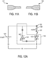
- FIG. 12A provides a circuit schematic for a self-destructing device that includes a photodetector sensor 1231 according to embodiments disclosed herein.
- the trigger circuitry 1230 is configured to activate the switch 1232 at a photocurrent from the sensor 1231 of about 60 ⁇ A, which is midway between the ambient light and laser-illuminated values indicated in the graph of FIG. 9 .
- This choice allows the photodetector 1231 to be exposed to a wide range of ambient light conditions without triggering the self destruct sequence, while ensuring reliable triggering when illuminated with laser pointers having a wide range of laser output power levels.
- the photocurrent from the photodetector 1231 closes the electronic switch 1232, coupling the first terminal 1221 of the thin film heater 1220 integrated on the stress engineered substrate to the power supply 1240.
- the first terminal 1221 is coupled to the power supply 1240 through the switch 1232 electrical current flows in a circuit from the positive terminal of the power source 1240, through terminal 1222, through the heater 1220, through terminal 1221, through the switch 1232, and through the negative terminal of the power source 1240.
- the electrical power delivered to the heater 1220 causes a rapid increase in temperature of the heater, which damages the substrate at that location. The damage causes the substrate to release built-in mechanical stress and to self-destruct into small pieces.
- the p-i-n photodetector 1231 and the heater 1220 may be integrated on the self-destructing substrate, and the electronic switch 1232 is a silicon-controlled rectifier (SCR) located externally from the substrate.
- the SCR may be an off-the-shelf thyristor with part number ST TS110-7 that has a trigger current of close to 60 ⁇ A.
- the SCR switch can be integrated on the self-destructing substrate, as indicated by FIG. 1B .
- Thyristors are suitable switches in some embodiments because the connection latches and remains switched on once triggered, even when the trigger stimulus is subsequently removed. Once triggered, the sensor can become damaged or non-functional without affecting the self-destruction sequence.
- FIG. 12B provides a circuit schematic for a self-destructing device that includes a sensor comprising an RF activated switch 1233 according to embodiments disclosed herein.
- the current through the RF activated switch 1233 closes the electronic switch 1232, coupling the first terminal 1221 of the thin film heater 1220 integrated on the stress engineered substrate to the power supply 1240.
- the switch 1232 electrical current flows in a circuit from the positive terminal of the power source 1240, through terminal 1222, through the heater 1220, through terminal 1221, through the switch 1232, and through the negative terminal of the power source 1240.
- the electrical power delivered to the heater 1220 causes a rapid increase in temperature of the heater, which damages the substrate at that location.
- the RF activated switch 1233 and the electronic switch 1232 may be located externally from the substrate as indicated in FIG. 1C .
- the RF activated switch 1233 and/or the electronic SCR switch can be integrated on the self-destructing substrate, as indicated by FIGS. 1A and/or 1B.
- FIGS. 13 and 14 illustrate in detail the operation of the trigger circuitry in accordance with some embodiments.
- Figure 13 shows an illustration of electrical test probes placed on various locations of the circuit to monitor the self-destruct process.
- FIG. 14 shows the corresponding oscilloscope signals (CH 1, CH 2, CH 3) at various times during the self-destruct process.
- Channel 1 of the oscilloscope (CH 1) measures the voltage between the positive terminal of the power source (V batt ) and the connection between the heater and switch (V SCR ).
- Channel 2 of the oscilloscope (CH 2) represents the measured current through the heater and switch as a voltage.
- Channel 3 of the oscilloscope (CH 3) measures the voltage across the SCR between V SCR and V gate .
- the changes in voltage in the signal traces indicate the progression of the self-destruct process, from the armed state (circuit ready), to the triggered state (electronic switch closed), to the fused state (heater burn-out), and to substrate fracture (substrate self-destructs).
- the time for the heater to fuse is 134 msec from trigger, and the time for the substrate to fracture is 173 msec after trigger.
- the monitoring technique shown in FIGS. 13 and 14 is useful for developing and selecting the choices of thin film materials and processing parameters, and for characterizing their overall effect on the self-destruct sequence.
- FIGS. 15A through 15D show a series of photographs from when a photodetector 1521 is illuminated with a laser pointer to after the substrate 1510 self-destructs.
- FIG. 15A shows the substrate 1510 in a protective enclosure 1505 and a laser pointer 1501 in the foreground.
- FIG. 15B shows the photodetector 1531 being illuminated with light from the laser pointer.
- FIG. 15C shows the substrate 1510 undergoing self-destruction
- FIG. 15D shows the shattered substrate pieces 1502 at the bottom of the enclosure 1505.
- FIGS. 16A through 16D show a series of photographs from before an RF activated switch (not shown) is activated by a keyfob RF transmitter 1601 to after the substrate 1610 self-destructs.
- FIG. 16A shows the substrate 1610 in a protective enclosure 1605 and the RF transmitter 1601 in the foreground.
- FIG. 16B shows the RF transmitter 1601 being activated and a bright spot where the heater 1620 is in the process of fusing.
- FIG. 16C shows the heater 1620 after it has fused.
- FIG. 16D is a photograph taken after self-destruction of the substrate 1610.
Landscapes
- Engineering & Computer Science (AREA)
- Mathematical Physics (AREA)
- Physics & Mathematics (AREA)
- General Engineering & Computer Science (AREA)
- Computer Hardware Design (AREA)
- Computing Systems (AREA)
- Computer Security & Cryptography (AREA)
- Chemical & Material Sciences (AREA)
- Ceramic Engineering (AREA)
- Light Receiving Elements (AREA)
- Semiconductor Integrated Circuits (AREA)
- Logic Circuits (AREA)
- Electric Connection Of Electric Components To Printed Circuits (AREA)
- Photometry And Measurement Of Optical Pulse Characteristics (AREA)
Applications Claiming Priority (1)
| Application Number | Priority Date | Filing Date | Title |
|---|---|---|---|
| US15/220,221 US10224297B2 (en) | 2016-07-26 | 2016-07-26 | Sensor and heater for stimulus-initiated fracture of a substrate |
Publications (3)
| Publication Number | Publication Date |
|---|---|
| EP3285399A2 EP3285399A2 (en) | 2018-02-21 |
| EP3285399A3 EP3285399A3 (en) | 2018-07-25 |
| EP3285399B1 true EP3285399B1 (en) | 2021-09-08 |
Family
ID=59592816
Family Applications (1)
| Application Number | Title | Priority Date | Filing Date |
|---|---|---|---|
| EP17182800.7A Not-in-force EP3285399B1 (en) | 2016-07-26 | 2017-07-24 | Sensor and heater for stimulus-initiated self-destructing substrate |
Country Status (3)
| Country | Link |
|---|---|
| US (2) | US10224297B2 (https=) |
| EP (1) | EP3285399B1 (https=) |
| JP (1) | JP6938257B2 (https=) |
Families Citing this family (16)
| Publication number | Priority date | Publication date | Assignee | Title |
|---|---|---|---|---|
| US9154138B2 (en) | 2013-10-11 | 2015-10-06 | Palo Alto Research Center Incorporated | Stressed substrates for transient electronic systems |
| US9780044B2 (en) | 2015-04-23 | 2017-10-03 | Palo Alto Research Center Incorporated | Transient electronic device with ion-exchanged glass treated interposer |
| US10012250B2 (en) | 2016-04-06 | 2018-07-03 | Palo Alto Research Center Incorporated | Stress-engineered frangible structures |
| US9853001B1 (en) | 2016-06-28 | 2017-12-26 | International Business Machines Corporation | Prevention of reverse engineering of security chips |
| US10224297B2 (en) | 2016-07-26 | 2019-03-05 | Palo Alto Research Center Incorporated | Sensor and heater for stimulus-initiated fracture of a substrate |
| US10026579B2 (en) | 2016-07-26 | 2018-07-17 | Palo Alto Research Center Incorporated | Self-limiting electrical triggering for initiating fracture of frangible glass |
| US10903173B2 (en) | 2016-10-20 | 2021-01-26 | Palo Alto Research Center Incorporated | Pre-conditioned substrate |
| US10626048B2 (en) | 2017-12-18 | 2020-04-21 | Palo Alto Research Center Incorporated | Dissolvable sealant for masking glass in high temperature ion exchange baths |
| US10717669B2 (en) | 2018-05-16 | 2020-07-21 | Palo Alto Research Center Incorporated | Apparatus and method for creating crack initiation sites in a self-fracturing frangible member |
| US11107645B2 (en) | 2018-11-29 | 2021-08-31 | Palo Alto Research Center Incorporated | Functionality change based on stress-engineered components |
| US10947150B2 (en) | 2018-12-03 | 2021-03-16 | Palo Alto Research Center Incorporated | Decoy security based on stress-engineered substrates |
| US10969205B2 (en) | 2019-05-03 | 2021-04-06 | Palo Alto Research Center Incorporated | Electrically-activated pressure vessels for fracturing frangible structures |
| EP4066276A4 (en) * | 2019-11-27 | 2024-03-27 | Corning Incorporated | GLASS WAFER TO MAKE SEMICONDUCTOR DEVICES |
| US12013043B2 (en) * | 2020-12-21 | 2024-06-18 | Xerox Corporation | Triggerable mechanisms and fragment containment arrangements for self-destructing frangible structures and sealed vessels |
| US11904986B2 (en) | 2020-12-21 | 2024-02-20 | Xerox Corporation | Mechanical triggers and triggering methods for self-destructing frangible structures and sealed vessels |
| US11901304B2 (en) * | 2021-05-18 | 2024-02-13 | Globalfoundries U.S. Inc. | Integrated circuit structure with fluorescent material, and related methods |
Family Cites Families (89)
| Publication number | Priority date | Publication date | Assignee | Title |
|---|---|---|---|---|
| US2529210A (en) | 1947-05-23 | 1950-11-07 | Joseph F Butler | Cutting apparatus for wallboards and the like |
| GB1138401A (en) | 1965-05-06 | 1969-01-01 | Mallory & Co Inc P R | Bonding |
| US3601114A (en) | 1969-01-21 | 1971-08-24 | Norton Co | Method and apparatus for cutting complex shapes |
| US3673667A (en) | 1970-11-23 | 1972-07-04 | Whittaker Corp | Method for producing complex shapes by filled billet extrusion |
| US3666967A (en) | 1971-05-12 | 1972-05-30 | Us Navy | Self-destruct aluminum-tungstic oxide films |
| US3882323A (en) * | 1973-12-17 | 1975-05-06 | Us Navy | Method and apparatus for protecting sensitive information contained in thin-film microelectonic circuitry |
| US4102664A (en) | 1977-05-18 | 1978-07-25 | Corning Glass Works | Method for making glass articles with defect-free surfaces |
| US4139359A (en) | 1977-11-02 | 1979-02-13 | Ppg Industries, Inc. | Method and apparatus for shaping glass sheets by roll forming |
| DE3230554C2 (de) | 1982-04-28 | 1984-07-26 | GTI Glastechnische Industrie Peter Lisec, GmbH, Amstetten | Verfahren und Vorrichtung zum Schneiden von Verbundglas |
| SE435352B (sv) | 1983-05-04 | 1984-09-24 | Hydro Betong Ab | Konstruktionskropp for en berande konstruktion bestaende av ett antal med varandra sammanfogade skivor av plastmaterial, av exv uretanskum samt sett att tillverka sagda kropp |
| GB8322258D0 (en) | 1983-08-18 | 1983-09-21 | Holmes A | Security and protection screens |
| US4739555A (en) | 1985-06-18 | 1988-04-26 | Werner Jurgens | Laminated glass cutter |
| FR2681472B1 (fr) | 1991-09-18 | 1993-10-29 | Commissariat Energie Atomique | Procede de fabrication de films minces de materiau semiconducteur. |
| GB9201863D0 (en) | 1992-01-29 | 1992-03-18 | Dunn Kenneth R | Multi glazing air cushion release unit |
| US5791056A (en) | 1996-11-22 | 1998-08-11 | Messina; Gary D. | Emergency glass breaking tool |
| DE19958750B4 (de) | 1999-12-07 | 2006-08-24 | Robert Bosch Gmbh | Leckwellenantenne |
| KR100771258B1 (ko) * | 2000-05-09 | 2007-10-29 | 가부시키가이샤 한도오따이 에네루기 켄큐쇼 | 본인 인증 시스템과 본인 인증 방법 및 휴대 전화 장치 |
| US6418628B1 (en) | 2001-03-22 | 2002-07-16 | Task Force Tips, Inc. | Spring-loaded car window breaker and retractable safety sheath |
| FR2823599B1 (fr) | 2001-04-13 | 2004-12-17 | Commissariat Energie Atomique | Substrat demomtable a tenue mecanique controlee et procede de realisation |
| GB0127083D0 (en) | 2001-11-10 | 2002-01-02 | P W Allen & Company Ltd | Device for breaking glass |
| US20040031966A1 (en) | 2002-08-16 | 2004-02-19 | Forrest Stephen R. | Organic photonic integrated circuit using a photodetector and a transparent organic light emitting device |
| JP2004075504A (ja) | 2002-08-22 | 2004-03-11 | Nippon Sheet Glass Co Ltd | 板ガラスの複曲成形方法及びその装置 |
| DE10305733B4 (de) | 2003-02-12 | 2005-10-20 | Saint Gobain Sekurit D Gmbh | Verfahren zum Erzeugen von Sollbruchstellen in Glasscheiben, Glasscheibe mit Schwächungszone und Verwendung derselben |
| JP4115859B2 (ja) | 2003-02-28 | 2008-07-09 | 株式会社日立製作所 | 陽極接合方法および電子装置 |
| DE10309826B4 (de) | 2003-03-05 | 2009-11-12 | Schott Ag | Verfahren zum Strukturieren von Phosphatgläsern durch zerstörungsfreien Ionenaustausch, strukturierte Phosphatgläser und deren Verwendung |
| US7002517B2 (en) | 2003-06-20 | 2006-02-21 | Anritsu Company | Fixed-frequency beam-steerable leaky-wave microstrip antenna |
| EP1517073A1 (en) | 2003-09-19 | 2005-03-23 | Universita degli Studi di Trento | ESP glass rupture disk |
| EP1671375A4 (en) | 2003-10-09 | 2009-11-25 | Ocas Corp | BOLOMETRIC INFRARED SENSOR WITH TWO-LAYER STRUCTURE AND METHOD OF MANUFACTURING THEREOF |
| US20050082331A1 (en) | 2003-10-17 | 2005-04-21 | Chi-Hong Yang | Tempered glass breaker |
| DE102004015546B4 (de) | 2004-03-30 | 2011-05-12 | Infineon Technologies Ag | Halbleiterchip mit integrierter Schaltung und Verfahren zum Sichern einer integrierten Halbleiterschaltung |
| US20060270190A1 (en) | 2005-05-25 | 2006-11-30 | The Regents Of The University Of California | Method of transferring a thin crystalline semiconductor layer |
| WO2007019277A2 (en) | 2005-08-03 | 2007-02-15 | California Institute Of Technology | Method of forming semiconductor layers on handle substrates |
| US7880248B1 (en) | 2005-10-17 | 2011-02-01 | Teledyne Technologies Incorporated | Destructor integrated circuit chip, interposer electronic device and methods |
| KR101389808B1 (ko) * | 2005-11-18 | 2014-04-29 | 가부시키가이샤 한도오따이 에네루기 켄큐쇼 | 광전변환장치 |
| US8168050B2 (en) * | 2006-07-05 | 2012-05-01 | Momentive Performance Materials Inc. | Electrode pattern for resistance heating element and wafer processing apparatus |
| JP2008216848A (ja) * | 2007-03-07 | 2008-09-18 | Epson Imaging Devices Corp | アレイ基板及び液晶装置、並びに電子機器 |
| GB0717489D0 (en) | 2007-09-08 | 2007-10-17 | Design Factor Ni The Ltd | A Glass breaking device |
| US7623560B2 (en) | 2007-09-27 | 2009-11-24 | Ostendo Technologies, Inc. | Quantum photonic imagers and methods of fabrication thereof |
| JP2009212315A (ja) | 2008-03-04 | 2009-09-17 | Elpida Memory Inc | 半導体装置及びその製造方法 |
| WO2009150558A1 (en) | 2008-06-13 | 2009-12-17 | Nxp B.V. | Intrusion protection using stress changes |
| JP5670901B2 (ja) | 2008-08-08 | 2015-02-18 | コーニング インコーポレイテッド | 強化ガラス物品およびその製造方法 |
| KR20100063269A (ko) | 2008-12-03 | 2010-06-11 | 주식회사 동부하이텍 | 이미지센서 및 그 제조방법 |
| US8089285B2 (en) * | 2009-03-03 | 2012-01-03 | International Business Machines Corporation | Implementing tamper resistant integrated circuit chips |
| US8130072B2 (en) | 2009-05-14 | 2012-03-06 | Palo Alto Research Center Incorporated | Vanadium oxide thermal microprobes |
| CN201532635U (zh) * | 2009-09-03 | 2010-07-21 | 百富计算机技术(深圳)有限公司 | 一种安全保护装置 |
| US8946590B2 (en) | 2009-11-30 | 2015-02-03 | Corning Incorporated | Methods for laser scribing and separating glass substrates |
| FR2953213B1 (fr) | 2009-12-01 | 2013-03-29 | Saint Gobain | Procede de structuration de surface par abrasion ionique,surface structuree et utilisations |
| TWI438162B (zh) | 2010-01-27 | 2014-05-21 | Wintek Corp | 強化玻璃切割方法及強化玻璃切割預置結構 |
| US8393175B2 (en) | 2010-08-26 | 2013-03-12 | Corning Incorporated | Methods for extracting strengthened glass substrates from glass sheets |
| JP6014041B2 (ja) | 2010-10-15 | 2016-10-25 | シーレイト リミテッド ライアビリティー カンパニーSearete Llc | 表面散乱アンテナ |
| US8607590B2 (en) | 2010-11-30 | 2013-12-17 | Corning Incorporated | Methods for separating glass articles from strengthened glass substrate sheets |
| US8616024B2 (en) | 2010-11-30 | 2013-12-31 | Corning Incorporated | Methods for forming grooves and separating strengthened glass substrate sheets |
| US8539794B2 (en) | 2011-02-01 | 2013-09-24 | Corning Incorporated | Strengthened glass substrate sheets and methods for fabricating glass panels from glass substrate sheets |
| WO2012135950A1 (en) | 2011-04-07 | 2012-10-11 | Polyvalor, Limited Partnership | Full-space scanning end-switched crlh leaky-wave antenna |
| US8635887B2 (en) | 2011-08-10 | 2014-01-28 | Corning Incorporated | Methods for separating glass substrate sheets by laser-formed grooves |
| TWI415809B (zh) | 2011-08-12 | 2013-11-21 | Wintek Corp | 強化玻璃單元及其製作方法以及具有強化玻璃單元的覆蓋板 |
| US20130082383A1 (en) | 2011-10-03 | 2013-04-04 | Texas Instruments Incorporated | Electronic assembly having mixed interface including tsv die |
| CN108389893A (zh) | 2011-12-01 | 2018-08-10 | 伊利诺伊大学评议会 | 经设计以经历可编程转变的瞬态器件 |
| CN102617022B (zh) | 2012-03-31 | 2014-10-22 | 洛阳兰迪玻璃机器股份有限公司 | 柱状曲面钢化玻璃加工方法 |
| CN102617023B (zh) | 2012-03-31 | 2014-12-31 | 洛阳兰迪玻璃机器股份有限公司 | 柱状曲面钢化玻璃加工装置 |
| SE537874C2 (sv) | 2012-04-13 | 2015-11-03 | Silex Microsystems Ab | CTE-anpassad interposer och metod att tillverka en sådan |
| US20130273717A1 (en) | 2012-04-17 | 2013-10-17 | Taiwan Semiconductor Manufacturing Co., Ltd. | Apparatus and Method for the Singulation of a Semiconductor Wafer |
| US9938180B2 (en) | 2012-06-05 | 2018-04-10 | Corning Incorporated | Methods of cutting glass using a laser |
| KR101395054B1 (ko) | 2012-08-08 | 2014-05-14 | 삼성코닝정밀소재 주식회사 | 강화유리 커팅 방법 및 강화유리 커팅용 스테이지 |
| US8765536B2 (en) | 2012-09-28 | 2014-07-01 | International Business Machines Corporation | Stress engineered multi-layers for integration of CMOS and Si nanophotonics |
| US8816717B2 (en) | 2012-10-17 | 2014-08-26 | International Business Machines Corporation | Reactive material for integrated circuit tamper detection and response |
| US9385435B2 (en) | 2013-03-15 | 2016-07-05 | The Invention Science Fund I, Llc | Surface scattering antenna improvements |
| WO2014169170A1 (en) | 2013-04-12 | 2014-10-16 | The Board Of Trustees Of The University Of Illinois | Inorganic and organic transient electronic devices |
| US9041205B2 (en) | 2013-06-28 | 2015-05-26 | Intel Corporation | Reliable microstrip routing for electronics components |
| JP5582232B1 (ja) | 2013-07-30 | 2014-09-03 | 日本電気硝子株式会社 | 曲面形状を有するガラス板の製造方法、曲面形状を有するガラス板及び曲面形状を有するガラス板の製造装置 |
| US9790128B2 (en) | 2013-08-07 | 2017-10-17 | Corning Incorporated | Laser controlled ion exchange process and glass articles formed therefrom |
| US9154138B2 (en) * | 2013-10-11 | 2015-10-06 | Palo Alto Research Center Incorporated | Stressed substrates for transient electronic systems |
| US9356603B2 (en) | 2013-10-11 | 2016-05-31 | Palo Alto Research Center Incorporated | Thermally tempered glass substrate using CTE mismatched layers and paste mixtures for transient electronic systems |
| US9294098B2 (en) | 2013-11-26 | 2016-03-22 | Lawrence Livermore National Security, Llc | System and method for on demand, vanishing, high performance electronic systems |
| US9850160B2 (en) | 2013-12-17 | 2017-12-26 | Corning Incorporated | Laser cutting of display glass compositions |
| US9711852B2 (en) | 2014-06-20 | 2017-07-18 | The Invention Science Fund I Llc | Modulation patterns for surface scattering antennas |
| US9853361B2 (en) | 2014-05-02 | 2017-12-26 | The Invention Science Fund I Llc | Surface scattering antennas with lumped elements |
| US10381326B2 (en) | 2014-05-28 | 2019-08-13 | Invensas Corporation | Structure and method for integrated circuits packaging with increased density |
| FR3024136B1 (fr) | 2014-07-24 | 2021-04-30 | Saint Gobain | Procede de rompage d'une feuille de verre |
| US9586857B2 (en) | 2014-11-17 | 2017-03-07 | International Business Machines Corporation | Controlling fragmentation of chemically strengthened glass |
| US9780044B2 (en) | 2015-04-23 | 2017-10-03 | Palo Alto Research Center Incorporated | Transient electronic device with ion-exchanged glass treated interposer |
| US9577047B2 (en) | 2015-07-10 | 2017-02-21 | Palo Alto Research Center Incorporated | Integration of semiconductor epilayers on non-native substrates |
| US10012250B2 (en) | 2016-04-06 | 2018-07-03 | Palo Alto Research Center Incorporated | Stress-engineered frangible structures |
| US10026579B2 (en) | 2016-07-26 | 2018-07-17 | Palo Alto Research Center Incorporated | Self-limiting electrical triggering for initiating fracture of frangible glass |
| US10224297B2 (en) | 2016-07-26 | 2019-03-05 | Palo Alto Research Center Incorporated | Sensor and heater for stimulus-initiated fracture of a substrate |
| US10903173B2 (en) | 2016-10-20 | 2021-01-26 | Palo Alto Research Center Incorporated | Pre-conditioned substrate |
| US10026651B1 (en) | 2017-06-21 | 2018-07-17 | Palo Alto Research Center Incorporated | Singulation of ion-exchanged substrates |
| US10479300B2 (en) | 2017-10-06 | 2019-11-19 | Ford Global Technologies, Llc | Monitoring of vehicle window vibrations for voice-command recognition |
| US10717669B2 (en) | 2018-05-16 | 2020-07-21 | Palo Alto Research Center Incorporated | Apparatus and method for creating crack initiation sites in a self-fracturing frangible member |
-
2016
- 2016-07-26 US US15/220,221 patent/US10224297B2/en active Active
-
2017
- 2017-07-20 JP JP2017140416A patent/JP6938257B2/ja not_active Expired - Fee Related
- 2017-07-24 EP EP17182800.7A patent/EP3285399B1/en not_active Not-in-force
-
2019
- 2019-01-25 US US16/257,304 patent/US10903176B2/en active Active
Also Published As
| Publication number | Publication date |
|---|---|
| JP2018018819A (ja) | 2018-02-01 |
| JP6938257B2 (ja) | 2021-09-22 |
| US20180033742A1 (en) | 2018-02-01 |
| US10903176B2 (en) | 2021-01-26 |
| US20190172800A1 (en) | 2019-06-06 |
| US10224297B2 (en) | 2019-03-05 |
| EP3285399A3 (en) | 2018-07-25 |
| EP3285399A2 (en) | 2018-02-21 |
Similar Documents
| Publication | Publication Date | Title |
|---|---|---|
| EP3285399B1 (en) | Sensor and heater for stimulus-initiated self-destructing substrate | |
| US11810871B2 (en) | Pre-conditioned self-destructing substrate | |
| JP6533757B2 (ja) | イオン交換ガラス処理されたインターポーザを伴う過渡的な電子デバイス | |
| US10332717B2 (en) | Self-limiting electrical triggering for initiating fracture of frangible glass | |
| US9154138B2 (en) | Stressed substrates for transient electronic systems | |
| US9294098B2 (en) | System and method for on demand, vanishing, high performance electronic systems | |
| US11459266B2 (en) | Apparatus and method for creating crack initiation sites in a self-fracturing frangible member | |
| CN107210537A (zh) | 多频带波长选择性装置 | |
| CN106098846A (zh) | 一种用于非制冷红外探测器参考像元及其制造方法 | |
| US7915585B2 (en) | Microbolometer pixel and fabrication method utilizing ion implantation | |
| US11107645B2 (en) | Functionality change based on stress-engineered components | |
| CN112786539B (zh) | 一种基于阵列式孔道的二级激发自毁芯片及其制备方法 | |
| CN105579832A (zh) | 红外线放射装置及其制造方法 | |
| JP5672742B2 (ja) | 赤外線温度センサ | |
| JP3033143B2 (ja) | ガスセンサの製造方法 | |
| JP3594923B2 (ja) | サーモパイル式赤外線センサの製造方法 | |
| JP3269200B2 (ja) | 焦電型赤外線検出素子及びその製造方法 | |
| JP3232801B2 (ja) | 焦電型赤外線検出素子の製造方法 | |
| JPH08271341A (ja) | 焦電型赤外線検出素子の製造方法 | |
| CN110160658A (zh) | 一种刻蚀增强型的非制冷红外薄膜探测器及制备方法 | |
| JP2002048822A (ja) | 微弱電流検知手段、及びこれを用いた漏れ電流遮断装置 | |
| JP2013229398A (ja) | 熱電変換素子及びその製造方法 |
Legal Events
| Date | Code | Title | Description |
|---|---|---|---|
| PUAI | Public reference made under article 153(3) epc to a published international application that has entered the european phase |
Free format text: ORIGINAL CODE: 0009012 |
|
| STAA | Information on the status of an ep patent application or granted ep patent |
Free format text: STATUS: THE APPLICATION HAS BEEN PUBLISHED |
|
| AK | Designated contracting states |
Kind code of ref document: A2 Designated state(s): AL AT BE BG CH CY CZ DE DK EE ES FI FR GB GR HR HU IE IS IT LI LT LU LV MC MK MT NL NO PL PT RO RS SE SI SK SM TR |
|
| AX | Request for extension of the european patent |
Extension state: BA ME |
|
| PUAL | Search report despatched |
Free format text: ORIGINAL CODE: 0009013 |
|
| AK | Designated contracting states |
Kind code of ref document: A3 Designated state(s): AL AT BE BG CH CY CZ DE DK EE ES FI FR GB GR HR HU IE IS IT LI LT LU LV MC MK MT NL NO PL PT RO RS SE SI SK SM TR |
|
| AX | Request for extension of the european patent |
Extension state: BA ME |
|
| RIC1 | Information provided on ipc code assigned before grant |
Ipc: H03K 19/177 20060101AFI20180620BHEP Ipc: H01L 23/00 20060101ALI20180620BHEP |
|
| STAA | Information on the status of an ep patent application or granted ep patent |
Free format text: STATUS: REQUEST FOR EXAMINATION WAS MADE |
|
| 17P | Request for examination filed |
Effective date: 20190125 |
|
| RBV | Designated contracting states (corrected) |
Designated state(s): AL AT BE BG CH CY CZ DE DK EE ES FI FR GB GR HR HU IE IS IT LI LT LU LV MC MK MT NL NO PL PT RO RS SE SI SK SM TR |
|
| GRAP | Despatch of communication of intention to grant a patent |
Free format text: ORIGINAL CODE: EPIDOSNIGR1 |
|
| STAA | Information on the status of an ep patent application or granted ep patent |
Free format text: STATUS: GRANT OF PATENT IS INTENDED |
|
| INTG | Intention to grant announced |
Effective date: 20210325 |
|
| RIN1 | Information on inventor provided before grant (corrected) |
Inventor name: WANG, QIAN Inventor name: LUJAN, RENE A. Inventor name: LIMB, SCOTT J. Inventor name: WHITING, GREGORY Inventor name: LU, JENG PING Inventor name: CHUA, CHRISTOPHER L. |
|
| GRAS | Grant fee paid |
Free format text: ORIGINAL CODE: EPIDOSNIGR3 |
|
| GRAA | (expected) grant |
Free format text: ORIGINAL CODE: 0009210 |
|
| STAA | Information on the status of an ep patent application or granted ep patent |
Free format text: STATUS: THE PATENT HAS BEEN GRANTED |
|
| AK | Designated contracting states |
Kind code of ref document: B1 Designated state(s): AL AT BE BG CH CY CZ DE DK EE ES FI FR GB GR HR HU IE IS IT LI LT LU LV MC MK MT NL NO PL PT RO RS SE SI SK SM TR |
|
| REG | Reference to a national code |
Ref country code: GB Ref legal event code: FG4D |
|
| REG | Reference to a national code |
Ref country code: CH Ref legal event code: EP Ref country code: AT Ref legal event code: REF Ref document number: 1429492 Country of ref document: AT Kind code of ref document: T Effective date: 20210915 |
|
| REG | Reference to a national code |
Ref country code: DE Ref legal event code: R096 Ref document number: 602017045574 Country of ref document: DE |
|
| REG | Reference to a national code |
Ref country code: IE Ref legal event code: FG4D |
|
| REG | Reference to a national code |
Ref country code: LT Ref legal event code: MG9D |
|
| REG | Reference to a national code |
Ref country code: NL Ref legal event code: MP Effective date: 20210908 |
|
| PG25 | Lapsed in a contracting state [announced via postgrant information from national office to epo] |
Ref country code: RS Free format text: LAPSE BECAUSE OF FAILURE TO SUBMIT A TRANSLATION OF THE DESCRIPTION OR TO PAY THE FEE WITHIN THE PRESCRIBED TIME-LIMIT Effective date: 20210908 Ref country code: SE Free format text: LAPSE BECAUSE OF FAILURE TO SUBMIT A TRANSLATION OF THE DESCRIPTION OR TO PAY THE FEE WITHIN THE PRESCRIBED TIME-LIMIT Effective date: 20210908 Ref country code: LT Free format text: LAPSE BECAUSE OF FAILURE TO SUBMIT A TRANSLATION OF THE DESCRIPTION OR TO PAY THE FEE WITHIN THE PRESCRIBED TIME-LIMIT Effective date: 20210908 Ref country code: BG Free format text: LAPSE BECAUSE OF FAILURE TO SUBMIT A TRANSLATION OF THE DESCRIPTION OR TO PAY THE FEE WITHIN THE PRESCRIBED TIME-LIMIT Effective date: 20211208 Ref country code: NO Free format text: LAPSE BECAUSE OF FAILURE TO SUBMIT A TRANSLATION OF THE DESCRIPTION OR TO PAY THE FEE WITHIN THE PRESCRIBED TIME-LIMIT Effective date: 20211208 Ref country code: HR Free format text: LAPSE BECAUSE OF FAILURE TO SUBMIT A TRANSLATION OF THE DESCRIPTION OR TO PAY THE FEE WITHIN THE PRESCRIBED TIME-LIMIT Effective date: 20210908 Ref country code: FI Free format text: LAPSE BECAUSE OF FAILURE TO SUBMIT A TRANSLATION OF THE DESCRIPTION OR TO PAY THE FEE WITHIN THE PRESCRIBED TIME-LIMIT Effective date: 20210908 Ref country code: ES Free format text: LAPSE BECAUSE OF FAILURE TO SUBMIT A TRANSLATION OF THE DESCRIPTION OR TO PAY THE FEE WITHIN THE PRESCRIBED TIME-LIMIT Effective date: 20210908 |
|
| REG | Reference to a national code |
Ref country code: AT Ref legal event code: MK05 Ref document number: 1429492 Country of ref document: AT Kind code of ref document: T Effective date: 20210908 |
|
| PG25 | Lapsed in a contracting state [announced via postgrant information from national office to epo] |
Ref country code: LV Free format text: LAPSE BECAUSE OF FAILURE TO SUBMIT A TRANSLATION OF THE DESCRIPTION OR TO PAY THE FEE WITHIN THE PRESCRIBED TIME-LIMIT Effective date: 20210908 Ref country code: GR Free format text: LAPSE BECAUSE OF FAILURE TO SUBMIT A TRANSLATION OF THE DESCRIPTION OR TO PAY THE FEE WITHIN THE PRESCRIBED TIME-LIMIT Effective date: 20211209 |
|
| PG25 | Lapsed in a contracting state [announced via postgrant information from national office to epo] |
Ref country code: AT Free format text: LAPSE BECAUSE OF FAILURE TO SUBMIT A TRANSLATION OF THE DESCRIPTION OR TO PAY THE FEE WITHIN THE PRESCRIBED TIME-LIMIT Effective date: 20210908 |
|
| PG25 | Lapsed in a contracting state [announced via postgrant information from national office to epo] |
Ref country code: IS Free format text: LAPSE BECAUSE OF FAILURE TO SUBMIT A TRANSLATION OF THE DESCRIPTION OR TO PAY THE FEE WITHIN THE PRESCRIBED TIME-LIMIT Effective date: 20220108 Ref country code: SM Free format text: LAPSE BECAUSE OF FAILURE TO SUBMIT A TRANSLATION OF THE DESCRIPTION OR TO PAY THE FEE WITHIN THE PRESCRIBED TIME-LIMIT Effective date: 20210908 Ref country code: SK Free format text: LAPSE BECAUSE OF FAILURE TO SUBMIT A TRANSLATION OF THE DESCRIPTION OR TO PAY THE FEE WITHIN THE PRESCRIBED TIME-LIMIT Effective date: 20210908 Ref country code: RO Free format text: LAPSE BECAUSE OF FAILURE TO SUBMIT A TRANSLATION OF THE DESCRIPTION OR TO PAY THE FEE WITHIN THE PRESCRIBED TIME-LIMIT Effective date: 20210908 Ref country code: PT Free format text: LAPSE BECAUSE OF FAILURE TO SUBMIT A TRANSLATION OF THE DESCRIPTION OR TO PAY THE FEE WITHIN THE PRESCRIBED TIME-LIMIT Effective date: 20220110 Ref country code: PL Free format text: LAPSE BECAUSE OF FAILURE TO SUBMIT A TRANSLATION OF THE DESCRIPTION OR TO PAY THE FEE WITHIN THE PRESCRIBED TIME-LIMIT Effective date: 20210908 Ref country code: NL Free format text: LAPSE BECAUSE OF FAILURE TO SUBMIT A TRANSLATION OF THE DESCRIPTION OR TO PAY THE FEE WITHIN THE PRESCRIBED TIME-LIMIT Effective date: 20210908 Ref country code: EE Free format text: LAPSE BECAUSE OF FAILURE TO SUBMIT A TRANSLATION OF THE DESCRIPTION OR TO PAY THE FEE WITHIN THE PRESCRIBED TIME-LIMIT Effective date: 20210908 Ref country code: CZ Free format text: LAPSE BECAUSE OF FAILURE TO SUBMIT A TRANSLATION OF THE DESCRIPTION OR TO PAY THE FEE WITHIN THE PRESCRIBED TIME-LIMIT Effective date: 20210908 Ref country code: AL Free format text: LAPSE BECAUSE OF FAILURE TO SUBMIT A TRANSLATION OF THE DESCRIPTION OR TO PAY THE FEE WITHIN THE PRESCRIBED TIME-LIMIT Effective date: 20210908 |
|
| REG | Reference to a national code |
Ref country code: DE Ref legal event code: R097 Ref document number: 602017045574 Country of ref document: DE |
|
| PLBE | No opposition filed within time limit |
Free format text: ORIGINAL CODE: 0009261 |
|
| STAA | Information on the status of an ep patent application or granted ep patent |
Free format text: STATUS: NO OPPOSITION FILED WITHIN TIME LIMIT |
|
| PG25 | Lapsed in a contracting state [announced via postgrant information from national office to epo] |
Ref country code: DK Free format text: LAPSE BECAUSE OF FAILURE TO SUBMIT A TRANSLATION OF THE DESCRIPTION OR TO PAY THE FEE WITHIN THE PRESCRIBED TIME-LIMIT Effective date: 20210908 |
|
| 26N | No opposition filed |
Effective date: 20220609 |
|
| PG25 | Lapsed in a contracting state [announced via postgrant information from national office to epo] |
Ref country code: SI Free format text: LAPSE BECAUSE OF FAILURE TO SUBMIT A TRANSLATION OF THE DESCRIPTION OR TO PAY THE FEE WITHIN THE PRESCRIBED TIME-LIMIT Effective date: 20210908 |
|
| PG25 | Lapsed in a contracting state [announced via postgrant information from national office to epo] |
Ref country code: IT Free format text: LAPSE BECAUSE OF FAILURE TO SUBMIT A TRANSLATION OF THE DESCRIPTION OR TO PAY THE FEE WITHIN THE PRESCRIBED TIME-LIMIT Effective date: 20210908 |
|
| PG25 | Lapsed in a contracting state [announced via postgrant information from national office to epo] |
Ref country code: MC Free format text: LAPSE BECAUSE OF FAILURE TO SUBMIT A TRANSLATION OF THE DESCRIPTION OR TO PAY THE FEE WITHIN THE PRESCRIBED TIME-LIMIT Effective date: 20210908 |
|
| REG | Reference to a national code |
Ref country code: CH Ref legal event code: PL |
|
| REG | Reference to a national code |
Ref country code: BE Ref legal event code: MM Effective date: 20220731 |
|
| PG25 | Lapsed in a contracting state [announced via postgrant information from national office to epo] |
Ref country code: LU Free format text: LAPSE BECAUSE OF NON-PAYMENT OF DUE FEES Effective date: 20220724 Ref country code: LI Free format text: LAPSE BECAUSE OF NON-PAYMENT OF DUE FEES Effective date: 20220731 Ref country code: CH Free format text: LAPSE BECAUSE OF NON-PAYMENT OF DUE FEES Effective date: 20220731 |
|
| PG25 | Lapsed in a contracting state [announced via postgrant information from national office to epo] |
Ref country code: BE Free format text: LAPSE BECAUSE OF NON-PAYMENT OF DUE FEES Effective date: 20220731 |
|
| P01 | Opt-out of the competence of the unified patent court (upc) registered |
Effective date: 20230528 |
|
| PG25 | Lapsed in a contracting state [announced via postgrant information from national office to epo] |
Ref country code: IE Free format text: LAPSE BECAUSE OF NON-PAYMENT OF DUE FEES Effective date: 20220724 |
|
| PGFP | Annual fee paid to national office [announced via postgrant information from national office to epo] |
Ref country code: GB Payment date: 20230713 Year of fee payment: 7 |
|
| PGFP | Annual fee paid to national office [announced via postgrant information from national office to epo] |
Ref country code: FR Payment date: 20230710 Year of fee payment: 7 Ref country code: DE Payment date: 20230712 Year of fee payment: 7 |
|
| PG25 | Lapsed in a contracting state [announced via postgrant information from national office to epo] |
Ref country code: HU Free format text: LAPSE BECAUSE OF FAILURE TO SUBMIT A TRANSLATION OF THE DESCRIPTION OR TO PAY THE FEE WITHIN THE PRESCRIBED TIME-LIMIT; INVALID AB INITIO Effective date: 20170724 |
|
| PG25 | Lapsed in a contracting state [announced via postgrant information from national office to epo] |
Ref country code: MK Free format text: LAPSE BECAUSE OF FAILURE TO SUBMIT A TRANSLATION OF THE DESCRIPTION OR TO PAY THE FEE WITHIN THE PRESCRIBED TIME-LIMIT Effective date: 20210908 Ref country code: CY Free format text: LAPSE BECAUSE OF FAILURE TO SUBMIT A TRANSLATION OF THE DESCRIPTION OR TO PAY THE FEE WITHIN THE PRESCRIBED TIME-LIMIT Effective date: 20210908 |
|
| PG25 | Lapsed in a contracting state [announced via postgrant information from national office to epo] |
Ref country code: MT Free format text: LAPSE BECAUSE OF FAILURE TO SUBMIT A TRANSLATION OF THE DESCRIPTION OR TO PAY THE FEE WITHIN THE PRESCRIBED TIME-LIMIT Effective date: 20210908 |
|
| REG | Reference to a national code |
Ref country code: DE Ref legal event code: R119 Ref document number: 602017045574 Country of ref document: DE |
|
| GBPC | Gb: european patent ceased through non-payment of renewal fee |
Effective date: 20240724 |
|
| PG25 | Lapsed in a contracting state [announced via postgrant information from national office to epo] |
Ref country code: DE Free format text: LAPSE BECAUSE OF NON-PAYMENT OF DUE FEES Effective date: 20250201 |
|
| PG25 | Lapsed in a contracting state [announced via postgrant information from national office to epo] |
Ref country code: FR Free format text: LAPSE BECAUSE OF NON-PAYMENT OF DUE FEES Effective date: 20240731 |
|
| PG25 | Lapsed in a contracting state [announced via postgrant information from national office to epo] |
Ref country code: GB Free format text: LAPSE BECAUSE OF NON-PAYMENT OF DUE FEES Effective date: 20240724 |
|
| PG25 | Lapsed in a contracting state [announced via postgrant information from national office to epo] |
Ref country code: TR Free format text: LAPSE BECAUSE OF FAILURE TO SUBMIT A TRANSLATION OF THE DESCRIPTION OR TO PAY THE FEE WITHIN THE PRESCRIBED TIME-LIMIT Effective date: 20210908 |