EP3273491B1 - Optical semiconductor element with light reflecting layer and phosphor layer - Google Patents
Optical semiconductor element with light reflecting layer and phosphor layer Download PDFInfo
- Publication number
- EP3273491B1 EP3273491B1 EP16764849.2A EP16764849A EP3273491B1 EP 3273491 B1 EP3273491 B1 EP 3273491B1 EP 16764849 A EP16764849 A EP 16764849A EP 3273491 B1 EP3273491 B1 EP 3273491B1
- Authority
- EP
- European Patent Office
- Prior art keywords
- light reflecting
- optical semiconductor
- layer
- phosphor
- sheet
- Prior art date
- Legal status (The legal status is an assumption and is not a legal conclusion. Google has not performed a legal analysis and makes no representation as to the accuracy of the status listed.)
- Active
Links
- 239000004065 semiconductor Substances 0.000 title claims description 268
- 230000003287 optical effect Effects 0.000 title claims description 260
- OAICVXFJPJFONN-UHFFFAOYSA-N Phosphorus Chemical compound [P] OAICVXFJPJFONN-UHFFFAOYSA-N 0.000 title claims description 259
- 229920005989 resin Polymers 0.000 claims description 78
- 239000011347 resin Substances 0.000 claims description 78
- 230000002093 peripheral effect Effects 0.000 claims description 52
- 238000002156 mixing Methods 0.000 claims description 5
- 239000000463 material Substances 0.000 claims description 2
- 239000010410 layer Substances 0.000 description 383
- 239000004820 Pressure-sensitive adhesive Substances 0.000 description 92
- 238000011049 filling Methods 0.000 description 80
- 238000000034 method Methods 0.000 description 71
- 238000005520 cutting process Methods 0.000 description 48
- 229920001187 thermosetting polymer Polymers 0.000 description 31
- 239000002904 solvent Substances 0.000 description 28
- 239000000203 mixture Substances 0.000 description 26
- 238000004519 manufacturing process Methods 0.000 description 24
- 238000010438 heat treatment Methods 0.000 description 20
- 239000002245 particle Substances 0.000 description 16
- 238000005498 polishing Methods 0.000 description 15
- 229920002050 silicone resin Polymers 0.000 description 13
- 238000006243 chemical reaction Methods 0.000 description 11
- 238000007731 hot pressing Methods 0.000 description 9
- 238000010030 laminating Methods 0.000 description 7
- 239000011248 coating agent Substances 0.000 description 6
- 238000000576 coating method Methods 0.000 description 6
- 238000007789 sealing Methods 0.000 description 6
- 239000000654 additive Substances 0.000 description 5
- 230000000996 additive effect Effects 0.000 description 5
- 230000000694 effects Effects 0.000 description 5
- 239000004744 fabric Substances 0.000 description 5
- 238000012986 modification Methods 0.000 description 5
- 230000004048 modification Effects 0.000 description 5
- 238000005580 one pot reaction Methods 0.000 description 5
- 239000002966 varnish Substances 0.000 description 5
- 238000002844 melting Methods 0.000 description 4
- 230000008018 melting Effects 0.000 description 4
- 229910052751 metal Inorganic materials 0.000 description 4
- 239000002184 metal Substances 0.000 description 4
- 125000002496 methyl group Chemical group [H]C([H])([H])* 0.000 description 4
- 125000001997 phenyl group Chemical group [H]C1=C([H])C([H])=C(*)C([H])=C1[H] 0.000 description 4
- 239000007779 soft material Substances 0.000 description 4
- ZWEHNKRNPOVVGH-UHFFFAOYSA-N 2-Butanone Chemical compound CCC(C)=O ZWEHNKRNPOVVGH-UHFFFAOYSA-N 0.000 description 3
- LFQSCWFLJHTTHZ-UHFFFAOYSA-N Ethanol Chemical compound CCO LFQSCWFLJHTTHZ-UHFFFAOYSA-N 0.000 description 3
- OKKJLVBELUTLKV-UHFFFAOYSA-N Methanol Chemical compound OC OKKJLVBELUTLKV-UHFFFAOYSA-N 0.000 description 3
- YXFVVABEGXRONW-UHFFFAOYSA-N Toluene Chemical compound CC1=CC=CC=C1 YXFVVABEGXRONW-UHFFFAOYSA-N 0.000 description 3
- 239000007788 liquid Substances 0.000 description 3
- 238000005259 measurement Methods 0.000 description 3
- VLKZOEOYAKHREP-UHFFFAOYSA-N n-Hexane Chemical compound CCCCCC VLKZOEOYAKHREP-UHFFFAOYSA-N 0.000 description 3
- -1 polyethylene Polymers 0.000 description 3
- 238000012545 processing Methods 0.000 description 3
- 239000000758 substrate Substances 0.000 description 3
- 238000007039 two-step reaction Methods 0.000 description 3
- CSCPPACGZOOCGX-UHFFFAOYSA-N Acetone Chemical compound CC(C)=O CSCPPACGZOOCGX-UHFFFAOYSA-N 0.000 description 2
- 239000004925 Acrylic resin Substances 0.000 description 2
- 229920000178 Acrylic resin Polymers 0.000 description 2
- VTYYLEPIZMXCLO-UHFFFAOYSA-L Calcium carbonate Chemical compound [Ca+2].[O-]C([O-])=O VTYYLEPIZMXCLO-UHFFFAOYSA-L 0.000 description 2
- 239000004698 Polyethylene Substances 0.000 description 2
- PPBRXRYQALVLMV-UHFFFAOYSA-N Styrene Chemical compound C=CC1=CC=CC=C1 PPBRXRYQALVLMV-UHFFFAOYSA-N 0.000 description 2
- WYURNTSHIVDZCO-UHFFFAOYSA-N Tetrahydrofuran Chemical compound C1CCOC1 WYURNTSHIVDZCO-UHFFFAOYSA-N 0.000 description 2
- 229910000004 White lead Inorganic materials 0.000 description 2
- XLOMVQKBTHCTTD-UHFFFAOYSA-N Zinc monoxide Chemical compound [Zn]=O XLOMVQKBTHCTTD-UHFFFAOYSA-N 0.000 description 2
- 239000000853 adhesive Substances 0.000 description 2
- 230000001070 adhesive effect Effects 0.000 description 2
- JNDMLEXHDPKVFC-UHFFFAOYSA-N aluminum;oxygen(2-);yttrium(3+) Chemical compound [O-2].[O-2].[O-2].[Al+3].[Y+3] JNDMLEXHDPKVFC-UHFFFAOYSA-N 0.000 description 2
- 150000004945 aromatic hydrocarbons Chemical class 0.000 description 2
- 229910052788 barium Inorganic materials 0.000 description 2
- 239000000919 ceramic Substances 0.000 description 2
- 239000003822 epoxy resin Substances 0.000 description 2
- 239000010954 inorganic particle Substances 0.000 description 2
- 229910052909 inorganic silicate Inorganic materials 0.000 description 2
- 239000011159 matrix material Substances 0.000 description 2
- 230000007246 mechanism Effects 0.000 description 2
- 239000011146 organic particle Substances 0.000 description 2
- 239000003960 organic solvent Substances 0.000 description 2
- 229920000647 polyepoxide Polymers 0.000 description 2
- 229920006267 polyester film Polymers 0.000 description 2
- 229920000573 polyethylene Polymers 0.000 description 2
- 229920001721 polyimide Polymers 0.000 description 2
- 239000009719 polyimide resin Substances 0.000 description 2
- 229920006254 polymer film Polymers 0.000 description 2
- 229920001296 polysiloxane Polymers 0.000 description 2
- 238000004382 potting Methods 0.000 description 2
- 238000003825 pressing Methods 0.000 description 2
- 230000000630 rising effect Effects 0.000 description 2
- 239000007787 solid Substances 0.000 description 2
- 229910052712 strontium Inorganic materials 0.000 description 2
- 238000012546 transfer Methods 0.000 description 2
- XLYOFNOQVPJJNP-UHFFFAOYSA-N water Substances O XLYOFNOQVPJJNP-UHFFFAOYSA-N 0.000 description 2
- 229910019901 yttrium aluminum garnet Inorganic materials 0.000 description 2
- GZVHEAJQGPRDLQ-UHFFFAOYSA-N 6-phenyl-1,3,5-triazine-2,4-diamine Chemical compound NC1=NC(N)=NC(C=2C=CC=CC=2)=N1 GZVHEAJQGPRDLQ-UHFFFAOYSA-N 0.000 description 1
- 239000005995 Aluminium silicate Substances 0.000 description 1
- JOYRKODLDBILNP-UHFFFAOYSA-N Ethyl urethane Chemical compound CCOC(N)=O JOYRKODLDBILNP-UHFFFAOYSA-N 0.000 description 1
- 239000004640 Melamine resin Substances 0.000 description 1
- 229920000877 Melamine resin Polymers 0.000 description 1
- BPQQTUXANYXVAA-UHFFFAOYSA-N Orthosilicate Chemical compound [O-][Si]([O-])([O-])[O-] BPQQTUXANYXVAA-UHFFFAOYSA-N 0.000 description 1
- 229910003564 SiAlON Inorganic materials 0.000 description 1
- GWEVSGVZZGPLCZ-UHFFFAOYSA-N Titan oxide Chemical compound O=[Ti]=O GWEVSGVZZGPLCZ-UHFFFAOYSA-N 0.000 description 1
- 229920001807 Urea-formaldehyde Polymers 0.000 description 1
- NIXOWILDQLNWCW-UHFFFAOYSA-N acrylic acid group Chemical group C(C=C)(=O)O NIXOWILDQLNWCW-UHFFFAOYSA-N 0.000 description 1
- 150000001298 alcohols Chemical class 0.000 description 1
- 150000001338 aliphatic hydrocarbons Chemical class 0.000 description 1
- FNCIDSNKNZQJTJ-UHFFFAOYSA-N alumane;terbium Chemical compound [AlH3].[Tb] FNCIDSNKNZQJTJ-UHFFFAOYSA-N 0.000 description 1
- 235000012211 aluminium silicate Nutrition 0.000 description 1
- 239000003125 aqueous solvent Substances 0.000 description 1
- FZTPSPNAZCIDGO-UHFFFAOYSA-N barium(2+);silicate Chemical compound [Ba+2].[Ba+2].[O-][Si]([O-])([O-])[O-] FZTPSPNAZCIDGO-UHFFFAOYSA-N 0.000 description 1
- 238000005422 blasting Methods 0.000 description 1
- 229910052791 calcium Inorganic materials 0.000 description 1
- 239000011575 calcium Substances 0.000 description 1
- 229910000019 calcium carbonate Inorganic materials 0.000 description 1
- 150000004649 carbonic acid derivatives Chemical class 0.000 description 1
- 239000002734 clay mineral Substances 0.000 description 1
- 229910021438 complex inorganic oxide Inorganic materials 0.000 description 1
- 239000013078 crystal Substances 0.000 description 1
- 230000001419 dependent effect Effects 0.000 description 1
- 238000009826 distribution Methods 0.000 description 1
- 229920001971 elastomer Polymers 0.000 description 1
- 238000005530 etching Methods 0.000 description 1
- 150000002170 ethers Chemical class 0.000 description 1
- 238000000605 extraction Methods 0.000 description 1
- 239000011888 foil Substances 0.000 description 1
- 239000002223 garnet Substances 0.000 description 1
- 238000001879 gelation Methods 0.000 description 1
- 239000011521 glass Substances 0.000 description 1
- NLYAJNPCOHFWQQ-UHFFFAOYSA-N kaolin Chemical compound O.O.O=[Al]O[Si](=O)O[Si](=O)O[Al]=O NLYAJNPCOHFWQQ-UHFFFAOYSA-N 0.000 description 1
- 150000002576 ketones Chemical class 0.000 description 1
- RYZCLUQMCYZBJQ-UHFFFAOYSA-H lead(2+);dicarbonate;dihydroxide Chemical compound [OH-].[OH-].[Pb+2].[Pb+2].[Pb+2].[O-]C([O-])=O.[O-]C([O-])=O RYZCLUQMCYZBJQ-UHFFFAOYSA-H 0.000 description 1
- 238000000465 moulding Methods 0.000 description 1
- 150000004767 nitrides Chemical class 0.000 description 1
- RVTZCBVAJQQJTK-UHFFFAOYSA-N oxygen(2-);zirconium(4+) Chemical compound [O-2].[O-2].[Zr+4] RVTZCBVAJQQJTK-UHFFFAOYSA-N 0.000 description 1
- 239000005011 phenolic resin Substances 0.000 description 1
- 229920002401 polyacrylamide Polymers 0.000 description 1
- 229920006122 polyamide resin Polymers 0.000 description 1
- 229920005668 polycarbonate resin Polymers 0.000 description 1
- 239000004431 polycarbonate resin Substances 0.000 description 1
- 229920001225 polyester resin Polymers 0.000 description 1
- 239000004645 polyester resin Substances 0.000 description 1
- 229920005672 polyolefin resin Polymers 0.000 description 1
- 238000003860 storage Methods 0.000 description 1
- 238000012360 testing method Methods 0.000 description 1
- YLQBMQCUIZJEEH-UHFFFAOYSA-N tetrahydrofuran Natural products C=1C=COC=1 YLQBMQCUIZJEEH-UHFFFAOYSA-N 0.000 description 1
- 229920002803 thermoplastic polyurethane Polymers 0.000 description 1
- 229920005992 thermoplastic resin Polymers 0.000 description 1
- OGIDPMRJRNCKJF-UHFFFAOYSA-N titanium oxide Inorganic materials [Ti]=O OGIDPMRJRNCKJF-UHFFFAOYSA-N 0.000 description 1
- 229920006337 unsaturated polyester resin Polymers 0.000 description 1
- 239000011787 zinc oxide Substances 0.000 description 1
- 229910001928 zirconium oxide Inorganic materials 0.000 description 1
Images


Classifications
-
- H—ELECTRICITY
- H01—ELECTRIC ELEMENTS
- H01L—SEMICONDUCTOR DEVICES NOT COVERED BY CLASS H10
- H01L33/00—Semiconductor devices having potential barriers specially adapted for light emission; Processes or apparatus specially adapted for the manufacture or treatment thereof or of parts thereof; Details thereof
- H01L33/48—Semiconductor devices having potential barriers specially adapted for light emission; Processes or apparatus specially adapted for the manufacture or treatment thereof or of parts thereof; Details thereof characterised by the semiconductor body packages
- H01L33/58—Optical field-shaping elements
- H01L33/60—Reflective elements
-
- H—ELECTRICITY
- H01—ELECTRIC ELEMENTS
- H01L—SEMICONDUCTOR DEVICES NOT COVERED BY CLASS H10
- H01L33/00—Semiconductor devices having potential barriers specially adapted for light emission; Processes or apparatus specially adapted for the manufacture or treatment thereof or of parts thereof; Details thereof
- H01L33/48—Semiconductor devices having potential barriers specially adapted for light emission; Processes or apparatus specially adapted for the manufacture or treatment thereof or of parts thereof; Details thereof characterised by the semiconductor body packages
- H01L33/50—Wavelength conversion elements
-
- H—ELECTRICITY
- H01—ELECTRIC ELEMENTS
- H01L—SEMICONDUCTOR DEVICES NOT COVERED BY CLASS H10
- H01L24/00—Arrangements for connecting or disconnecting semiconductor or solid-state bodies; Methods or apparatus related thereto
- H01L24/93—Batch processes
- H01L24/95—Batch processes at chip-level, i.e. with connecting carried out on a plurality of singulated devices, i.e. on diced chips
- H01L24/97—Batch processes at chip-level, i.e. with connecting carried out on a plurality of singulated devices, i.e. on diced chips the devices being connected to a common substrate, e.g. interposer, said common substrate being separable into individual assemblies after connecting
-
- H—ELECTRICITY
- H01—ELECTRIC ELEMENTS
- H01L—SEMICONDUCTOR DEVICES NOT COVERED BY CLASS H10
- H01L25/00—Assemblies consisting of a plurality of individual semiconductor or other solid state devices ; Multistep manufacturing processes thereof
- H01L25/03—Assemblies consisting of a plurality of individual semiconductor or other solid state devices ; Multistep manufacturing processes thereof all the devices being of a type provided for in the same subgroup of groups H01L27/00 - H01L33/00, or in a single subclass of H10K, H10N, e.g. assemblies of rectifier diodes
- H01L25/04—Assemblies consisting of a plurality of individual semiconductor or other solid state devices ; Multistep manufacturing processes thereof all the devices being of a type provided for in the same subgroup of groups H01L27/00 - H01L33/00, or in a single subclass of H10K, H10N, e.g. assemblies of rectifier diodes the devices not having separate containers
- H01L25/075—Assemblies consisting of a plurality of individual semiconductor or other solid state devices ; Multistep manufacturing processes thereof all the devices being of a type provided for in the same subgroup of groups H01L27/00 - H01L33/00, or in a single subclass of H10K, H10N, e.g. assemblies of rectifier diodes the devices not having separate containers the devices being of a type provided for in group H01L33/00
- H01L25/0753—Assemblies consisting of a plurality of individual semiconductor or other solid state devices ; Multistep manufacturing processes thereof all the devices being of a type provided for in the same subgroup of groups H01L27/00 - H01L33/00, or in a single subclass of H10K, H10N, e.g. assemblies of rectifier diodes the devices not having separate containers the devices being of a type provided for in group H01L33/00 the devices being arranged next to each other
-
- H—ELECTRICITY
- H01—ELECTRIC ELEMENTS
- H01L—SEMICONDUCTOR DEVICES NOT COVERED BY CLASS H10
- H01L33/00—Semiconductor devices having potential barriers specially adapted for light emission; Processes or apparatus specially adapted for the manufacture or treatment thereof or of parts thereof; Details thereof
- H01L33/005—Processes
-
- H—ELECTRICITY
- H01—ELECTRIC ELEMENTS
- H01L—SEMICONDUCTOR DEVICES NOT COVERED BY CLASS H10
- H01L33/00—Semiconductor devices having potential barriers specially adapted for light emission; Processes or apparatus specially adapted for the manufacture or treatment thereof or of parts thereof; Details thereof
- H01L33/02—Semiconductor devices having potential barriers specially adapted for light emission; Processes or apparatus specially adapted for the manufacture or treatment thereof or of parts thereof; Details thereof characterised by the semiconductor bodies
- H01L33/10—Semiconductor devices having potential barriers specially adapted for light emission; Processes or apparatus specially adapted for the manufacture or treatment thereof or of parts thereof; Details thereof characterised by the semiconductor bodies with a light reflecting structure, e.g. semiconductor Bragg reflector
-
- H—ELECTRICITY
- H01—ELECTRIC ELEMENTS
- H01L—SEMICONDUCTOR DEVICES NOT COVERED BY CLASS H10
- H01L33/00—Semiconductor devices having potential barriers specially adapted for light emission; Processes or apparatus specially adapted for the manufacture or treatment thereof or of parts thereof; Details thereof
- H01L33/36—Semiconductor devices having potential barriers specially adapted for light emission; Processes or apparatus specially adapted for the manufacture or treatment thereof or of parts thereof; Details thereof characterised by the electrodes
-
- H—ELECTRICITY
- H01—ELECTRIC ELEMENTS
- H01L—SEMICONDUCTOR DEVICES NOT COVERED BY CLASS H10
- H01L33/00—Semiconductor devices having potential barriers specially adapted for light emission; Processes or apparatus specially adapted for the manufacture or treatment thereof or of parts thereof; Details thereof
- H01L33/44—Semiconductor devices having potential barriers specially adapted for light emission; Processes or apparatus specially adapted for the manufacture or treatment thereof or of parts thereof; Details thereof characterised by the coatings, e.g. passivation layer or anti-reflective coating
- H01L33/46—Reflective coating, e.g. dielectric Bragg reflector
-
- H—ELECTRICITY
- H01—ELECTRIC ELEMENTS
- H01L—SEMICONDUCTOR DEVICES NOT COVERED BY CLASS H10
- H01L33/00—Semiconductor devices having potential barriers specially adapted for light emission; Processes or apparatus specially adapted for the manufacture or treatment thereof or of parts thereof; Details thereof
- H01L33/48—Semiconductor devices having potential barriers specially adapted for light emission; Processes or apparatus specially adapted for the manufacture or treatment thereof or of parts thereof; Details thereof characterised by the semiconductor body packages
- H01L33/50—Wavelength conversion elements
- H01L33/505—Wavelength conversion elements characterised by the shape, e.g. plate or foil
-
- H—ELECTRICITY
- H01—ELECTRIC ELEMENTS
- H01L—SEMICONDUCTOR DEVICES NOT COVERED BY CLASS H10
- H01L2224/00—Indexing scheme for arrangements for connecting or disconnecting semiconductor or solid-state bodies and methods related thereto as covered by H01L24/00
- H01L2224/01—Means for bonding being attached to, or being formed on, the surface to be connected, e.g. chip-to-package, die-attach, "first-level" interconnects; Manufacturing methods related thereto
- H01L2224/10—Bump connectors; Manufacturing methods related thereto
- H01L2224/12—Structure, shape, material or disposition of the bump connectors prior to the connecting process
- H01L2224/12105—Bump connectors formed on an encapsulation of the semiconductor or solid-state body, e.g. bumps on chip-scale packages
-
- H—ELECTRICITY
- H01—ELECTRIC ELEMENTS
- H01L—SEMICONDUCTOR DEVICES NOT COVERED BY CLASS H10
- H01L2224/00—Indexing scheme for arrangements for connecting or disconnecting semiconductor or solid-state bodies and methods related thereto as covered by H01L24/00
- H01L2224/01—Means for bonding being attached to, or being formed on, the surface to be connected, e.g. chip-to-package, die-attach, "first-level" interconnects; Manufacturing methods related thereto
- H01L2224/10—Bump connectors; Manufacturing methods related thereto
- H01L2224/15—Structure, shape, material or disposition of the bump connectors after the connecting process
- H01L2224/16—Structure, shape, material or disposition of the bump connectors after the connecting process of an individual bump connector
- H01L2224/161—Disposition
- H01L2224/16151—Disposition the bump connector connecting between a semiconductor or solid-state body and an item not being a semiconductor or solid-state body, e.g. chip-to-substrate, chip-to-passive
- H01L2224/16221—Disposition the bump connector connecting between a semiconductor or solid-state body and an item not being a semiconductor or solid-state body, e.g. chip-to-substrate, chip-to-passive the body and the item being stacked
- H01L2224/16225—Disposition the bump connector connecting between a semiconductor or solid-state body and an item not being a semiconductor or solid-state body, e.g. chip-to-substrate, chip-to-passive the body and the item being stacked the item being non-metallic, e.g. insulating substrate with or without metallisation
- H01L2224/16227—Disposition the bump connector connecting between a semiconductor or solid-state body and an item not being a semiconductor or solid-state body, e.g. chip-to-substrate, chip-to-passive the body and the item being stacked the item being non-metallic, e.g. insulating substrate with or without metallisation the bump connector connecting to a bond pad of the item
-
- H—ELECTRICITY
- H01—ELECTRIC ELEMENTS
- H01L—SEMICONDUCTOR DEVICES NOT COVERED BY CLASS H10
- H01L2224/00—Indexing scheme for arrangements for connecting or disconnecting semiconductor or solid-state bodies and methods related thereto as covered by H01L24/00
- H01L2224/93—Batch processes
- H01L2224/95—Batch processes at chip-level, i.e. with connecting carried out on a plurality of singulated devices, i.e. on diced chips
- H01L2224/96—Batch processes at chip-level, i.e. with connecting carried out on a plurality of singulated devices, i.e. on diced chips the devices being encapsulated in a common layer, e.g. neo-wafer or pseudo-wafer, said common layer being separable into individual assemblies after connecting
-
- H—ELECTRICITY
- H01—ELECTRIC ELEMENTS
- H01L—SEMICONDUCTOR DEVICES NOT COVERED BY CLASS H10
- H01L2224/00—Indexing scheme for arrangements for connecting or disconnecting semiconductor or solid-state bodies and methods related thereto as covered by H01L24/00
- H01L2224/93—Batch processes
- H01L2224/95—Batch processes at chip-level, i.e. with connecting carried out on a plurality of singulated devices, i.e. on diced chips
- H01L2224/97—Batch processes at chip-level, i.e. with connecting carried out on a plurality of singulated devices, i.e. on diced chips the devices being connected to a common substrate, e.g. interposer, said common substrate being separable into individual assemblies after connecting
-
- H—ELECTRICITY
- H01—ELECTRIC ELEMENTS
- H01L—SEMICONDUCTOR DEVICES NOT COVERED BY CLASS H10
- H01L2924/00—Indexing scheme for arrangements or methods for connecting or disconnecting semiconductor or solid-state bodies as covered by H01L24/00
- H01L2924/10—Details of semiconductor or other solid state devices to be connected
- H01L2924/11—Device type
- H01L2924/12—Passive devices, e.g. 2 terminal devices
- H01L2924/1204—Optical Diode
- H01L2924/12041—LED
-
- H—ELECTRICITY
- H01—ELECTRIC ELEMENTS
- H01L—SEMICONDUCTOR DEVICES NOT COVERED BY CLASS H10
- H01L2924/00—Indexing scheme for arrangements or methods for connecting or disconnecting semiconductor or solid-state bodies as covered by H01L24/00
- H01L2924/10—Details of semiconductor or other solid state devices to be connected
- H01L2924/11—Device type
- H01L2924/12—Passive devices, e.g. 2 terminal devices
- H01L2924/1204—Optical Diode
- H01L2924/12042—LASER
-
- H—ELECTRICITY
- H01—ELECTRIC ELEMENTS
- H01L—SEMICONDUCTOR DEVICES NOT COVERED BY CLASS H10
- H01L2933/00—Details relating to devices covered by the group H01L33/00 but not provided for in its subgroups
- H01L2933/0008—Processes
- H01L2933/0025—Processes relating to coatings
-
- H—ELECTRICITY
- H01—ELECTRIC ELEMENTS
- H01L—SEMICONDUCTOR DEVICES NOT COVERED BY CLASS H10
- H01L2933/00—Details relating to devices covered by the group H01L33/00 but not provided for in its subgroups
- H01L2933/0008—Processes
- H01L2933/0033—Processes relating to semiconductor body packages
- H01L2933/0041—Processes relating to semiconductor body packages relating to wavelength conversion elements
-
- H—ELECTRICITY
- H01—ELECTRIC ELEMENTS
- H01L—SEMICONDUCTOR DEVICES NOT COVERED BY CLASS H10
- H01L2933/00—Details relating to devices covered by the group H01L33/00 but not provided for in its subgroups
- H01L2933/0008—Processes
- H01L2933/0033—Processes relating to semiconductor body packages
- H01L2933/0058—Processes relating to semiconductor body packages relating to optical field-shaping elements
Definitions
- the invention relates to an optical semiconductor element.
- the plurality of light emitting elements are flip-chip mounted on a board at spaced intervals to each other in a surface direction and thereafter, a liquid resin containing light reflective particles is subjected to potting (dropping) between light emitting elements that are next to each other with a dispenser (quantitative liquid discharge device), so that the coating member is disposed on the side surfaces of the plurality of light emitting elements.
- EP 2 680 327 A2 describes a method for producing a reflecting layer-phosphor layer-covered light emitting diode (LED) which includes a disposing step of disposing a reflecting layer at one side in a thickness direction of a support; a reflecting layer covering step of, after the disposing step, disposing an LED having a terminal at one surface thereof at the one side in the thickness direction of the support so as to allow the one surface of the LED to be covered with the reflecting layer; and a phosphor layer covering step of forming a phosphor layer so as to cover at least the other surface of the LED.
- LED reflecting layer-phosphor layer-covered light emitting diode
- US 2012/0319150 A1 relates to a method for manufacturing a semiconductor light emitting device which includes: preparing a metal plate including first frames and second frames, the first frames and the second frames being alternately arranged and spaced from each other, a light emitting element being fixed to each of the first frames, the light emitting element being connected to an adjacent one of the second frames via a metal wire; molding a first resin on the metal plate, the first resin covering the first frame, the second frame, and the light emitting element; forming in the first resin a groove defining a resin package including the first frame, the second frame, and the light emitting element; filling a second resin inside the groove; and forming the resin package with an outer edge of the first resin covered with the second resin by cutting the second resin along the groove.
- WO 2014/091914 A1 describes an LED device which is compact while having good luminous efficiency and a focused light distribution.
- This LED device is provided with: a reflective frame around the outer periphery of the LED device; an LED die which has a transparent insulating substrate, a semiconductor layer formed on the bottom surface of the transparent insulating substrate, and an outer connection electrode disposed on the semiconductor layer; and a fluorescent member which is disposed on at least the top surface of the LED die and which converts the wavelength of the light emitted from the LED die.
- a method of producing a light-emitting device including: preparing a plurality of light-emitting elements each including element electrodes in a pair; arranging the plurality of light-emitting elements in a sealing member to expose at least one surface of each of the element electrodes in a pair provided to each of the light-emitting elements; forming external connection electrodes in a plurality of pairs on the sealing member, the external connection electrodes in each pair being electrically connected to the element electrodes in a pair provided to each of the light-emitting elements; and obtaining a plurality of light-emitting devices by dividing the sealing member with the plurality of light-emitting elements, the light-emitting devices each including a light-emitting element having element electrodes in a pair, a sealing member sealing the light-emitting element while at
- the coating member is attached to the upper surface of the light emitting element. Then, there is a disadvantage that light emitted from the light emitting element upwardly is reflected by the coating member, and thus, light cannot be efficiently taken out to the outside.
- An object of the invention is to provide a method for producing a light reflecting layer-including optical semiconductor element, and a method for producing a light reflecting layer and phosphor layer-including optical semiconductor element having excellent light extraction efficiency.
- the description furthermore includes a number of methods for producing an optical semiconductor device, these methods not forming part of the invention.
- the description includes a first method for producing a light reflecting layer-including optical semiconductor element including the steps of temporarily fixing electrode surfaces of a plurality of optical semiconductor elements each having the electrode surface provided with an electrode, a light emitting surface opposing the electrode surface and provided with a light emitting layer, and a connecting surface connecting a peripheral end edge of the electrode surface to that of the light emitting surface to a temporarily fixing sheet at spaced intervals to each other; filling a first gap between the optical semiconductor elements that are next to each other with a light reflecting sheet and forming a light reflecting layer on the connecting surfaces of the plurality of optical semiconductor elements; removing the light reflecting layer attaching to the light emitting surfaces of the plurality of optical semiconductor elements; and cutting the light reflecting layer between the optical semiconductor elements that are next to each other.
- the light reflecting layer attaching to the light emitting surfaces of the plurality of optical semiconductor elements is removed, so that light that is emitted from the light emitting surfaces of the plurality of optical semiconductor elements can be efficiently taken out.
- the description furthermore includes a modification of the first method for producing a light reflecting layer-including optical semiconductor element described above, wherein the light reflecting sheet has a shape continuing in a direction perpendicular to a thickness direction so as to include the plurality of optical semiconductor elements when projected in the thickness direction of the light reflecting sheet.
- the light reflecting sheet has a shape continuing in the direction perpendicular to the thickness direction so as to include the plurality of optical semiconductor elements when projected in the thickness direction of the light reflecting sheet, so that the light reflecting sheet can easily fill the first gap.
- the description furthermore includes a second method for producing a light reflecting layer and phosphor layer-including optical semiconductor element including the steps of temporarily fixing electrode surfaces of a plurality of optical semiconductor elements each having the electrode surface provided with an electrode, a light emitting surface opposing the electrode surface and provided with a light emitting layer, and a connecting surface connecting a peripheral end edge of the electrode surface to that of the light emitting surface to a temporarily fixing sheet at spaced intervals to each other; forming a phosphor layer on the light emitting surfaces of the plurality of optical semiconductor elements so as to form a second gap between the optical semiconductor elements that are next to each other; filling the second gap with a light reflecting sheet and forming a light reflecting layer on the side surface of the phosphor layer opposing the second gap; removing the light reflecting layer attaching to the surface of the phosphor layer; and cutting the light reflecting layer between the phosphor layers that are next to each other.
- the light reflecting layer attaching to the surface of the phosphor layer is removed, so that light that is emitted from the light emitting surfaces of the plurality of optical semiconductor elements and in which wavelength conversion is performed by the phosphor layer can be efficiently taken out.
- the description furthermore includes a modification of the second method for producing a light reflecting layer and phosphor layer-including optical semiconductor element described above, wherein in the step of forming the phosphor layer, the phosphor layer is also formed on the connecting surfaces of the plurality of optical semiconductor elements.
- the phosphor layer is also formed on the connecting surface of the optical semiconductor element in the light reflecting layer and phosphor layer-including optical semiconductor element, so that the wavelength of light that is emitted from the connecting surface of the optical semiconductor element can be efficiently converted, and thereafter, the light can be surely reflected by the light reflecting layer that is formed on the side surface of the phosphor layer opposing the second gap.
- the description furthermore includes a modification of the second method for producing a light reflecting layer and phosphor layer-including optical semiconductor element described above, wherein the step of forming the phosphor layer includes the steps of filling a first gap between the optical semiconductor elements that are next to each other with a phosphor sheet having a shape continuing in a direction perpendicular to a thickness direction so as to include the plurality of optical semiconductor elements when projected in the thickness direction, and cutting the phosphor layer between the optical semiconductor elements that are next to each other so as to form the second gap.
- the phosphor sheet can easily fill the first gap and next, the second gap can be easily formed.
- the description furthermore includes a modification of the second method for producing a light reflecting layer and phosphor layer-including optical semiconductor element described above, wherein in the step of forming the phosphor layer, the phosphor sheet having a pattern corresponding to the light emitting surfaces of the plurality of optical semiconductor elements when projected in the thickness direction is disposed on the light emitting surfaces of the plurality of optical semiconductor elements, and in the step of forming the light reflecting layer, the light reflecting layer is formed on the connecting surfaces of the plurality of optical semiconductor elements.
- the light reflecting layer is formed on the connecting surfaces of the plurality of optical semiconductor elements, so that light that is emitted from the connecting surface of the optical semiconductor element can be efficiently reflected by the light reflecting layer.
- the description furthermore includes a modification of the second method for producing a light reflecting layer and phosphor layer-including optical semiconductor element described above, wherein the light reflecting sheet has a shape continuing in a direction perpendicular to a thickness direction so as to include the plurality of optical semiconductor elements when projected in the thickness direction of the light reflecting sheet.
- the light reflecting sheet has a shape continuing in the direction perpendicular to the thickness direction so as to include the plurality of optical semiconductor elements when projected in the thickness direction of the light reflecting sheet, so that the light reflecting sheet can easily fill the second gap.
- the light reflecting layer and phosphor layer-including optical semiconductor element of the invention According to the light reflecting layer and phosphor layer-including optical semiconductor element of the invention, light that is emitted from the light emitting surfaces of the plurality of optical semiconductor elements and in which wavelength conversion is performed by the phosphor layer can be efficiently taken out.
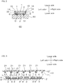
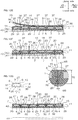
- FIGS. 1A to 1E show process drawings for illustrating one example of a method for producing a light reflecting layer-including optical semiconductor element, not forming part of the invention
- the up-down direction of the paper surface is an up-down direction (first direction, one example of thickness direction)
- the upper side of the paper surface is an upper side (one side in the first direction, one side in the thickness direction)
- the lower side of the paper surface is a lower side (the other side in the first direction, the other side in the thickness direction).
- the right-left direction of the paper surface is a right-left direction (second direction perpendicular to the first direction, one example of the direction perpendicular to the thickness direction)
- the left side of the paper surface is a left side (one side in the second direction)
- the right side of the paper surface is a right side (the other side in the second direction).
- the paper thickness direction is a front-rear direction (third direction perpendicular to the first and second directions, one example of the direction perpendicular to the thickness direction), the near side of the paper surface is a front side (one side in the third direction), and the far side of the paper surface is a rear side (the other side in the third direction).
- the directions are in conformity with direction arrows in each figure.
- the first example includes a temporarily fixing step (ref: FIG. 1A ), a light reflecting sheet filling step (ref: FIG. 1B ), a first attaching portion removing step (ref: FIG. 1C ), a cutting step (ref: FIG. 1D ), and a peeling step (ref: FIG. 1E ).
- a temporarily fixing step (ref: FIG. 1A )
- a light reflecting sheet filling step (ref: FIG. 1B )
- a first attaching portion removing step (ref: FIG. 1C )
- a cutting step (ref: FIG. 1D )
- a peeling step (ref: FIG. 1E ).
- the temporarily fixing step is a step in which a plurality of optical semiconductor elements 1 are temporarily fixed to a temporarily fixing sheet 2 at spaced intervals to each other.
- the optical semiconductor element 1 is, for example, an LED or an LD that converts electrical energy to light energy.
- the optical semiconductor element 1 is a blue LED (light emitting diode element) that emits blue light.
- the optical semiconductor element 1 does not include a rectifier (semiconductor element) such as a transistor that has a different technical field from the optical semiconductor element.
- the optical semiconductor element 1 has a generally flat plate shape along the front-rear and right-left directions.
- the optical semiconductor element 1 has an electrode surface 3, a light emitting surface 4, and peripheral side surfaces 5 as one example of the connecting surface.
- the electrode surface 3 is the lower surface of the optical semiconductor element 1, and is a surface on which an electrode 6 is formed.
- the light emitting surface 4 is the upper surface of the optical semiconductor element 1, and is disposed above the electrode surface 3 in spaced apart relation to oppose thereto.
- the light emitting surface 4 has a flat shape.
- a light emitting layer 7 that is disposed in the upper portion of the optical semiconductor element 1 is provided. In FIGS. 1B to 1E , the light emitting layer 7 is omitted so as to clearly show the relative arrangement of the optical semiconductor element 1 and a light reflecting layer 14 to be described later.
- peripheral side surfaces 5 connect the peripheral end edge of the electrode surface 3 to that of the light emitting surface 4.
- the size of the optical semiconductor element 1 is appropriately set, and to be specific, the optical semiconductor element 1 has a thickness (height) of, for example, 0.1 ⁇ m or more, preferably 0.2 ⁇ m or more, and for example, 500 ⁇ m or less, preferably 200 ⁇ m or less.
- the optical semiconductor element 1 has a length L1 in the front-rear direction and/or the right-left direction of, for example, 0.2 mm or more, preferably 0.5 mm or more, and for example, 3.00 mm or less, preferably 2.00 mm or less.
- the temporarily fixing sheet 2 includes a supporting board 8 and a pressure-sensitive adhesive layer 9 that is disposed on the supporting board 8.
- the supporting board 8 examples include polymer films such as polyethylene film and polyester film (PET and the like), ceramic sheets, and metal foils.
- the supporting board 8 has a thickness of, for example, 1 ⁇ m or more, preferably 10 ⁇ m or more, and for example, 2000 ⁇ m or less, preferably 1000 ⁇ m or less.
- the pressure-sensitive adhesive layer 9 is disposed on the entire upper surface of the supporting board 8.
- the pressure-sensitive adhesive layer 9 has a sheet shape on the upper surface of the supporting board 8.
- the pressure-sensitive adhesive layer 9 is, for example, formed from a pressure-sensitive adhesive in which the pressure-sensitive adhesive force is reduced by treatment (for example, application of ultraviolet rays, heating, or the like).
- a supporting layer (not shown) for improving the mechanical strength of the pressure-sensitive adhesive layer 9 may be interposed midway in the thickness direction thereof.
- the supporting layer include polymer films such as polyethylene film and polyester film (PET and the like).
- the pressure-sensitive adhesive layer 9 has a total thickness of, for example, 1 ⁇ m or more, preferably 10 ⁇ m or more, and for example, 1000 ⁇ m or less, preferably 500 ⁇ m or less.
- the plurality of optical semiconductor elements 1 are temporarily fixed onto the temporarily fixing sheet 2 at spaced intervals to each other in the front-rear and right-left directions.
- the electrode surfaces 3 of the plurality of optical semiconductor elements 1 pressure-sensitively adhere to the upper surface of the pressure-sensitive adhesive layer 9 so as to ensure a gap L0 and a pitch L2 to be described next.
- the plurality of optical semiconductor elements 1 are temporarily fixed to the temporarily fixing sheet 2 so that the light emitting layers 7 face upwardly.
- the electrodes 6 are in contact with the pressure-sensitive adhesive layer 9.
- the electrode surfaces 3 other than the electrodes 6 may be also in contact with the pressure-sensitive adhesive layer 9.
- the gap (gap in the front-rear direction and/or the right-left direction) L0 between the optical semiconductor elements 1 that are next to each other is, for example, 0.05 mm or more, preferably 0.1 mm or more, and for example, 1.50 mm or less, preferably 0.80 mm or less.
- the pitch L2 of the optical semiconductor elements 1 that are next to each other, to be specific, the sum (L1 + L0) of the length L1 and the gap L0 described above is, for example, 0.25 mm or more, preferably 0.60 mm or more, and for example, 3.00 mm or less, preferably 2.00 mm or less.
- the plurality of optical semiconductor elements 1 are supported by the supporting board 8 via the pressure-sensitive adhesive layer 9.
- First gaps 10 are formed between the optical semiconductor elements 1 that are next to each other.
- the first gap 10 has a size corresponding to the gap L0, and though not shown in FIG. 1A , has a generally grid pattern shape when viewed from the top.
- the light reflecting sheet filling step is performed after the temporarily fixing step (ref: FIG. 1A ).
- a light reflecting sheet 11 fills the first gaps 10.
- the light reflecting sheet 11 is included in a light reflecting member 13.
- the light reflecting member 13 includes a peeling sheet 12, and the light reflecting sheet 11 that is supported by the peeling sheet 12.
- the light reflecting member 13 consists of only the peeling sheet 12 and the light reflecting sheet 11.
- the peeling sheet 12 is made of the same material as that of the above-described supporting board 8, and has a layer (flat plate) shape continuing in the front-rear and right-left directions.
- the peeling sheet 12 has a thickness of, for example, 1 ⁇ m or more, preferably 10 ⁇ m or more, and for example, 2000 ⁇ m or less, preferably 1000 ⁇ m or less.
- the length in the front-rear direction and the length in the right-left direction of the peeling sheet 12 are set larger than or the same as those of the light reflecting sheet 11 to be described next.
- the light reflecting sheet 11 is disposed on the lower surface of the peeling sheet 12.
- the light reflecting sheet 11 has a layer (flat plate) shape continuing in the front-rear and right-left directions.
- the light reflecting sheet 11 is set to have a size (length in the front-rear direction and length in the right-left direction) that includes the plurality of optical semiconductor elements 1 when the light reflecting member 13 opposes the upper side of the plurality of optical semiconductor elements 1 that are temporarily fixed to the temporarily fixing sheet 2 and they are projected in the thickness direction.
- the volume V1 (that is, the thickness ⁇ the length in the front-rear direction ⁇ the length in the right-left direction of the light reflecting sheet 11) of the light reflecting sheet 11 is preferably set larger than or the same as the total volume V0 of the first gap 10. More preferably, the volume V1 of the light reflecting sheet 11 is larger than the total volume V0 of the first gap 10. In this case, the light reflecting sheet 11 can easily and surely fill the first gaps 10.
- the volume V1 of the light reflecting sheet 11 with respect to the total volume V0 of the first gap 10 is, for example, 95% or more, preferably 103% or more, and for example, 120% or less, preferably 110% or less.
- the light reflecting sheet 11 has a thickness of, for example, 50 ⁇ m or more, preferably 100 ⁇ m or more, and for example, 1000 ⁇ m or less, preferably 450 ⁇ m or less.
- the light reflecting sheet 11 is, for example, prepared from a light reflecting composition containing a light reflecting component and a resin.
- Examples of the light reflecting component include light reflecting particles such as inorganic particles and organic particles.
- the inorganic particles include oxides such as titanium oxide, zinc oxide, zirconium oxide, and complex inorganic oxide particles (glass or the like); carbonates such as white lead (basic lead carbonate) and calcium carbonate; and clay minerals such as kaolin.
- oxides such as titanium oxide, zinc oxide, zirconium oxide, and complex inorganic oxide particles (glass or the like); carbonates such as white lead (basic lead carbonate) and calcium carbonate; and clay minerals such as kaolin.
- an oxide is used.
- organic particles examples include acrylic resin particles, styrene resin particles, acrylic-styrene resin particles, silicone resin particles, polycarbonate resin particles, benzoguanamine resin particles, polyolefin resin particles, polyester resin particles, polyamide resin particles, and polyimide resin particles.
- acrylic resin particles are used.
- the content ratio of the light reflecting component with respect to the light reflecting composition is, for example, 1 mass% or more, preferably 3 mass% or more, and for example, 80 mass% or less, preferably 75 mass% or less.
- the resin is a matrix that uniformly disperses the light reflecting component in the light reflecting composition, and is, for example, a component that imparts the viscosity (described later) in which the first gaps 10 can be filled with the light reflecting sheet 11 by heating to the light reflecting sheet 11.
- the resin include curing resins and thermoplastic resins.
- a curing resin is used.
- the curing resin include thermosetting resins such as two-step reaction curing resin and one-step reaction curing resin.
- the two-step reaction curing resin has two reaction mechanisms, and in the first-step reaction, the resin can be brought from an A-stage state into a B-stage state (semi-cured) and next, in the second-step reaction, the resin can be brought from the B-stage state into a C-stage state (completely cured). That is, the two-step reaction curing resin is a thermosetting resin that can be brought into the B-stage state in accordance with appropriate heating conditions.
- the B-stage state is a state between the A-stage state in which the thermosetting resin is liquid and the C-stage state in which the thermosetting resin is completely cured.
- the B-stage state is also a semi-solid state or solid state in which curing and gelation are slightly progressed, and the compressive elastic modulus thereof is smaller than that of the C-stage state.
- the one-step reaction curing resin has one reaction mechanism, and in the first-step reaction, the resin can be brought from an A-stage state into a C-stage state (completely cured).
- This one-step reaction curing resin includes a thermosetting resin in which its reaction can be terminated midway of the first-step reaction to be brought from the A-stage state to a B-stage state, and by subsequent further heating, the first-step reaction can be restarted to be brought from the B-stage state to the C-stage state (completely cured). That is, the thermosetting resin includes the thermosetting resin that can be brought into the B-stage state.
- the one-step reaction curing resin can also include a thermosetting resin that cannot control termination midway of the one-step reaction, that is, cannot be brought into the B-stage state and is brought from the A-stage state to the C-stage state (completely cured) at one time.
- thermosetting resin a thermosetting resin that can be brought into a B-stage state is used.
- thermosetting resin examples include silicone resin, epoxy resin, urethane resin, polyimide resin, phenol resin, urea resin, melamine resin, and unsaturated polyester resin.
- a silicone resin and an epoxy resin are used, more preferably, a silicone resin is used.
- silicone resin examples include phenyl silicone resins that include a phenyl group in a molecule and methyl silicone resins that include a methyl group in a molecule.
- the phenyl silicone resin in the B-stage state is once melted or liquefied by heating and then, completely cured. Meanwhile, the methyl silicone resin in the B-stage state is once softened or plasticized by heating and then, completely cured.
- the phenyl silicone resin in the B-stage state easily forms a first attaching portion 17 (described later) in the light reflecting sheet filling step shown in FIG. 1B compared to the methyl silicone resin in the B-stage state.
- the viscosity of the silicone resin in the B-stage state is gradually reduced along with the temperature rising, and thereafter, along with the continuous temperature rising, the viscosity thereof is gradually increased to be brought into the silicone resin in the C-stage state.
- thermosetting resin may be the same kind or a plurality of kinds.
- the mixing ratio of the resin with respect to the light reflecting composition is, for example, 10 mass% or more, preferably 25 mass% or more, and for example, 99 mass% or less, preferably 97 mass% or less.
- the light reflecting composition can also contain an additive at an appropriate ratio.
- the light reflecting sheet 11 for example, first, a light reflecting component, a resin, and an additive added as needed, are blended to prepare a varnish of the light reflecting composition. Subsequently, the varnish is applied to the surface of the peeling sheet 12. Thereafter, when the light reflecting composition contains the thermosetting resin that can be brought into the B-stage state, the light reflecting composition is brought into the B-stage state (semi-cured). To be specific, the light reflecting composition is heated.
- the heating temperature is, for example, 50°C or more, preferably 70°C or more, and for example, 120°C or less, preferably 100°C or less.
- the heating time is, for example, 5 minutes or more, preferably 10 minutes or more, and for example, 20 minutes or less, preferably 15 minutes or less.
- the light reflecting sheet 11 is formed.
- the light reflecting sheet 11 in the B-stage state is formed on the surface of the peeling sheet 12.
- the melting viscosity at 60°C of the light reflecting sheet 11 is, for example, 40 Pa ⁇ s or more, and for example, 1000 Pa ⁇ s or less, preferably 300 Pa ⁇ s or less.
- the melting viscosity is measured using an E-type viscometer.
- the melting viscosity at 60°C is the above-described upper limit or less
- the viscosity of the light reflecting sheet 11 is sufficiently reduced by hot pressing (described later), and the light reflecting sheet 11 can quickly and surely fill the first gaps 10.
- the melting viscosity at 60°C is the above-described lower limit or more
- the light reflecting sheet 11 is suppressed to be excessively soft, and the flow of the light reflecting sheet 11 outwardly so as to be apart from the optical semiconductor elements 1 can be suppressed.
- the light reflecting member 13 is compressively bonded to the temporarily fixing sheet 2 and the optical semiconductor elements 1.
- the light reflecting member 13, the temporarily fixing sheet 2, and the optical semiconductor elements 1 are set in a pressing machine so that the light reflecting sheet 11 faces the optical semiconductor elements 1 in the thickness direction to be, for example, hot pressed.
- the conditions of the hot pressing are appropriately set.
- the temperature of the hot pressing is, for example, 60°C or more, preferably 70°C or more, and for example, 200°C or less, preferably 180°C or less.
- the pressure of the hot pressing is, for example, 0.01 MPa or more, preferably 0.10 MPa or more, and for example, 10.00 MPa or less, preferably 5.00 MPa or less.
- the time of the hot pressing is, for example, 1 minute or more, preferably 3 minutes or more, and for example, 60 minutes or less, preferably 30 minutes or less.
- the hot pressing can be performed in a plurality of times.
- the light reflecting sheet 11 (light reflecting composition) can fill the first gaps 10.
- the light reflecting layer 14 made of the light reflecting composition (light reflecting sheet 11) is formed in a shape of filling the first gaps 10.
- portions that fill the first gaps 10 are first filling portions 33.
- the light reflecting layer 14 covers the peripheral side surfaces 5 of the optical semiconductor elements 1. That is, the light reflecting layer 14 is formed on the peripheral side surfaces 5 of the plurality of optical semiconductor elements 1. The light reflecting layer 14 also covers the surfaces that are exposed from the electrodes 6 in the electrode surfaces 3 of the optical semiconductor elements 1. Furthermore, the light reflecting layer 14 covers and is attached to the light emitting surfaces 4 of the optical semiconductor elements 1. In the light reflecting layer 14, portions that are attached to the light emitting surfaces 4 are the first attaching portions 17.
- the light reflecting layer 14 has a flat upper surface 15.
- the upper surface 15 of the first attaching portion 17 is flush with the upper surface 15 of the portion (portion positioned between the first attaching portions 17 that are next to each other) that is positioned on the first filling portion 33 in the front-rear and right-left directions.
- the first attaching portion 17 has a thickness T1 of, for example, 1 ⁇ m or more, and for example, 500 ⁇ m or less, furthermore, 200 ⁇ m or less.
- the peeling sheet 12 is peeled from the light reflecting layer 14.
- the peeling sheet 12 is peeled from the upper surface 15 of the light reflecting layer 14.
- light reflecting layer-including optical semiconductor elements 16, each of which includes the optical semiconductor element 1, and the light reflecting layer 14 that has the first filling portion 33 and the first attaching portion 17, are obtained in a state where the electrode surfaces 3 are temporarily fixed to the temporarily fixing sheet 2.
- the upper surface of the light reflecting layer-including optical semiconductor element 16 consists of the upper surface 15 of the light reflecting layer 14, and to be specific, the light emitting surface 4 of the optical semiconductor element 1 is covered with the light reflecting layer 14.
- the light reflecting layer-including optical semiconductor elements 16, each of which includes the optical semiconductor element 1 and the light reflecting layer 14, are obtained in a state of being temporarily fixed to the temporarily fixing sheet 2.
- the first attaching portion removing step is performed after the light reflecting sheet filling step (ref: FIG. 1B ).
- the first attaching portion removing step the first attaching portions 17 are removed.
- the pressure-sensitive adhesive sheet 18 is prepared from a pressure-sensitive adhesive, and has a sheet shape continuing in the front-rear and right-left directions.
- the size of the pressure-sensitive adhesive sheet 18 is, for example, set to be capable of including the first attaching portions 17 when projected in the thickness direction.
- Examples of the pressure-sensitive adhesive include acrylic pressure-sensitive adhesive, rubber pressure-sensitive adhesive, silicone pressure-sensitive adhesive, urethane pressure-sensitive adhesive, and polyacrylamide pressure-sensitive adhesive.
- the pressure-sensitive adhesive sheet 18 may be supported by a supporting member or the like.
- the pressure-sensitive adhesive force at 25°C (180° peeling adhesive force) of the pressure-sensitive adhesive sheet 18 is, for example, 7.5 (N/20 mm) or more, preferably 10.0 (N/20 mm) or more, and for example, 100 (N/20 mm) or less, preferably 20.0 (N/20 mm) or less.
- the pressure-sensitive adhesive force is measured as the adhesive force when the pressure-sensitive adhesive sheet 18 is cut into a piece having a width of 20 mm to then pressure-sensitively adhere to a silicone wafer, and thereafter, the pressure-sensitive adhesive sheet 18 is subjected to a peeling test at a peeling rate of 100 mm/min and a peeling angle of 180°.
- a pressure-sensitive adhesive surface in a case where the pressure-sensitive adhesive sheet 18 is supported by a supporting member, first, the opposite-side surface to the surface supported by the supporting member
- the pressure-sensitive adhesive sheet 18 is disposed to oppose the upper surface 15 of the light reflecting layer 14 including the first attaching portions 17 to pressure-sensitively adhere to the first attaching portions 17 and subsequently, the first attaching portions 17 are peeled from the light emitting surfaces 4.
- the pressure-sensitive adhesive sheet 18 is lowered, subsequently, as shown by the central portion of FIG.
- the pressure-sensitive adhesive sheet 18 pressure-sensitively adheres to the first attaching portions 17, and thereafter, as shown by the left-side portion of FIG. 1B , the pressure-sensitive adhesive sheet 18 is raised (lifted up) along with the first attaching portions 17.
- the first attaching portions 17 are peeled at the interfaces between the first attaching portions 17 and the light emitting surfaces 4 to then follow the pressure-sensitive adhesive sheet 18. Also, when the peeling of the first attaching portions 17 is not completed at a time, the above-described action is repeated in a plurality of times, so that the peeling of the first attaching portions 17 is completed. At this time, in the light reflecting layer 14, the portions that are positioned on the first filling portions 33, along with the first attaching portions 17, follow the pressure-sensitive adhesive sheet 18. That is, in the light reflecting layer 14, the first attaching portions 17 and the portions that are positioned on the first filling portions 33 are removed.
- portions 34 that are positioned at the upper side of the light emitting surfaces 4 are removed.
- the upper surface 15 of the first filling portion 33 is flush with the light emitting surface 4 in the front-rear and right-left directions. That is, the upper surface 15 of the first filling portion 33 and the light emitting surface 4 form the same flat surface.
- the resin is the thermosetting resin (thermosetting resin in the B-stage state)
- the light reflecting layer 14 is cured by heating (completely cured).
- the heating temperature is, for example, 100°C or more, preferably 120°C or more, and for example, 200°C or less, preferably 150°C or less.
- the heating time is, for example, 10 minutes or more, preferably 30 minutes or more, and for example, 180 minutes or less, preferably 120 minutes or less.
- a solvent and the pressure-sensitive adhesive sheet 18 are used in combination.
- a solvent that can completely or partially dissolve or disperse the light reflecting composition that forms the first attaching portion 17 is selected.
- the solvent include organic solvents and aqueous solvents.
- the organic solvent include alcohols such as methanol and ethanol, ketones such as acetone and methyl ethyl ketone, aliphatic hydrocarbons such as hexane, aromatic hydrocarbons such as toluene, and ethers such as tetrahydrofuran.
- an alcohol and an aromatic hydrocarbon are used.
- the pressure-sensitive adhesive sheet 18 described in (1) is used as the pressure-sensitive adhesive sheet 18.
- the resin is the thermosetting resin (thermosetting resin in the B-stage state)
- the light reflecting layer 14 is cured by heating (completely cured).
- the above-described solvent is absorbed in cloth, and the upper surface 15 of the cured light reflecting layer 14 is wiped by the cloth.
- the solvent even when the upper surface 15 of the light reflecting layer 14 is wiped, the first attaching portion 17 remains.
- the remaining first attaching portion 17 is removed using the pressure-sensitive adhesive sheet 18 described in (1).
- polishing member examples include cloth such as buff, brushes, and water blasting.
- the polishing member By the polishing member, the upper surface 15 of the light reflecting layer 14 of the light reflecting layer-including optical semiconductor element 16 is polished. In this manner, the upper layer portion 34 including the first attaching portion 17 is removed.
- the timing of polishing of the upper surface 15 by the polishing member may be before or after the curing of the light reflecting layer 14.
- the cutting step is performed after the first attaching portion removing step (ref: FIG. 1C ).
- the light reflecting layers 14 are cut between the optical semiconductor elements 1 that are next to each other. That is, in the cutting step, the first filling portions 33 are cut. In this manner, in the light reflecting layer-including optical semiconductor elements 16, the plurality of optical semiconductor elements 1 are singulated.
- a cutting device such as a dicing device using a disk-shaped dicing saw (dicing blade) 19, a cutting device using a cutter, and a laser application device is used.
- a dicing device is used.
- the dicing saw 19 has a blade thickness T3 of, for example, 10 ⁇ m or more, preferably 20 ⁇ m or more, and for example, 200 ⁇ m or less, preferably 100 ⁇ m or less.
- cut ditches 20 By cutting the light reflecting layers 14 (first filling portions 33), in the light reflecting layers 14, cut ditches 20 in alignment along the front-rear and right-left directions are formed between the optical semiconductor elements 1 that are next to each other.
- the cut ditches 20 pass through the light reflecting layers 14 in the thickness direction.
- the cut ditches 20 have a generally grid pattern shape when viewed from the top.
- the cut ditch 20 may be formed in the pressure-sensitive adhesive layer 9. In such a case, the lower end portion of the cut ditch 20 reaches the middle in the thickness direction of the pressure-sensitive adhesive layer 9. That is, the cut ditch 20 is cut out in both of the light reflecting layer 14 and the pressure-sensitive adhesive layer 9.
- a width W1 of the cut ditch 20 corresponds to the cutting device (preferably, the blade thickness T3 of the dicing saw 19) and, to be specific, is, for example, 10 ⁇ m or more, preferably 20 ⁇ m or more, and for example, 200 ⁇ m or less, preferably 100 ⁇ m or less.
- the peeling step is performed after the cutting step (ref. FIG. 1D ).
- the supporting board 8 is peeled from the pressure-sensitive adhesive layer 9.
- the plurality of light reflecting layer-including optical semiconductor elements 16 that are disposed in alignment at spaced intervals (width W1) to each other in the front-rear and right-left directions are obtained in a state of being supported by the pressure-sensitive adhesive layer 9.
- each of the light reflecting layer-including optical semiconductor elements 16 is peeled from the pressure-sensitive adhesive layer 9.
- a pick-up device including a collet and a suction pump connected thereto or the like is used.
- the collet is brought into contact with the light emitting surface 4, subsequently, the suction pump is driven, and next, the collet is pulled up.
- the light reflecting layer-including optical semiconductor elements 16, each of which includes one optical semiconductor element 1, and the light reflecting layer 14 that covers the peripheral side surfaces 5 and exposes the light emitting surface 4 of the optical semiconductor element 1, are obtained.
- the light reflecting layer-including optical semiconductor element 16 consists of only the optical semiconductor element 1 and the light reflecting layer 14.
- the side surface 32 of the light reflecting layer 14 is exposed laterally, the light emitting surface 4 and the upper surface 15 of the light reflecting layer 14 that is positioned around the light emitting surface 4 are exposed upwardly, and the lower surface of the electrode 6 is exposed downwardly.
- the light emitting surface 4 of the optical semiconductor element 1 is flush with the upper surface 15 of the light reflecting layer 14.
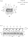
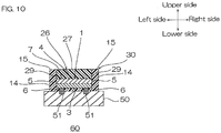
- the light reflecting layer-including optical semiconductor element 16 is not an optical semiconductor device 60 (ref: FIG. 2 ) to be described next, that is, does not include a board 50 included in the optical semiconductor device 60. That is, in the light reflecting layer-including optical semiconductor element 16, the electrode 6 is not electrically connected to terminals 51 provided in the board 50. That is, the light reflecting layer-including optical semiconductor element 16 is a component of the optical semiconductor device 60, that is, a component to produce the optical semiconductor device 60 and a device that allows the component alone to be distributed and industrially available.
- the electrode 6 of the light reflecting layer-including optical semiconductor element 16 is electrically connected to the terminals 51 provided on the upper surface of the board 50.
- the light reflecting layer-including optical semiconductor element 16 is flip-chip mounted on the board 50.
- the optical semiconductor device 60 including the light reflecting layer-including optical semiconductor element 16 and the board 50 is obtained. That is, the optical semiconductor device 60 includes the board 50, the optical semiconductor element 1 mounted on the board 50, and the light reflecting layer 14 that covers the peripheral side surfaces 5 of the optical semiconductor element 1.
- the optical semiconductor device 60 preferably consists of only the board 50, the optical semiconductor element 1, and the light reflecting layer 14.
- the light emitting layer 7 is positioned at the upper portion of the optical semiconductor element 1, and the light emitting surface 4 is exposed from the light reflecting layer 14 upwardly.
- the light reflecting layers 14 that are attached to the light emitting surfaces 4 of the plurality of optical semiconductor elements 1, that is, the first attaching portions 17 are removed, so that light that is emitted from the light emitting surfaces 4 of the plurality of optical semiconductor elements 1 can be efficiently taken out.
- the light reflecting sheet 11 has a shape continuing in the front-rear and right-left directions so as to include the plurality of optical semiconductor elements 1 when projected in the thickness direction, so that as shown in FIG. 1B , the light reflecting sheet 11 can easily fill the first gaps 10 (ref: FIG. 1A ).
- Second Attaching Portion Removing Step first, after second attaching portions 31 in the light reflecting layer 14 are removed using the pressure-sensitive adhesive sheet 18, when the resin contained in the light reflecting layer 14 is the thermosetting resin (thermosetting resin in the B-stage state), the light reflecting layer 14 is cured by heating (completely cured). Alternatively, for example, first, the light reflecting layer 14 is cured by heating (completely cured) and thereafter, the second attaching portions 31 in the light reflecting layer 14 can be also removed using the pressure-sensitive adhesive sheet 18.
- the solvent and the pressure-sensitive adhesive sheet 18 are used in combination.
- the second attaching portions 31 in the light reflecting layer 14 can be sufficiently removed by the solvent, the second attaching portions 31 in the light reflecting layer 14 can be also removed by only the solvent.
- the light reflecting sheet 11 has a layer (flat plate) shape continuing in the front-rear and right-left directions at the lower surface of the peeling sheet 12.
- the light reflecting sheet 11 can also have a pattern shape corresponding to the first gaps 10.
- a plurality of opening portions 21 are formed in the light reflecting sheet 11.
- the opening portions 21 have the same shapes as the outer shapes of the optical semiconductor elements 1 when projected in the thickness direction. Meanwhile, the light reflecting sheet 11 has the same shape as that of the first gap 10 when projected in the thickness direction.
- the light reflecting layer 14 is attached to the light emitting surfaces 4 to form the first attaching portions 17.
- the light reflecting sheet 11 shown in FIG. 1A in the first example easily causes the first attaching portions 17 (ref: FIG. 1B ), that is, easily causes the problem described above.
- the cutting step (ref: FIG. 1D ) is performed after the first attaching portion removing step (ref: FIG. 1C ).
- the first attaching portion removing step (ref: FIG. 1C ) can be also performed after the cutting step (ref: FIG. 1D ).
- the cutting step (ref: FIG. 1D ) is performed after the first attaching portion removing step (ref: FIG. 1C ).
- the first attaching portion removing step (ref: FIG. 1C ) is performed after the cutting step (ref: FIG. 1D ) by "(1) Method Using Pressure-Sensitive Adhesive Sheet 18" and/or "(3) Method Using Polishing Member"
- the pressure-sensitive adhesive of the pressure-sensitive adhesive sheet 18 and/or the polishing member enter(s) the cut ditches 20 (ref: FIG. 1D ) formed in the cutting step, so that the first filling portions 33 (light reflecting layer 14 that covers the peripheral side surfaces 5) are removed by the pressure-sensitive adhesive sheet 18 and/or the polishing member.
- the above-described possibility can be eliminated.
- the solvent may enter the cut ditches 20 formed in the cutting step to remain.
- a step of removing the solvent is separately required.
- the above-described possibility can be eliminated.
- the light reflecting sheet filling step for example, as shown in FIG. 1B , when the light reflecting layer 14 in the B-stage (semi-cured) state including the first attaching portions 17 is formed, by controlling the filling temperature and time of the light reflecting sheet 11, "(2) Method Using Solvent" can be used.
- the hardness of the light reflecting sheet 11 in the B-stage state is set, for example, 95 or more and 99 or less.
- the hardness of the light reflecting sheet 11 is, for example, calculated using a soft material hardness meter (manufactured by CITIZEN SEIMITSU CO., LTD., CH-R01, diameter of sensor head: 2 mm).
- a soft material hardness meter manufactured by CITIZEN SEIMITSU CO., LTD., CH-R01, diameter of sensor head: 2 mm.
- a soft material hardness meter 71 is prepared.
- the soft material hardness meter 71 includes a plunger 74 that extends in the up-down direction, a sensor head 72 that is provided at the lower end portion of the plunger 74, a cylinder 73 that houses the plunger 74, and a processing device (not shown) that is connected to the sensor head 72 and configured to be capable of detecting the position of the sensor head 72.
- the sensor head 72 has a generally spherical shape.
- the lower end portion of the cylinder 73 and the lower end portion of the sensor head 72 are brought into contact with the surface of the light reflecting sheet 11 that is disposed on the peeling sheet 12.
- Hardness 1 ⁇ distance d at which the sensor head 72 sinks sinking of full load ⁇ sinking of initial load ⁇ m / 300 reference value ⁇ m ⁇ 100
- the filling time of the light reflecting sheet 11 is appropriately set in accordance with the filling temperature.
- the filling time of the light reflecting sheet 11 is, for example, 250 seconds or more and 600 seconds or less.
- the filling temperature of the light reflecting sheet 11 is 90°C, the filling time of the light reflecting sheet 11 is, for example, 400 seconds or more and 750 seconds or less.
- the filling temperature of the light reflecting sheet 11 is 80°C, the filling time of the light reflecting sheet 11 is, for example, 800 seconds or more and 1000 seconds or less.
- the first attaching portions 17 when the first attaching portions 17 are removed by "(2) Method Using Solvent" (described later), the first attaching portions 17 can be more surely removed.
- the peeling step is performed.
- the peeling step may not be performed. That is, as shown in FIG. 1D , the plurality of light reflecting layer-including optical semiconductor elements 16, each of which includes a singulated optical semiconductor element 1 and the light reflecting layer 14 in a state of being supported by the temporarily fixing sheet 2 (supporting board 8 and pressure-sensitive adhesive layer 9), are also a component to produce the optical semiconductor device 60, and used as a device that allows the component alone to be distributed and industrially available.
- the supporting board 8 in the peeling step shown in FIG. 1E can be also removed. That is, as shown by the solid lines of FIG. 1E , the plurality of light reflecting layer-including optical semiconductor elements 16 in a state of being supported by only the pressure-sensitive adhesive layer 9 are also a component to produce the optical semiconductor device 60, and used as a device that allows the component alone to be distributed and industrially available.
- a phosphor layer or the like can be also provided in the light emitting surface 4 in each of the light reflecting layer-including optical semiconductor elements 16 shown in FIG. 1E .
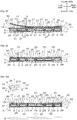
- the second example of the description includes a temporarily fixing step (ref: FIG. 4A ), a phosphor layer forming step (ref: FIGS. 4B and 4C ), a light reflecting sheet filling step (ref: FIG. 4D ), a second attaching portion removing step (ref: FIG. 5E ), a cutting step (ref: FIG. 5F ), and a peeling step (ref: FIG. 5G ).
- a temporarily fixing step (ref: FIG. 4A )
- a phosphor layer forming step (ref: FIGS. 4B and 4C )
- a light reflecting sheet filling step (ref: FIG. 4D )
- a second attaching portion removing step (ref: FIG. 5E )
- a cutting step (ref: FIG. 5F )
- a peeling step (ref: FIG. 5G ).
- the temporarily fixing step is a step in which the plurality of optical semiconductor elements 1 are temporarily fixed to the temporarily fixing sheet 2 at spaced intervals to each other.
- the phosphor layer forming step is performed after the temporarily fixing step (ref: FIG. 4A ).
- phosphor layers 26 are formed in the light emitting surfaces 4 and the peripheral side surfaces 5 of the plurality of optical semiconductor elements 1 so that second gaps 23 are formed between the optical semiconductor elements 1 that are next to each other.
- a phosphor sheet 24 is prepared.
- the phosphor sheet 24 is included in a phosphor member 25.
- the phosphor member 25 includes the peeling sheet 12 and the phosphor sheet 24 that is supported by the peeling sheet 12.
- the phosphor member 25 consists of only the peeling sheet 12 and the phosphor sheet 24.
- the phosphor sheet 24 is formed on the lower surface of the peeling sheet 12, and has a layer (flat plate) shape continuing in the front-rear and right-left directions.
- the phosphor sheet 24 is, for example, prepared from a phosphor composition containing a phosphor and a resin.
- the phosphor converts the wavelength of light that is emitted from the optical semiconductor element 1.
- Examples of the phosphor include a yellow phosphor that is capable of converting blue light into yellow light and a red phosphor that is capable of converting blue light into red light.
- yellow phosphor examples include silicate phosphors such as (Ba, Sr, Ca)2 SiO4 :Eu and (Sr, Ba)2 SiO4 :Eu (barium orthosilicate (BOS)); garnet-type phosphors having a garnet-type crystal structure such as Y3 Al5 O12 :Ce (YAG (yttrium aluminum garnet):Ce) and Tb3 A13 012 :Ce (TAG (terbium aluminum garnet):Ce); and oxynitride phosphors such as Ca- ⁇ -SiAlON.
- silicate phosphors such as (Ba, Sr, Ca)2 SiO4 :Eu and (Sr, Ba)2 SiO4 :Eu
- BOS barium orthosilicate
- garnet-type phosphors having a garnet-type crystal structure such as Y3 Al5 O12 :Ce (YAG (yttrium aluminum garnet):Ce)
- red phosphor examples include nitride phosphors such as CaAlSiN3 :Eu and CaSiN2 :Eu.
- a yellow phosphor is used, more preferably, a garnet-type phosphor is used.
- Examples of the shape of the phosphor include a sphere shape, a plate shape, and a needle shape.
- the average value of the maximum length (in the case of a sphere shape, the average particle size) of the phosphor is, for example, 0.1 ⁇ m or more, preferably 1 ⁇ m or more, and for example, 200 ⁇ m or less, preferably 100 ⁇ m or less.
- the phosphors can be used alone or in combination.
- the mixing ratio of the phosphor with respect to the phosphor composition is, for example, 5 mass% or more, preferably 10 mass% or more, and for example, 80 mass% or less, preferably 70 mass% or less.
- the resin is a matrix that uniformly disperses the phosphor in the phosphor composition, and is, for example, a component that imparts the viscosity in which the first gaps 10 can be filled with the phosphor sheet 24 by heating to the phosphor sheet 24.
- the resin is the same as that contained in the light reflecting composition in the first example.
- the mixing ratio of the resin is the remaining portion of the mixing ratio of the phosphor (and light reflecting component and/or additive to be described next).
- the phosphor composition can also contain a light reflecting component and/or an additive at an appropriate ratio.
- the phosphor sheet 24 for example, a phosphor, a resin, and a light reflecting component and/or an additive added as needed, are blended to prepare a varnish of the phosphor composition. Subsequently, the varnish is applied to the surface of the peeling sheet 12. Thereafter, when the phosphor composition contains the thermosetting resin that can be brought into the B-stage state, the phosphor composition is brought into the B-stage state (semi-cured). To be specific, the phosphor composition is heated. In this manner, the phosphor sheet 24 is formed.
- the properties (shear storage elastic modulus G' or the like) of the phosphor sheet 24 are appropriately selected from the properties of the light reflecting composition in the first example.
- the phosphor sheet 24 has a thickness of, for example, 50 ⁇ m or more, preferably 100 ⁇ m or more, and for example, 1000 ⁇ m or less, preferably 450 ⁇ m or less. As shown in FIG. 1A , the phosphor sheet 24 is set to have a size (length in the front-rear direction and length in the right-left direction) that includes the plurality of optical semiconductor elements 11 when the light reflecting member 13 opposes the upper side of the plurality of optical semiconductor elements 11 that are temporarily fixed to the temporarily fixing sheet 2 and they are projected in the thickness direction.
- the phosphor member 25 is hot pressed with respect to the temporarily fixing sheet 2.
- the phosphor sheet 24 (phosphor composition) fills the first gaps 10 (phosphor sheet filling step).
- portions filling the first gaps 10 are second filling portions 35.
- the phosphor sheet 24 opposing the plurality of optical semiconductor elements 1 covers the light emitting surfaces 4 of the plurality of optical semiconductor elements 1.
- the phosphor layers 26 are formed from the phosphor sheet 24 on the light emitting surfaces 4 and the peripheral side surfaces 5 of the plurality of optical semiconductor elements 1.
- the phosphor layers 26 embed the plurality of optical semiconductor elements 1.
- the phosphor layers 26 have a shape continuing in the front-rear and right-left directions. Furthermore, each of the phosphor layers 26 has an upper surface 27 as one example of a flat surface.
- the phosphor layers 26 cover the surfaces exposed from the electrodes 6 in the electrode surfaces 3 of the optical semiconductor elements 1.
- the phosphor layers 26 are cut between the optical semiconductor elements 1 that are next to each other.
- the dicing saw 28 has the same width (same blade thickness T4) from the inner side gradually toward the outer side in a radial direction.
- the blade thickness T4 of the dicing saw 28 is thicker than the blade thickness T3 (ref: FIG. 1D ) of the dicing saw 19 that cuts the light reflecting layer 14 in the first example.
- the blade thickness T4 of the dicing saw 28 with respect to the blade thickness T3 of the dicing saw 19 is, for example, 150% or more, preferably 200% or more, more preferably 300% or more, and for example, 10000% or less.
- the blade thickness T4 of the dicing saw 28 is appropriately set corresponding to a width W2 (ref: FIG. 4C ) of the second gap 23 to be described next, and is, for example, 100 ⁇ m or more, preferably 200 ⁇ m or more, and for example, 2000 ⁇ m or less, preferably 1000 ⁇ m or less.
- the phosphor layers 26 between the optical semiconductor elements 1 that are next to each other are cut (phosphor layer removing step).
- the second gaps 23 are formed in the phosphor layers 26.
- the second gaps 23 pass through the phosphor layers 26 in the thickness direction.
- the second gaps 23 are formed in the second filling portions 35 and portions that are positioned on the second filling portions 35 in the phosphor layers 26.
- the second gaps 23 have a generally grid pattern shape when viewed from the top.
- the cross-sectional shape of the opening and the cross-sectional area of the opening in the lower end portion are the same as those in the upper end portion.
- a width W3 of the phosphor layer 26 that is formed on the peripheral side surface 5 is adjusted to a desired size. That is, in the cutting of the phosphor layer 26 that is formed on the peripheral side surface 5, the phosphor layer 26 is trimmed so that the width W3 of the phosphor layer 26 is a predetermined size.
- the width W3 of the phosphor layer 26 that is formed on the peripheral side surface 5 is, for example, 50 ⁇ m or more, preferably 100 ⁇ m or more, and for example, 2000 ⁇ m or less, preferably 1000 ⁇ m or less.
- the width W3 of the phosphor layer 26 is the same over the thickness direction.
- the second gap 23 has the width W2 of, for example, 100 ⁇ m or more, preferably 200 ⁇ m or more, and for example, 2000 ⁇ m or less, preferably 1000 ⁇ m or less.
- the width W2 of the second gap 23 is the same over the thickness direction.
- the plurality of phosphor layers 26 are formed corresponding to the plurality of optical semiconductor elements 1 in a pattern covering the light emitting surfaces 4 and the peripheral side surfaces 5 of the plurality of optical semiconductor elements 1.
- Each of the plurality of phosphor layers 26 has a generally U-shape having an opening downwardly when viewed in cross section.
- the light reflecting sheet filling step is performed after the phosphor layer forming step (ref: FIGS. 4B and 4C ).
- the light reflecting sheet 11 (ref: FIG. 4C ) fills the second gaps 23.
- the light reflecting sheet 11 is the same as that of the first example.
- the light reflecting member 13, the temporarily fixing sheet 2, the optical semiconductor elements 1, and the phosphor layers 26 are set in a pressing machine so that the light reflecting sheet 11 opposes the phosphor layers 26 to be, for example, hot pressed.
- the light reflecting sheet 11 fills the second gaps 23.
- the light reflecting layer 14 made of the light reflecting composition is formed in a shape of filling the second gaps 23.
- portions that fill the second gaps 23 are third filling portions 37.
- the light reflecting layer 14 (third filling portion 37) covers peripheral side surfaces 29 of the phosphor layers 26 formed on the peripheral side surfaces 5 of the optical semiconductor elements 1.
- the light reflecting layer 14 covers and is attached to the upper surfaces 27 of the phosphor layers 26 that are formed on the light emitting surfaces 4 of the optical semiconductor elements 1.
- portions that are attached to the upper surfaces 27 of the phosphor layers 26 are the second attaching portions 31.
- the light reflecting layer 14 has the flat upper surface 15.
- the second attaching portion 31 is flush with the portion that is positioned on the third filling portion 37 in the front-rear and right-left directions.
- the second attaching portion 31 has a thickness T2 of, for example, 1 ⁇ m or more, and for example, 50 ⁇ m or less, furthermore, 200 ⁇ m or less.
- the peeling sheet 12 is peeled from the light reflecting layer 14.
- the peeling sheet 12 is peeled from the upper surface 15 of the light reflecting layer 14.
- light reflecting layer and phosphor layer-including optical semiconductor elements 30, each of which includes the optical semiconductor element 1, the phosphor layer 26 that is formed on the light emitting surface 4 and the peripheral side surfaces 5 of the optical semiconductor element 1, and the light reflecting layer 14 that has the third filling portion 37 and the second attaching portion 31, are obtained in a state where the electrode surfaces 3 of the optical semiconductor elements 1 are temporarily fixed to the temporarily fixing sheet 2.
- the second attaching portion removing step is performed after the light reflecting sheet filling step (ref: FIG. 4D ).
- the second attaching portion removing step the second attaching portions 31 are removed.
- the portions that are positioned on the third filling portions 37 are removed along with the second attaching portions 31. That is, in the light reflecting layer 14, when projected in the front-rear and right-left directions, portions 36 that are positioned at the upper side of the upper surfaces 27 of the phosphor layers 26 (upper layer portions 36) are removed.
- the method for removing the second attaching portions 31 is the same as that for removing the first attaching portions 17 illustrated in the first example.
- the light reflecting layer 14 is cured by heating (completely cured).
- the solvent and the pressure-sensitive adhesive sheet 18 are used in combination.
- the resin contained in the light reflecting layer 14 is the thermosetting resin (thermosetting resin in the B-stage state)
- the light reflecting layer 14 is cured by heating (completely cured).
- the above-described solvent is absorbed in cloth, and the upper surface 15 of the cured light reflecting layer 14 is wiped by the cloth.
- the solvent even when the upper surface 15 of the light reflecting layer 14 is wiped, the second attaching portion 31 remains.
- the remaining second attaching portion 31 is removed using the pressure-sensitive adhesive sheet 18 described in (1).
- the timing of polishing of the upper surface 15 by the polishing member may be before or after the curing of the light reflecting layer 14.
- the upper surface 15 of the third filling portion 37 is flush with the upper surface 27 of the phosphor layer 26 in the front-rear and right-left directions. That is, the upper surface 27 of the phosphor layer 26 that is exposed from the light reflecting layer 14 and the upper surface 15 of the third filling portion 37 of the light reflecting layer 14 form the same flat surface.
- the cutting step is performed after the second attaching portion removing step (ref: FIG. 5E ).
- the light reflecting layers 14 are cut between the optical semiconductor elements 1 that are next to each other.
- the third filling portions 37 (ref: FIG. 5E ) are cut.
- the method for cutting the light reflecting layers 14 is the same as that of the first example.
- the cut ditch 20 may be also formed in the pressure-sensitive adhesive layer 9. In such a case, the lower end portion of the cut ditch 20 reaches the middle in the thickness direction of the pressure-sensitive adhesive layer 9. That is, the cut ditch 20 is cut out in both of the light reflecting layer 14 and the pressure-sensitive adhesive layer 9.
- the cut ditches 20 in alignment along the front-rear and right-left directions are formed between the optical semiconductor elements 1 that are next to each other.
- the peeling step is performed after the cutting step (ref. FIG. 5F ).
- the supporting board 8 is peeled from the pressure-sensitive adhesive layer 9.
- the plurality of light reflecting layer and phosphor layer-including optical semiconductor elements 30 that are disposed in alignment at spaced intervals (width W1) to each other in the front-rear and right-left directions are obtained in a state of being supported by the pressure-sensitive adhesive layer 9.
- each of the light reflecting layer and phosphor layer-including optical semiconductor elements 30 is peeled from the pressure-sensitive adhesive layer 9.
- the method for peeling the light reflecting layer and phosphor layer-including optical semiconductor element 30 from the pressure-sensitive adhesive layer 9 is the same as that illustrated in the first example.
- the light reflecting layer and phosphor layer-including optical semiconductor elements 30, each of which includes one optical semiconductor element 1, the phosphor layer 26 that covers the light emitting surface 4 and the peripheral side surfaces 5 of the optical semiconductor element 1, and the light reflecting layer 14 that covers the peripheral side surfaces 29 of the phosphor layer 26, are obtained.
- the light reflecting layer and phosphor layer-including optical semiconductor element 30 consists of only the optical semiconductor element 1, the phosphor layer 26, and the light reflecting layer 14.
- the side surface 32 of the light reflecting layer 14 is exposed laterally, the upper surface 27 of the phosphor layer 26 and the upper surface 15 of the light reflecting layer 14 that is positioned around the upper surface 27 are exposed upwardly, and the lower surface of the electrode 6 is exposed downwardly.
- the upper surface 27 of the phosphor layer 26 is flush with the upper surface 15 of the light reflecting layer 14.
- the light reflecting layer and phosphor layer-including optical semiconductor element 30 is not the optical semiconductor device 60 (ref: FIG. 6 ), that is, does not include the board 50 included in the optical semiconductor device 60. That is, in the light reflecting layer and phosphor layer-including optical semiconductor element 30, the electrode 6 is not electrically connected to the terminals 51 provided in the board 50. Furthermore, the light reflecting layer and phosphor layer-including optical semiconductor element 30 is a component of the optical semiconductor device 60, that is, a component to produce the optical semiconductor device 60 and a device that allows the component alone to be distributed and industrially available.
- the electrode 6 of the light reflecting layer and phosphor layer-including optical semiconductor element 30 is electrically connected to the terminals 51 provided on the upper surface of the board 50.
- the light reflecting layer and phosphor layer-including optical semiconductor element 30 is flip-chip mounted on the board 50.
- the optical semiconductor device 60 including the light reflecting layer and phosphor layer-including optical semiconductor element 30 and the board 50 is obtained. That is, the optical semiconductor device 60 includes the board 50, the optical semiconductor element 1 mounted on the board 50, the phosphor layer 26 that covers the light emitting surface 4 and the peripheral side surfaces 5 of the optical semiconductor element 1, and the light reflecting layer 14 that covers the peripheral side surfaces 29 of the phosphor layer 26.
- the optical semiconductor device 60 preferably consists of only the board 50, the optical semiconductor element 1, the phosphor layer 26, and the light reflecting layer 14. In the optical semiconductor device 60, the phosphor layer 26 and the light reflecting layer 14 are in contact with the board 50.
- the light reflecting layers 14 that are attached to the upper surfaces 27 of the phosphor layers 26, that is, the second attaching portions 31 are removed, so that light that is emitted from the light emitting surfaces 4 of the plurality of optical semiconductor elements 1 and in which wavelength conversion is performed by the phosphor layers 26 can be efficiently taken out from the upper surfaces 27 of the phosphor layers 26.
- the phosphor sheet 24 can easily fill the first gaps 10 and next, as shown in FIG. 4C , the second gaps 23 can be easily formed.
- the phosphor sheet 24 shown in FIG. 4A has a shape continuing in the front-rear and right-left directions so as to include the plurality of optical semiconductor elements 1 when projected in the thickness direction, so that as shown in FIG. 4B , the phosphor sheet 24 can easily fill the first gaps 10.
- Second Attaching Portion Removing Step first, after the second attaching portions 31 in the light reflecting layer 14 are removed using the pressure-sensitive adhesive sheet 18, when the resin contained in the light reflecting layer 14 is the thermosetting resin (thermosetting resin in the B-stage state), the light reflecting layer 14 is cured by heating (completely cured). Alternatively, for example, first, the light reflecting layer 14 is cured by heating (completely cured) and thereafter, the second attaching portions 31 in the light reflecting layer 14 can be also removed using the pressure-sensitive adhesive sheet 18.
- the solvent and the pressure-sensitive adhesive sheet 18 are used in combination.
- the second attaching portions 31 in the light reflecting layer 14 can be sufficiently removed by the solvent, the second attaching portions 31 in the light reflecting layer 14 can be also removed by only the solvent.
- the phosphor layer forming step is performed using the phosphor sheet 24.
- the phosphor layers 26 having a shape continuing in the front-rear and right-left directions shown in FIG. 4B can be also formed by potting a varnish of a phosphor composition into the first gaps 10 without using the phosphor sheet 24. Thereafter, as shown in FIG. 4C , the phosphor layers 26 are cut.
- the light reflecting sheet 11 has a layer (flat plate) shape continuing in the front-rear and right-left directions at the entire lower surface of the peeling sheet 12.
- the light reflecting sheet 11 can also have a pattern shape corresponding to the second gaps 23.
- the plurality of opening portions 21 are formed in the light reflecting sheet 11.
- the opening portions 21 have the same shapes as the outer shapes of the phosphor layers 26 when projected in the thickness direction. Meanwhile, the light reflecting sheet 11 has the same shape as that of the second gap 23 when projected in the thickness direction.
- the light reflecting layer 14 is attached to the upper surfaces 27 of the phosphor layers 26 to form the second attaching portions 31.
- the light reflecting sheet 11 shown in FIG. 4C in the second exampleeasily causes the second attaching portions 31, that is, easily causes the problem mentioned above .
- the cutting step (ref: FIG. 5F ) is performed after the second attaching portion removing step (ref: FIG. 5E ).
- the second attaching portion removing step (ref: FIG. 5E ) can be also performed after the cutting step (ref: FIG. 5F ).
- the cutting step (ref: FIG. 5F ) is performed after the second attaching portion removing step (ref: FIG. 5E ) (second example).
- the solvent may enter the cut ditches 20 formed in the cutting step to remain.
- a step of removing the solvent is separately required.
- the above-described possibility can be eliminated.
- the second attaching portion removing step for example, when the light reflecting layer 14 in the B-stage (semi-cured) state including the second attaching portions 31 is formed, by controlling the filling temperature and time of the light reflecting sheet 11, the second attaching portion removing step is performed and thereafter, the light reflecting layer 14 can be brought into the C-stage state (completely cured).
- the second attaching portion removing step preferably, "(2) Method Using Solvent" is used.
- the hardness of the light reflecting sheet 11 in the B-stage state is set, for example, 95 or more and 99 or less. The measurement of the hardness is the same as that described above.
- the filling temperature and filling time of the light reflecting sheet 11 are the same as those described above.
- the peeling step is performed.
- the peeling step may not be performed. That is, as shown in FIG. 5F , the plurality of light reflecting layer-including optical semiconductor elements 16, each of which includes a singulated optical semiconductor element 1, the light reflecting layer 14, and the phosphor layer 26 in a state of being supported by the temporarily fixing sheet 2 (supporting board 8 and pressure-sensitive adhesive layer 9), are also a component to produce the optical semiconductor device 60, and used as a device that allows the component alone to be distributed and industrially available.
- the plurality of light reflecting layer-including optical semiconductor elements 16 in a state of being supported by only the pressure-sensitive adhesive layer 9 are also a component to produce the optical semiconductor device 60, and used as a device that allows the component alone to be distributed and industrially available.
- the third example of the description includes a temporarily fixing step (ref: FIG. 8A ), a phosphor sheet laminating step (ref: FIG. 8B ), a light reflecting sheet filling step (ref: FIG. 8C ), a second attaching portion removing step (ref: FIG. 9D ), a cutting step (ref: FIG. 9E ), and a peeling step (ref: FIG. 9F ).
- the phosphor sheet laminating step is performed after the temporarily fixing step (ref: FIG. 8A ).
- the phosphor sheet 24 having a pattern corresponding to the light emitting surfaces 4 of the plurality of light reflecting sheets 11 when projected in the thickness direction is prepared.
- the phosphor sheet 24 has second opening portions 38 having the same pattern as that of the first gaps 10 when projected in the thickness direction. In this manner, the phosphor sheet 24 is divided by the second opening portions 38, and has the same size and pattern shape as those of the light emitting surface 4 of the light reflecting sheet 11.
- the phosphor sheet 24 may be prepared from a phosphor ceramic plate. At this time, the phosphor member 25 consists of only the phosphor sheet 24 and may not include the peeling sheet 12 (ref: phantom lines of FIG. 8A ).
- the phosphor sheet 24 is laminated on the light emitting surfaces 4.
- the phosphor sheet 24 is formed as the phosphor layer 26 that covers the light emitting surfaces 4 of the optical semiconductor elements 1.
- the second gaps 23 are formed from the first gaps 10 of the optical semiconductor elements 1 and the second opening portions 38 (ref: FIG. 8A ) in the phosphor layers 26 that communicate to the upper side of the first gaps 10.
- the peripheral side surface 29 of the phosphor layer 26 and the peripheral side surface 5 of the optical semiconductor element 1 oppose the second gap 23, and are formed to be flush in the thickness direction.
- the light reflecting sheet filling step is performed after the phosphor sheet laminating step (ref: FIG. 8B ).
- the light reflecting sheet 11 (ref: FIG. 8B ) fills the second gaps 23.
- the light reflecting layer 14 has the third filling portions 37 that continuously cover the peripheral side surfaces 5 of the optical semiconductor elements 1 and the peripheral side surfaces 29 of the phosphor layers 26.
- the light reflecting layer 14 covers and is attached to the upper surfaces 27 of the phosphor layers 26, and has the second attaching portions 31. Furthermore, the light reflecting layer 14 covers the surfaces exposed from the electrodes 6 in the electrode surfaces 3 of the optical semiconductor elements 1.
- the light reflecting layer and phosphor layer-including optical semiconductor elements 30, each of which includes the phosphor layer 26 that covers the light emitting surface 4 of the optical semiconductor element 1, and the light reflecting layer 14 that covers the peripheral side surfaces 29 of the phosphor layer 26 and the peripheral side surfaces 5 of the optical semiconductor element 1, are obtained.
- the electrode 6 of the light reflecting layer and phosphor layer-including optical semiconductor element 30 is electrically connected to the terminals 51 of the board 50.
- the optical semiconductor device 60 including the board 50, the optical semiconductor element 1 mounted on the board 50, the phosphor layer 26 that covers the light emitting surface 4 of the optical semiconductor element 1, and the light reflecting layer 14 that covers the peripheral side surfaces 29 of the phosphor layer 26 and the peripheral side surfaces 5 of the optical semiconductor element 1 is obtained.
- the light reflecting layer 14 is formed on the peripheral side surfaces 5 of the plurality of optical semiconductor elements 1, so that light that is emitted from the peripheral side surfaces 5 of the optical semiconductor elements 1 can be efficiently reflected by the light reflecting layer 14.
- the phosphor layers 26 are cut using the dicing saw (dicing blade) 28 that has the same blade thickness T4 from the inner side gradually toward the outer side in the radial direction.
- the phosphor layers 26 are cut using a second dicing saw (dicing blade) 43 in which its blade thickness gradually becomes narrow from the inner side toward the outer side in the radial direction.
- the example of the method includes a temporarily fixing step (ref: FIG. 11A ), a phosphor layer forming step (ref: FIGS. 11A to 11C ), a light reflecting sheet filling step (ref: FIG. 11D ), a second attaching portion removing step (ref: FIG. 12E ), a cutting step (ref: FIG. 12F ), and a peeling step (ref: FIG. 12G ). Steps different from those of the second example are described.
- the phosphor layer forming step includes a step (1) (ref: FIG. 11A ) of forming the phosphor layer 26 on the light emitting surfaces 4 and the peripheral side surfaces 5 of the plurality of optical semiconductor elements 1, a step (2) (ref: FIG. 11B ) of transferring the plurality of optical semiconductor elements 1 and the phosphor layer 26 to a second fixing sheet 40, and a step (3) (ref: FIG. 11C ) of cutting the phosphor layers 26 that are supported by the second fixing sheet 40.
- the step (1), the step (2), and the step (3) are sequentially performed.
- the step (1) is the same as "Phosphor Layer Forming Step" in the second example (ref: FIGS. 4B and 4C ).
- the second fixing sheet 40 includes a second supporting board 41, and a second pressure-sensitive adhesive layer 42 that is disposed on the second supporting board 41.
- the second fixing sheet 40 is a transfer sheet where the plurality of optical semiconductor elements 1 and the phosphor layer 26 are transferred from the temporarily fixing sheet 2.
- the second supporting board 41 and the second pressure-sensitive adhesive layer 42 are the same as the supporting board 8 and the pressure-sensitive adhesive layer 9 illustrated in the second example, respectively.
- the second fixing sheet 40 is disposed at the upper side of the plurality of optical semiconductor elements 1 and the phosphor layer 26.
- the second pressure-sensitive adhesive layer 42 opposes the phosphor layer 26.
- the second fixing sheet 40 is brought closer to the phosphor layer 26, and the second pressure-sensitive adhesive layer 42 is brought into contact with the phosphor layer 26. Thereafter, the plurality of optical semiconductor elements 1 and the phosphor layer 26 are peeled from the pressure-sensitive adhesive layer 9 (temporarily fixing sheet 2).
- the plurality of optical semiconductor elements 1 and the phosphor layer 26 are transferred from the temporarily fixing sheet 2 to the second fixing sheet 40.
- the plurality of optical semiconductor elements 1 and the phosphor layer 26 are obtained in a state of being supported by the second fixing sheet 40.
- the electrodes 6 and the electrode surfaces 3 of the optical semiconductor elements 1 face upwardly.
- the electrodes 6 are exposed upwardly. Meanwhile, the light emitting surfaces 4 face downwardly.
- the phosphor layers 26 are cut using the second dicing saw (dicing blade) 43.
- the second dicing saw 43 has a shape in which its blade thickness gradually becomes narrow from the center toward the outer side in the radial direction.
- the second dicing saw 43 has a tapered surface in which its width gradually becomes narrow toward the outer side in the radial direction.
- the second dicing saw 43 has a generally V-shape when viewed in cross section.
- An angle ⁇ of the tapered surface of the second dicing saw 43 to a phantom surface along the radial direction is, for example, 10 degrees or more, preferably 30 degrees or more, and for example, 60 degrees or less, preferably 80 degrees or less.
- the second dicing saw 43 is disposed at the upper side of the phosphor layer 26, subsequently, the second dicing saw 43 is lowered, and the front end portion (outer end portion in the radial direction) of the second dicing saw 43 is brought into contact with the upper surface of the phosphor layer 26. Subsequently, the front end portion of the second dicing saw 43 is lowered until it passes through the entire phosphor layer 26 in the thickness direction to further be brought into contact with the second pressure-sensitive adhesive layer 42. Subsequently, the second dicing saw 43 is moved in the front-rear and right-left directions.
- the second gap 23 in which the cross-sectional area of the opening thereof is gradually reduced toward the lower side is formed.
- the second gap 23 has a shape corresponding to the tapered surface of the second dicing saw 43. That is, the second gap 23 has a shape in which the cross-sectional area of the opening thereof is gradually reduced toward the lower side.
- the second gap 23 has a shape in which an interval between two sides opposing each other and extending along the thickness direction gradually becomes narrow toward the lower side when viewed in cross section.
- the second gap 23 has a generally triangular shape tapering toward the lower side when viewed in cross section.
- the second gaps 23 pass through the phosphor layer 26 in the thickness direction. Furthermore, as shown by the partially enlarged view of FIG. 11C , the lower end portion of the second gap 23 may reach the middle in the thickness direction of the second pressure-sensitive adhesive layer 42. That is, the second gap 23 may be cut out in both of the phosphor layer 26 and the second pressure-sensitive adhesive layer 42.
- peripheral side surface 29 of the phosphor layer 26 is a tapered surface of gradually inclining inwardly (side of the optical semiconductor element 1 between the optical semiconductor elements 1 that are next to each other) in the right-left direction toward the upper side (side of the electrode 6).
- a distance (width) W4 between the lower end portions of the peripheral side surfaces 29 of the optical semiconductor elements 1 that are next to each other is, for example, 50 ⁇ m or more, preferably 100 ⁇ m or more, and for example, 600 ⁇ m or less, preferably 400 ⁇ m or less.
- the light reflecting sheet 11 fills the second gaps 23.
- the third filling portions 37 that are portions that fill the second gaps 23 have the same shapes as those of the second gaps 23 (generally trapezoidal shapes having longer upper sides than lower sides when viewed in cross section).
- the light reflecting layer 14 has the second attaching portions 31 that are attached to the upper surfaces 27 of the phosphor layers 26 opposing the electrode surfaces 3.
- the light reflecting layer and phosphor layer-including optical semiconductor elements 30, each of which includes the optical semiconductor element 1, the electrode surface 3 of the optical semiconductor element 1, the phosphor layer 26 that covers the light emitting surface 4 and the peripheral side surfaces 5, and the light reflecting layer 14 that covers the peripheral side surface 29 of the phosphor layer 26, are obtained in a state of being temporarily fixed to the second fixing sheet 40.
- the light reflecting layer and phosphor layer-including optical semiconductor elements 30, each of which includes one optical semiconductor element 1, the electrode surface 3 of the optical semiconductor element 1, the phosphor layer 26 that covers the light emitting surface 4 and the peripheral side surfaces 5, and the light reflecting layer 14 that covers the peripheral side surfaces 29 of the phosphor layer 26, are obtained.
- the light reflecting layer and phosphor layer-including optical semiconductor element 30 consists of only the optical semiconductor element 1, the phosphor layer 26, and the light reflecting layer 14.
- the side surface 32 of the light reflecting layer 14 is exposed laterally.
- the upper surface 27 of the phosphor layer 26, the upper surface 15 of the light reflecting layer 14 that is positioned around the upper surface 27, and the electrode 6, which are exposed upwardly, are flush with each other.
- the lower surface of the phosphor layer 26 and the lower surface of the light reflecting layer 14, which are exposed downwardly, are flush with each other.
- the inner-side surface of the light reflecting layer 14 is a tapered surface corresponding to the peripheral side surface 29 of the phosphor layer 26.
- the side surface 32 of the light reflecting layer 14 is a vertical surface along the thickness direction.
- a width W5 of the upper end portion (end portion of the side of the electrode surface 3 of the optical semiconductor element 1) of the light reflecting layer 14 is represented by the following formula.
- W 5 T 5 ⁇ tan ⁇ + W 6 ⁇ is the angle ⁇ (ref: FIG.
- W6 is the width of the lower end portion of the light reflecting layer 14, and the width of the end portion of the side of the light emitting surface 4 of the optical semiconductor element 1.
- the width W5 of the upper end portion of the light reflecting layer 14 is, for example, 25 ⁇ m or more, preferably 50 ⁇ m or more, and for example, 300 ⁇ m or less, preferably 200 ⁇ m or less.
- the electrode 6 of the light reflecting layer and phosphor layer-including optical semiconductor element 30 is electrically connected to the terminals 51 provided on the upper surface of the board 50.
- the light reflecting layer and phosphor layer-including optical semiconductor element 30 is flip-chip mounted on the board 50.
- the optical semiconductor device 60 including the light reflecting layer and phosphor layer-including optical semiconductor element 30 and the board 50 is obtained. That is, the optical semiconductor device 60 includes the board 50, the optical semiconductor element 1 mounted on the board 50, the electrode surface 3 of the optical semiconductor element 1, the phosphor layer 26 that covers the light emitting surface 4 and the peripheral side surfaces 5, and the light reflecting layer 14 that covers the peripheral side surfaces 29 of the phosphor layer 26.
- the optical semiconductor device 60 preferably consists of only the board 50, the optical semiconductor element 1, the phosphor layer 26, and the light reflecting layer 14. In the optical semiconductor device 60, the phosphor layer 60 and the light reflecting layer 14 are in contact with the board 50.
- the phosphor layers 26 are cut using the second dicing saw (dicing blade) 43 to form the second gaps 23 having generally trapezoidal shapes having longer upper sides than lower sides when viewed in cross section.
- the third filling portions 37 of the light reflecting layer 14 are formed in the second gaps 23. In this manner, the inner-side surface of the light reflecting layer 14 can be easily tapered surface.
- the inner-side surface of the light reflecting layer 14 is the above-described tapered surface, so that the brightness can be improved.
- the phosphor layers 26 are cut using the second dicing saw (dicing blade) 43.
- the cutting device is not limited to the description above.
- water jet can be also used.
- the light reflecting layer and phosphor layer-including optical semiconductor element are used for the method for producing the optical semiconductor device.
Landscapes
- Engineering & Computer Science (AREA)
- Microelectronics & Electronic Packaging (AREA)
- Power Engineering (AREA)
- Computer Hardware Design (AREA)
- Manufacturing & Machinery (AREA)
- Physics & Mathematics (AREA)
- Condensed Matter Physics & Semiconductors (AREA)
- General Physics & Mathematics (AREA)
- Led Device Packages (AREA)
- Led Devices (AREA)
Applications Claiming Priority (3)
| Application Number | Priority Date | Filing Date | Title |
|---|---|---|---|
| JP2015052523 | 2015-03-16 | ||
| JP2016043581A JP6762736B2 (ja) | 2015-03-16 | 2016-03-07 | 光反射層付光半導体素子、および、光反射層および蛍光体層付光半導体素子の製造方法 |
| PCT/JP2016/057597 WO2016148019A1 (ja) | 2015-03-16 | 2016-03-10 | 光反射層付光半導体素子、および、光反射層および蛍光体層付光半導体素子の製造方法 |
Publications (3)
| Publication Number | Publication Date |
|---|---|
| EP3273491A1 EP3273491A1 (en) | 2018-01-24 |
| EP3273491A4 EP3273491A4 (en) | 2019-01-16 |
| EP3273491B1 true EP3273491B1 (en) | 2021-12-01 |
Family
ID=57009272
Family Applications (1)
| Application Number | Title | Priority Date | Filing Date |
|---|---|---|---|
| EP16764849.2A Active EP3273491B1 (en) | 2015-03-16 | 2016-03-10 | Optical semiconductor element with light reflecting layer and phosphor layer |
Country Status (6)
| Country | Link |
|---|---|
| US (2) | US10424703B2 (ja) |
| EP (1) | EP3273491B1 (ja) |
| JP (1) | JP6762736B2 (ja) |
| KR (1) | KR102541533B1 (ja) |
| CN (2) | CN112736183A (ja) |
| TW (1) | TW201640705A (ja) |
Families Citing this family (14)
| Publication number | Priority date | Publication date | Assignee | Title |
|---|---|---|---|---|
| JP6762736B2 (ja) * | 2015-03-16 | 2020-09-30 | 晶元光電股▲ふん▼有限公司Epistar Corporation | 光反射層付光半導体素子、および、光反射層および蛍光体層付光半導体素子の製造方法 |
| CN107994109A (zh) * | 2016-10-27 | 2018-05-04 | 佛山市国星光电股份有限公司 | 一种cob显示模组及其制造方法 |
| JP6776859B2 (ja) | 2016-12-09 | 2020-10-28 | 日本電気硝子株式会社 | 波長変換部材の製造方法、波長変換部材及び発光デバイス |
| TWI630732B (zh) * | 2016-12-30 | 2018-07-21 | 光寶光電(常州)有限公司 | 螢光粉片供應模組、發光二極體封裝結構及其製造方法 |
| TW201911610A (zh) | 2017-07-27 | 2019-03-16 | 美商羅門哈斯電子材料有限公司 | 聚矽氧組合物及控制光之物件 |
| JP7037030B2 (ja) * | 2017-07-31 | 2022-03-16 | 日亜化学工業株式会社 | 発光装置の製造方法 |
| US10361349B2 (en) * | 2017-09-01 | 2019-07-23 | Cree, Inc. | Light emitting diodes, components and related methods |
| JP6627838B2 (ja) * | 2017-09-29 | 2020-01-08 | 日亜化学工業株式会社 | 透光性シートの製造方法 |
| US11355548B2 (en) * | 2017-12-20 | 2022-06-07 | Lumileds Llc | Monolithic segmented LED array architecture |
| CN109282178B (zh) * | 2018-08-24 | 2022-02-08 | 京东方科技集团股份有限公司 | 灯条及其制备方法、显示装置 |
| DE102018127521A1 (de) * | 2018-11-05 | 2020-05-07 | Osram Opto Semiconductors Gmbh | Optoelektronisches Halbleiterbauelement und Verfahren zur Herstellung eines optoelektronischen Halbleiterbauelements |
| JP6933817B2 (ja) | 2019-04-05 | 2021-09-08 | 日亜化学工業株式会社 | 発光装置の製造方法 |
| CN112820205B (zh) * | 2019-11-15 | 2023-01-31 | 成都辰显光电有限公司 | 显示面板及其制备方法、显示装置 |
| WO2023076349A1 (en) * | 2021-10-29 | 2023-05-04 | Lumileds Llc | Patterned deposition mask formed using polymer dispersed in a liquid solvent |
Citations (2)
| Publication number | Priority date | Publication date | Assignee | Title |
|---|---|---|---|---|
| US20120302124A1 (en) * | 2010-01-29 | 2012-11-29 | Citizen Holdings Co., Ltd. | Method of producing light- emitting device and light-emitting device |
| WO2014091914A1 (ja) * | 2012-12-10 | 2014-06-19 | シチズンホールディングス株式会社 | Led装置及びその製造方法 |
Family Cites Families (31)
| Publication number | Priority date | Publication date | Assignee | Title |
|---|---|---|---|---|
| US6785447B2 (en) * | 1998-10-09 | 2004-08-31 | Fujitsu Limited | Single and multilayer waveguides and fabrication process |
| JP2001274528A (ja) * | 2000-01-21 | 2001-10-05 | Fujitsu Ltd | 薄膜デバイスの基板間転写方法 |
| JP5388167B2 (ja) * | 2008-09-08 | 2014-01-15 | 日東電工株式会社 | 光半導体素子封止用シート及びそれを用いてなる光半導体装置 |
| JP5689225B2 (ja) | 2009-03-31 | 2015-03-25 | 日亜化学工業株式会社 | 発光装置 |
| TWI477555B (zh) * | 2009-06-26 | 2015-03-21 | Asahi Rubber Inc | White reflective material and its manufacturing method |
| JP2011029504A (ja) * | 2009-07-28 | 2011-02-10 | Toshiba Corp | 実装構造体 |
| JP5886584B2 (ja) * | 2010-11-05 | 2016-03-16 | ローム株式会社 | 半導体発光装置 |
| KR20120061376A (ko) | 2010-12-03 | 2012-06-13 | 삼성엘이디 주식회사 | 반도체 발광 소자에 형광체를 도포하는 방법 |
| CN102593307A (zh) * | 2011-01-07 | 2012-07-18 | 钰桥半导体股份有限公司 | 发光二极管光学反射结构 |
| CN102694103B (zh) * | 2011-03-25 | 2015-07-08 | 展晶科技(深圳)有限公司 | Led封装结构 |
| JP5670249B2 (ja) * | 2011-04-14 | 2015-02-18 | 日東電工株式会社 | 発光素子転写シートの製造方法、発光装置の製造方法、発光素子転写シートおよび発光装置 |
| JP5745319B2 (ja) * | 2011-04-14 | 2015-07-08 | 日東電工株式会社 | 蛍光反射シート、および、発光ダイオード装置の製造方法 |
| JP5700544B2 (ja) * | 2011-04-14 | 2015-04-15 | 日東電工株式会社 | 発光ダイオード装置の製造方法 |
| JP6029262B2 (ja) * | 2011-04-26 | 2016-11-24 | 日本メクトロン株式会社 | フレキシブル回路体 |
| JP5840388B2 (ja) * | 2011-06-01 | 2016-01-06 | 日東電工株式会社 | 発光ダイオード装置 |
| CN102832295A (zh) * | 2011-06-14 | 2012-12-19 | 展晶科技(深圳)有限公司 | 发光二极管封装结构的制造方法 |
| JP5753446B2 (ja) | 2011-06-17 | 2015-07-22 | 株式会社東芝 | 半導体発光装置の製造方法 |
| JP5910811B2 (ja) | 2011-07-27 | 2016-04-27 | 日本電気株式会社 | スイッチ装置の制御システム、その構成制御装置および構成制御方法 |
| WO2013038304A1 (en) * | 2011-09-14 | 2013-03-21 | Koninklijke Philips Electronics N.V. | Reflective coating for a light emitting device mount |
| TWI606618B (zh) * | 2012-01-03 | 2017-11-21 | Lg伊諾特股份有限公司 | 發光裝置 |
| WO2013137356A1 (ja) * | 2012-03-13 | 2013-09-19 | シチズンホールディングス株式会社 | 半導体発光装置及びその製造方法 |
| US9735198B2 (en) * | 2012-03-30 | 2017-08-15 | Cree, Inc. | Substrate based light emitter devices, components, and related methods |
| JP5816127B2 (ja) * | 2012-04-27 | 2015-11-18 | 株式会社東芝 | 半導体発光装置およびその製造方法 |
| US20140001948A1 (en) * | 2012-06-29 | 2014-01-02 | Nitto Denko Corporation | Reflecting layer-phosphor layer-covered led, producing method thereof, led device, and producing method thereof |
| JP6055259B2 (ja) * | 2012-10-03 | 2016-12-27 | 日東電工株式会社 | 封止シート被覆半導体素子、その製造方法、半導体装置およびその製造方法 |
| WO2014072871A1 (en) * | 2012-11-07 | 2014-05-15 | Koninklijke Philips N.V. | Light emitting device including a filter and a protective layer |
| US9055643B2 (en) * | 2013-03-13 | 2015-06-09 | Cree, Inc. | Solid state lighting apparatus and methods of forming |
| EP3321982B1 (en) * | 2013-03-28 | 2022-10-26 | Nichia Corporation | Light-emitting device, production method therefor, and device using light-emitting device |
| WO2016039593A1 (ko) * | 2014-09-12 | 2016-03-17 | 주식회사 세미콘라이트 | 반도체 발광소자의 제조 방법 |
| JP6762736B2 (ja) * | 2015-03-16 | 2020-09-30 | 晶元光電股▲ふん▼有限公司Epistar Corporation | 光反射層付光半導体素子、および、光反射層および蛍光体層付光半導体素子の製造方法 |
| JP6246879B1 (ja) * | 2016-09-20 | 2017-12-13 | 株式会社東芝 | 光半導体モジュール及びその製造方法 |
-
2016
- 2016-03-07 JP JP2016043581A patent/JP6762736B2/ja active Active
- 2016-03-10 US US15/556,020 patent/US10424703B2/en active Active
- 2016-03-10 CN CN202110035694.2A patent/CN112736183A/zh active Pending
- 2016-03-10 CN CN201680016213.0A patent/CN107431115A/zh active Pending
- 2016-03-10 EP EP16764849.2A patent/EP3273491B1/en active Active
- 2016-03-10 KR KR1020177025605A patent/KR102541533B1/ko active IP Right Grant
- 2016-03-16 TW TW105108133A patent/TW201640705A/zh unknown
-
2019
- 2019-07-26 US US16/523,627 patent/US10923639B2/en active Active
Patent Citations (2)
| Publication number | Priority date | Publication date | Assignee | Title |
|---|---|---|---|---|
| US20120302124A1 (en) * | 2010-01-29 | 2012-11-29 | Citizen Holdings Co., Ltd. | Method of producing light- emitting device and light-emitting device |
| WO2014091914A1 (ja) * | 2012-12-10 | 2014-06-19 | シチズンホールディングス株式会社 | Led装置及びその製造方法 |
Also Published As
| Publication number | Publication date |
|---|---|
| JP6762736B2 (ja) | 2020-09-30 |
| EP3273491A4 (en) | 2019-01-16 |
| CN112736183A (zh) | 2021-04-30 |
| US10424703B2 (en) | 2019-09-24 |
| US20190348587A1 (en) | 2019-11-14 |
| KR102541533B1 (ko) | 2023-06-07 |
| KR20170128298A (ko) | 2017-11-22 |
| US20180309034A1 (en) | 2018-10-25 |
| EP3273491A1 (en) | 2018-01-24 |
| US10923639B2 (en) | 2021-02-16 |
| TW201640705A (zh) | 2016-11-16 |
| CN107431115A (zh) | 2017-12-01 |
| JP2016174148A (ja) | 2016-09-29 |
Similar Documents
| Publication | Publication Date | Title |
|---|---|---|
| EP3273491B1 (en) | Optical semiconductor element with light reflecting layer and phosphor layer | |
| US11056627B2 (en) | Light emitting device | |
| US9214611B2 (en) | Reflecting resin sheet, light emitting diode device and producing method thereof | |
| JP6209949B2 (ja) | 発光装置及び発光装置の製造方法 | |
| EP2704223B1 (en) | Light emitting device and method for manufacturing the same | |
| US7223620B2 (en) | Process for the production of light-emitting diode light sources with a luminescence conversion element | |
| EP2511963A2 (en) | light emitting element sheet, and light emitting device and correspoding fabrication methods. | |
| EP2680328A2 (en) | Phosphor layer-covered LED, producing method thereof, and LED device | |
| EP2672533A2 (en) | Light reflecting member for optical semiconductor, and substrate for mounting optical semiconductor and optical semiconductor device using the light reflecting member | |
| TW201401576A (zh) | 密封層被覆半導體元件、其製造方法及半導體裝置 | |
| EP2680330A2 (en) | Encapsulating layer-covered semiconductor element, producing method thereof, and semiconductor device | |
| JP2016213451A (ja) | 蛍光体層−封止層付光半導体素子の製造方法 | |
| JP6543564B2 (ja) | 被覆光半導体素子の製造方法 | |
| WO2016178397A1 (ja) | 蛍光体層-封止層付光半導体素子の製造方法 | |
| JP2022183292A (ja) | 発光装置 | |
| KR20160074504A (ko) | 반도체 장치 및 그 제조 방법 | |
| CN102544329A (zh) | 圆片级发光二级管封装结构及其制造工艺 |
Legal Events
| Date | Code | Title | Description |
|---|---|---|---|
| STAA | Information on the status of an ep patent application or granted ep patent |
Free format text: STATUS: THE INTERNATIONAL PUBLICATION HAS BEEN MADE |
|
| PUAI | Public reference made under article 153(3) epc to a published international application that has entered the european phase |
Free format text: ORIGINAL CODE: 0009012 |
|
| STAA | Information on the status of an ep patent application or granted ep patent |
Free format text: STATUS: REQUEST FOR EXAMINATION WAS MADE |
|
| 17P | Request for examination filed |
Effective date: 20170907 |
|
| AK | Designated contracting states |
Kind code of ref document: A1 Designated state(s): AL AT BE BG CH CY CZ DE DK EE ES FI FR GB GR HR HU IE IS IT LI LT LU LV MC MK MT NL NO PL PT RO RS SE SI SK SM TR |
|
| AX | Request for extension of the european patent |
Extension state: BA ME |
|
| RAP1 | Party data changed (applicant data changed or rights of an application transferred) |
Owner name: EPISTAR CORPORATION |
|
| DAV | Request for validation of the european patent (deleted) | ||
| DAX | Request for extension of the european patent (deleted) | ||
| RAP1 | Party data changed (applicant data changed or rights of an application transferred) |
Owner name: EPISTAR CORPORATION |
|
| REG | Reference to a national code |
Ref country code: DE Ref legal event code: R079 Ref document number: 602016066830 Country of ref document: DE Free format text: PREVIOUS MAIN CLASS: H01L0033600000 Ipc: H01L0033460000 |
|
| A4 | Supplementary search report drawn up and despatched |
Effective date: 20181217 |
|
| RIC1 | Information provided on ipc code assigned before grant |
Ipc: H01L 33/50 20100101ALI20181211BHEP Ipc: H01L 33/46 20100101AFI20181211BHEP |
|
| STAA | Information on the status of an ep patent application or granted ep patent |
Free format text: STATUS: EXAMINATION IS IN PROGRESS |
|
| 17Q | First examination report despatched |
Effective date: 20200331 |
|
| STAA | Information on the status of an ep patent application or granted ep patent |
Free format text: STATUS: EXAMINATION IS IN PROGRESS |
|
| GRAP | Despatch of communication of intention to grant a patent |
Free format text: ORIGINAL CODE: EPIDOSNIGR1 |
|
| STAA | Information on the status of an ep patent application or granted ep patent |
Free format text: STATUS: GRANT OF PATENT IS INTENDED |
|
| INTG | Intention to grant announced |
Effective date: 20210622 |
|
| GRAS | Grant fee paid |
Free format text: ORIGINAL CODE: EPIDOSNIGR3 |
|
| GRAA | (expected) grant |
Free format text: ORIGINAL CODE: 0009210 |
|
| STAA | Information on the status of an ep patent application or granted ep patent |
Free format text: STATUS: THE PATENT HAS BEEN GRANTED |
|
| AK | Designated contracting states |
Kind code of ref document: B1 Designated state(s): AL AT BE BG CH CY CZ DE DK EE ES FI FR GB GR HR HU IE IS IT LI LT LU LV MC MK MT NL NO PL PT RO RS SE SI SK SM TR |
|
| REG | Reference to a national code |
Ref country code: GB Ref legal event code: FG4D |
|
| REG | Reference to a national code |
Ref country code: AT Ref legal event code: REF Ref document number: 1452637 Country of ref document: AT Kind code of ref document: T Effective date: 20211215 Ref country code: CH Ref legal event code: EP |
|
| REG | Reference to a national code |
Ref country code: IE Ref legal event code: FG4D |
|
| REG | Reference to a national code |
Ref country code: DE Ref legal event code: R096 Ref document number: 602016066830 Country of ref document: DE |
|
| REG | Reference to a national code |
Ref country code: LT Ref legal event code: MG9D |
|
| REG | Reference to a national code |
Ref country code: NL Ref legal event code: MP Effective date: 20211201 |
|
| REG | Reference to a national code |
Ref country code: AT Ref legal event code: MK05 Ref document number: 1452637 Country of ref document: AT Kind code of ref document: T Effective date: 20211201 |
|
| PG25 | Lapsed in a contracting state [announced via postgrant information from national office to epo] |
Ref country code: RS Free format text: LAPSE BECAUSE OF FAILURE TO SUBMIT A TRANSLATION OF THE DESCRIPTION OR TO PAY THE FEE WITHIN THE PRESCRIBED TIME-LIMIT Effective date: 20211201 Ref country code: LT Free format text: LAPSE BECAUSE OF FAILURE TO SUBMIT A TRANSLATION OF THE DESCRIPTION OR TO PAY THE FEE WITHIN THE PRESCRIBED TIME-LIMIT Effective date: 20211201 Ref country code: FI Free format text: LAPSE BECAUSE OF FAILURE TO SUBMIT A TRANSLATION OF THE DESCRIPTION OR TO PAY THE FEE WITHIN THE PRESCRIBED TIME-LIMIT Effective date: 20211201 Ref country code: BG Free format text: LAPSE BECAUSE OF FAILURE TO SUBMIT A TRANSLATION OF THE DESCRIPTION OR TO PAY THE FEE WITHIN THE PRESCRIBED TIME-LIMIT Effective date: 20220301 Ref country code: AT Free format text: LAPSE BECAUSE OF FAILURE TO SUBMIT A TRANSLATION OF THE DESCRIPTION OR TO PAY THE FEE WITHIN THE PRESCRIBED TIME-LIMIT Effective date: 20211201 |
|
| PG25 | Lapsed in a contracting state [announced via postgrant information from national office to epo] |
Ref country code: SE Free format text: LAPSE BECAUSE OF FAILURE TO SUBMIT A TRANSLATION OF THE DESCRIPTION OR TO PAY THE FEE WITHIN THE PRESCRIBED TIME-LIMIT Effective date: 20211201 Ref country code: PL Free format text: LAPSE BECAUSE OF FAILURE TO SUBMIT A TRANSLATION OF THE DESCRIPTION OR TO PAY THE FEE WITHIN THE PRESCRIBED TIME-LIMIT Effective date: 20211201 Ref country code: NO Free format text: LAPSE BECAUSE OF FAILURE TO SUBMIT A TRANSLATION OF THE DESCRIPTION OR TO PAY THE FEE WITHIN THE PRESCRIBED TIME-LIMIT Effective date: 20220301 Ref country code: LV Free format text: LAPSE BECAUSE OF FAILURE TO SUBMIT A TRANSLATION OF THE DESCRIPTION OR TO PAY THE FEE WITHIN THE PRESCRIBED TIME-LIMIT Effective date: 20211201 Ref country code: HR Free format text: LAPSE BECAUSE OF FAILURE TO SUBMIT A TRANSLATION OF THE DESCRIPTION OR TO PAY THE FEE WITHIN THE PRESCRIBED TIME-LIMIT Effective date: 20211201 Ref country code: GR Free format text: LAPSE BECAUSE OF FAILURE TO SUBMIT A TRANSLATION OF THE DESCRIPTION OR TO PAY THE FEE WITHIN THE PRESCRIBED TIME-LIMIT Effective date: 20220302 Ref country code: ES Free format text: LAPSE BECAUSE OF FAILURE TO SUBMIT A TRANSLATION OF THE DESCRIPTION OR TO PAY THE FEE WITHIN THE PRESCRIBED TIME-LIMIT Effective date: 20211201 |
|
| PG25 | Lapsed in a contracting state [announced via postgrant information from national office to epo] |
Ref country code: NL Free format text: LAPSE BECAUSE OF FAILURE TO SUBMIT A TRANSLATION OF THE DESCRIPTION OR TO PAY THE FEE WITHIN THE PRESCRIBED TIME-LIMIT Effective date: 20211201 |
|
| PG25 | Lapsed in a contracting state [announced via postgrant information from national office to epo] |
Ref country code: SM Free format text: LAPSE BECAUSE OF FAILURE TO SUBMIT A TRANSLATION OF THE DESCRIPTION OR TO PAY THE FEE WITHIN THE PRESCRIBED TIME-LIMIT Effective date: 20211201 Ref country code: SK Free format text: LAPSE BECAUSE OF FAILURE TO SUBMIT A TRANSLATION OF THE DESCRIPTION OR TO PAY THE FEE WITHIN THE PRESCRIBED TIME-LIMIT Effective date: 20211201 Ref country code: RO Free format text: LAPSE BECAUSE OF FAILURE TO SUBMIT A TRANSLATION OF THE DESCRIPTION OR TO PAY THE FEE WITHIN THE PRESCRIBED TIME-LIMIT Effective date: 20211201 Ref country code: PT Free format text: LAPSE BECAUSE OF FAILURE TO SUBMIT A TRANSLATION OF THE DESCRIPTION OR TO PAY THE FEE WITHIN THE PRESCRIBED TIME-LIMIT Effective date: 20220401 Ref country code: EE Free format text: LAPSE BECAUSE OF FAILURE TO SUBMIT A TRANSLATION OF THE DESCRIPTION OR TO PAY THE FEE WITHIN THE PRESCRIBED TIME-LIMIT Effective date: 20211201 Ref country code: CZ Free format text: LAPSE BECAUSE OF FAILURE TO SUBMIT A TRANSLATION OF THE DESCRIPTION OR TO PAY THE FEE WITHIN THE PRESCRIBED TIME-LIMIT Effective date: 20211201 |
|
| REG | Reference to a national code |
Ref country code: DE Ref legal event code: R097 Ref document number: 602016066830 Country of ref document: DE |
|
| PG25 | Lapsed in a contracting state [announced via postgrant information from national office to epo] |
Ref country code: IS Free format text: LAPSE BECAUSE OF FAILURE TO SUBMIT A TRANSLATION OF THE DESCRIPTION OR TO PAY THE FEE WITHIN THE PRESCRIBED TIME-LIMIT Effective date: 20220401 |
|
| PLBE | No opposition filed within time limit |
Free format text: ORIGINAL CODE: 0009261 |
|
| STAA | Information on the status of an ep patent application or granted ep patent |
Free format text: STATUS: NO OPPOSITION FILED WITHIN TIME LIMIT |
|
| PG25 | Lapsed in a contracting state [announced via postgrant information from national office to epo] |
Ref country code: MC Free format text: LAPSE BECAUSE OF FAILURE TO SUBMIT A TRANSLATION OF THE DESCRIPTION OR TO PAY THE FEE WITHIN THE PRESCRIBED TIME-LIMIT Effective date: 20211201 Ref country code: DK Free format text: LAPSE BECAUSE OF FAILURE TO SUBMIT A TRANSLATION OF THE DESCRIPTION OR TO PAY THE FEE WITHIN THE PRESCRIBED TIME-LIMIT Effective date: 20211201 Ref country code: AL Free format text: LAPSE BECAUSE OF FAILURE TO SUBMIT A TRANSLATION OF THE DESCRIPTION OR TO PAY THE FEE WITHIN THE PRESCRIBED TIME-LIMIT Effective date: 20211201 |
|
| REG | Reference to a national code |
Ref country code: CH Ref legal event code: PL |
|
| 26N | No opposition filed |
Effective date: 20220902 |
|
| GBPC | Gb: european patent ceased through non-payment of renewal fee |
Effective date: 20220310 |
|
| PG25 | Lapsed in a contracting state [announced via postgrant information from national office to epo] |
Ref country code: SI Free format text: LAPSE BECAUSE OF FAILURE TO SUBMIT A TRANSLATION OF THE DESCRIPTION OR TO PAY THE FEE WITHIN THE PRESCRIBED TIME-LIMIT Effective date: 20211201 |
|
| REG | Reference to a national code |
Ref country code: BE Ref legal event code: MM Effective date: 20220331 |
|
| PG25 | Lapsed in a contracting state [announced via postgrant information from national office to epo] |
Ref country code: LU Free format text: LAPSE BECAUSE OF NON-PAYMENT OF DUE FEES Effective date: 20220310 Ref country code: LI Free format text: LAPSE BECAUSE OF NON-PAYMENT OF DUE FEES Effective date: 20220331 Ref country code: IE Free format text: LAPSE BECAUSE OF NON-PAYMENT OF DUE FEES Effective date: 20220310 Ref country code: GB Free format text: LAPSE BECAUSE OF NON-PAYMENT OF DUE FEES Effective date: 20220310 Ref country code: FR Free format text: LAPSE BECAUSE OF NON-PAYMENT OF DUE FEES Effective date: 20220331 Ref country code: CH Free format text: LAPSE BECAUSE OF NON-PAYMENT OF DUE FEES Effective date: 20220331 |
|
| PG25 | Lapsed in a contracting state [announced via postgrant information from national office to epo] |
Ref country code: BE Free format text: LAPSE BECAUSE OF NON-PAYMENT OF DUE FEES Effective date: 20220331 |
|
| PG25 | Lapsed in a contracting state [announced via postgrant information from national office to epo] |
Ref country code: IT Free format text: LAPSE BECAUSE OF FAILURE TO SUBMIT A TRANSLATION OF THE DESCRIPTION OR TO PAY THE FEE WITHIN THE PRESCRIBED TIME-LIMIT Effective date: 20211201 |
|
| P01 | Opt-out of the competence of the unified patent court (upc) registered |
Effective date: 20230524 |
|
| REG | Reference to a national code |
Ref country code: DE Ref legal event code: R082 Ref document number: 602016066830 Country of ref document: DE Representative=s name: TER MEER STEINMEISTER & PARTNER PATENTANWAELTE, DE |
|
| PG25 | Lapsed in a contracting state [announced via postgrant information from national office to epo] |
Ref country code: HU Free format text: LAPSE BECAUSE OF FAILURE TO SUBMIT A TRANSLATION OF THE DESCRIPTION OR TO PAY THE FEE WITHIN THE PRESCRIBED TIME-LIMIT; INVALID AB INITIO Effective date: 20160310 |
|
| PG25 | Lapsed in a contracting state [announced via postgrant information from national office to epo] |
Ref country code: MK Free format text: LAPSE BECAUSE OF FAILURE TO SUBMIT A TRANSLATION OF THE DESCRIPTION OR TO PAY THE FEE WITHIN THE PRESCRIBED TIME-LIMIT Effective date: 20211201 Ref country code: CY Free format text: LAPSE BECAUSE OF FAILURE TO SUBMIT A TRANSLATION OF THE DESCRIPTION OR TO PAY THE FEE WITHIN THE PRESCRIBED TIME-LIMIT Effective date: 20211201 |
|
| PGFP | Annual fee paid to national office [announced via postgrant information from national office to epo] |
Ref country code: DE Payment date: 20231229 Year of fee payment: 9 |